EP2254247A1 - Sensor circuit - Google Patents
Sensor circuit Download PDFInfo
- Publication number
- EP2254247A1 EP2254247A1 EP10160739A EP10160739A EP2254247A1 EP 2254247 A1 EP2254247 A1 EP 2254247A1 EP 10160739 A EP10160739 A EP 10160739A EP 10160739 A EP10160739 A EP 10160739A EP 2254247 A1 EP2254247 A1 EP 2254247A1
- Authority
- EP
- European Patent Office
- Prior art keywords
- sensor circuit
- amplifier
- circuit according
- sensor
- output signal
- Prior art date
- Legal status (The legal status is an assumption and is not a legal conclusion. Google has not performed a legal analysis and makes no representation as to the accuracy of the status listed.)
- Withdrawn
Links
Images


Classifications
-
- H—ELECTRICITY
- H03—ELECTRONIC CIRCUITRY
- H03K—PULSE TECHNIQUE
- H03K17/00—Electronic switching or gating, i.e. not by contact-making and –breaking
- H03K17/94—Electronic switching or gating, i.e. not by contact-making and –breaking characterised by the way in which the control signals are generated
- H03K17/96—Touch switches
- H03K17/962—Capacitive touch switches
Definitions
- the invention relates to a sensor circuit, a lamp with such a sensor circuit and a method for driving a lamp with such a sensor circuit.
- buttons or switches that manages without moving mechanics.
- An example of such a switch is a touch-sensitive switch or sensor (also referred to as "touch sensor").
- switch switches both on a switching function and on the function of a button.
- a switching function switches both on a switching function and on the function of a button.
- an action is performed substantially only for the duration of the activation of the button, while the switching function is largely independent of the duration of the activation.
- a button can perform a key function or a switching function, depending on the implementation.
- the object of the invention is to avoid the disadvantages mentioned above and, in particular, to provide a sensor circuit which detects actuation of a capacitive sensor with high reliability and robustness.
- the negative feedback branch in particular connects an output of the amplifier to its input.
- an operation of the capacitive sensor can be detected with high reliability.
- advantageous components can be used advantageously or requires an evaluation of the signal supplied by the amplifier as to whether the capacitive sensor has been touched or not, no great circuitry or implementation effort (for example, by suitable software evaluation in a downstream processing unit).
- Any one- or multi-stage amplifiers can be used as amplifiers.
- power-saving components can be used. It is also possible that the amplifier is at least temporarily switched inactive, so as to save electrical energy.
- the amplifier has an impedance converter.
- the amplifier may include a first stage implemented as an impedance converter. This advantageously reduces the influence of parasitic capacitances on the capacitive sensor.
- the amplifier has a non-linear amplifier stage.
- a stage downstream of the impedance converter can be designed as a non-linear amplifier stage. This is advantageous because a DC component can be reduced by the non-linearity and thus the detection of the state of the capacitive sensor is significantly improved.
- the amplifier has a two-stage transistor circuit.
- npn transistors and / or pnp transistors may be provided, wherein the first transistor is used as an impedance converter and the second transistor as an amplifier, in particular as a non-linear amplifier.
- the output signal in the processing unit could be evaluated accordingly.
- microcontroller instead of the microcontroller, other digital and / or analog circuits can be used as a processing unit or for evaluating the output signal of the amplifier.
- the output signal of the amplifier can be fed to the processing unit via a low-pass filter.
- the low-pass filter enables improved detection of the state of the capacitive sensor.
- a next development is that the processing unit performs a predetermined action depending on the output signal of the amplifier.
- a predetermined action can be performed depending on the state of the capacitive sensor or in dependence on a specific sequence of states.
- sequences of short / long contact of the capacitive sensor can be detected.
- Each such sequence may be associated with a different predetermined action and initiate its activation.
- the actuator may be any, e.g. be electrically activated component.
- the actuator may include a light source, e.g. be at least one semiconductor element, a lamp.
- a light source e.g. be at least one semiconductor element, a lamp.
- the duration of an actuation of the capacitive sensor to control an actuator to a predetermined desired value, e.g. is dimmed.
- the light source can be dimmed accordingly (each lighter or darker).
- An alternative embodiment is that the amplifier is driven by means of an AC voltage.
- the AC voltage may be a clock signal, e.g. a clock signal of the processing unit.
- the clock signal can be provided for example by a microcontroller.
- a next embodiment is that the circuit is supplied with a DC voltage, wherein the DC voltage is provided in particular by at least one battery.
- the battery may be a rechargeable battery or other rechargeable electrical energy source.
- the above object is achieved by means of a method for driving a lamp, wherein depending on an output signal of the sensor circuit as described herein, the lamp is set.
- the adjustment of the luminaire comprises e.g. switching on, switching off and dimming the luminaire.
- the approach proposed here uses an amplifier and integrates the capacitive sensor in a negative feedback of the amplifier.
- the influence of the capacitive sensor on the signal to be evaluated is significantly increased according to the gain of the amplifier.
- a change in state of the capacitive sensor is clearly detectable or can be used to detect such a state change inexpensive components.
- the detection or evaluation of the signal can be effected by means of a microcontroller, more generally integrated circuits and / or discrete electronics.
- the capacitance change of the sensor is weighted higher in accordance with the gain than in the mere parallel connection of the capacitive sensor with a capacitor, so that the reaction of the capacitive sensor is large on the known capacitor and also via the gain can be parameterized.
- favorable circuits of a plurality of transistors can be used to detect the signal of the capacitive sensor.
- Fig.1 shows an exemplary circuit arrangement for a capacitance-weighted sensor circuit.
- a voltage source V2 has its positive terminal connected to a node 102 and its negative terminal connected to a node 103.
- An AC voltage source V1 is connected at its first pole to the node 103 and at its second pole via a resistor R1 to the base of an NPN transistor Q1.
- the base of the transistor Q1 is further connected via a capacitor C1 to a terminal 101.
- the collector of the transistor Q1 is connected to the node 102, and the emitter of the transistor Q1 is connected to the node 103 via a resistor R2.
- the emitter of the transistor Q1 is further connected via a capacitor C2 to the base of an npn transistor Q2.
- a resistor R3 is arranged between the base of the transistor Q2 and the node 102.
- the emitter of transistor Q2 is connected to node 103 and the collector of transistor Q2 is connected to terminal 101 on the one hand and to node 102 via resistor R4 on the other hand.
- the capacitor C1 is a capacitive touch sensor (or this capacitor C1 simulates the capacitance of the touch sensor).
- the capacitor C1 is arranged in the negative feedback branch of the amplifier comprising the transistors Q1 and Q2. According to the parameterization of the amplifier from Q1 and Q2, the state change of the sensor ("touched” or “not touched") can be robustly detected with a high detection rate.
- the structure of the amplifier with two commercially available transistors Q1 and Q2 is extremely inexpensive.
- the transistor Q1 operates as an impedance converter, the transistor Q2 is operated as a non-linear amplifier, whose output signal may have a rest position near 0V.
- the AC voltage source V1 may provide a clock signal, e.g. provided by a microcontroller (not shown).
- the voltage source V2 can be designed as a battery.
- the value of the capacitor C1 is very small without contact, the value of the capacitor C1 is in the pF range (in the example of Fig.1 : 1pF).
- a resistor may also be provided in series with the capacitor C1.
- the terminal 101 provides an output signal for the microcontroller (not shown), which detects by suitable evaluation whether the touch sensor is touched or not. Accordingly, the microcontroller may perform a predetermined action, e.g. activate a light (switch on, switch off, dimming).
- a light switch on, switch off, dimming
- An application example of the circuit arrangement shown above is the use in a lamp, such as a portable lamp (flashlight).
- a lamp such as a portable lamp (flashlight).
- the capacitive sensor symbolically represented by the Capacitor C1 in Fig.1
- the lamp is dimmed.
- a short touch or a long contact can be detected.
- repeated knocking could be recognized as a special signal (eg, to turn off the light immediately).
- a permanent touch of the capacitive sensor could start a continuous (or stepwise) dimming of the lamp, with one end of this contact freezes the dimming and the light continues to illuminate with this set brightness.
- components shown could be dimensioned or selected as follows: Q1 BC847C Q2 BC847C C1 0.1p (when touching 1pF) C2 1n R1 2.2M R2 22k R3 1M R4 15k
- Fig.2 shows an alternative circuit arrangement for a capacitance-weighted sensor circuit.
- a DC voltage source V4 (eg a battery) is connected with its positive pole to a node 203 and with its negative pole to a node 204.
- An AC voltage source V3 is connected on the one hand to the node 204 and on the other hand via a resistor R5 to the base of an NPN transistor Q3.
- the base of the transistor Q3 is connected via a capacitor C3 to a terminal 202, the terminal 202 is connected via a capacitor C4 to a terminal 201, the terminal 201 is connected via a resistor R8 to the collector of a pnp transistor Q4.
- the emitter of Transistor Q3 is connected to node 204 via resistor R6.
- the emitter of the transistor Q3 is further connected via a capacitor C5 to the base of the transistor Q4.
- the base of the transistor Q4 is also connected through a resistor R7 to the node 203, which is further connected to the emitter of the transistor Q4.
- the collector of the transistor Q4 is additionally connected to the node 204 via a resistor R9.
- the collector of the transistor Q4 is connected via a resistor R10 to a terminal 205, wherein between the terminal 205 and the node 204, a capacitor C6 is arranged.
- the combination of the transistors Q3 and Q4 constitutes a non-linear amplifier stage with impedance converter.
- the capacitors C3 and C5 serve to minimize hum. If necessary, the capacitor C3 can also be omitted or replaced by a direct connection.
- the capacitor C4 corresponds to the capacitive sensor, which is connected on the one hand to a copper surface (terminal 202) within the housing and on the other hand to a contact led out of the housing (terminal 201).
- the evaluable signal is applied to the connection 205, which is optionally limited to a large extent by the RC filter of resistor R10 and capacitor C6 to the DC component of the output signal.
- the signal provided via the connection 205 can be evaluated directly by a microcontroller (not shown).
- a microcontroller instead of the microcontroller, another digital or analog evaluation circuit may be provided.
- components shown could be dimensioned or selected as follows: Q3 BC847C Q4 BC857C C3 47p C4 1p C5 2n C6 10n R5 1.2M R6 2.2k R7 100k R8 3,3k R9 22k R10 22k
- Figure 3 shows an additional circuit example for a capacitance-weighted sensor circuit.
- a DC voltage source V6 has its positive pole connected to a node 303 and its negative pole connected to a node 304.
- the DC voltage source V6 may include, for example, a (rechargeable) battery.
- An AC voltage source V5 is connected on the one hand to the node 304 and on the other hand via a resistor R11 to the base of a pnp transistor Q5.
- the base of the transistor Q5 is further connected via a capacitor C7 to a terminal 302.
- the base of the transistor Q5 is connected through a resistor R12 to the emitter of the transistor Q5.
- the collector of transistor Q5 is connected to node 304.
- the emitter of the transistor Q5 is further connected to the node 303 via a resistor R13.
- the emitter of the transistor Q5 is connected through a capacitor C9 to the base of a pnp transistor Q6.
- the base of the transistor Q6 is connected through a resistor R14 to the node 303, which in turn is connected to the emitter of the transistor Q6.
- the terminal 302 is connected via a capacitor C8 to a terminal 301, wherein the terminal 301 is connected via a resistor R15 to the collector of the transistor Q6.
- the collector of the transistor Q6 is further connected to the node 304 via a resistor R16.
- the collector of the transistor Q6 is connected to a terminal 305 via a resistor R17. Between the terminal 305 and the node 304, a parallel circuit of a capacitor C10 and a resistor R18 is arranged.
- the arrangement according to Figure 3 is similar to the circuit example Fig.2 ,
- the impedance converter Q5 is implemented as a pnp transistor in contrast to the impedance converter Q3. Furthermore, a resistor R18 is provided in parallel to the capacitor C10 for adjusting the level of the signal provided at the terminal 305.
- the terminals 301, 302 and 305 functionally correspond to the terminals 201, 202 and 205, respectively Fig.2 ,
- components shown could be dimensioned or selected as follows: Q5 BC857C Q6 BC857C C7 47p C8 1p C9 2.2N C10 10n R11 1.2M R12 1M R13 33k R14 100k R15 3,3k R16 15k R17 47k R18 220k
Abstract
Description
Die Erfindung betrifft eine Sensorschaltung, eine Leuchte mit einer solchen Sensorschaltung und ein Verfahren zum Ansteuern einer Leuchte mit einer solchen Sensorschaltung.The invention relates to a sensor circuit, a lamp with such a sensor circuit and a method for driving a lamp with such a sensor circuit.
Für eine Vielzahl von Anwendungen kann vorteilhaft ein Taster oder Schalter eingesetzt werden, der ohne bewegliche Mechanik auskommt. Ein Beispiel für einen solchen Schalter ist ein berührungsempfindlicher Schalter bzw. Sensor (auch bezeichnet als "Touchsensor").For a variety of applications can advantageously be used a button or switch that manages without moving mechanics. An example of such a switch is a touch-sensitive switch or sensor (also referred to as "touch sensor").
Hierbei sei angemerkt, dass nachfolgend der Begriff Schalter sowohl auf eine schaltende Funktion als auch auf die Funktion eines Tasters abstellt. Beispielsweise wird bei der Tastfunktion eine Aktion nur im Wesentlichen für die Dauer der Aktivierung des Tasters ausgeführt, während die Schaltfunktion weitgehend unabhängig von der Dauer der Aktivierung ist. Insbesondere kann ein Taster eine Tastfunktion oder eine Schaltfunktion ausführen, je nach Implementierung.It should be noted that hereinafter the term switch switches both on a switching function and on the function of a button. For example, in the tactile function, an action is performed substantially only for the duration of the activation of the button, while the switching function is largely independent of the duration of the activation. In particular, a button can perform a key function or a switching function, depending on the implementation.
Es ist bekannt, einen kapazitiven Sensor elektrisch parallel zu einem Kondensator (beispielsweise zu einem bekannten Kondensator oder einem parasitären Halbleiterkondensator) vorzusehen. Durch Berühren des kapazitiven Sensors steigt dessen effektive Kapazität in einem Bereich von z.B. 0,5pF bis 30pF. Somit bedingt die Berührung des kapazitiven Sensors, dass dem Kondensator eine sehr geringe Kapazität parallelgeschaltet wird. Die sich hieraus ergebende Ladungsverschiebungen und Spannungsänderungen sind gering, eine Auswertung derselben erfordert eine aufwändige Elektronik bzw. verhältnismäßig teure Spezial-ICs.It is known to provide a capacitive sensor electrically parallel to a capacitor (for example, to a known capacitor or a parasitic semiconductor capacitor). By touching the capacitive sensor, its effective capacity increases in a range of, for example, 0.5pF to 30pF. Thus, the contact of the capacitive sensor causes a very small capacitance to be connected in parallel to the capacitor. The resulting charge shifts and voltage changes are low, an evaluation of the same requires a complex electronics or relatively expensive special ICs.
Die Aufgabe der Erfindung besteht darin, die vorstehend genannten Nachteile zu vermeiden und insbesondere eine Sensorschaltung anzugeben, die mit hoher Sicherheit und Robustheit eine Betätigung eines kapazitiven Sensors erkennt.The object of the invention is to avoid the disadvantages mentioned above and, in particular, to provide a sensor circuit which detects actuation of a capacitive sensor with high reliability and robustness.
Diese Aufgabe wird gemäß den Merkmalen der unabhängigen Patentansprüche gelöst. Weiterbildungen der Erfindung ergeben sich auch aus den abhängigen Ansprüchen.This object is achieved according to the features of the independent claims. Further developments of the invention will become apparent from the dependent claims.
Zur Lösung der Aufgabe wird eine Sensorschaltung angegeben
- mit einem Verstärker,
- mit einem kapazitiven Sensor,
- wobei der kapazitive Sensor in einem Gegenkopplungszweig des Verstärkers angeordnet ist.
- with an amplifier,
- with a capacitive sensor,
- wherein the capacitive sensor is arranged in a negative feedback branch of the amplifier.
Der Gegenkopplungszweig verbindet insbesondere einen Ausgang des Verstärkers mit seinem Eingang.The negative feedback branch in particular connects an output of the amplifier to its input.
Somit kann eine Betätigung des kapazitiven Sensors mit hoher Sicherheit erkannt werden. Dabei können vorteilhaft günstige Bauteile eingesetzt werden bzw. erfordert eine Auswertung des von dem Verstärker gelieferten Signals dahingehend, ob der kapazitive Sensor berührt wurde oder nicht, keinen großen schaltungstechnischen oder Implementierungs-Aufwand (z.B. durch geeignete Software-Auswertung in einer nachgeschalteten Verarbeitungseinheit).Thus, an operation of the capacitive sensor can be detected with high reliability. In this case, advantageous components can be used advantageously or requires an evaluation of the signal supplied by the amplifier as to whether the capacitive sensor has been touched or not, no great circuitry or implementation effort (for example, by suitable software evaluation in a downstream processing unit).
Als Verstärker können beliebige ein- oder mehrstufige Verstärker eingesetzt werden.Any one- or multi-stage amplifiers can be used as amplifiers.
Eine Weiterbildung ist es, dass der Verstärker mindestens eines der folgenden Bauelemente aufweist:
- einen Transistor;
- einen Mosfet;
- einen Operationsverstärker;
- ein Logikgatter, insbesondere in CMOS-Technologie;
- eine Röhre.
- a transistor;
- a mosfet;
- an operational amplifier;
- a logic gate, especially in CMOS technology;
- a tube.
Insbesondere können stromsparende Bauteile eingesetzt werden. Auch ist es möglich, dass der Verstärker zumindest zeitweise inaktiv geschaltet wird, um somit elektrische Energie zu sparen.In particular, power-saving components can be used. It is also possible that the amplifier is at least temporarily switched inactive, so as to save electrical energy.
Eine andere Weiterbildung ist es, dass der Verstärker einen Impedanzwandler aufweist.Another development is that the amplifier has an impedance converter.
Beispielsweise kann der Verstärker eine erste Stufe aufweisen, die als ein Impedanzwandler ausgeführt ist. Hierdurch kann vorteilhaft der Einfluss parasitärer Kapazitäten auf den kapazitiven Sensor reduziert werden.For example, the amplifier may include a first stage implemented as an impedance converter. This advantageously reduces the influence of parasitic capacitances on the capacitive sensor.
Insbesondere ist es eine Weiterbildung, dass der Verstärker eine nichtlineare Verstärkerstufe aufweist.In particular, it is a development that the amplifier has a non-linear amplifier stage.
Insbesondere kann eine dem Impedanzwandler nachgeschaltete Stufe als nichtlineare Verstärkerstufe ausgeführt sein. Dies ist von Vorteil, weil durch die Nichtlinearität ein Gleichanteil reduziert werden kann und somit die Erkennung des Zustands des kapazitiven Sensors deutlich verbessert wird.In particular, a stage downstream of the impedance converter can be designed as a non-linear amplifier stage. This is advantageous because a DC component can be reduced by the non-linearity and thus the detection of the state of the capacitive sensor is significantly improved.
Auch ist es eine Weiterbildung, dass der Verstärker eine zweitstufige Transistorschaltung aufweist.It is also a development that the amplifier has a two-stage transistor circuit.
Insbesondere können eine Abfolge von npn-Transistoren und/oder pnp-Transistoren vorgesehen sein, wobei der erste Transistor als Impedanzwandler und der zweite Transistor als Verstärker, insbesondere als nichtlinearer Verstärker, eingesetzt wird.In particular, a sequence of npn transistors and / or pnp transistors may be provided, wherein the first transistor is used as an impedance converter and the second transistor as an amplifier, in particular as a non-linear amplifier.
Ferner ist es eine Weiterbildung, dass ein Ausgangssignal des Verstärkers einer Verarbeitungseinheit, insbesondere einem Mikrokontroller, zuführbar ist.Further, it is a development that an output signal of the amplifier of a processing unit, in particular a microcontroller, can be fed.
Beispielsweise könnte das Ausgangssignal in der Verarbeitungseinheit entsprechend ausgewertet werden. Je deutlicher die Zustände des kapazitiven Sensors (berührt bzw. nicht berührt) unterscheidbar sind, desto robuster ist die Auswertung.For example, the output signal in the processing unit could be evaluated accordingly. The more clearly the states of the capacitive sensor (touched or not touched) are distinguishable, the more robust the evaluation.
Anstelle des Mikrokontrollers können sonstige digitale und/oder analoge Schaltungen als Verarbeitungseinheit bzw. zur Auswertung des Ausgangssignals des Verstärkers eingesetzt werden.Instead of the microcontroller, other digital and / or analog circuits can be used as a processing unit or for evaluating the output signal of the amplifier.
Im Rahmen einer zusätzlichen Weiterbildung ist das Ausgangssignal des Verstärkers über ein Tiefpassfilter der Verarbeitungseinheit zuführbar.In the context of an additional development, the output signal of the amplifier can be fed to the processing unit via a low-pass filter.
Das Tiefpassfilter ermöglicht eine verbesserte Detektion des Zustands des kapazitiven Sensors.The low-pass filter enables improved detection of the state of the capacitive sensor.
Eine nächste Weiterbildung besteht darin, dass die Verarbeitungseinheit abhängig von dem Ausgangssignal des Verstärkers eine vorgegeben Aktion durchführt.A next development is that the processing unit performs a predetermined action depending on the output signal of the amplifier.
Somit kann in Abhängigkeit von dem Zustand des kapazitiven Sensors bzw. in Abhängigkeit von einer bestimmten Abfolge von Zuständen eine vorgegebene Aktion durchgeführt werden.Thus, depending on the state of the capacitive sensor or in dependence on a specific sequence of states, a predetermined action can be performed.
Beispielsweise können bestimmte Abfolgen von kurzer/langer Berührung des kapazitiven Sensors detektiert werden. Jede solche Abfolge kann mit einer unterschiedlichen vorgegebenen Aktion verknüpft sein und deren Aktivierung initiieren.For example, certain sequences of short / long contact of the capacitive sensor can be detected. Each such sequence may be associated with a different predetermined action and initiate its activation.
Eine Ausgestaltung ist es, dass die vorgegebene Aktion mindestens eine der folgenden Aktionen umfasst:
- Einschalten eines Aktors;
- Ausschalten eines Aktors;
- Geregeltes Ansteuern eines Aktors mit einem Sollwert, wobei der Sollwert anhand des Ausgangssignals bestimmbar ist.
- Switching on an actuator;
- Switching off an actuator;
- Controlled activation of an actuator with a desired value, wherein the desired value can be determined on the basis of the output signal.
Hierbei kann der Aktor eine beliebige z.B. elektrisch aktivierbare Komponente sein. Beispielsweise kann der Aktor ein Leuchtmittel, z.B. mindestens ein Halbleiterleuchtelement, einer Leuchte sein. Insbesondere ist es möglich, dass für die Dauer einer Betätigung des kapazitiven Sensors ein Aktor auf einen vorgegebenen Sollwert geregelt, z.B. gedimmt wird. Mit anderen Worten kann durch Betätigen des kapazitiven Sensors für die Dauer der Betätigung das Leuchtmittel entsprechend gedimmt werden (jeweils heller oder dunkler).Here, the actuator may be any, e.g. be electrically activated component. For example, the actuator may include a light source, e.g. be at least one semiconductor element, a lamp. In particular, it is possible for the duration of an actuation of the capacitive sensor to control an actuator to a predetermined desired value, e.g. is dimmed. In other words, by operating the capacitive sensor for the duration of the operation, the light source can be dimmed accordingly (each lighter or darker).
Eine alternative Ausführungsform besteht darin, dass der Verstärker mittels einer Wechselspannung angesteuert wird.An alternative embodiment is that the amplifier is driven by means of an AC voltage.
Insbesondere kann die Wechselspannung ein Taktsignal, z.B. ein Taktsignal der Verarbeitungseinheit, sein. Somit kann das Taktsignal beispielsweise von einem Mikrokontroller bereitgestellt werden.In particular, the AC voltage may be a clock signal, e.g. a clock signal of the processing unit. Thus, the clock signal can be provided for example by a microcontroller.
Eine nächste Ausgestaltung ist es, dass die Schaltung mit einer Gleichspannung versorgt wird, wobei die Gleichspannung insbesondere von mindestens einer Batterie bereitgestellt wird.A next embodiment is that the circuit is supplied with a DC voltage, wherein the DC voltage is provided in particular by at least one battery.
Beispielsweise kann es sich bei der Batterie um eine wiederaufladbare Batterie oder um eine sonstige wiederaufladbare elektrische Energiequelle handeln.For example, the battery may be a rechargeable battery or other rechargeable electrical energy source.
Die vorstehend genannte Aufgabe wird auch gelöst durch eine Leuchte mit einer Sensorschaltung wie hierin beschrieben, wobei die Leuchte mittels des kapazitiven Sensors schaltbar und/oder dimmbar ausgeführt istThe above object is also achieved by a lamp with a sensor circuit as described herein, wherein the lamp is designed switchable and / or dimmable by means of the capacitive sensor
Weiterhin wird die oben genannte Aufgabe gelöst mittels eines Verfahrens zur Ansteuerung einer Leuchte, wobei abhängig von einem Ausgangssignal der Sensorschaltung wie hierein beschrieben, die Leuchte eingestellt wird.Furthermore, the above object is achieved by means of a method for driving a lamp, wherein depending on an output signal of the sensor circuit as described herein, the lamp is set.
Dabei umfasst das Einstellen der Leuchte z.B. ein Einschaltung, ein Ausschalten sowie ein Dimmen der Leuchte.In this case, the adjustment of the luminaire comprises e.g. switching on, switching off and dimming the luminaire.
Ausführungsbeispiele der Erfindung werden nachfolgend anhand der Zeichnungen dargestellt und erläutert.Embodiments of the invention are illustrated and explained below with reference to the drawings.
Es zeigen:
- Fig.1
- eine beispielhafte Schaltungsanordnung für eine kapazitätsgewichtete Sensorschaltung;
- Fig.2
- eine alternative Schaltungsanordnung für eine kapazitätsgewichtete Sensorschaltung;
- Fig.3
- ein zusätzliches Schaltungsbeispiel für eine kapazitätsgewichtete Sensorschaltung;
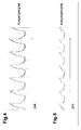
- Fig.4
- ein Ausgangssignal einer kapazitätsgewichteten Sensorschaltung bei nichtbetätigtem kapazitiven Sensor;
- Fig.5
- ein Ausgangssignal einer kapazitätsgewichteten Sensorschaltung bei betätigtem kapazitiven Sensor;
- Fig.6
- ein Diagramm zur Visualisierung eines Übergang des Ausgangssignals bei Berührung des kapazitiven Sensors.
- Fig.1
- an exemplary circuit arrangement for a capacitance-weighted sensor circuit;
- Fig.2
- an alternative circuit arrangement for a capacitance-weighted sensor circuit;
- Figure 3
- an additional circuit example of a capacitance-weighted sensor circuit;
- Figure 4
- an output of a capacitance-weighted sensor circuit when the capacitive sensor is not actuated;
- Figure 5
- an output signal of a capacitance-weighted sensor circuit when the capacitive sensor is actuated;
- Figure 6
- a diagram for visualizing a transition of the output signal when touching the capacitive sensor.
Bei direkter Parallelschaltung eines kapazitiven Sensors zu anderen bekannten Kapazitäten bewirkt ein Berühren des kapazitiven Sensors lediglich eine geringfügige Ladungsverschiebung, die entsprechend aufwändig ausgewertet werden muss.In direct parallel connection of a capacitive sensor to other known capacitances touching the capacitive sensor causes only a slight Charge shift, which must be evaluated correspondingly complex.
Der hier vorgeschlagene Ansatz nutzt einen Verstärker und bindet den kapazitiven Sensor in eine Gegenkopplung des Verstärkers ein. Der Einfluss des kapazitiven Sensors auf das auszuwertende Signal wird entsprechend der Verstärkung des Verstärkers deutlich erhöht. Somit ist eine Zustandsveränderung des kapazitiven Sensors deutlich detektierbar bzw. können zur Detektion einer solchen Zustandsveränderung preiswerte Bauelemente eingesetzt werden. Die Detektion bzw. Auswertung des Signals kann mittels eines Mikrokontrollers, allgemeiner integrierter Schaltungen und/oder diskreter Elektronik erfolgen.The approach proposed here uses an amplifier and integrates the capacitive sensor in a negative feedback of the amplifier. The influence of the capacitive sensor on the signal to be evaluated is significantly increased according to the gain of the amplifier. Thus, a change in state of the capacitive sensor is clearly detectable or can be used to detect such a state change inexpensive components. The detection or evaluation of the signal can be effected by means of a microcontroller, more generally integrated circuits and / or discrete electronics.
Durch die Verstärkung wird die Kapazitätsänderung des Sensors entsprechend der Verstärkung höher gewichtet als bei der bloßen Parallelschaltung des kapazitiven Sensors mit einem Kondensator, so dass die Rückwirkung des kapazitiven Sensors auf den bekannten Kondensator groß wird und zudem über die Verstärkung parametrierbar ist.Due to the gain, the capacitance change of the sensor is weighted higher in accordance with the gain than in the mere parallel connection of the capacitive sensor with a capacitor, so that the reaction of the capacitive sensor is large on the known capacitor and also via the gain can be parameterized.
Der Verstärker kann mindestens eine der folgenden Komponenten umfassen:
- einen Operationsverstärker;
- einen Transistor;
- einen Mosfet.
- an operational amplifier;
- a transistor;
- a mosfet.
Beispielsweise können günstige Schaltungen aus mehreren Transistoren (z.B. umfassend zwei Transistoren) eingesetzt werden, um das Signal des kapazitiven Sensors zu detektieren.For example, favorable circuits of a plurality of transistors (e.g., including two transistors) can be used to detect the signal of the capacitive sensor.
Der kapazitive Sensor kann z.B. realisiert sein, indem ein elektrischer Kontakt der Schaltung an einem Gehäuse nach außen geführt wird und eine Kupfer-Fläche z.B. hinter einem FR-1-Platinen-Material von 1,6mm Dicke angeordnet ist. Die Kupfer-Fläche in dem Gehäuse wird nicht berührt, jedoch ergibt sich eine Kapazitätsänderung durch Berührung des elektrischen Kontakt. Alternativ kann die Kupfer-Fläche auch an der Gehäuse-Innenwand angeordnet sein.
-
Fig.4 zeigt ein Ausgangssignal einer kapazitätsgewichteten Sensorschaltung bei nichtbetätigtem kapazitiven Sensor und -
Fig.5 zeigt ein Ausgangssignal der Schaltung bei Berührung des kapazitiven Sensors.Fig.6 zeigt den Übergang des Ausgangssignals bei Berührung des kapazitiven Sensors. Der Unterschied der beiden Signal bei Berührung und ohne Berührung des Sensors ist aufgrund des hier vorgestellten Ansatzes stark ausgeprägt und kann daher mit geringem elektrischem Aufwand mit hoher Sicherheit detektiert werden.
-
Figure 4 shows an output signal of a capacitance-weighted sensor circuit with non-actuated capacitive sensor and -
Figure 5 shows an output signal of the circuit when touching the capacitive sensor.Figure 6 shows the transition of the output signal when touching the capacitive sensor. The difference between the two signals when touched and without touching the sensor is very pronounced due to the approach presented here and can therefore be detected with high electrical safety with high electrical safety.
Eine Spannungsquelle V2 ist mit ihrem positiven Anschluss mit einem Knoten 102 und mit ihrem negativen Anschluss mit einem Knoten 103 verbunden. Eine Wechselspannungsquelle V1 ist mit ihrem ersten Pol mit dem Knoten 103 und mit ihrem zweiten Pol über einen Widerstand R1 mit der Basis eines npn-Transistors Q1 verbunden. Die Basis des Transistors Q1 ist weiterhin über einen Kondensator C1 mit einem Anschluss 101 verbunden. Der Kollektor des Transistors Q1 ist mit dem Knoten 102 und der Emitter des Transistors Q1 ist über einen Widerstand R2 mit dem Knoten 103 verbunden. Der Emitter des Transistors Q1 ist weiterhin über einen Kondensator C2 mit der Basis eines npn-Transistors Q2 verbunden. Zwischen der Basis des Transistors Q2 und dem Knoten 102 ist ein Widerstand R3 angeordnet. Der Emitter des Transistors Q2 ist mit dem Knoten 103 verbunden und der Kollektor des Transistors Q2 ist einerseits mit dem Anschluss 101 und andererseits über einen Widerstand R4 mit dem Knoten 102 verbunden.A voltage source V2 has its positive terminal connected to a
Bei dem Kondensator C1 handelt es sich um einen kapazitiven Berührungssensor (bzw. bildet dieser Kondensator C1 die Kapazität des Berührungssensors nach). Der Kondensator C1 ist im Gegenkopplungszweig des Verstärkers umfassend die Transistoren Q1 und Q2 angeordnet. Entsprechend der Parametrierung des Verstärkers aus Q1 und Q2 kann die Zustandsveränderung des Sensors ("berührt" bzw. "nicht berührt") mit einer hohen Erkennungsrate robust detektiert werden. Der Aufbau des Verstärkers mit zwei handelsüblichen Transistoren Q1 und Q2 ist äußerst kostengünstig.The capacitor C1 is a capacitive touch sensor (or this capacitor C1 simulates the capacitance of the touch sensor). The capacitor C1 is arranged in the negative feedback branch of the amplifier comprising the transistors Q1 and Q2. According to the parameterization of the amplifier from Q1 and Q2, the state change of the sensor ("touched" or "not touched") can be robustly detected with a high detection rate. The structure of the amplifier with two commercially available transistors Q1 and Q2 is extremely inexpensive.
Der Transistor Q1 arbeitet als Impedanzwandler, der Transistor Q2 wird als ein nichtlinearer Verstärker betrieben, dessen Ausgangsignal eine Ruhelage nahe 0V haben kann. Die Wechselspannungsquelle V1 kann ein Taktsignal bereitstellen, das z.B. von einem Mikrokontroller (nicht dargestellt) zur Verfügung gestellt wird. Die Spannungsquelle V2 kann als eine Batterie ausgeführt sein.The transistor Q1 operates as an impedance converter, the transistor Q2 is operated as a non-linear amplifier, whose output signal may have a rest position near 0V. The AC voltage source V1 may provide a clock signal, e.g. provided by a microcontroller (not shown). The voltage source V2 can be designed as a battery.
Der Wert des Kondensators C1 (Berührungssensor) ist ohne Berührung sehr klein, bei Berührung liegt der Wert des Kondensators C1 im pF-Bereich (im Beispiel von
Der Anschluss 101 liefert ein Ausgangssignal für den Mikrokontroller (nicht dargestellt), der durch geeignete Auswertung erkennt, ob der Berührungssensor berührt wird oder nicht. Entsprechend kann der Mikrokontroller eine vorgegebene Aktion durchführen, z.B. eine Leuchte ansteuern (einschalten, ausschalten, dimmen).The terminal 101 provides an output signal for the microcontroller (not shown), which detects by suitable evaluation whether the touch sensor is touched or not. Accordingly, the microcontroller may perform a predetermined action, e.g. activate a light (switch on, switch off, dimming).
Ein Anwendungsbeispiel für die vorstehend gezeigte Schaltungsanordnung ist die Verwendung in einer Leuchte, z.B. einer portablen Leuchte (Taschenlampe). Über den kapazitiven Sensor (symbolisch dargestellt durch den Kondensator C1 in
Die in
Eine Gleichspannungsquelle V4 (z.B. eine Batterie) ist mit ihrem positiven Pol mit einem Knoten 203 und mit ihrem negativen Pol mit einem Knoten 204 verbunden. Eine Wechselspannungsquelle V3 ist einerseits mit dem Knoten 204 und andererseits über einen Widerstand R5 mit der Basis eines npn-Transistors Q3 verbunden. Die Basis des Transistors Q3 ist über einen Kondensator C3 mit einem Anschluss 202 verbunden, der Anschluss 202 ist über einen Kondensator C4 mit einem Anschluss 201 verbunden, wobei der Anschluss 201 über einen Widerstand R8 mit dem Kollektor eines pnp-Transistors Q4 verbunden ist. Der Emitter des Transistors Q3 ist über einen Widerstand R6 mit dem Knoten 204 verbunden. Der Emitter des Transistors Q3 ist weiterhin über einen Kondensator C5 mit der Basis des Transistors Q4 verbunden. Die Basis des Transistors Q4 ist auch über einen Widerstand R7 mit dem Knoten 203 verbunden, der ferner mit dem Emitter des Transistors Q4 verbunden ist. Der Kollektor des Transistors Q4 ist zusätzlich über einen Widerstand R9 mit dem Knoten 204 verbunden. Schließlich ist der Kollektor des Transistors Q4 über einen Widerstand R10 mit einem Anschluss 205 verbunden, wobei zwischen dem Anschluss 205 und dem Knoten 204 ein Kondensator C6 angeordnet ist.A DC voltage source V4 (eg a battery) is connected with its positive pole to a
Die Kombination aus den Transistoren Q3 und Q4 stellt eine nichtlinear Verstärkerstufe mit Impedanzwandler dar. Die Kondensatoren C3 und C5 dienen einer Brumm-Minimierung. Der Kondensator C3 kann ggf. auch entfallen bzw. durch eine direkte Verbindung ersetzt werden. Der Kondensator C4 entspricht dem kapazitiven Sensor, der einerseits mit einer Kupfer-Fläche (Anschluss 202) innerhalb des Gehäuses und andererseits mit einem aus dem Gehäuse herausgeführten Kontakt (Anschluss 201) verbunden ist. An dem Anschluss 205 liegt das auswertbare Signal an, das optional mittels des RC-Filters aus Widerstand R10 und Kondensator C6 weitgehend auf den Gleichanteil des Ausgangssignals beschränkt wird.The combination of the transistors Q3 and Q4 constitutes a non-linear amplifier stage with impedance converter. The capacitors C3 and C5 serve to minimize hum. If necessary, the capacitor C3 can also be omitted or replaced by a direct connection. The capacitor C4 corresponds to the capacitive sensor, which is connected on the one hand to a copper surface (terminal 202) within the housing and on the other hand to a contact led out of the housing (terminal 201). The evaluable signal is applied to the
Das über den Anschluss 205 bereitgestellte Signal kann unmittelbar von einem Mikrokontroller (nicht dargestellt) ausgewertet werden. Selbstverständlich kann anstelle des Mikrokontrollers auch eine andere digitale oder analoge Auswerteschaltung vorgesehen sein.The signal provided via the
Die in
Eine Gleichspannungsquelle V6 ist mit ihrem positiven Pol mit einem Knoten 303 und mit ihrem negativen Pol mit einem Knoten 304 verbunden. Die Gleichspannungsquelle V6 kann beispielsweise eine (wiederaufladbare) Batterie umfassen. Eine Wechselspannungsquelle V5 ist einerseits mit dem Knoten 304 und andererseits über einen Widerstand R11 mit der Basis eines pnp-Transistors Q5 verbunden. Die Basis des Transistors Q5 ist weiterhin über einen Kondensator C7 mit einem Anschluss 302 verbunden. Zusätzlich ist die Basis des Transistors Q5 über einen Widerstand R12 mit dem Emitter des Transistors Q5 verbunden. Der Kollektor des Transistors Q5 ist mit dem Knoten 304 verbunden. Der Emitter des Transistors Q5 ist ferner über einen Widerstand R13 mit dem Knoten 303 verbunden. Auch ist der Emitter des Transistors Q5 über einen Kondensator C9 mit der Basis eines pnp-Transistors Q6 verbunden. Die Basis des Transistors Q6 ist über einen Widerstand R14 mit dem Knoten 303 verbunden, der wiederum mit dem Emitter des Transistors Q6 verbunden ist. Der Anschluss 302 ist über einen Kondensator C8 mit einem Anschluss 301 verbunden, wobei der Anschluss 301 über einen Widerstand R15 mit dem Kollektor des Transistors Q6 verbunden ist. Der Kollektor des Transistors Q6 ist ferner über einen Widerstand R16 mit dem Knoten 304 verbunden. Auch ist der Kollektor des Transistors Q6 über einen Widerstand R17 mit einem Anschluss 305 verbunden. Zwischen dem Anschluss 305 und dem Knoten 304 ist eine Parallelschaltung aus einem Kondensator C10 und einem Widerstand R18 angeordnet.A DC voltage source V6 has its positive pole connected to a
Die Anordnung gemäß
Die Anschlüsse 301, 302 und 305 entsprechen funktional den Anschlüssen 201, 202 und 205 gemäß
Die in
Claims (15)
Applications Claiming Priority (1)
| Application Number | Priority Date | Filing Date | Title |
|---|---|---|---|
| DE200910021719 DE102009021719A1 (en) | 2009-05-18 | 2009-05-18 | sensor circuit |
Publications (1)
| Publication Number | Publication Date |
|---|---|
| EP2254247A1 true EP2254247A1 (en) | 2010-11-24 |
Family
ID=42711892
Family Applications (1)
| Application Number | Title | Priority Date | Filing Date |
|---|---|---|---|
| EP10160739A Withdrawn EP2254247A1 (en) | 2009-05-18 | 2010-04-22 | Sensor circuit |
Country Status (3)
| Country | Link |
|---|---|
| EP (1) | EP2254247A1 (en) |
| CN (1) | CN101895287A (en) |
| DE (1) | DE102009021719A1 (en) |
Families Citing this family (2)
| Publication number | Priority date | Publication date | Assignee | Title |
|---|---|---|---|---|
| CN105183258A (en) * | 2015-09-23 | 2015-12-23 | 深圳信炜科技有限公司 | Sensing unit of capacitive sensor and sensing unit group |
| CN105224155A (en) * | 2015-09-23 | 2016-01-06 | 深圳信炜科技有限公司 | Capacitance type sensor, sensing device, sensing system and electronic equipment |
Citations (10)
| Publication number | Priority date | Publication date | Assignee | Title |
|---|---|---|---|---|
| US2848659A (en) * | 1955-03-28 | 1958-08-19 | Gen Electric | Electronic control switch |
| DE2203039A1 (en) * | 1972-01-22 | 1973-07-26 | Robert Buck | ELECTRONIC, CONTACTLESS SWITCHING DEVICE |
| GB2005422A (en) * | 1977-10-05 | 1979-04-19 | Buck R | Proximity switches |
| DE3600978A1 (en) * | 1986-01-15 | 1987-07-16 | Siemens Ag | Amplifier circuit for a high-impedance sensor |
| JPH0229121A (en) * | 1988-07-19 | 1990-01-31 | Hisao Funahara | Touch switch |
| JPH0296425A (en) * | 1988-09-30 | 1990-04-09 | Hisao Funahara | Oscillating circuit for touch switch |
| EP0448988A1 (en) * | 1990-03-27 | 1991-10-02 | FIFE GmbH | Apparatus for contactless detection of the position of a moving web |
| JPH0563538A (en) * | 1991-09-04 | 1993-03-12 | Kyosan Electric Mfg Co Ltd | Optical interrupter circuit |
| US7023221B1 (en) * | 2005-05-09 | 2006-04-04 | Holylite Microectronics Corporation | Structure of object proximity and position detector |
| EP1791260A1 (en) * | 2005-11-24 | 2007-05-30 | Holylite Microelectronics Corporation | Object proximity or position detector |
Family Cites Families (9)
| Publication number | Priority date | Publication date | Assignee | Title |
|---|---|---|---|---|
| DE3042007A1 (en) * | 1980-11-07 | 1982-06-24 | Miele & Cie GmbH & Co, 4830 Gütersloh | Electronic touch control switch - uses operational amplifier with resistive feed back comparing sensor electrode signal with reference signal |
| JPS6029969B2 (en) * | 1982-06-18 | 1985-07-13 | 富士通株式会社 | touch detection device |
| EP0711405B1 (en) * | 1993-07-30 | 1997-05-02 | Andrej Zatler | Self-adjusting capacitive level switch for a non-contact or contact sensing of media or objects |
| JP3233791B2 (en) * | 1994-08-25 | 2001-11-26 | 株式会社山武 | Differential capacitance inverting integrator and capacitance change amount detecting device using the same |
| DE19823544C2 (en) * | 1998-05-27 | 2003-06-05 | Univ Ilmenau Tech | Circuit arrangement for measuring small changes in electrical quantities |
| DE10131243C1 (en) * | 2001-06-28 | 2002-11-07 | Luer Luetkens | Capacitive proximity switch e.g. for production line robot, uses difference signal between 2 screened sensor electrodes |
| DE10156580B4 (en) * | 2001-11-20 | 2005-08-11 | Sie Sensorik Industrie-Elektronik Gmbh | Oscillator circuits for detecting small capacitances or capacitance differences for use in capacitive sensors |
| DE102005041113A1 (en) * | 2005-08-30 | 2007-03-01 | BSH Bosch und Siemens Hausgeräte GmbH | Capacitive proximity switch for e.g. washing machine, has semiconductor switch comprising signal input with clock signal and signal output, where output has output signal, which has signals portions that are proportional to capacitance |
| DE102007033886B4 (en) * | 2007-07-20 | 2009-04-30 | Siemens Ag | Output unit for outputting different signals; electrical component for controlling an electrical device and method for outputting different signals by an output unit |
-
2009
- 2009-05-18 DE DE200910021719 patent/DE102009021719A1/en not_active Ceased
-
2010
- 2010-04-22 EP EP10160739A patent/EP2254247A1/en not_active Withdrawn
- 2010-05-18 CN CN2010101823154A patent/CN101895287A/en active Pending
Patent Citations (10)
| Publication number | Priority date | Publication date | Assignee | Title |
|---|---|---|---|---|
| US2848659A (en) * | 1955-03-28 | 1958-08-19 | Gen Electric | Electronic control switch |
| DE2203039A1 (en) * | 1972-01-22 | 1973-07-26 | Robert Buck | ELECTRONIC, CONTACTLESS SWITCHING DEVICE |
| GB2005422A (en) * | 1977-10-05 | 1979-04-19 | Buck R | Proximity switches |
| DE3600978A1 (en) * | 1986-01-15 | 1987-07-16 | Siemens Ag | Amplifier circuit for a high-impedance sensor |
| JPH0229121A (en) * | 1988-07-19 | 1990-01-31 | Hisao Funahara | Touch switch |
| JPH0296425A (en) * | 1988-09-30 | 1990-04-09 | Hisao Funahara | Oscillating circuit for touch switch |
| EP0448988A1 (en) * | 1990-03-27 | 1991-10-02 | FIFE GmbH | Apparatus for contactless detection of the position of a moving web |
| JPH0563538A (en) * | 1991-09-04 | 1993-03-12 | Kyosan Electric Mfg Co Ltd | Optical interrupter circuit |
| US7023221B1 (en) * | 2005-05-09 | 2006-04-04 | Holylite Microectronics Corporation | Structure of object proximity and position detector |
| EP1791260A1 (en) * | 2005-11-24 | 2007-05-30 | Holylite Microelectronics Corporation | Object proximity or position detector |
Also Published As
| Publication number | Publication date |
|---|---|
| CN101895287A (en) | 2010-11-24 |
| DE102009021719A1 (en) | 2010-11-25 |
Similar Documents
| Publication | Publication Date | Title |
|---|---|---|
| EP2359476B1 (en) | Capacitive sensor system | |
| DE102006029120B4 (en) | Circuit arrangement for detecting the capacitance or a capacitance change of a capacitive circuit or component | |
| EP0859468A1 (en) | Circuitry for a sensor element | |
| EP0496246A1 (en) | Circuit for operating a discharge lamp | |
| EP1925082A1 (en) | Capacitive proximity switch and domestic appliance comprising the same | |
| EP1925081A1 (en) | Capacitive proximity switch and household appliance equipped therewith | |
| DE102008036155B4 (en) | control button layout | |
| EP2254247A1 (en) | Sensor circuit | |
| EP0131146A1 (en) | Electronic switching device, preferably operating without making contact | |
| DE10121008B4 (en) | Capacitive keyboard with evaluation circuit | |
| EP0298331A2 (en) | Electronic switching device operating without contact | |
| EP3690967A1 (en) | Control circuit and method for controlling a piezoelectric transformer | |
| DE102015107498A1 (en) | COMPREHENSIVE PROXIMITY SWITCH ASSEMBLY AND ACTIVATION METHOD | |
| EP1952521B1 (en) | Double universal dimmer | |
| DE102004036958A1 (en) | Control of circuit breakers | |
| WO2008092931A1 (en) | Circuit arrangement, and method for the operation of a circuit arrangement | |
| DE102015109548A1 (en) | Proximity switch arrangement with mating surface and recess | |
| DE4027386C1 (en) | ||
| EP2507913B1 (en) | Household appliance having a control apparatus and method for operating a household appliance | |
| DE102018211024A1 (en) | Method and sensor device for detecting an approach to two capacitive sensor electrodes | |
| EP2230766A1 (en) | Switch assembly for determining a capacity of a capacitive sensor element | |
| EP2230765B1 (en) | Sensor device, method for detecting an operator control action and operating device | |
| EP2341623B1 (en) | Touch-sensitive sensor | |
| CN104579170B (en) | relaxation oscillator | |
| DE102011105076B4 (en) | System and method for evaluating a module |
Legal Events
| Date | Code | Title | Description |
|---|---|---|---|
| PUAI | Public reference made under article 153(3) epc to a published international application that has entered the european phase |
Free format text: ORIGINAL CODE: 0009012 |
|
| AK | Designated contracting states |
Kind code of ref document: A1 Designated state(s): AT BE BG CH CY CZ DE DK EE ES FI FR GB GR HR HU IE IS IT LI LT LU LV MC MK MT NL NO PL PT RO SE SI SK SM TR |
|
| AX | Request for extension of the european patent |
Extension state: AL BA ME RS |
|
| STAA | Information on the status of an ep patent application or granted ep patent |
Free format text: STATUS: THE APPLICATION IS DEEMED TO BE WITHDRAWN |
|
| 18D | Application deemed to be withdrawn |
Effective date: 20110427 |