EP2359476B1 - Capacitive sensor system - Google Patents
Capacitive sensor system Download PDFInfo
- Publication number
- EP2359476B1 EP2359476B1 EP09799244.0A EP09799244A EP2359476B1 EP 2359476 B1 EP2359476 B1 EP 2359476B1 EP 09799244 A EP09799244 A EP 09799244A EP 2359476 B1 EP2359476 B1 EP 2359476B1
- Authority
- EP
- European Patent Office
- Prior art keywords
- circuit arrangement
- arrangement according
- electrode
- circuit
- gate
- Prior art date
- Legal status (The legal status is an assumption and is not a legal conclusion. Google has not performed a legal analysis and makes no representation as to the accuracy of the status listed.)
- Active
Links
Images


Classifications
-
- H—ELECTRICITY
- H03—ELECTRONIC CIRCUITRY
- H03K—PULSE TECHNIQUE
- H03K17/00—Electronic switching or gating, i.e. not by contact-making and –breaking
- H03K17/94—Electronic switching or gating, i.e. not by contact-making and –breaking characterised by the way in which the control signals are generated
- H03K17/945—Proximity switches
- H03K17/955—Proximity switches using a capacitive detector
-
- G—PHYSICS
- G06—COMPUTING; CALCULATING OR COUNTING
- G06F—ELECTRIC DIGITAL DATA PROCESSING
- G06F3/00—Input arrangements for transferring data to be processed into a form capable of being handled by the computer; Output arrangements for transferring data from processing unit to output unit, e.g. interface arrangements
- G06F3/01—Input arrangements or combined input and output arrangements for interaction between user and computer
- G06F3/011—Arrangements for interaction with the human body, e.g. for user immersion in virtual reality
-
- G—PHYSICS
- G06—COMPUTING; CALCULATING OR COUNTING
- G06F—ELECTRIC DIGITAL DATA PROCESSING
- G06F3/00—Input arrangements for transferring data to be processed into a form capable of being handled by the computer; Output arrangements for transferring data from processing unit to output unit, e.g. interface arrangements
- G06F3/01—Input arrangements or combined input and output arrangements for interaction between user and computer
- G06F3/017—Gesture based interaction, e.g. based on a set of recognized hand gestures
-
- G—PHYSICS
- G06—COMPUTING; CALCULATING OR COUNTING
- G06F—ELECTRIC DIGITAL DATA PROCESSING
- G06F3/00—Input arrangements for transferring data to be processed into a form capable of being handled by the computer; Output arrangements for transferring data from processing unit to output unit, e.g. interface arrangements
- G06F3/01—Input arrangements or combined input and output arrangements for interaction between user and computer
- G06F3/03—Arrangements for converting the position or the displacement of a member into a coded form
- G06F3/041—Digitisers, e.g. for touch screens or touch pads, characterised by the transducing means
- G06F3/044—Digitisers, e.g. for touch screens or touch pads, characterised by the transducing means by capacitive means
-
- H—ELECTRICITY
- H03—ELECTRONIC CIRCUITRY
- H03K—PULSE TECHNIQUE
- H03K2217/00—Indexing scheme related to electronic switching or gating, i.e. not by contact-making or -breaking covered by H03K17/00
- H03K2217/94—Indexing scheme related to electronic switching or gating, i.e. not by contact-making or -breaking covered by H03K17/00 characterised by the way in which the control signal is generated
- H03K2217/96—Touch switches
- H03K2217/9607—Capacitive touch switches
- H03K2217/960705—Safety of capacitive touch and proximity switches, e.g. increasing reliability, fail-safe
-
- H—ELECTRICITY
- H03—ELECTRONIC CIRCUITRY
- H03K—PULSE TECHNIQUE
- H03K2217/00—Indexing scheme related to electronic switching or gating, i.e. not by contact-making or -breaking covered by H03K17/00
- H03K2217/94—Indexing scheme related to electronic switching or gating, i.e. not by contact-making or -breaking covered by H03K17/00 characterised by the way in which the control signal is generated
- H03K2217/96—Touch switches
- H03K2217/9607—Capacitive touch switches
- H03K2217/96071—Capacitive touch switches characterised by the detection principle
- H03K2217/960715—Rc-timing; e.g. measurement of variation of charge time or discharge time of the sensor
-
- H—ELECTRICITY
- H03—ELECTRONIC CIRCUITRY
- H03K—PULSE TECHNIQUE
- H03K2217/00—Indexing scheme related to electronic switching or gating, i.e. not by contact-making or -breaking covered by H03K17/00
- H03K2217/94—Indexing scheme related to electronic switching or gating, i.e. not by contact-making or -breaking covered by H03K17/00 characterised by the way in which the control signal is generated
- H03K2217/96—Touch switches
- H03K2217/9607—Capacitive touch switches
- H03K2217/96071—Capacitive touch switches characterised by the detection principle
- H03K2217/96072—Phase comparison, i.e. where a phase comparator receives at one input the signal directly from the oscillator, at a second input the same signal but delayed, with a delay depending on a sensing capacitance
-
- H—ELECTRICITY
- H03—ELECTRONIC CIRCUITRY
- H03K—PULSE TECHNIQUE
- H03K2217/00—Indexing scheme related to electronic switching or gating, i.e. not by contact-making or -breaking covered by H03K17/00
- H03K2217/94—Indexing scheme related to electronic switching or gating, i.e. not by contact-making or -breaking covered by H03K17/00 characterised by the way in which the control signal is generated
- H03K2217/96—Touch switches
- H03K2217/9607—Capacitive touch switches
- H03K2217/960755—Constructional details of capacitive touch and proximity switches
- H03K2217/960765—Details of shielding arrangements
Definitions
- the invention relates to a capacitive sensor system, in particular for detecting object approaches and in particular also for gesture recognition.
- the invention relates to a sensor system in which the approach or movement, typically of a hand or a finger, is detected on the basis of electrical near fields and from which information is derived which can be used to control switching operations or to recognize a spatial gesture.
- the evaluation of the change in capacitance of an RC low-pass element is known for a capacitive sensor system.
- a sinusoidal voltage or a square wave signal is used as the excitation signal.
- the amplitude or phase or the time shift compared to a reference signal is evaluated as a signal indicator for the change.
- the relative change ⁇ C / C of the change in capacitance compared to a basic capacitance C is important, since this means that Sensor sensitivity or the maximum detection range of the sensor is determined. The lowest possible basic capacity should therefore be aimed for maximum sensitivity.
- a capacitive sensor arrangement is from the document WO 98/07051 known.
- the object of the present invention is to provide a capacitively operating sensor system which can be implemented with low component expenditure and thus low costs and space requirements and which is also characterized by low power consumption in order to be able to work with batteries with a low charge capacity or a long operating life.
- FIG. 1a A circuit arrangement according to the invention is shown. This comprises a capacitive proximity sensor constructed according to the invention. This circuit arrangement can be expanded by multiple designs to form a sensor system for gesture recognition.
- the parasitic capacitances are formed on the one hand by the field coupling between a signal electrode designated E s and a ground electrode Eg of the circuit arrangement (C1) and on the other hand by coupling capacitances C2 and C3 from a hand approaching these electrodes.
- the capacitances C4 and C5 are coupling capacitances of the hand or the circuit ground to earth.
- the course for reaching a certain threshold value u S1 is t1.
- the discharge then takes place after half a period T of the square-wave signal corresponding to u E and again reaches a threshold value u S2 after a time t2.
- Eq. 4 shows that the closer the threshold u S1 is to u 0 and the smaller u S2 in relation to u 0 , the greater the ⁇ t. This means that a suitable hysteresis of a threshold decision maker is favorable when selecting the threshold values.
- a further contribution to C1 is made by the coupling capacitance between the signal electrode E S and the electrode E G connected to ground.
- a so-called shield electrode can be inserted between them, which is connected to the output of the source follower and is therefore at almost the same potential as the gate, as a result of which the coupling E S and E G is considerably reduced.
- the source output of the FET can also be used to drive the shield of a coaxial cable when the signal electrode ES is located further away and thereby reduce the cable capacity, which would also make a contribution to C1.
- An XOR gate is used to evaluate the time shift of the charging and discharging process, the inputs of which are switched via integrated Schmitt triggers, which means that no additional comparator is required for the switching thresholds uS1 and uS2 and additional components can be saved.
- the coupling to the ground electrode E G does not necessarily have to take place by means of a separate electrode, but, depending on the application, can also be provided by a different type of coupling, for example via the batteries.
- Fig. 1a Due to the arrangement of Fig. 1a There are diverse applications and design options, in particular through electrode shapes and electrode configurations, examples of which are given below. With Fig. 1a Given arrangement according to the invention is characterized not only by an extremely low cost of components and thus costs and small space requirements, but also by an extremely low power consumption in the sensor, which is essentially given by the current flowing through the source resistance of the FET. With values of this resistance in the range of a few kOhm, currents far below 1mA can be realized with this.
- a special feature of this arrangement is that the sensor can be operated in pulsed mode without any particular transient problems. In applications with battery operation, this is often a mandatory measure to ensure battery discharge in the range of only a few ⁇ A and thus to achieve a correspondingly long operating time.
- pulse operation there is no longer a DC voltage at the output of the low pass, but an in Fig. 3 shown charging and discharging pulse.
- ⁇ u Pulse amplitude by a value ⁇ u, which corresponds to that of continuous operation according to Eq. 5 corresponds.
- a cordless computer mouse is switched to the active state by the sensor system according to the invention when the hand approaches, in order to limit the battery current to the lowest possible value.
- the signal electrode is attached to part of the inside of the upper shell of the housing and can also be surrounded by a strip-shaped ground electrode.
- the exact design of the electrodes depends on the shape of the housing, and depending on the design of the mouse electronics and the associated battery supply, separate ground electronics may also be dispensed with if there is sufficient ground coupling of the hand in another way, for example via the batteries.
- pulse operation in a ratio of, for example, 1: 1000, the current consumption from the battery can be reduced to 1..2 ⁇ A by the sensors.
- the proximity sensor is the recognition of gestures using a 4-electrode system, the principle of which is shown in Figure 5 is illustrated in detail.
- the electrode system including the associated sensor electronics, should remain concentrated in the most compact possible form in a small space in order to be able to integrate it in a space-saving manner in existing facilities of various types. This also results in the further advantages of low-current operation with regard to battery applications and cost-effective implementation which have already been explained above.
- the task is to derive the x / y coordinates of a gesture movement with respect to the plane spanned by the electrodes from the information provided by the sensors.
- the x / y coordinates can be calculated in a simple manner independently of z.
- the distances r 1 to r 4 must be determined from the signals which are present at the output of the 4 sensors S1 to S4. Only the signal differences that arise when approaching the basic state are considered. These difference signals are denoted by e 1 to e 4 and are derived from the capacitance changes described above at the respective gates of the field effect transistors.
- the decisive factor here is the coupling capacity of the finger to the electrodes, which decreases with increasing distance from the electrode. Since the delivered amplitude of the signal difference according to the explanations from above is proportional to the change in capacitance, these values decrease with increasing distance.
- the constants e 0 , r 0 and a are dependent on the respective electrode shape and arrangement of the electrodes.
- FIG. 6 Various electrode arrangements are shown, which are either directly coupled to the electronics with short connections and thus form a compact unit that is only a few cm 2 in size, which can be easily integrated into other systems or can also be further away from the electronics by means of coaxial cables, for which purpose then preferably the cable shield is connected to the shielding output of the sensor (source connection of the FET) in order to keep the basic capacitance C1 at the gate connection low.
- a special measure in the circuit according to the invention lies in the particularly simple and thus energy and cost-saving implementation of the proximity sensor with a single FET stage and a downstream EXOR gate without the need for an additional comparator.
- the FET stage as far as it is switched as a source follower, provides an extremely low input capacitance and thus allows a high series resistance, which is decisive for the sensitivity, which is up to a factor of 50 higher than that of conventional sensors.
- the stage in this configuration also offers a shielding function, which can be used to keep the basic input capacitance low in critical installation situations and thus prevent a relevant loss of sensitivity.
- the concept according to the invention is characterized by a particularly low power consumption and is particularly suitable for battery applications.
- the costs, which are mainly determined by the number of active components of a circuit arrangement, and the space requirement are significantly less than in the case of conventional concepts.
- the circuit concept according to the invention is particularly advantageously suitable for systems with a simultaneous operation of several sensors, e.g. for gesture applications.
Landscapes
- Engineering & Computer Science (AREA)
- General Engineering & Computer Science (AREA)
- Theoretical Computer Science (AREA)
- Human Computer Interaction (AREA)
- Physics & Mathematics (AREA)
- General Physics & Mathematics (AREA)
- Electronic Switches (AREA)
- Measurement Of Length, Angles, Or The Like Using Electric Or Magnetic Means (AREA)
- Geophysics And Detection Of Objects (AREA)
Description
Die Erfindung richtet sich auf ein kapazitives Sensorsystem insbesondere zur Erfassung von Objektannäherungen sowie insbesondere auch zur Gestenerkennung. Die Erfindung betrifft dabei ein Sensorsystem, bei welchem auf der Basis elektrischer Nahfelder die Annäherung bzw. Bewegung typischerweise einer Hand oder eines Fingers detektiert wird und hieraus Informationen abgeleitet werden, die zur Steuerung von Schaltvorgängen oder zum Erkennen einer räumlichen Geste herangezogen werden können.The invention relates to a capacitive sensor system, in particular for detecting object approaches and in particular also for gesture recognition. The invention relates to a sensor system in which the approach or movement, typically of a hand or a finger, is detected on the basis of electrical near fields and from which information is derived which can be used to control switching operations or to recognize a spatial gesture.
Insbesondere zur Gestenerkennung gibt es optische Verfahren im sichtbaren oder InfrarotBereich. Ferner sind kapazitiv wirkende Systeme bekannt, die über die Übertragung oder Störung eines elektrischen Feldes die erforderlichen Informationen gewinnen. Der schaltungstechnische Aufwand und die mit der Realisierung derartiger System verbundenen Kosten sind bislang hoch. Ein weiterer Problempunkt bei den herkömmlichen Systemen besteht darin, dass bei Anwendungen, die einen Batteriebetrieb erfordern, der Strombedarf solcher Sensoren entscheidend für die praktische Einsetzbarkeit ist. Weiterhin sind bei manchen Anwendungen die Bauteilkosten und der Raumbedarf von Bedeutung, die bzw. der bei Massen-Anwendungen, z.B. im Bereich der Spielzeugindustrie für die Einsatzmöglichkeit ausschlaggebend sein können.In particular for gesture recognition, there are optical methods in the visible or infrared range. Furthermore, capacitively acting systems are known which obtain the necessary information about the transmission or disturbance of an electrical field. The circuitry outlay and the costs associated with the implementation of such systems have so far been high. Another problem with the conventional systems is that in applications that require battery operation, the power consumption of such sensors is critical for practical use. Furthermore, in some applications the component costs and space requirements are of importance, which in mass applications, e.g. can be decisive for the possible application in the toy industry.
Für eine kapazitives Sensorsystem ist die Auswertung der Kapazitätsänderung eines RC-Tiefpassgliedes bekannt. Als Anregungssignal wird hierbei eine sinusförmige Spannung oder auch ein Rechtecksignal verwendet. Als Signalindikator für die Änderung wird die Amplitude oder die Phase bzw. die Zeitverschiebung gegenüber einem Referenzsignal ausgewertet. Bei beiden Ansätzen (Amplitude oder Phase) kommt es auf die relative Änderung ΔC/C der Kapazitätsänderung gegenüber einer Grundkapazität C an, da hierdurch die Sensorempfindlichkeit bzw. die maximale Detektionsreichweite des Sensors bestimmt wird. Eine möglichst geringe Grundkapazität ist daher für eine maximale Empfindlichkeit anzustreben.The evaluation of the change in capacitance of an RC low-pass element is known for a capacitive sensor system. A sinusoidal voltage or a square wave signal is used as the excitation signal. The amplitude or phase or the time shift compared to a reference signal is evaluated as a signal indicator for the change. In both approaches (amplitude or phase), the relative change ΔC / C of the change in capacitance compared to a basic capacitance C is important, since this means that Sensor sensitivity or the maximum detection range of the sensor is determined. The lowest possible basic capacity should therefore be aimed for maximum sensitivity.
Eine kapazitive Sensoranordnung ist aus dem Dokument
Aufgabe der vorliegenden Erfindung ist es, ein kapazitiv arbeitendes Sensorsystem bereitzustellen, das mit geringem Bauteileaufwand und damit geringen Kosten und Platzbedarf realisierbar ist und sich zudem auch durch einen niedrigen Stromverbrauch auszeichnet, um mit Batterien geringer Ladungskapazität bzw. hoher Betriebsdauer arbeiten zu können.The object of the present invention is to provide a capacitively operating sensor system which can be implemented with low component expenditure and thus low costs and space requirements and which is also characterized by low power consumption in order to be able to work with batteries with a low charge capacity or a long operating life.
Diese Aufgabe wird erfindungsgemäß durch eine Schaltungsanordnung mit den in Patentanspruch 1 angegebenen Merkmalen gelöst.This object is achieved by a circuit arrangement with the features specified in
Durch mehrere derartige Systeme ist es möglich eine 2- oder 3-dimensionale Positionserfassung zu bewerkstelligen. Es ist auch möglich, mehrere Sensorelektroden vorzusehen, und diese über eine Multiplexereinrichtung sukzessive an die Schaltung anzukoppeln. Diese Multiplexerschaltung kann durch den Mikrokontroller getriggert werden. Vorteilhafte Ausgestaltungen der erfindungsgemäßen Schaltungsanordnung sind Gegenstand der Unteransprüche.Several systems of this type make it possible to carry out a 2- or 3-dimensional position detection. It is also possible to provide a plurality of sensor electrodes and to couple them successively to the circuit via a multiplexer device. This multiplexer circuit can be triggered by the microcontroller. Advantageous embodiments of the circuit arrangement according to the invention are the subject of the dependent claims.
Weitere Einzelheiten und Merkmale der Erfindung ergeben sich aus der nachfolgenden Beschreibung in Verbindung mit der Zeichnung. Es zeigt:
- Figur 1a
- eine Schaltungsskizze zur Veranschaulichung des Aufbaus einer erfindungsgemäßen Schaltungsanordnung;
- Figur 1b
- ein Ersatzschaltbild zur weiteren Veranschaulichung der im Rahmen einer Objektannäherung hinsichtlich ihrer Kapazität veränderten Kondensatoreinrichtungen,
-
Figur 2 - ein Diagramm zur Veranschaulichung des Spannungsaufbaus;
- Figur 3
- ein weiteres Diagramm zur Veranschaulichung des Spannungsaufbaus;
- Figur 4
- eine Skizze zur Veranschaulichung des Einsatzes einer erfindungsgemäßen Schaltung bei einer Computermaus;
- Figur 5
- eine Skizze zur Veranschaulichung des Einsatzes eines mehrere Detektionselektroden umfassenden Gestenerfassungssystems;
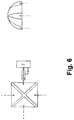
- Figur 6
- zwei Skizzen zur Veranschaulichung der Realisierung erfindungsgemäßer Gestenerfassungssystem unter Verwendung relativ nahe nebeneinanderliegender Detektionselektroden.
- Figure 1a
- a circuit diagram to illustrate the structure of a circuit arrangement according to the invention;
- Figure 1b
- 2 shows an equivalent circuit diagram to further illustrate the capacitance of the capacitor devices which have been changed in the context of an object approach,
- Figure 2
- a diagram illustrating the voltage build-up;
- Figure 3
- another diagram to illustrate the voltage build-up;
- Figure 4
- a sketch to illustrate the use of a circuit according to the invention in a computer mouse;
- Figure 5
- a sketch to illustrate the use of a gesture detection system comprising several detection electrodes;
- Figure 6
- two sketches to illustrate the implementation of the gesture detection system according to the invention using relatively closely adjacent detection electrodes.
In
Zunächst wird die Funktionsweise dieser in
Die parasitären Kapazitäten werden einmal gebildet durch die Feldkopplung zwischen einer mit Es bezeichneten Signalelektrode und einer Groundelektrode Eg der Schaltungsanordnung (C1) und zum anderen durch Kopplungskapazitäten C2 und C3 von einer sich an diese Elektroden nähernden Hand.The parasitic capacitances are formed on the one hand by the field coupling between a signal electrode designated E s and a ground electrode Eg of the circuit arrangement (C1) and on the other hand by coupling capacitances C2 and C3 from a hand approaching these electrodes.
Die Kapazitäten C4 und C5 sind Kopplungskapazitäten der Hand bzw. des Schaltungsgrounds gegen Erde. Zunächst wird die Auf- und Entladung im Grundzustand ohne Annäherung (C2 = C3 = C4 = 0) betrachtet, wodurch nur C1 wirksam ist. Der Verlauf zum Erreichen eines bestimmten Schwellwertes uS1 sei t1. Die Entladung erfolgt dann nach einer halben Periodendauer T des Rechtecksignales entsprechend uE und erreicht nach einer Zeit t2 wieder einen Schwellwert uS2.The capacitances C4 and C5 are coupling capacitances of the hand or the circuit ground to earth. First, the charging and discharging in the basic state is considered without approximation (C2 = C3 = C4 = 0), which means that only C1 is effective. The course for reaching a certain threshold value u S1 is t1. The discharge then takes place after half a period T of the square-wave signal corresponding to u E and again reaches a threshold value u S2 after a time t2.
Daher gilt: ![]()
![]()
Hieraus ergibt sich dann für die Schaltzeiten ![]()
![]()
Bei einer Kapazitätsänderung um ΔC auf C1+ΔC beträgt dann die Zeitverschiebung bei den Schwellwerten ![]()
![]()
Die gesamte Zeitverschiebung ist dann ![]()
![]()
Gl.4 zeigt, dass Δt umso größer wird, je näher die Schwelle uS1 an u0 liegt und je kleiner uS2 im Verhältnis zu u0 wird. Dies bedeutet, dass bei der Wahl der Schwellwerte eine geeignete Hysterese eines Schwellwertentscheiders günstig ist.Eq. 4 shows that the closer the threshold u S1 is to u 0 and the smaller u S2 in relation to u 0 , the greater the Δt. This means that a suitable hysteresis of a threshold decision maker is favorable when selecting the threshold values.
Im Falle uS1=uS2 ist es vorteilhaft, entweder die Schwelle möglichst nahe an u0 oder 0 zu legen, da dann einer der beiden Terme in Gl.4 möglichst groß wird. Ferner ist die Zeitverschiebung und damit die Empfindlichkeit des Sensors umso höher, je größer der Ladewiderstand R und je größer die Kapazitätsänderung ΔC wird. Der Ladewiderstand darf dabei maximal so groß werden, dass es jeweils während einer Halbperiode T/2 des Rechtecksignales noch zu einer nahezu vollständigen Auf- und Entladung am Gate-Eingang eines Feldeffekttransistors kommt. Da R möglichst groß werden soll, hängt diese Forderung entscheidend von der zwischen Gate und Ground wirksamen Kapazität C1 ab (siehe
Einen weiteren Beitrag zu C1 liefert die Kopplungskapazität zwischen der Signalelektrode ES und der mit Ground verbundenen Elektrode EG. Um diese zu minimieren kann dazwischen eine sog. Shield-Elektrode eingefügt werden, die am Ausgang des Sourcefolgers angeschlossen wird und daher auf nahezu gleichem Potential wie das Gate liegt, wodurch die Kopplung ES und EG erheblich vermindert wird. Dies ist ein weiterer vorteilhafter Aspekt der FET-Stufe. Der Source Ausgang des FET kann auch dazu verwendet werden, bei weiter weg gelegenem Anschluss der Signalelektrode ES den Schirm eines Koaxialkabels zu treiben und dadurch die Kabelkapazität zu verringern, die ebenfalls einen Beitrag zu C1 liefern würde.A further contribution to C1 is made by the coupling capacitance between the signal electrode E S and the electrode E G connected to ground. In order to minimize this, a so-called shield electrode can be inserted between them, which is connected to the output of the source follower and is therefore at almost the same potential as the gate, as a result of which the coupling E S and E G is considerably reduced. This is another advantageous aspect of the FET stage. The source output of the FET can also be used to drive the shield of a coaxial cable when the signal electrode ES is located further away and thereby reduce the cable capacity, which would also make a contribution to C1.
Die Ausführungen zeigen auf, dass die Verwendung eines FET's in Sourcefolger-Schaltung als Eingangsstufe erhebliche Vorteile mit sich bringt und zudem den Bauteileaufwand auf ein Minimum reduziert, wodurch sowohl Strombedarf als auch die Kosten sehr gering bleiben.The explanations show that the use of an FET in a source follower circuit as an input stage has considerable advantages and also reduces the component expenditure to a minimum, as a result of which both power consumption and costs remain very low.
Zur Auswertung der bei Annäherung erfolgten Zeitverschiebung des Auf- und Entladevorganges wird ein XOR-Gatter verwendet, dessen Eingänge über integrierte Schmitt-Trigger geschaltet werden , wodurch kein zusätzlicher Comparator für die Schaltschwellen uS1 und uS2 notwendig ist und damit weitere Bauteile eingespart werden können. Die Zeitverschiebung wird repräsentiert durch eine Gleichspannung, die mittels eines am XOR-Ausgang angeschlossen Tiefpassfilters gewonnen wird. Bei einer Versorgungsspannung uB ist diese dann analog zu Gl.4 ![]()
![]()
Setzt man hierin 1/T = f , so erkennt man, dass die am Tiefpass-Ausgang gebildete Gleichspannung proportional zur Frequenz f des vom µC gelieferten Rechtecksignales ist. Da infolge unvermeidlicher Toleranzen, z.B. bei den Schwellwerten, diese Spannung in einem Produktionsprozess unterschiedlich sein kann, besteht eine Möglichkeit zum Toleranzausgleich darin , die Signalfrequenz über den µC so zu verändern, dass sich im Fall keiner Annäherung stets eine konstante Ausgangsspannung ergibt.If 1 / T = f is set here, it can be seen that the DC voltage formed at the low-pass output is proportional to the frequency f of the square-wave signal supplied by the µC. Because due to inevitable tolerances, for example with the threshold values, this voltage in one Production process can be different, there is a way to compensate for tolerance is to change the signal frequency via the µC so that there is always a constant output voltage in the event of no approach.
Entscheidend für die Empfindlichkeit einer Näherungserkennung ist die kapazitive Änderung ΔC am Gate-Eingang, die nach Gl. 4 zu einer entsprechenden Zeitverschiebung □t und damit am Tiefpassausgang zu einer proportionalen Spannungsänderung Δu ∼ Δ![]()
![]()
Die Kopplung zur Groundelektrode EG muß nicht zwangsläufig durch eine separate Elektrode erfolgen, sondern kann je nach Anwendung auch durch eine andersartige Kopplung über z.B. die Batterien vorliegen. Durch die erfindungsgemäße Anordnung von
Nachstehend werden zwei Beispiele für die Anwendung der Sensoranordnung gegeben.Two examples of the application of the sensor arrangement are given below.
Im ersten Beispiel nach
Ein weiteres Beispiel für die Anwendung des Näherungssensors ist die Erkennung von Gesten mittels eines 4-Elektrodensystems, dessen Prinzip in
Dazu werden bei dem System nach ![]()
![]()
![]()
![]()
![]()
![]()
![]()
![]()
Durch Differenzbildung von jeweils Gl .6 und 7 bzw. 8 und 9 erhält man sofort die x/y- Koordinaten zu 
Wie die Gln. 6 bis 10 zeigen, können die x/y-Koordinaten unabhängig von z in einfacher Weise berechnet werden. Dazu müssen die Abstände r1 bis r4 aus den Signalen bestimmt werden, die am Ausgang der 4 Sensoren S1 bis S4 anliegen. Es werden nur die Signaldifferenzen betrachtet, die sich bei Annäherung gegenüber dem Grundzustand ergeben. Diese Differenzsignale seien mit e1 bis e4 bezeichnet und werden aus den oben beschriebenen Kapazitätsänderungen an den jeweiligen Gates der Feldeffekttransistoren abgeleitet. Maßgeblich hierfür ist jeweils die Koppelkapazität des Fingers zu den Elektroden, die mit zunehmendem Abstand von der Elektrode geringer wird. Da die gelieferte Amplitude der Signaldifferenz nach den Ausführungen von oben proportional zur Kapazitätsänderung ist , nehmen diese Werte mit größer werdendem Abstand ab. Hierfür wird näherungsweise ein Potenzgesetz angenommen entsprechend ![]()
![]()
Die Auflösung von Gl.11 nach r ergibt dann ![]()
![]()
Mit den Gln. 10 lassen sich nun die Koordinaten aus den Signalen e1 bis e4 berechnen zu ![]()
![]()
![]()
![]()
Die Konstanten e0,r0 und a sind darin von der jeweiligen Elektrodenform und Anordnung der Elektroden zueinander abhängig.The constants e 0 , r 0 and a are dependent on the respective electrode shape and arrangement of the electrodes.
In
Zusammenfassend werden mit der erfindungsgemäßen Anordnung eines kapazitiven Näherungssensors folgende Vorteile nochmals herausgestellt:
- 1. Der Aufwand an Bauteilen ist mit einer einzigen FET-Eingangsstufe, einem XOR-Gatter und wenigen Widerständen und einem Kondensator extrem gering. Der für die Signalgenerierung und Verarbeitung erforderliche Mikrokontroller ist bei der Integration des Sensors in andere Systeme häufig bereits vorhanden und kann für die einfachen erforderlichen Sensorfunktionen mitbenutzt werden.
- 2. Der als Sourcefolger geschaltete FET liefert infolge der Gegenkopplung nicht nur eine sehr geringe Eigenkapazität des Sensors , sondern kann zudem als Ausgang für einen Shieldingbetrieb dienen , um die für die Empfindlichkeit maßgebliche Grundkapazität des Sensors zu verringern. Darüber hinaus bietet diese Maßnahme eine hohe Temperaturstabilität der Sensorfunktion und reduziert die Exemplarstreuung.
- 3. Eine Folge der geringen Zahl an aktiven Bauteilen ist ein sehr niedriger Stromverbrauch, der wegen sehr kurzer Einschwingvorgänge der Anordnung mittels eines gepulsten Betriebes auf wenige µA reduziert werden kann, wodurch sich erhebliche Vorteile bei einem Batteriebetrieb ergeben.
- 4. Durch geeignete Wahl der Elektrodenanordnung kann die Näherungsfunktion von einer notwendigen Kopplung gegen Erde gelöst werden. Dies ist fürAnwendungen mit Batteriebetrieb wesentlich.
- 5. Eine infolge von Toleranzen erforderliche Selbstkalibierung des Sensors kann in einfacher Weise durch eine Frequenznachstimmung erfolgen.
- 6. Durch Verändern des Ladewiderstandes am Gateeingang kann eine sehr flexible Anpassung an unterschiedliche Elektrodenkapazitäten infolge unterschiedlicher Elektrodengrößen erfolgen. Ferner kann hiermit auch eine optimale Frequenzanpassung bezüglich Fremdstörer vorgenommen werden.
- 7. Die Reaktionszeit des Sensors kann durch flexible Wahl einer möglichst hohen Signalfrequenz bis auf wenige Millisekunden reduziert werden.
- 8. Bei Mehrelektroden-Anordnungen wie z.B. bei einer Sensorik zur Gestenerkennung kann der gesamte Sensor platzsparend auf nur wenigen cm2 untergebracht werden.
- 1. The expenditure on components is extremely low with a single FET input stage, an XOR gate and a few resistors and a capacitor. The microcontroller required for signal generation and processing is often already available when the sensor is integrated into other systems and can be used for the simple required sensor functions.
- 2. As a result of the negative feedback, the FET connected as the source follower not only delivers a very low intrinsic capacitance of the sensor, but can also serve as an output for a shielding operation in order to reduce the basic capacitance of the sensor, which is decisive for the sensitivity. In addition, this measure offers high temperature stability of the sensor function and reduces the spread of specimens.
- 3. A consequence of the small number of active components is a very low power consumption, which can be reduced to a few µA by means of a pulsed operation because of very short transients of the arrangement, which results in considerable advantages in battery operation.
- 4. The proximity function can be released from a necessary coupling to earth by a suitable choice of the electrode arrangement. This is essential for battery operated applications.
- 5. A self-calibration of the sensor that is required as a result of tolerances can be carried out in a simple manner by frequency adjustment.
- 6. By changing the charging resistance at the gate input, a very flexible adaptation to different electrode capacities as a result of different electrode sizes can take place. It can also be used to optimize the frequency with regard to external interference.
- 7. The response time of the sensor can be reduced to a few milliseconds by flexibly choosing the highest possible signal frequency.
- 8. In the case of multi-electrode arrangements, such as a sensor system for gesture recognition, the entire sensor can be accommodated in a space-saving manner on only a few cm2.
Eine besondere Maßnahme bei der erfindungsgemäßen Schaltung liegt in der besonders einfachen und damit strom-und kostensparenden Realisierung des Näherungssensors mit einer einzigen FET-Stufe und einem nachgeschaltetem EXOR-Gatter ohne dass ein zusätzlicher Comparator erforderlich ist. Zum anderen liefert die FET-Stufe soweit diese als Sourcefolger geschaltet ist eine äußerst geringe Eingangskapazität und erlaubt damit einen hohen, für die Empfindlichkeit maßgeblichen Vorwiderstand, der gegenüber herkömmlichen Sensoren um bis zu einem Faktor 50 höher liegt. Weiterhin bietet die Stufe in dieser Konfiguration gleichzeitig auch eine Shieldingfunktion, mittels der bei kritischen Einbausituationen die Eingangsgrundkapazität niedrig gehalten werden kann und damit kein relevanter Empfindlichkeitsverlust eintritt.A special measure in the circuit according to the invention lies in the particularly simple and thus energy and cost-saving implementation of the proximity sensor with a single FET stage and a downstream EXOR gate without the need for an additional comparator. On the other hand, the FET stage, as far as it is switched as a source follower, provides an extremely low input capacitance and thus allows a high series resistance, which is decisive for the sensitivity, which is up to a factor of 50 higher than that of conventional sensors. Furthermore, the stage in this configuration also offers a shielding function, which can be used to keep the basic input capacitance low in critical installation situations and thus prevent a relevant loss of sensitivity.
Der Vergleich mit herkömmlichen Sensoren zeigt, dass die Realisierung des erfindungsgemäßen Näherungssensors nach dem RC-Verfahren auch mit einer geringerer Zahl an Komponenten sogar zu einer höheren Leistungsfähigkeit führt.The comparison with conventional sensors shows that the implementation of the proximity sensor according to the invention using the RC method even with a smaller number of components even leads to higher performance.
Das erfindungsgemäße Konzept zeichnet sich durch einen besonders niedrigen Stromverbrauch aus und eignet sich insbesondere für Batterieanwendungen. Die hauptsächlich durch die Zahl der aktiven Bauelemente einer Schaltungsanordnung bestimmen Kosten und der Platzbedarf sind deutlich geringer als bei herkömmlichen Konzepten. Das erfindungsgemäße Schaltungskonzept eignet sich in besonders vorteilhafter Weise für System mit einem gleichzeitigem Betrieb mehrerer Sensoren wie z.B. für eine Gestik-Anwendungen.The concept according to the invention is characterized by a particularly low power consumption and is particularly suitable for battery applications. The costs, which are mainly determined by the number of active components of a circuit arrangement, and the space requirement are significantly less than in the case of conventional concepts. The circuit concept according to the invention is particularly advantageously suitable for systems with a simultaneous operation of several sensors, e.g. for gesture applications.
Claims (14)
- A circuit arrangement for generating an output signal correlating with an approximation process on the basis of changes in the dielectric properties of the surroundings of a sensor electrode (Es), comprising:- a sensor electrode (Es) which at least in sections is adjacent to an observation area;- a microcontroller circuit (µC) for output of an alternating square wave voltage;- a voltage divider circuit for adjusting the level of the alternating square-wave voltage output by the microcontroller (µC),- and a field effect transistor (FET) in the function of an impedance converter, the field effect transistor being integrated into the circuit arrangement in such a way that the voltage output by the voltage divider circuit is present at its gate and at the same time on the sensor electrode (Es), and the field effect transistor in source follower set-up is integrated as an input stage in the circuit arrangement, a source connection of the FET being connected to the input of an evaluation circuit (XOR), and- a capacitor device (C1) which is coupled between the gate and a reference potential and a charging resistor (R) connected upstream of the gate input,- wherein the capacitor device (C1) is charged over a first half period (T / 2) and the capacitor device (C1) is discharged over a subsequent second half period (T / 2) of the square-wave voltage.
- The circuit arrangement according to claim 1, characterized in that the effect of parasitic capacitances, which are formed by the gate capacitance of the FET, the sensor electrode capacitance against the reference potential and structure-related circuit capacitances, is used as a capacitor device (C1) for the sensor function.
- The circuit arrangement according to claim 2, characterized in that the square-wave voltage supplied by the microcontroller is in the frequency range from 80 to 120 kHz.
- The circuit arrangement according to at least one of claims 1 to 3, characterized in that the switching times t1 and t2 are determined by first and second threshold voltages us1, us2, where:


- The circuit arrangement according to at least one of claims 1 to 4, characterized in that the approximation process is realized on the basis of a time shift.
- The circuit arrangement according to at least one of claims 1 to 5, characterized in that the charging resistance is fixed in such a way, that at a maximum it has a value, that still almost a complete charging and discharging is achieved during a half period T / 2 of the square-wave voltage at the gate input of the field effect transistor.
- The circuit arrangement according to claim 6, characterized in that a coupling electrode (EG) connected to the reference potential is provided.
- The circuit arrangement according to claim 7, characterized in that a coupling capacitance between the sensor electrode (Es) and the coupling electrode (EG) provides a further contribution to the capacitance of the capacitor device (C1).
- The circuit arrangement according to claim 8, characterized in that a shielding electrode is provided between the sensor electrode (Es) and the coupling electrode (EG) connected to the reference potential.
- The circuit arrangement according to claim 9, characterized in that this shielding electrode is connected to the source terminal of the FET and is at almost the same potential as the gate, whereby a coupling between the sensor electrode (Es) and the coupling electrode (EG) is reduced.
- The circuit arrangement according to at least one of claims 1 to 10, characterized in that the source terminal of the FET is used to drive a shield of a coaxial cable when the connection of the signal electrode (Es) is further away and thereby to reduce a cable capacity.
- The circuit arrangement according to at least one of claims 1 to 11, characterized in that the evaluation circuit for evaluating the approximate time shift of the charging and discharging process upon approximation has an exclusive-OR gate (XOR), the inputs of which are switched via integrated Schmitt triggers.
- The circuit arrangement according to claim 12, characterized in that the time shift is represented by a DC voltage which is obtained by means of a low-pass filter connected to the XOR output.
- A method for detecting an approximation process with a circuit arrangement according to at least one of claims 1 to 13, comprising the steps:- generating the alternating square-wave voltage by means of the microcontroller circuit (µC);- determination of threshold times (t1, t2) during the charging and discharging of the capacitor device (C1);- detection of an approximation process based on the determined threshold times (t1, t2).
Applications Claiming Priority (2)
| Application Number | Priority Date | Filing Date | Title |
|---|---|---|---|
| DE102008057823A DE102008057823A1 (en) | 2008-11-18 | 2008-11-18 | Capacitive sensor system |
| PCT/EP2009/008213 WO2010057625A1 (en) | 2008-11-18 | 2009-11-18 | Capacitive sensor system |
Publications (2)
| Publication Number | Publication Date |
|---|---|
| EP2359476A1 EP2359476A1 (en) | 2011-08-24 |
| EP2359476B1 true EP2359476B1 (en) | 2020-05-20 |
Family
ID=41664676
Family Applications (1)
| Application Number | Title | Priority Date | Filing Date |
|---|---|---|---|
| EP09799244.0A Active EP2359476B1 (en) | 2008-11-18 | 2009-11-18 | Capacitive sensor system |
Country Status (8)
| Country | Link |
|---|---|
| US (1) | US10003334B2 (en) |
| EP (1) | EP2359476B1 (en) |
| JP (1) | JP5529881B2 (en) |
| KR (1) | KR101772919B1 (en) |
| CN (1) | CN102273075B (en) |
| DE (2) | DE102008057823A1 (en) |
| TW (1) | TWI530097B (en) |
| WO (1) | WO2010057625A1 (en) |
Families Citing this family (20)
| Publication number | Priority date | Publication date | Assignee | Title |
|---|---|---|---|---|
| SE535106C2 (en) * | 2010-07-09 | 2012-04-17 | Lars Aake Wern | A generally useful capacitive sensor |
| US8599166B2 (en) * | 2010-08-27 | 2013-12-03 | Freescale Semiconductor, Inc. | Touch sensor controller for driving a touch sensor shield |
| JP5757118B2 (en) * | 2011-03-23 | 2015-07-29 | ソニー株式会社 | Information processing apparatus, information processing method, and program |
| TWI459271B (en) * | 2011-09-09 | 2014-11-01 | Generalplus Technology Inc | Methods for identifying double clicking, single clicking and dragging instructions in touch panel |
| CN102749995B (en) * | 2012-06-19 | 2015-11-04 | 上海华勤通讯技术有限公司 | Mobile terminal and mobile terminal wave control method |
| EP2731356B1 (en) * | 2012-11-07 | 2016-02-03 | Oticon A/S | Body-worn control apparatus for hearing devices |
| KR101472001B1 (en) * | 2012-12-06 | 2014-12-15 | 이성호 | Capacitance detecting means, method related AC power |
| JP6174435B2 (en) * | 2013-09-25 | 2017-08-02 | 富士通コンポーネント株式会社 | Combiner and operation detection device |
| CN105004362B (en) * | 2015-06-27 | 2017-06-13 | 华东光电集成器件研究所 | A kind of capacitance type sensor static-electronic driving device |
| US11692853B2 (en) * | 2016-01-06 | 2023-07-04 | Disruptive Technologies Research As | Ultra low power source follower for capacitive sensor shield drivers |
| US10146371B2 (en) * | 2016-03-29 | 2018-12-04 | Microchip Technology Incorporated | Water robustness and detection on capacitive buttons |
| JP6722498B2 (en) * | 2016-04-21 | 2020-07-15 | 株式会社アルファ | Human body detection device |
| WO2018151048A1 (en) * | 2017-02-15 | 2018-08-23 | シャープ株式会社 | Display device |
| JP7052308B2 (en) * | 2017-11-15 | 2022-04-12 | セイコーエプソン株式会社 | Sensors and robots |
| CN108195490B (en) * | 2018-01-31 | 2019-10-11 | 北京他山科技有限公司 | With timesharing, the sensor of subregion function of shielding, electronic skin and robot |
| WO2019169555A1 (en) * | 2018-03-06 | 2019-09-12 | 深圳市汇顶科技股份有限公司 | Circuit for capacitance detection, touch detection device, and terminal apparatus |
| DE102018106620A1 (en) * | 2018-03-21 | 2019-09-26 | Huf Hülsbeck & Fürst Gmbh & Co. Kg | Capacitive sensor device of a vehicle |
| KR102001885B1 (en) * | 2018-12-18 | 2019-07-19 | 코어다 주식회사 | Method of operating security apparatus and program of operating security apparatus using motion recognition |
| DE102019200299A1 (en) * | 2019-01-11 | 2020-07-16 | Robert Bosch Gmbh | Capacitive sensor system |
| US11196412B1 (en) * | 2020-01-02 | 2021-12-07 | Xilinx, Inc. | Technique to improve bandwidth and high frequency return loss for push-pull buffer architecture |
Family Cites Families (45)
| Publication number | Priority date | Publication date | Assignee | Title |
|---|---|---|---|---|
| US3828256A (en) * | 1971-05-13 | 1974-08-06 | C Liu | Self contained test probe employing high input impedance |
| US4290052A (en) * | 1979-10-26 | 1981-09-15 | General Electric Company | Capacitive touch entry apparatus having high degree of personal safety |
| US4789822A (en) | 1984-07-18 | 1988-12-06 | Naoyuki Ohmatoi | Three-electrode sensor for phase comparison and pulse phase adjusting circuit for use with the sensor |
| US4939382A (en) * | 1989-04-20 | 1990-07-03 | Victor Gruodis | Touch responsive power control system |
| JP2733300B2 (en) * | 1989-04-28 | 1998-03-30 | 松下電器産業株式会社 | Key input device |
| US5012124A (en) * | 1989-07-24 | 1991-04-30 | Hollaway Jerrell P | Touch sensitive control panel |
| JPH05291928A (en) | 1992-04-09 | 1993-11-05 | Navitas Kk | Touch switch circuit |
| US5943516A (en) * | 1994-01-31 | 1999-08-24 | Fuji Photo Film Co., Ltd. | Camera with a warning system of inappropriate camera holding |
| US5508700A (en) * | 1994-03-17 | 1996-04-16 | Tanisys Technology, Inc. | Capacitance sensitive switch and switch array |
| US5801340A (en) * | 1995-06-29 | 1998-09-01 | Invotronics Manufacturing | Proximity sensor |
| DE69700422T2 (en) * | 1996-04-15 | 2000-03-02 | Pressenk Instr Inc | Touch sensor without pillow |
| WO1998007051A1 (en) | 1996-08-14 | 1998-02-19 | Breed Automotive Technology, Inc. | Phase shift detection and measurement circuit for capacitive sensor |
| CA2257920C (en) | 1996-12-10 | 2006-10-17 | David W. Caldwell | Differential touch sensors and control circuit therefor |
| JPH10206169A (en) * | 1997-01-23 | 1998-08-07 | Murata Mfg Co Ltd | Capacitance-type external-force detector |
| KR100595912B1 (en) * | 1998-01-26 | 2006-07-07 | 웨인 웨스터만 | Method and apparatus for integrating manual input |
| JP3237629B2 (en) * | 1998-10-27 | 2001-12-10 | ぺんてる株式会社 | Direct contact type touch panel device |
| EP1059602B1 (en) * | 1999-06-10 | 2006-12-13 | Nippon Telegraph and Telephone Corporation | Surface shape recognition apparatus |
| DE10005173A1 (en) * | 2000-02-05 | 2001-08-09 | Ego Elektro Geraetebau Gmbh | Circuit for capacitive sensor element of contact switch has signal source supplying transistor via filter and potential divider; sensor element connected between transistor base and earth |
| KR100346266B1 (en) * | 2000-06-01 | 2002-07-26 | 엘지전자주식회사 | Touch Switch Having Electroluminescent Sheet For Backlighting |
| KR100366503B1 (en) * | 2000-06-13 | 2003-01-09 | 주식회사 엘지이아이 | Glass touch detecting circuit |
| US6700392B2 (en) * | 2001-02-02 | 2004-03-02 | Wayne C. Haase | Digital measurement circuit and system using a grounded capacitive sensor |
| US6657616B2 (en) * | 2001-03-16 | 2003-12-02 | Invensys Appliance Controls Company | Capacitive touch keyboard |
| AU2003301720A1 (en) * | 2002-10-28 | 2004-05-25 | Semtech Corporation | Data acquisition from capacitive touch pad |
| WO2004040240A1 (en) * | 2002-10-31 | 2004-05-13 | Harald Philipp | Charge transfer capacitive position sensor |
| CN1287522C (en) * | 2002-12-20 | 2006-11-29 | 阿尔卑斯电气株式会社 | Inputting device with electrostatic sensor |
| US20040239535A1 (en) * | 2003-05-29 | 2004-12-02 | Lancer Partnership, Ltd. | Self-calibrating dielectric property-based switch |
| JP3693665B2 (en) * | 2003-08-06 | 2005-09-07 | 東京エレクトロン株式会社 | Capacitance detection circuit and capacitance detection method |
| KR100983524B1 (en) * | 2003-12-01 | 2010-09-24 | 삼성전자주식회사 | Light sensing panel, apparatus for sensing a light having the same, and driving method thereof |
| TWI272539B (en) * | 2004-06-03 | 2007-02-01 | Atlab Inc | Electrical touch sensor and human interface device using the same |
| KR100642497B1 (en) | 2004-06-03 | 2006-11-02 | 주식회사 애트랩 | electrical touch sensor |
| JP4531469B2 (en) | 2004-07-15 | 2010-08-25 | 株式会社フジクラ | Capacitive proximity sensor |
| JP4082402B2 (en) | 2004-10-19 | 2008-04-30 | 松下電器産業株式会社 | Induction cooker using touch keys |
| DE102005014933A1 (en) * | 2004-12-17 | 2006-07-06 | Diehl Ako Stiftung & Co. Kg | Circuit arrangement for a capacitive touch switch |
| US9298311B2 (en) * | 2005-06-23 | 2016-03-29 | Apple Inc. | Trackpad sensitivity compensation |
| JP2007018839A (en) | 2005-07-07 | 2007-01-25 | Fujikura Ltd | Capacitive type proximity sensor |
| KR100552451B1 (en) * | 2005-07-27 | 2006-02-21 | 실리콘 디스플레이 (주) | Apparatus and method for detecting unevenness |
| DE102005041112A1 (en) * | 2005-08-30 | 2007-03-01 | BSH Bosch und Siemens Hausgeräte GmbH | Capacitive proximity switch for e.g. washing machine, has sensor surface with active shielding formed by shielding surface, and clock signal applied at shielding surface that is connected with earth for applying potential by switch |
| DE102005041113A1 (en) * | 2005-08-30 | 2007-03-01 | BSH Bosch und Siemens Hausgeräte GmbH | Capacitive proximity switch for e.g. washing machine, has semiconductor switch comprising signal input with clock signal and signal output, where output has output signal, which has signals portions that are proportional to capacitance |
| DE102006005581B4 (en) * | 2006-02-06 | 2007-10-04 | Diehl Ako Stiftung & Co. Kg | Capacitive touch switch |
| JP2008017432A (en) * | 2006-06-30 | 2008-01-24 | Nissei Giken Kk | Touch sensor |
| US8164354B2 (en) | 2006-11-28 | 2012-04-24 | Process Equipment Co. Of Tipp City | Proximity detection system |
| US7986313B2 (en) * | 2007-01-03 | 2011-07-26 | Apple Inc. | Analog boundary scanning based on stray capacitance |
| JP5064848B2 (en) * | 2007-03-14 | 2012-10-31 | アルプス電気株式会社 | Capacitance switch |
| US8059103B2 (en) * | 2007-11-21 | 2011-11-15 | 3M Innovative Properties Company | System and method for determining touch positions based on position-dependent electrical charges |
| US9927924B2 (en) * | 2008-09-26 | 2018-03-27 | Apple Inc. | Differential sensing for a touch panel |
-
2008
- 2008-11-18 DE DE102008057823A patent/DE102008057823A1/en not_active Withdrawn
-
2009
- 2009-11-18 KR KR1020117014031A patent/KR101772919B1/en active IP Right Grant
- 2009-11-18 WO PCT/EP2009/008213 patent/WO2010057625A1/en active Application Filing
- 2009-11-18 US US12/743,676 patent/US10003334B2/en active Active
- 2009-11-18 TW TW098139085A patent/TWI530097B/en not_active IP Right Cessation
- 2009-11-18 DE DE112009004269T patent/DE112009004269A5/en not_active Withdrawn
- 2009-11-18 EP EP09799244.0A patent/EP2359476B1/en active Active
- 2009-11-18 JP JP2011535931A patent/JP5529881B2/en not_active Expired - Fee Related
- 2009-11-18 CN CN200980154103.0A patent/CN102273075B/en not_active Expired - Fee Related
Non-Patent Citations (1)
| Title |
|---|
| None * |
Also Published As
| Publication number | Publication date |
|---|---|
| JP5529881B2 (en) | 2014-06-25 |
| CN102273075B (en) | 2015-12-02 |
| KR101772919B1 (en) | 2017-08-30 |
| CN102273075A (en) | 2011-12-07 |
| TWI530097B (en) | 2016-04-11 |
| TW201032473A (en) | 2010-09-01 |
| DE102008057823A1 (en) | 2010-08-19 |
| DE112009004269A5 (en) | 2013-01-03 |
| US20110304576A1 (en) | 2011-12-15 |
| EP2359476A1 (en) | 2011-08-24 |
| KR20110097851A (en) | 2011-08-31 |
| JP2012509610A (en) | 2012-04-19 |
| US10003334B2 (en) | 2018-06-19 |
| WO2010057625A1 (en) | 2010-05-27 |
Similar Documents
| Publication | Publication Date | Title |
|---|---|---|
| EP2359476B1 (en) | Capacitive sensor system | |
| EP2798740B1 (en) | Capacitive sensor device with associated evaluation circuit | |
| EP3329597B1 (en) | Control device for a vehicle and method for operating such a control device | |
| DE112016000716T5 (en) | Capacitive fingerprint sensing device with current reading from sensing elements | |
| DE112015005726T5 (en) | Capacitive fingerprint sensing device with demodulation circuitry in the sensing element | |
| DE202010018476U1 (en) | Capacitive touch screen | |
| EP3166228B1 (en) | Sensor module, sensor system and method for capacitive and spatially resolved detection of approaching and contact, use of the sensor module | |
| DE102010007768A1 (en) | System and method for capacity value determination | |
| DE102014117823A1 (en) | Steering wheel for a motor vehicle with a sensor system and method for detecting a presence of a human hand in a gripping region of such a steering wheel | |
| DE102014107927A1 (en) | Method and device for monitoring the level of a medium in a container | |
| DE102019120136A1 (en) | Capacitive sensor device, steering wheel with a capacitive sensor device, method for operating a capacitive sensor device and / or a steering wheel and vehicle with a capacitive sensor device | |
| DE102011078369B4 (en) | Capacitive sensor device and method for calibrating a capacitive sensor device | |
| DE10121008B4 (en) | Capacitive keyboard with evaluation circuit | |
| EP3474452B1 (en) | Method for evaluating a capacity value of a capacitive sensor electrode | |
| DE102010049962B4 (en) | Sensor arrangement and method for operating a sensor arrangement | |
| DE102019133928A1 (en) | Arrangement for a vehicle | |
| DE102011056226A1 (en) | Sensor system and method for reducing a settling time of a sensor system | |
| EP2529483B1 (en) | Circuit assembly for determining a capacity of a number of capacitive sensor elements | |
| DE102013221346B4 (en) | Front circuit for a capacitive sensor | |
| EP3829065A1 (en) | Capacitive sensor device and method for detecting an object getting closer | |
| DE102019133913A1 (en) | Arrangement for a vehicle | |
| DE102015119969A1 (en) | Arrangement for operating and / or measuring the output of a capacitive energy harvester | |
| EP3814880A1 (en) | Capacitive sensor system for touch detection | |
| EP3667918B1 (en) | Assembly for a vehicle | |
| DE19512150A1 (en) | Touch-screen system for computer |
Legal Events
| Date | Code | Title | Description |
|---|---|---|---|
| PUAI | Public reference made under article 153(3) epc to a published international application that has entered the european phase |
Free format text: ORIGINAL CODE: 0009012 |
|
| 17P | Request for examination filed |
Effective date: 20110620 |
|
| AK | Designated contracting states |
Kind code of ref document: A1 Designated state(s): AT BE BG CH CY CZ DE DK EE ES FI FR GB GR HR HU IE IS IT LI LT LU LV MC MK MT NL NO PL PT RO SE SI SK SM TR |
|
| RAP1 | Party data changed (applicant data changed or rights of an application transferred) |
Owner name: IDENT TECHNOLOGY AG |
|
| DAX | Request for extension of the european patent (deleted) | ||
| STAA | Information on the status of an ep patent application or granted ep patent |
Free format text: STATUS: EXAMINATION IS IN PROGRESS |
|
| 17Q | First examination report despatched |
Effective date: 20181217 |
|
| RAP1 | Party data changed (applicant data changed or rights of an application transferred) |
Owner name: MICROCHIP TECHNOLOGY GERMANY GMBH |
|
| GRAP | Despatch of communication of intention to grant a patent |
Free format text: ORIGINAL CODE: EPIDOSNIGR1 |
|
| STAA | Information on the status of an ep patent application or granted ep patent |
Free format text: STATUS: GRANT OF PATENT IS INTENDED |
|
| INTG | Intention to grant announced |
Effective date: 20191213 |
|
| GRAS | Grant fee paid |
Free format text: ORIGINAL CODE: EPIDOSNIGR3 |
|
| GRAA | (expected) grant |
Free format text: ORIGINAL CODE: 0009210 |
|
| STAA | Information on the status of an ep patent application or granted ep patent |
Free format text: STATUS: THE PATENT HAS BEEN GRANTED |
|
| AK | Designated contracting states |
Kind code of ref document: B1 Designated state(s): AT BE BG CH CY CZ DE DK EE ES FI FR GB GR HR HU IE IS IT LI LT LU LV MC MK MT NL NO PL PT RO SE SI SK SM TR |
|
| REG | Reference to a national code |
Ref country code: GB Ref legal event code: FG4D Free format text: NOT ENGLISH |
|
| REG | Reference to a national code |
Ref country code: CH Ref legal event code: EP |
|
| REG | Reference to a national code |
Ref country code: DE Ref legal event code: R096 Ref document number: 502009016199 Country of ref document: DE |
|
| REG | Reference to a national code |
Ref country code: AT Ref legal event code: REF Ref document number: 1273285 Country of ref document: AT Kind code of ref document: T Effective date: 20200615 |
|
| REG | Reference to a national code |
Ref country code: LT Ref legal event code: MG4D |
|
| REG | Reference to a national code |
Ref country code: NL Ref legal event code: MP Effective date: 20200520 |
|
| PG25 | Lapsed in a contracting state [announced via postgrant information from national office to epo] |
Ref country code: PT Free format text: LAPSE BECAUSE OF FAILURE TO SUBMIT A TRANSLATION OF THE DESCRIPTION OR TO PAY THE FEE WITHIN THE PRESCRIBED TIME-LIMIT Effective date: 20200921 Ref country code: FI Free format text: LAPSE BECAUSE OF FAILURE TO SUBMIT A TRANSLATION OF THE DESCRIPTION OR TO PAY THE FEE WITHIN THE PRESCRIBED TIME-LIMIT Effective date: 20200520 Ref country code: GR Free format text: LAPSE BECAUSE OF FAILURE TO SUBMIT A TRANSLATION OF THE DESCRIPTION OR TO PAY THE FEE WITHIN THE PRESCRIBED TIME-LIMIT Effective date: 20200821 Ref country code: IS Free format text: LAPSE BECAUSE OF FAILURE TO SUBMIT A TRANSLATION OF THE DESCRIPTION OR TO PAY THE FEE WITHIN THE PRESCRIBED TIME-LIMIT Effective date: 20200920 Ref country code: NO Free format text: LAPSE BECAUSE OF FAILURE TO SUBMIT A TRANSLATION OF THE DESCRIPTION OR TO PAY THE FEE WITHIN THE PRESCRIBED TIME-LIMIT Effective date: 20200820 Ref country code: SE Free format text: LAPSE BECAUSE OF FAILURE TO SUBMIT A TRANSLATION OF THE DESCRIPTION OR TO PAY THE FEE WITHIN THE PRESCRIBED TIME-LIMIT Effective date: 20200520 Ref country code: LT Free format text: LAPSE BECAUSE OF FAILURE TO SUBMIT A TRANSLATION OF THE DESCRIPTION OR TO PAY THE FEE WITHIN THE PRESCRIBED TIME-LIMIT Effective date: 20200520 |
|
| PG25 | Lapsed in a contracting state [announced via postgrant information from national office to epo] |
Ref country code: BG Free format text: LAPSE BECAUSE OF FAILURE TO SUBMIT A TRANSLATION OF THE DESCRIPTION OR TO PAY THE FEE WITHIN THE PRESCRIBED TIME-LIMIT Effective date: 20200820 Ref country code: LV Free format text: LAPSE BECAUSE OF FAILURE TO SUBMIT A TRANSLATION OF THE DESCRIPTION OR TO PAY THE FEE WITHIN THE PRESCRIBED TIME-LIMIT Effective date: 20200520 Ref country code: HR Free format text: LAPSE BECAUSE OF FAILURE TO SUBMIT A TRANSLATION OF THE DESCRIPTION OR TO PAY THE FEE WITHIN THE PRESCRIBED TIME-LIMIT Effective date: 20200520 |
|
| PG25 | Lapsed in a contracting state [announced via postgrant information from national office to epo] |
Ref country code: NL Free format text: LAPSE BECAUSE OF FAILURE TO SUBMIT A TRANSLATION OF THE DESCRIPTION OR TO PAY THE FEE WITHIN THE PRESCRIBED TIME-LIMIT Effective date: 20200520 |
|
| PG25 | Lapsed in a contracting state [announced via postgrant information from national office to epo] |
Ref country code: SM Free format text: LAPSE BECAUSE OF FAILURE TO SUBMIT A TRANSLATION OF THE DESCRIPTION OR TO PAY THE FEE WITHIN THE PRESCRIBED TIME-LIMIT Effective date: 20200520 Ref country code: EE Free format text: LAPSE BECAUSE OF FAILURE TO SUBMIT A TRANSLATION OF THE DESCRIPTION OR TO PAY THE FEE WITHIN THE PRESCRIBED TIME-LIMIT Effective date: 20200520 Ref country code: DK Free format text: LAPSE BECAUSE OF FAILURE TO SUBMIT A TRANSLATION OF THE DESCRIPTION OR TO PAY THE FEE WITHIN THE PRESCRIBED TIME-LIMIT Effective date: 20200520 Ref country code: IT Free format text: LAPSE BECAUSE OF FAILURE TO SUBMIT A TRANSLATION OF THE DESCRIPTION OR TO PAY THE FEE WITHIN THE PRESCRIBED TIME-LIMIT Effective date: 20200520 Ref country code: RO Free format text: LAPSE BECAUSE OF FAILURE TO SUBMIT A TRANSLATION OF THE DESCRIPTION OR TO PAY THE FEE WITHIN THE PRESCRIBED TIME-LIMIT Effective date: 20200520 Ref country code: CZ Free format text: LAPSE BECAUSE OF FAILURE TO SUBMIT A TRANSLATION OF THE DESCRIPTION OR TO PAY THE FEE WITHIN THE PRESCRIBED TIME-LIMIT Effective date: 20200520 Ref country code: ES Free format text: LAPSE BECAUSE OF FAILURE TO SUBMIT A TRANSLATION OF THE DESCRIPTION OR TO PAY THE FEE WITHIN THE PRESCRIBED TIME-LIMIT Effective date: 20200520 |
|
| REG | Reference to a national code |
Ref country code: DE Ref legal event code: R097 Ref document number: 502009016199 Country of ref document: DE |
|
| PG25 | Lapsed in a contracting state [announced via postgrant information from national office to epo] |
Ref country code: PL Free format text: LAPSE BECAUSE OF FAILURE TO SUBMIT A TRANSLATION OF THE DESCRIPTION OR TO PAY THE FEE WITHIN THE PRESCRIBED TIME-LIMIT Effective date: 20200520 Ref country code: SK Free format text: LAPSE BECAUSE OF FAILURE TO SUBMIT A TRANSLATION OF THE DESCRIPTION OR TO PAY THE FEE WITHIN THE PRESCRIBED TIME-LIMIT Effective date: 20200520 |
|
| PLBE | No opposition filed within time limit |
Free format text: ORIGINAL CODE: 0009261 |
|
| STAA | Information on the status of an ep patent application or granted ep patent |
Free format text: STATUS: NO OPPOSITION FILED WITHIN TIME LIMIT |
|
| 26N | No opposition filed |
Effective date: 20210223 |
|
| PG25 | Lapsed in a contracting state [announced via postgrant information from national office to epo] |
Ref country code: SI Free format text: LAPSE BECAUSE OF FAILURE TO SUBMIT A TRANSLATION OF THE DESCRIPTION OR TO PAY THE FEE WITHIN THE PRESCRIBED TIME-LIMIT Effective date: 20200520 |
|
| PG25 | Lapsed in a contracting state [announced via postgrant information from national office to epo] |
Ref country code: MC Free format text: LAPSE BECAUSE OF FAILURE TO SUBMIT A TRANSLATION OF THE DESCRIPTION OR TO PAY THE FEE WITHIN THE PRESCRIBED TIME-LIMIT Effective date: 20200520 |
|
| REG | Reference to a national code |
Ref country code: CH Ref legal event code: PL |
|
| GBPC | Gb: european patent ceased through non-payment of renewal fee |
Effective date: 20201118 |
|
| PG25 | Lapsed in a contracting state [announced via postgrant information from national office to epo] |
Ref country code: LU Free format text: LAPSE BECAUSE OF NON-PAYMENT OF DUE FEES Effective date: 20201118 |
|
| REG | Reference to a national code |
Ref country code: BE Ref legal event code: MM Effective date: 20201130 |
|
| PG25 | Lapsed in a contracting state [announced via postgrant information from national office to epo] |
Ref country code: CH Free format text: LAPSE BECAUSE OF NON-PAYMENT OF DUE FEES Effective date: 20201130 Ref country code: LI Free format text: LAPSE BECAUSE OF NON-PAYMENT OF DUE FEES Effective date: 20201130 |
|
| PG25 | Lapsed in a contracting state [announced via postgrant information from national office to epo] |
Ref country code: FR Free format text: LAPSE BECAUSE OF NON-PAYMENT OF DUE FEES Effective date: 20201130 Ref country code: IE Free format text: LAPSE BECAUSE OF NON-PAYMENT OF DUE FEES Effective date: 20201118 |
|
| PG25 | Lapsed in a contracting state [announced via postgrant information from national office to epo] |
Ref country code: GB Free format text: LAPSE BECAUSE OF NON-PAYMENT OF DUE FEES Effective date: 20201118 |
|
| REG | Reference to a national code |
Ref country code: AT Ref legal event code: MM01 Ref document number: 1273285 Country of ref document: AT Kind code of ref document: T Effective date: 20201118 |
|
| PG25 | Lapsed in a contracting state [announced via postgrant information from national office to epo] |
Ref country code: AT Free format text: LAPSE BECAUSE OF NON-PAYMENT OF DUE FEES Effective date: 20201118 |
|
| PGFP | Annual fee paid to national office [announced via postgrant information from national office to epo] |
Ref country code: DE Payment date: 20211020 Year of fee payment: 13 |
|
| PG25 | Lapsed in a contracting state [announced via postgrant information from national office to epo] |
Ref country code: TR Free format text: LAPSE BECAUSE OF FAILURE TO SUBMIT A TRANSLATION OF THE DESCRIPTION OR TO PAY THE FEE WITHIN THE PRESCRIBED TIME-LIMIT Effective date: 20200520 Ref country code: MT Free format text: LAPSE BECAUSE OF FAILURE TO SUBMIT A TRANSLATION OF THE DESCRIPTION OR TO PAY THE FEE WITHIN THE PRESCRIBED TIME-LIMIT Effective date: 20200520 Ref country code: CY Free format text: LAPSE BECAUSE OF FAILURE TO SUBMIT A TRANSLATION OF THE DESCRIPTION OR TO PAY THE FEE WITHIN THE PRESCRIBED TIME-LIMIT Effective date: 20200520 |
|
| PG25 | Lapsed in a contracting state [announced via postgrant information from national office to epo] |
Ref country code: MK Free format text: LAPSE BECAUSE OF FAILURE TO SUBMIT A TRANSLATION OF THE DESCRIPTION OR TO PAY THE FEE WITHIN THE PRESCRIBED TIME-LIMIT Effective date: 20200520 |
|
| PG25 | Lapsed in a contracting state [announced via postgrant information from national office to epo] |
Ref country code: BE Free format text: LAPSE BECAUSE OF NON-PAYMENT OF DUE FEES Effective date: 20201130 |
|
| REG | Reference to a national code |
Ref country code: DE Ref legal event code: R119 Ref document number: 502009016199 Country of ref document: DE |
|
| PG25 | Lapsed in a contracting state [announced via postgrant information from national office to epo] |
Ref country code: DE Free format text: LAPSE BECAUSE OF NON-PAYMENT OF DUE FEES Effective date: 20230601 |