EP2254198B1 - Process for improving the reflectivity of antenna reflecting surfaces - Google Patents
Process for improving the reflectivity of antenna reflecting surfaces Download PDFInfo
- Publication number
- EP2254198B1 EP2254198B1 EP09382071.0A EP09382071A EP2254198B1 EP 2254198 B1 EP2254198 B1 EP 2254198B1 EP 09382071 A EP09382071 A EP 09382071A EP 2254198 B1 EP2254198 B1 EP 2254198B1
- Authority
- EP
- European Patent Office
- Prior art keywords
- layer
- composite
- reflectivity
- plastic
- improving
- Prior art date
- Legal status (The legal status is an assumption and is not a legal conclusion. Google has not performed a legal analysis and makes no representation as to the accuracy of the status listed.)
- Active
Links
- 238000000034 method Methods 0.000 title claims description 69
- 230000008569 process Effects 0.000 title claims description 54
- 238000002310 reflectometry Methods 0.000 title claims description 26
- 239000002131 composite material Substances 0.000 claims description 69
- 238000001465 metallisation Methods 0.000 claims description 59
- 239000004033 plastic Substances 0.000 claims description 43
- 239000011347 resin Substances 0.000 claims description 16
- 229920005989 resin Polymers 0.000 claims description 16
- 230000000737 periodic effect Effects 0.000 claims description 13
- 239000000758 substrate Substances 0.000 claims description 12
- 238000010030 laminating Methods 0.000 claims description 10
- 238000004140 cleaning Methods 0.000 claims description 6
- 238000000465 moulding Methods 0.000 claims description 6
- 238000003475 lamination Methods 0.000 claims description 5
- 229920000049 Carbon (fiber) Polymers 0.000 claims description 4
- 239000004917 carbon fiber Substances 0.000 claims description 4
- 239000000835 fiber Substances 0.000 claims description 4
- 239000011159 matrix material Substances 0.000 claims description 4
- 238000011109 contamination Methods 0.000 claims description 3
- 238000005520 cutting process Methods 0.000 claims description 3
- 230000004044 response Effects 0.000 claims description 3
- 230000000379 polymerizing effect Effects 0.000 claims description 2
- 239000010410 layer Substances 0.000 description 79
- 229910052751 metal Inorganic materials 0.000 description 11
- 239000002184 metal Substances 0.000 description 11
- 239000000463 material Substances 0.000 description 10
- 238000009434 installation Methods 0.000 description 8
- 238000001771 vacuum deposition Methods 0.000 description 6
- 238000004519 manufacturing process Methods 0.000 description 4
- 230000008901 benefit Effects 0.000 description 3
- 230000008859 change Effects 0.000 description 3
- 239000011248 coating agent Substances 0.000 description 3
- 238000000576 coating method Methods 0.000 description 3
- 230000000694 effects Effects 0.000 description 3
- 230000010287 polarization Effects 0.000 description 3
- 230000005855 radiation Effects 0.000 description 3
- 239000004952 Polyamide Substances 0.000 description 2
- 230000006978 adaptation Effects 0.000 description 2
- 229910052782 aluminium Inorganic materials 0.000 description 2
- XAGFODPZIPBFFR-UHFFFAOYSA-N aluminium Chemical compound [Al] XAGFODPZIPBFFR-UHFFFAOYSA-N 0.000 description 2
- 239000000805 composite resin Substances 0.000 description 2
- 238000000151 deposition Methods 0.000 description 2
- 238000004070 electrodeposition Methods 0.000 description 2
- 230000005672 electromagnetic field Effects 0.000 description 2
- 238000005516 engineering process Methods 0.000 description 2
- 238000001914 filtration Methods 0.000 description 2
- 239000011521 glass Substances 0.000 description 2
- VNWKTOKETHGBQD-UHFFFAOYSA-N methane Chemical compound C VNWKTOKETHGBQD-UHFFFAOYSA-N 0.000 description 2
- 238000000053 physical method Methods 0.000 description 2
- 229920003223 poly(pyromellitimide-1,4-diphenyl ether) Polymers 0.000 description 2
- 229920002647 polyamide Polymers 0.000 description 2
- 239000010453 quartz Substances 0.000 description 2
- VYPSYNLAJGMNEJ-UHFFFAOYSA-N silicon dioxide Inorganic materials O=[Si]=O VYPSYNLAJGMNEJ-UHFFFAOYSA-N 0.000 description 2
- 238000005507 spraying Methods 0.000 description 2
- 239000000126 substance Substances 0.000 description 2
- OKTJSMMVPCPJKN-UHFFFAOYSA-N Carbon Chemical compound [C] OKTJSMMVPCPJKN-UHFFFAOYSA-N 0.000 description 1
- BQCADISMDOOEFD-UHFFFAOYSA-N Silver Chemical compound [Ag] BQCADISMDOOEFD-UHFFFAOYSA-N 0.000 description 1
- 230000003213 activating effect Effects 0.000 description 1
- 230000004913 activation Effects 0.000 description 1
- 239000000853 adhesive Substances 0.000 description 1
- 238000004026 adhesive bonding Methods 0.000 description 1
- 230000001070 adhesive effect Effects 0.000 description 1
- 229910052799 carbon Inorganic materials 0.000 description 1
- 238000005234 chemical deposition Methods 0.000 description 1
- 238000001311 chemical methods and process Methods 0.000 description 1
- 238000005229 chemical vapour deposition Methods 0.000 description 1
- 230000001419 dependent effect Effects 0.000 description 1
- 230000008021 deposition Effects 0.000 description 1
- 238000010586 diagram Methods 0.000 description 1
- 238000007787 electrohydrodynamic spraying Methods 0.000 description 1
- 238000010285 flame spraying Methods 0.000 description 1
- PCHJSUWPFVWCPO-UHFFFAOYSA-N gold Chemical compound [Au] PCHJSUWPFVWCPO-UHFFFAOYSA-N 0.000 description 1
- 229910052737 gold Inorganic materials 0.000 description 1
- 239000010931 gold Substances 0.000 description 1
- 238000007733 ion plating Methods 0.000 description 1
- 238000002844 melting Methods 0.000 description 1
- 230000008018 melting Effects 0.000 description 1
- 229910021645 metal ion Inorganic materials 0.000 description 1
- 239000007769 metal material Substances 0.000 description 1
- 230000004048 modification Effects 0.000 description 1
- 238000012986 modification Methods 0.000 description 1
- 239000002245 particle Substances 0.000 description 1
- 238000007750 plasma spraying Methods 0.000 description 1
- 238000006116 polymerization reaction Methods 0.000 description 1
- 239000011241 protective layer Substances 0.000 description 1
- 230000009467 reduction Effects 0.000 description 1
- 229910052709 silver Inorganic materials 0.000 description 1
- 239000004332 silver Substances 0.000 description 1
- 238000004544 sputter deposition Methods 0.000 description 1
- 238000009834 vaporization Methods 0.000 description 1
- 230000008016 vaporization Effects 0.000 description 1
Images


Classifications
-
- H—ELECTRICITY
- H01—ELECTRIC ELEMENTS
- H01Q—ANTENNAS, i.e. RADIO AERIALS
- H01Q15/00—Devices for reflection, refraction, diffraction or polarisation of waves radiated from an antenna, e.g. quasi-optical devices
- H01Q15/14—Reflecting surfaces; Equivalent structures
- H01Q15/141—Apparatus or processes specially adapted for manufacturing reflecting surfaces
-
- B—PERFORMING OPERATIONS; TRANSPORTING
- B29—WORKING OF PLASTICS; WORKING OF SUBSTANCES IN A PLASTIC STATE IN GENERAL
- B29C—SHAPING OR JOINING OF PLASTICS; SHAPING OF MATERIAL IN A PLASTIC STATE, NOT OTHERWISE PROVIDED FOR; AFTER-TREATMENT OF THE SHAPED PRODUCTS, e.g. REPAIRING
- B29C70/00—Shaping composites, i.e. plastics material comprising reinforcements, fillers or preformed parts, e.g. inserts
- B29C70/04—Shaping composites, i.e. plastics material comprising reinforcements, fillers or preformed parts, e.g. inserts comprising reinforcements only, e.g. self-reinforcing plastics
- B29C70/06—Fibrous reinforcements only
- B29C70/08—Fibrous reinforcements only comprising combinations of different forms of fibrous reinforcements incorporated in matrix material, forming one or more layers, and with or without non-reinforced layers
- B29C70/088—Fibrous reinforcements only comprising combinations of different forms of fibrous reinforcements incorporated in matrix material, forming one or more layers, and with or without non-reinforced layers and with one or more layers of non-plastics material or non-specified material, e.g. supports
-
- B—PERFORMING OPERATIONS; TRANSPORTING
- B29—WORKING OF PLASTICS; WORKING OF SUBSTANCES IN A PLASTIC STATE IN GENERAL
- B29C—SHAPING OR JOINING OF PLASTICS; SHAPING OF MATERIAL IN A PLASTIC STATE, NOT OTHERWISE PROVIDED FOR; AFTER-TREATMENT OF THE SHAPED PRODUCTS, e.g. REPAIRING
- B29C70/00—Shaping composites, i.e. plastics material comprising reinforcements, fillers or preformed parts, e.g. inserts
- B29C70/04—Shaping composites, i.e. plastics material comprising reinforcements, fillers or preformed parts, e.g. inserts comprising reinforcements only, e.g. self-reinforcing plastics
- B29C70/28—Shaping operations therefor
- B29C70/40—Shaping or impregnating by compression not applied
- B29C70/42—Shaping or impregnating by compression not applied for producing articles of definite length, i.e. discrete articles
- B29C70/44—Shaping or impregnating by compression not applied for producing articles of definite length, i.e. discrete articles using isostatic pressure, e.g. pressure difference-moulding, vacuum bag-moulding, autoclave-moulding or expanding rubber-moulding
-
- B—PERFORMING OPERATIONS; TRANSPORTING
- B29—WORKING OF PLASTICS; WORKING OF SUBSTANCES IN A PLASTIC STATE IN GENERAL
- B29C—SHAPING OR JOINING OF PLASTICS; SHAPING OF MATERIAL IN A PLASTIC STATE, NOT OTHERWISE PROVIDED FOR; AFTER-TREATMENT OF THE SHAPED PRODUCTS, e.g. REPAIRING
- B29C70/00—Shaping composites, i.e. plastics material comprising reinforcements, fillers or preformed parts, e.g. inserts
- B29C70/88—Shaping composites, i.e. plastics material comprising reinforcements, fillers or preformed parts, e.g. inserts characterised primarily by possessing specific properties, e.g. electrically conductive or locally reinforced
-
- B—PERFORMING OPERATIONS; TRANSPORTING
- B32—LAYERED PRODUCTS
- B32B—LAYERED PRODUCTS, i.e. PRODUCTS BUILT-UP OF STRATA OF FLAT OR NON-FLAT, e.g. CELLULAR OR HONEYCOMB, FORM
- B32B38/00—Ancillary operations in connection with laminating processes
- B32B2038/0052—Other operations not otherwise provided for
- B32B2038/0076—Curing, vulcanising, cross-linking
-
- B—PERFORMING OPERATIONS; TRANSPORTING
- B32—LAYERED PRODUCTS
- B32B—LAYERED PRODUCTS, i.e. PRODUCTS BUILT-UP OF STRATA OF FLAT OR NON-FLAT, e.g. CELLULAR OR HONEYCOMB, FORM
- B32B38/00—Ancillary operations in connection with laminating processes
- B32B2038/0052—Other operations not otherwise provided for
- B32B2038/0092—Metallizing
-
- B—PERFORMING OPERATIONS; TRANSPORTING
- B32—LAYERED PRODUCTS
- B32B—LAYERED PRODUCTS, i.e. PRODUCTS BUILT-UP OF STRATA OF FLAT OR NON-FLAT, e.g. CELLULAR OR HONEYCOMB, FORM
- B32B2305/00—Condition, form or state of the layers or laminate
- B32B2305/07—Parts immersed or impregnated in a matrix
- B32B2305/076—Prepregs
-
- B—PERFORMING OPERATIONS; TRANSPORTING
- B32—LAYERED PRODUCTS
- B32B—LAYERED PRODUCTS, i.e. PRODUCTS BUILT-UP OF STRATA OF FLAT OR NON-FLAT, e.g. CELLULAR OR HONEYCOMB, FORM
- B32B2307/00—Properties of the layers or laminate
- B32B2307/20—Properties of the layers or laminate having particular electrical or magnetic properties, e.g. piezoelectric
-
- B—PERFORMING OPERATIONS; TRANSPORTING
- B32—LAYERED PRODUCTS
- B32B—LAYERED PRODUCTS, i.e. PRODUCTS BUILT-UP OF STRATA OF FLAT OR NON-FLAT, e.g. CELLULAR OR HONEYCOMB, FORM
- B32B38/00—Ancillary operations in connection with laminating processes
- B32B38/10—Removing layers, or parts of layers, mechanically or chemically
-
- Y—GENERAL TAGGING OF NEW TECHNOLOGICAL DEVELOPMENTS; GENERAL TAGGING OF CROSS-SECTIONAL TECHNOLOGIES SPANNING OVER SEVERAL SECTIONS OF THE IPC; TECHNICAL SUBJECTS COVERED BY FORMER USPC CROSS-REFERENCE ART COLLECTIONS [XRACs] AND DIGESTS
- Y10—TECHNICAL SUBJECTS COVERED BY FORMER USPC
- Y10T—TECHNICAL SUBJECTS COVERED BY FORMER US CLASSIFICATION
- Y10T156/00—Adhesive bonding and miscellaneous chemical manufacture
- Y10T156/10—Methods of surface bonding and/or assembly therefor
- Y10T156/1052—Methods of surface bonding and/or assembly therefor with cutting, punching, tearing or severing
- Y10T156/1062—Prior to assembly
Definitions
- the present invention relates to a process for improving the reflectivity of reflective surfaces of antennas, said reflective surfaces being made of a composite.
- An antenna is a device designed for the purpose of emitting or receiving electromagnetic waves towards open space. While a transmitter antenna transforms voltages into electromagnetic waves, a receiver antenna performs the reverse function.
- the traditional classification of antennas is essentially based on the manner in which the electromagnetic field is distributed in the antenna itself or on the technology used, although classifications can also be made from a more practical point of view, based on their features and technology, their specific uses and their operation.
- the manner of producing and receiving electromagnetic waves is done through one or more reflective surfaces, also known as reflectors. If a large main reflector and/or large focal distance involving large distances to the focus needs to be used, then one or more secondary reflectors or subreflectors are normally used, apart from the main reflector. Whereas the main reflector reflects the incident radiation towards the primary focus, the secondary reflector or subreflector has one focus in common with the parabolic reflector and forwards the electromagnetic waves to the secondary focus.
- the present invention relates to reflective elements (main reflector and/or subreflectors) of the antennas on board telecommunications, radar, radiometer, radio telescope and Earth observation satellites, as well as for other applications.
- the reflective elements are made of a composite, the loss of reflectivity (reflectivity being the ability of reflective surfaces to reflect the incident radiation thereon) increases as the frequency increases. Therefore, depending on the work frequency of the mentioned antennas, the reflectivity of their reflective surfaces must be high enough so as to not cause losses which unacceptably degrade the features of said antennas.
- composites formed by a fiber (carbon, glass, quartz, etc.) and a resin matrix are used. These materials have either an intrinsically low reflectivity (quartz, glass) or a reflectivity which deteriorates to unacceptable values for high frequencies (from 15 GHz or 20 GHz) due to the ohmic losses occurring when carbon fiber is used as a composite, both if this carbon fiber is painted or unpainted, it being necessary to consider solutions improving the reflectivity of these surfaces.
- One of the processes used today for improving the reflectivity of antenna reflectors made of a composite consists of arranging a metallized layer (process referred to as metallization) on said reflectors.
- the reduction in the loss of reflectivity is a function of the temperature, of the purity of the metallized layer and of the thickness thereof.
- the physical methods can in turn be sub-divided into two groups: metal spraying processes and vacuum deposition processes.
- the metal spraying can in turn be performed by several techniques (flame spraying, electro spraying and plasma spraying). They all essentially consist of raising the temperature of the metal to be deposited above the melting temperature thereof, subsequently projecting the resulting particles by means of special guns.
- Vacuum deposition can also use several techniques (vaporization, sputtering and ion plating), atoms of metal or vaporized metal being deposited in all of them on the substrate to be metallized in a vacuum environment.
- the chemical methods in turn include several processes, such as auto-catalytic coating, electrodeposition and chemical vapor deposition.
- Auto-catalytic coating consists of activating the surfaces to be metallized such that metal ions generated in a solution prepared for such purpose are deposited thereon.
- Electrodeposition consists of depositing a metal on a surface upon passing a current in a bath in which the surface to be metallized is introduced.
- the vacuum deposition metallization technique commonly used in which the material with elevated conductivity is mainly aluminum, produces very thin and very sensitive metallization depositions arranged on the outer face of the surfaces, these metallization layers being very easily damaged, even when cleaning the surfaces, the metallization layer in many cases being removed when the process of cleaning said surfaces is performed. In the event that the metallization layer is damaged, it is necessary to remove the entire arranged layer and again perform the metallization process once more, which involves a very high cost.
- the present invention is aimed at solving the previously mentioned drawbacks.
- the invention describes a process for improving the reflectivity of reflective surfaces of antennas as defined in the sole independent claim 1, said reflective surfaces being made of a composite, upon imbedding a layer of metallized dielectric plastic between the layers of composite or in the outer surface of the reflective surface of the antenna which must have given reflective characteristics in the antenna.
- This layer of metallized dielectric plastic is arranged while laminating the composite that is going to form the mentioned reflective surface.
- the layer of metallized plastic which is imbedded in the reflector can be arranged in strips with a suitable size in order to achieve optimal adaptation to the reflective surface to be metallized, or forming different shapes following determined patterns.
- the reflective surface can then be metallized continuously, i.e., the previous strips being adapted such that they completely cover the entire reflective surface or arranging the previous strips discontinuously, such that they do not completely cover the previous reflective surface, but rather they are only arranged in some determined areas thereof.
- the metallization of the metallized strips forming determined patterns or shapes can also be removed to achieve special effects. When the metallization is discontinuous (either by means of metallized strips or by means of patterns) it can in turn be periodic or non-periodic.
- These periodic or non-periodic metallization shapes can achieve several effects improving the characteristics of the antennas, such as polarizing the electromagnetic fields, altering their phase and amplitude and, in summary, controlling the radiation diagram of the antenna in a simple manner.
- the metallized layer is bonded to the composite substrate of the reflective surface by the resin itself of the composite, as this metallized layer is imbedded during the process of laminating the composite of the reflective surface itself, thus entering the curing cycle as part of the assembly of the reflective surface (formed by the composite together with the metallized plastic).
- the process of the invention for performing the metallization of reflective surfaces of antennas, particularly for satellites, said reflective surfaces being made of composite, by means of which the reflectivity of said reflective surfaces is improved, upon reducing the losses of reflectivity thereof, comprises the following steps:
- the invention describes a process for improving the reflectivity of reflective surfaces 1 of antennas arranged in satellites, said reflective surfaces 1 being made of a composite.
- the composite comprises a resin matrix and fibers, these fibers preferably being carbon fibers.
- a layer of metallized dielectric plastic 3 is imbedded by means of a metallization layer 4 between the layers of composite 2 ( Figure 1 ) or in the outer surface of the reflector of the antenna which must have given reflective characteristics ( Figure 2 ).
- the layer of metallized dielectric plastic 3 (metallized by means of the metallization layer 4) is arranged while laminating the composite which will form the mentioned reflector or reflective surface 1.
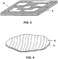
- the layer of plastic 3 comprising the previous metallization layer 4 is imbedded in the reflective surface 1 and can be arranged in strips with a suitable size in order to achieve optimal adaptation to the reflective surface 1 to be metallized, or forming different shapes following determined patterns ( Figures 3, 4 and 5 ).
- the reflective surface 1 can be metallized continuously ( Figures 4 and 5 ), or discontinuously ( Figure 3 ).
- the metallization of the metallized strips forming determined patterns or shapes can be also be removed in order to achieve special effects. When the metallization is discontinuous, it can in turn be periodic or non-periodic.
- the metallized layer 4 is bonded to the composite substrate 2 of the reflective surface 1 by the resin itself of the composite of layer 2, as this metallized layer 4 is imbedded during the process of laminating the composite 2 of the reflective surface 1 itself, thus entering the curing cycle as part of the assembly of the reflective surface 1 (formed by the composite 2 together with the plastic 3 comprising a metallization layer 4).
- the process of the invention comprises the following steps (according to the application, some steps may not be necessary):
- Figure 1 shows how the layers of the different materials are arranged to form the reflective surface 1 with the process of the invention. According to the application, some of these layers may be partially or completely eliminated.
- Figure 2 in turn shows a layer of support plastic 3 on which the previously deposited continuous metallization layer 4 is seen.
- Figure 3 depicts a layer of plastic 3 on which the previously deposited metallization layer 4 can be seen after having partially removed said metallization layer 4 in order to achieve modifying the response of the electromagnetic waves.
- the part which remains metallized (layer 4) can be periodic or not and the patterns can be identical or different in each area.
- This metallized layer 4 could also be a negative image.
- Figure 4 shows a reflective surface 1 comprising metallized layers 4 arranged in the form of strips.
- Figures 5 shows a reflective surface 1 with another type of strips (the strips can have any shape and size), according to another embodiment of the invention.
- Figures 3, 4 and 5 show different embodiments of the arrangement of the metallization layer 4.
- the metallization layer 4 can be arranged between the layers of composite 2 (as shown in Figure 1 ), or in the outer surface of the reflective surface 1 of the antenna, which must have given reflective characteristics (as shown in Figure 2 ).
- the plastic 3 comprising a metallization layer 4 is bonded to the composite 2 in step a) in its preimpregnated state.
- the sheets of the composite 2 and metallized plastic (layers 3+4) assembly are cut in step b) in a suitable manner in order to perform the lamination of step d).
- the resin of the composite of layer 2 is polymerized, and with it, the metallized plastic (layers 3+4) and the composite substrate of layer 2 bond together.
- step d) for the purpose of protecting the metal of the metallization layer 4, the metallized plastic (layers 3+4) is placed with the plastic face (layer 3) arranged outwardly, such that the metallization layer 4 is protected since it is covered by the plastic of layer 3 and is therefore not exposed to the external environment or to possible contamination by contact or by lack of cleaning.
- the adhesion of the metallization layer or metallized layer 4 to the substrate of the composite of layer 2 is better than in the case of glued metallic layers (by means of the vacuum deposition or chemical deposition process), given that, during the entire polymerization process of the resin of the composite in step h), a pressure is maintained (that of the curing cycle) assuring suitable contact between the surfaces to be bonded, the previous adhesion being much better than the adhesion of metal deposition by vacuum or by chemical process, because in the last cases, the adhesion is very dependent on the suitable activation of the surfaces, as well as on the cleaning of the substrate of the composite of layer 2.
- the process of the invention furthermore does not require complex metallization installations as in the known technique, but rather it can be performed in the same installations in which the elements of the composite are manufactured without having to change anything in the installation.
- the process of the invention can be performed using any type of metallized plastic, which involves any type of plastic existing on the market (preferably Kapton, Kapton loaded with any type of material, Polyamide, Polyamide loaded with any type of material) or any type of metal (preferably aluminum, silver or gold).
- the thickness of the metallization layer 4 can be any thickness, ranging from the finest thickness (in the order of 8 microns), to the thickest thickness (in the order of 50 microns or 100 microns).
- the substrate of the composite of layer 2 on which the process of the invention is performed can be of any type of composite in which the resin of said composite is polymerized in the curing process.
- the metallization (metallization layers 4) of the reflective surfaces 1 can be performed continuously (using metallization strips), Figures 4 and 5 , or discontinuously (by means of metallization strips or by means of patterns), Figure 3 .
- the metallization may in turn be periodic or non-periodic.
- Being able to change this metallization in a periodic or non-periodic manner has the advantage of being able to change the electromagnetic characteristics of the reflective surface 1 of the antenna, filtering polarization, filtering frequencies or converting one polarization into another.
- the electromagnetic behavior of said wave in turn changes, thus being able to control said behavior according to the required needs.
Landscapes
- Engineering & Computer Science (AREA)
- Chemical & Material Sciences (AREA)
- Composite Materials (AREA)
- Mechanical Engineering (AREA)
- Manufacturing & Machinery (AREA)
- Physics & Mathematics (AREA)
- Electromagnetism (AREA)
- Aerials With Secondary Devices (AREA)
- Casting Or Compression Moulding Of Plastics Or The Like (AREA)
- Laminated Bodies (AREA)
Description
- The present invention relates to a process for improving the reflectivity of reflective surfaces of antennas, said reflective surfaces being made of a composite.
- An antenna is a device designed for the purpose of emitting or receiving electromagnetic waves towards open space. While a transmitter antenna transforms voltages into electromagnetic waves, a receiver antenna performs the reverse function. The traditional classification of antennas is essentially based on the manner in which the electromagnetic field is distributed in the antenna itself or on the technology used, although classifications can also be made from a more practical point of view, based on their features and technology, their specific uses and their operation.
- In the case of antennas with a reflector, the manner of producing and receiving electromagnetic waves is done through one or more reflective surfaces, also known as reflectors. If a large main reflector and/or large focal distance involving large distances to the focus needs to be used, then one or more secondary reflectors or subreflectors are normally used, apart from the main reflector. Whereas the main reflector reflects the incident radiation towards the primary focus, the secondary reflector or subreflector has one focus in common with the parabolic reflector and forwards the electromagnetic waves to the secondary focus.
- Thus, the present invention relates to reflective elements (main reflector and/or subreflectors) of the antennas on board telecommunications, radar, radiometer, radio telescope and Earth observation satellites, as well as for other applications. When the reflective elements are made of a composite, the loss of reflectivity (reflectivity being the ability of reflective surfaces to reflect the incident radiation thereon) increases as the frequency increases. Therefore, depending on the work frequency of the mentioned antennas, the reflectivity of their reflective surfaces must be high enough so as to not cause losses which unacceptably degrade the features of said antennas.
- In many applications, instead of using metallic materials to construct the reflective surfaces, composites formed by a fiber (carbon, glass, quartz, etc.) and a resin matrix are used. These materials have either an intrinsically low reflectivity (quartz, glass) or a reflectivity which deteriorates to unacceptable values for high frequencies (from 15 GHz or 20 GHz) due to the ohmic losses occurring when carbon fiber is used as a composite, both if this carbon fiber is painted or unpainted, it being necessary to consider solutions improving the reflectivity of these surfaces.
- One of the processes used today for improving the reflectivity of antenna reflectors made of a composite consists of arranging a metallized layer (process referred to as metallization) on said reflectors. The reduction in the loss of reflectivity is a function of the temperature, of the purity of the metallized layer and of the thickness thereof.
- Multiple methods of metallization are known which can be applied to components manufactured of composites, as is the case of antenna reflectors, particularly for satellites. These methods can be included in three groups: physical methods, chemical methods and others.
- The physical methods can in turn be sub-divided into two groups: metal spraying processes and vacuum deposition processes. The metal spraying can in turn be performed by several techniques (flame spraying, electro spraying and plasma spraying). They all essentially consist of raising the temperature of the metal to be deposited above the melting temperature thereof, subsequently projecting the resulting particles by means of special guns. Vacuum deposition can also use several techniques (vaporization, sputtering and ion plating), atoms of metal or vaporized metal being deposited in all of them on the substrate to be metallized in a vacuum environment.
- The chemical methods in turn include several processes, such as auto-catalytic coating, electrodeposition and chemical vapor deposition. Auto-catalytic coating consists of activating the surfaces to be metallized such that metal ions generated in a solution prepared for such purpose are deposited thereon. Electrodeposition consists of depositing a metal on a surface upon passing a current in a bath in which the surface to be metallized is introduced.
- Within other methods processes not covered by the previous classifications are considered, such as gluing thin sheets of metal either continuously or in strips.
- Out of all the mentioned methods, the method which has been used in spatial applications, specifically for satellites, until now has been the vacuum deposition method. This technique has, however, serious drawbacks and limitations, as it is an expensive technique requiring the use of very sophisticated installations, there being virtually no installations of this type for large sizes, the few existing installations furthermore being non-industrial, rather being of a scientific institution, which has limited their use to very specific cases, such as that of telescope mirrors on board satellites.
- In addition, the vacuum deposition metallization technique commonly used, in which the material with elevated conductivity is mainly aluminum, produces very thin and very sensitive metallization depositions arranged on the outer face of the surfaces, these metallization layers being very easily damaged, even when cleaning the surfaces, the metallization layer in many cases being removed when the process of cleaning said surfaces is performed. In the event that the metallization layer is damaged, it is necessary to remove the entire arranged layer and again perform the metallization process once more, which involves a very high cost.
- It is known in the state of the art, as per document
WO 2008/071922 A1 , a method of manufacturing a composite and of securing a metallic coating to a resin-based composite material, comprising a keying structure interlocking with the composite material. It is also known fromJP 02154499 a JP 01184999 US 2003/0102077 A1 . - The present invention is aimed at solving the previously mentioned drawbacks.
- Thus, the invention describes a process for improving the reflectivity of reflective surfaces of antennas as defined in the sole
independent claim 1, said reflective surfaces being made of a composite, upon imbedding a layer of metallized dielectric plastic between the layers of composite or in the outer surface of the reflective surface of the antenna which must have given reflective characteristics in the antenna. This layer of metallized dielectric plastic is arranged while laminating the composite that is going to form the mentioned reflective surface. - According to the process of the invention, the layer of metallized plastic which is imbedded in the reflector can be arranged in strips with a suitable size in order to achieve optimal adaptation to the reflective surface to be metallized, or forming different shapes following determined patterns. The reflective surface can then be metallized continuously, i.e., the previous strips being adapted such that they completely cover the entire reflective surface or arranging the previous strips discontinuously, such that they do not completely cover the previous reflective surface, but rather they are only arranged in some determined areas thereof. The metallization of the metallized strips forming determined patterns or shapes can also be removed to achieve special effects. When the metallization is discontinuous (either by means of metallized strips or by means of patterns) it can in turn be periodic or non-periodic.
- These periodic or non-periodic metallization shapes can achieve several effects improving the characteristics of the antennas, such as polarizing the electromagnetic fields, altering their phase and amplitude and, in summary, controlling the radiation diagram of the antenna in a simple manner.
- According to the invention, the metallized layer is bonded to the composite substrate of the reflective surface by the resin itself of the composite, as this metallized layer is imbedded during the process of laminating the composite of the reflective surface itself, thus entering the curing cycle as part of the assembly of the reflective surface (formed by the composite together with the metallized plastic).
- The process of the invention for performing the metallization of reflective surfaces of antennas, particularly for satellites, said reflective surfaces being made of composite, by means of which the reflectivity of said reflective surfaces is improved, upon reducing the losses of reflectivity thereof, comprises the following steps:
- a) laminating the metallized plastic on the composite of the reflective surface;
- b) cutting the assembly of composite and metallized plastic;
- c) forming strips or patterns with a determined shape from the assembly of composite and metallized plastic of step b);
- d) laminating the strips or patterns of step c), formed by the assembly of composite and metallized plastic, as a first layer on the molding jig, the metallized plastic side of the strips or patterns being in contact with the molding jig;
- e) ending the lamination process, adding the rest of the layers of composite of the reflective surface to the first layer made in step d);
- f) preparing the vacuum and curing bag;
- g) introducing the assembly obtained in e) in the autoclave;
- h) performing the curing cycle on the previous assembly, which will be defined by the resin of the composite of the reflective surface.
- Other features and advantages of the present invention will be understood from the following detailed description of an illustrative embodiment of the object of the invention in relation to the attached figures.
-
-
Figure 1 shows how the layers of the different materials are arranged in a metallized reflective surface of an antenna according to a first embodiment of the process of the present invention. -
Figure 2 shows how a continuous metallization layer is arranged on a metallized reflective surface of an antenna according to a second embodiment of the process of the present invention. -
Figure 3 shows a metallized reflective surface of an antenna on which a metallization has been performed, subsequently performing a partial removal thereof in order to achieve modifying the response of the electromagnetic waves, according to a third embodiment of the process of the present invention. -
Figure 4 shows a metallized reflective surface of an antenna comprising strips on which the metallization is arranged, according to a fourth embodiment of the process of the present invention. -
Figure 5 shows a metallized reflective surface of an antenna comprising another type of strips on which the metallization is arranged, according to a fifth embodiment of the process of the present invention. - The invention describes a process for improving the reflectivity of
reflective surfaces 1 of antennas arranged in satellites, saidreflective surfaces 1 being made of a composite. The composite comprises a resin matrix and fibers, these fibers preferably being carbon fibers. According to the process of the invention, a layer of metallizeddielectric plastic 3 is imbedded by means of ametallization layer 4 between the layers of composite 2 (Figure 1 ) or in the outer surface of the reflector of the antenna which must have given reflective characteristics (Figure 2 ). The layer of metallized dielectric plastic 3 (metallized by means of the metallization layer 4) is arranged while laminating the composite which will form the mentioned reflector orreflective surface 1. - The layer of
plastic 3 comprising theprevious metallization layer 4 is imbedded in thereflective surface 1 and can be arranged in strips with a suitable size in order to achieve optimal adaptation to thereflective surface 1 to be metallized, or forming different shapes following determined patterns (Figures 3, 4 and5 ). Thereflective surface 1 can be metallized continuously (Figures 4 and5 ), or discontinuously (Figure 3 ). The metallization of the metallized strips forming determined patterns or shapes can be also be removed in order to achieve special effects. When the metallization is discontinuous, it can in turn be periodic or non-periodic. - The metallized
layer 4 is bonded to thecomposite substrate 2 of thereflective surface 1 by the resin itself of the composite oflayer 2, as thismetallized layer 4 is imbedded during the process of laminating thecomposite 2 of thereflective surface 1 itself, thus entering the curing cycle as part of the assembly of the reflective surface 1 (formed by the composite 2 together with theplastic 3 comprising a metallization layer 4). - The process of the invention comprises the following steps (according to the application, some steps may not be necessary):
- a) laminating the
plastic 3 comprising ametallization layer 4 on thecomposite 2 of thereflective surface 1; - b) cutting the assembly of
composite 2 and metallized plastic (layers 3+4); - c) forming strips or patterns with a determined shape from the assembly of
composite 2 and metallized plastic (layers 3+4) of step b); - d) laminating the strips or patterns of step c), formed by the assembly of
composite 2 and metallized plastic (layers 3+4), as a first layer on the molding jig, the metallized plastic side (layers 3+4) of the strips or patterns being in contact with the molding jig; - e) ending the lamination process, adding the rest of the layers of
composite 2 of thereflective surface 1 to the first layer made in step d); - f) preparing the vacuum and curing bag;
- g) introducing the assembly obtained in e) in the autoclave;
- h) performing the curing cycle of the previous assembly, which will be defined or determined by the resin of the composite of the
reflective surface 1. -
Figure 1 shows how the layers of the different materials are arranged to form thereflective surface 1 with the process of the invention. According to the application, some of these layers may be partially or completely eliminated. -
Figure 2 in turn shows a layer ofsupport plastic 3 on which the previously depositedcontinuous metallization layer 4 is seen. -
Figure 3 depicts a layer ofplastic 3 on which the previously depositedmetallization layer 4 can be seen after having partially removed saidmetallization layer 4 in order to achieve modifying the response of the electromagnetic waves. The part which remains metallized (layer 4) can be periodic or not and the patterns can be identical or different in each area. This metallizedlayer 4 could also be a negative image. -
Figure 4 shows areflective surface 1 comprising metallizedlayers 4 arranged in the form of strips. -
Figures 5 shows areflective surface 1 with another type of strips (the strips can have any shape and size), according to another embodiment of the invention. -
Figures 3, 4 and5 show different embodiments of the arrangement of themetallization layer 4. In all of them, themetallization layer 4 can be arranged between the layers of composite 2 (as shown inFigure 1 ), or in the outer surface of thereflective surface 1 of the antenna, which must have given reflective characteristics (as shown inFigure 2 ). - The
plastic 3 comprising ametallization layer 4 is bonded to the composite 2 in step a) in its preimpregnated state. The sheets of thecomposite 2 and metallized plastic (layers 3+4) assembly are cut in step b) in a suitable manner in order to perform the lamination of step d). - In the curing process defined in the previous step h), the resin of the composite of
layer 2 is polymerized, and with it, the metallized plastic (layers 3+4) and the composite substrate oflayer 2 bond together. - In step d), for the purpose of protecting the metal of the
metallization layer 4, the metallized plastic (layers 3+4) is placed with the plastic face (layer 3) arranged outwardly, such that themetallization layer 4 is protected since it is covered by the plastic oflayer 3 and is therefore not exposed to the external environment or to possible contamination by contact or by lack of cleaning. - The difference of the process defined by the invention with respect to the mentioned known vacuum deposition metallization process, in which strips are glued, is based on the fact that in the invention, the adhesion is not performed by an adhesive which is incorporated as an element for performing the bond, but rather it is the resin itself of the layer of
composite 2 which, upon polymerizing during the curing cycle, bonds the layer of metallized plastic (layers 3+4) to the rest of the substrate of the layer ofcomposite 2. - In the process of the invention, the adhesion of the metallization layer or metallized
layer 4 to the substrate of the composite oflayer 2 is better than in the case of glued metallic layers (by means of the vacuum deposition or chemical deposition process), given that, during the entire polymerization process of the resin of the composite in step h), a pressure is maintained (that of the curing cycle) assuring suitable contact between the surfaces to be bonded, the previous adhesion being much better than the adhesion of metal deposition by vacuum or by chemical process, because in the last cases, the adhesion is very dependent on the suitable activation of the surfaces, as well as on the cleaning of the substrate of the composite oflayer 2. - The process of the invention furthermore does not require complex metallization installations as in the known technique, but rather it can be performed in the same installations in which the elements of the composite are manufactured without having to change anything in the installation.
- Thus, some of the main advantages of the process of the invention are:
- it simplifies the required process, given that it can be performed in the same installations in which the components or surfaces which are going to be metallized are manufactured, thus reducing the manufacturing times, since the components do not have to be transported outside the manufacturing installations for the same, this being a very relevant aspect in this type of products in which delivery times are always very critical;
- it simplifies the required process, given that it is the operator who laminates the composite of the reflective surface who also performs the metallization process of the invention at the same time;
- it improves the adhesion of the metallized
layer 4 to the substrate of the composite of the layer ofcomposite 2; - it assures excellent homogeneity of the metallic layer or
metallization layer 4 obtained by means of the mentioned process; - it assures the protection of the metal of the
metallization layer 4 in the lamination step, as the metallized plastic (layers 3+4) is arranged with the plastic (layer 3) arranged outwardly such that themetallization layer 4 is protected since it is covered by the plastic and is not exposed to the external environment or to possible contamination by contact or by lack of cleaning. - The process of the invention can be performed using any type of metallized plastic, which involves any type of plastic existing on the market (preferably Kapton, Kapton loaded with any type of material, Polyamide, Polyamide loaded with any type of material) or any type of metal (preferably aluminum, silver or gold). Likewise, the thickness of the
metallization layer 4 can be any thickness, ranging from the finest thickness (in the order of 8 microns), to the thickest thickness (in the order of 50 microns or 100 microns). Furthermore, the substrate of the composite oflayer 2 on which the process of the invention is performed can be of any type of composite in which the resin of said composite is polymerized in the curing process. - Another feature of the process of the invention is that the metallization (metallization layers 4) of the
reflective surfaces 1 can be performed continuously (using metallization strips),Figures 4 and5 , or discontinuously (by means of metallization strips or by means of patterns),Figure 3 . When the metallization is discontinuous (Figure 3 ), it may in turn be periodic or non-periodic. Being able to change this metallization in a periodic or non-periodic manner has the advantage of being able to change the electromagnetic characteristics of thereflective surface 1 of the antenna, filtering polarization, filtering frequencies or converting one polarization into another. By changing the polarization of the electromagnetic wave reflected by thereflective surface 1, accordingly the antenna, the electromagnetic behavior of said wave in turn changes, thus being able to control said behavior according to the required needs. - Those modifications comprised within the scope defined by the following claims can be introduced in the preferred embodiments described above.
Claims (12)
- A process for improving the reflectivity of reflective surfaces (1) of antennas, said reflective surfaces (1) being made of a composite comprising a resin matrix and fibers, comprising at least one layer of composite (2), comprising the following steps:a) laminating a layer of plastic (3) comprising a metallization layer (4) on the at least one layer of composite (2), bonding the metallization layer (4) to the substrate of the layer of composite (2) in its preimpregnated state by means of the resin itself of the composite;b) cutting the assembly of the layer of composite (2) and the layer of plastic (3) comprising a metallization layer (4);c) forming strips or patterns with a determined shape from the assembly formed by the layer of composite (2) and the layer of plastic (3) comprising a metallization layer (4) of step b);d) laminating the strips or patterns of step c) as a first layer on a molding jig;e) ending the lamination process, adding the rest of the layers of composite (2) of the reflective surface (1) to the first layer made in step d);f) preparing the vacuum and curing bag;g) introducing in the autoclave;h) performing the curing cycle, in which the resin of the composite, upon polymerizing, bonds the layer of plastic (3) comprising the metallization layer (4) to the rest of the substrate of the layer of composite (2).
- The process for improving the reflectivity of reflective surfaces (1) of antennas according to claim 1, characterized in that in step a), the layer of plastic (3) comprising the metallization layer (4) is arranged between several layers of composite (2).
- The process for improving the reflectivity of reflective surfaces (1) of antennas according to claim 1, characterized in that in step a), the layer of plastic (3) comprising the metallization layer (4) is arranged in the outer surface of the reflective surface (1) of the antenna which must have given reflective characteristics.
- The process for improving the reflectivity of reflective surfaces (1) of antennas according to any of the previous claims, characterized in that in step a), the metallization layer (4) is arranged continuously on the layer of plastic (3).
- The process for improving the reflectivity of reflective surfaces (1) of antennas according to any of claims 1-3, characterized in that in step a), the metallization layer (4) is arranged discontinuously on the layer of plastic (3) in order to achieve modifying the characteristics of the antennas by modifying the response of the electromagnetic waves emitted or received by the antenna.
- The process for improving the reflectivity of reflective surfaces (1) of antennas according to claim 5, characterized in that the discontinuous metallization layer (4) can be periodic or non-periodic.
- The process for improving the reflectivity of reflective surfaces (1) of antennas according to any of the previous claims, characterized in that in step d), the side of the layer of plastic (3) is the one that is in contact with the molding jig, such that the metallization layer (4) is protected since it is covered by the plastic of layer (3) and is therefore not exposed to the external environment or to the possible contamination by contact or by lack of cleaning.
- The process for improving the reflectivity of reflective surfaces (1) of antennas according to any of the previous claims, characterized in that in step h), a pressure is maintained during the entire curing cycle to assure the appropriate bonding of the layer of plastic (3) comprising the metallization layer (4) to the rest of the substrate of the layer of composite (2).
- The process for improving the reflectivity of reflective surfaces (1) of antennas according to any of the previous claims, characterized in that in step h), the curing cycle is determined by the type of resin of the composite.
- The process for improving the reflectivity of reflective surfaces (1) of antennas according to any of the previous claims, characterized in that the composite of the layer of composite (2) comprises a resin matrix and carbon fibers.
- The process for improving the reflectivity of reflective surfaces (1) of antennas according to any of the previous claims, characterized in that the thickness of the metallization layer (4) ranges from the 4 microns to 100
- The process for improving the reflectivity of reflective surfaces (1) of antennas according to any of the previous claims, characterized in that the reflective surfaces (1) are arranged in satellite antennas.
Priority Applications (5)
| Application Number | Priority Date | Filing Date | Title |
|---|---|---|---|
| ES09382071.0T ES2652121T3 (en) | 2009-05-18 | 2009-05-18 | Procedure to improve the reflectivity of antenna reflecting surfaces |
| EP09382071.0A EP2254198B1 (en) | 2009-05-18 | 2009-05-18 | Process for improving the reflectivity of antenna reflecting surfaces |
| CA2704531A CA2704531C (en) | 2009-05-18 | 2010-05-17 | Process for improving the reflectivity of reflective surfaces of antennas |
| JP2010113626A JP5722552B2 (en) | 2009-05-18 | 2010-05-17 | The process of increasing the reflectivity of the reflective surface of the antenna |
| US12/782,491 US8317960B2 (en) | 2009-05-18 | 2010-05-18 | Process for improving the reflectivity of reflective surfaces of antennas |
Applications Claiming Priority (1)
| Application Number | Priority Date | Filing Date | Title |
|---|---|---|---|
| EP09382071.0A EP2254198B1 (en) | 2009-05-18 | 2009-05-18 | Process for improving the reflectivity of antenna reflecting surfaces |
Publications (2)
| Publication Number | Publication Date |
|---|---|
| EP2254198A1 EP2254198A1 (en) | 2010-11-24 |
| EP2254198B1 true EP2254198B1 (en) | 2017-09-27 |
Family
ID=41137197
Family Applications (1)
| Application Number | Title | Priority Date | Filing Date |
|---|---|---|---|
| EP09382071.0A Active EP2254198B1 (en) | 2009-05-18 | 2009-05-18 | Process for improving the reflectivity of antenna reflecting surfaces |
Country Status (5)
| Country | Link |
|---|---|
| US (1) | US8317960B2 (en) |
| EP (1) | EP2254198B1 (en) |
| JP (1) | JP5722552B2 (en) |
| CA (1) | CA2704531C (en) |
| ES (1) | ES2652121T3 (en) |
Families Citing this family (13)
| Publication number | Priority date | Publication date | Assignee | Title |
|---|---|---|---|---|
| CN102157786A (en) * | 2010-12-10 | 2011-08-17 | 中国兵器工业第二○六研究所 | Composite material stripline antenna processing method |
| ITRM20120020A1 (en) | 2012-01-20 | 2013-07-21 | Unilab S A S Di Lavagna Silvio Mas Simo & C | PROCESS TO IMPROVE THE REFLECTIVITY OF REFLECTIVE ANTENNA SURFACES. |
| ITRM20130397A1 (en) | 2013-07-08 | 2015-01-09 | Silvio Massimo Lavagna | METALLIZED REFLECTOR PROCESS FOR HIGH FREQUENCIES. |
| CA2917879A1 (en) | 2013-07-09 | 2015-01-15 | United Technologies Corporation | Metal-encapsulated polymeric article |
| EP3019710A4 (en) | 2013-07-09 | 2017-05-10 | United Technologies Corporation | Plated polymer fan |
| CA2917643A1 (en) * | 2013-07-09 | 2015-01-15 | United Technologies Corporation | Industrial products formed from plated polymers |
| CA2917967A1 (en) | 2013-07-09 | 2015-01-15 | United Technologies Corporation | Plated polymer compressor |
| WO2015017095A2 (en) | 2013-07-09 | 2015-02-05 | United Technologies Corporation | Plated polymer nosecone |
| US9685710B1 (en) | 2014-01-22 | 2017-06-20 | Space Systems/Loral, Llc | Reflective and permeable metalized laminate |
| DE102017222983A1 (en) * | 2017-12-18 | 2019-06-19 | Bayerische Motoren Werke Aktiengesellschaft | Process for producing a fiber composite component |
| US10516216B2 (en) | 2018-01-12 | 2019-12-24 | Eagle Technology, Llc | Deployable reflector antenna system |
| US10707552B2 (en) | 2018-08-21 | 2020-07-07 | Eagle Technology, Llc | Folded rib truss structure for reflector antenna with zero over stretch |
| CN114325613B (en) * | 2021-12-24 | 2023-05-02 | 西南交通大学 | Radar detection power prediction method under regional non-uniform evaporation waveguide |
Family Cites Families (11)
| Publication number | Priority date | Publication date | Assignee | Title |
|---|---|---|---|---|
| JPS6113701A (en) * | 1984-06-29 | 1986-01-22 | Fujitsu Ltd | Production of sandwich type antenna reflector |
| JPS62118611A (en) * | 1985-11-19 | 1987-05-30 | Toshiba Corp | Manufacture of antenna reflection mirror panel |
| JPH01184999A (en) | 1988-01-20 | 1989-07-24 | Bridgestone Corp | Electromagnetic wave reflector |
| JPH02154499A (en) | 1988-12-06 | 1990-06-13 | Bridgestone Corp | Electromagnetic wave reflector |
| JPH0612851B2 (en) * | 1989-06-06 | 1994-02-16 | アロン化成株式会社 | Antenna reflector and method of manufacturing the same |
| JPH04166310A (en) * | 1990-10-30 | 1992-06-12 | Navitas Kk | Manufacture of reflecting plate for antenna |
| JPH05191135A (en) * | 1992-01-08 | 1993-07-30 | Toshiba Corp | Electromagnetic wave reflecting structure and its production |
| US5686172A (en) * | 1994-11-30 | 1997-11-11 | Mitsubishi Gas Chemical Company, Inc. | Metal-foil-clad composite ceramic board and process for the production thereof |
| JP2983451B2 (en) * | 1995-08-24 | 1999-11-29 | 株式会社東芝 | Method of manufacturing reflector |
| US20030102077A1 (en) | 2001-12-03 | 2003-06-05 | Pioneer Technology Engineering Co., Ltd., | Method for manufacturing a copper-clad laminate |
| GB2444710B (en) | 2006-12-14 | 2011-04-13 | Advanced Composites Group Ltd | Metallic coating of composite materials |
-
2009
- 2009-05-18 ES ES09382071.0T patent/ES2652121T3/en active Active
- 2009-05-18 EP EP09382071.0A patent/EP2254198B1/en active Active
-
2010
- 2010-05-17 CA CA2704531A patent/CA2704531C/en active Active
- 2010-05-17 JP JP2010113626A patent/JP5722552B2/en active Active
- 2010-05-18 US US12/782,491 patent/US8317960B2/en active Active
Non-Patent Citations (1)
| Title |
|---|
| None * |
Also Published As
| Publication number | Publication date |
|---|---|
| US8317960B2 (en) | 2012-11-27 |
| EP2254198A1 (en) | 2010-11-24 |
| US20100288433A1 (en) | 2010-11-18 |
| CA2704531C (en) | 2017-06-13 |
| ES2652121T3 (en) | 2018-01-31 |
| CA2704531A1 (en) | 2010-11-18 |
| JP2010268467A (en) | 2010-11-25 |
| JP5722552B2 (en) | 2015-05-20 |
Similar Documents
| Publication | Publication Date | Title |
|---|---|---|
| EP2254198B1 (en) | Process for improving the reflectivity of antenna reflecting surfaces | |
| US9774080B2 (en) | Electromagnetic wave shielding sheet for antenna, method for manufacturing same, antenna comprising same, and battery pack for portable terminal having said antenna | |
| KR101601530B1 (en) | Radio wave penetration type optical film with muiltiple layer | |
| US8665175B2 (en) | Thermal control film for spacecraft | |
| EP1852938A1 (en) | Antenna radome | |
| CN110771274B (en) | Electromagnetic wave absorber and molded article with electromagnetic wave absorber | |
| US11909107B2 (en) | Gradient permittivity film | |
| US9653819B1 (en) | Waveguide antenna fabrication | |
| JP2010268467A5 (en) | ||
| JP2010158035A (en) | Glass antenna, and manufacturing method thereof | |
| JP2021082896A (en) | Electromagnetic frequency selective transmission material and vehicle component | |
| US4585317A (en) | Reflector with attenuating connecting plates | |
| US20190308752A1 (en) | Reflective film assembled on a composite structure | |
| JP5039315B2 (en) | Electromagnetic wave shielding film and manufacturing method thereof | |
| EP0243162B1 (en) | Multi-layered microwave absorber and method of manufacturing the same | |
| CN106383376B (en) | A kind of Infrared stealthy materials | |
| US8163127B2 (en) | Process for manufacturing a packaging material | |
| KR102165274B1 (en) | Electromagnetic wave absorbing composites having thermostability | |
| RU2537515C1 (en) | Multi-layered coating of thin-walled envelope from polymer composite material of space antenna reflector | |
| KR19980071237A (en) | Process for Film Transfer Metallization | |
| US8481153B1 (en) | Apparatus and method for imparting wide angle low reflection on conductive surfaces | |
| EP3766664A1 (en) | Assembly and mounting of a reflective film on a composite structure | |
| US20230202099A1 (en) | 3-d object comprising a sandwich of one or more composite layers, of one or more layers of metal patterns and optionally of one or more layers of possibly dense polymers for electromagnetic applications in antennas and/or radomes | |
| JPH0661679A (en) | Thin radio wave absorbent | |
| JP2000174545A (en) | Transparent radio wave absorbing sheet |
Legal Events
| Date | Code | Title | Description |
|---|---|---|---|
| PUAI | Public reference made under article 153(3) epc to a published international application that has entered the european phase |
Free format text: ORIGINAL CODE: 0009012 |
|
| AK | Designated contracting states |
Kind code of ref document: A1 Designated state(s): AT BE BG CH CY CZ DE DK EE ES FI FR GB GR HR HU IE IS IT LI LT LU LV MC MK MT NL NO PL PT RO SE SI SK TR |
|
| AX | Request for extension of the european patent |
Extension state: AL BA RS |
|
| RIN1 | Information on inventor provided before grant (corrected) |
Inventor name: MONTESANO BENITO, CARLOS ENRIQUE Inventor name: OZORES MONGE, EDUARDO |
|
| RTI1 | Title (correction) |
Free format text: PROCESS FOR IMPROVING THE REFLECTIVITY OF ANTENNA REFLECTING SURFACES |
|
| 17P | Request for examination filed |
Effective date: 20110511 |
|
| 17Q | First examination report despatched |
Effective date: 20110527 |
|
| REG | Reference to a national code |
Ref country code: DE Ref legal event code: R079 Ref document number: 602009048541 Country of ref document: DE Free format text: PREVIOUS MAIN CLASS: H01Q0015140000 Ipc: B29C0070440000 |
|
| GRAP | Despatch of communication of intention to grant a patent |
Free format text: ORIGINAL CODE: EPIDOSNIGR1 |
|
| STAA | Information on the status of an ep patent application or granted ep patent |
Free format text: STATUS: GRANT OF PATENT IS INTENDED |
|
| RIC1 | Information provided on ipc code assigned before grant |
Ipc: B32B 38/10 20060101ALN20170320BHEP Ipc: B29C 70/44 20060101AFI20170320BHEP Ipc: B29C 70/88 20060101ALI20170320BHEP Ipc: B32B 38/00 20060101ALI20170320BHEP Ipc: H01Q 15/14 20060101ALI20170320BHEP Ipc: B29C 70/08 20060101ALI20170320BHEP |
|
| RIC1 | Information provided on ipc code assigned before grant |
Ipc: B29C 70/88 20060101ALI20170328BHEP Ipc: B29C 70/44 20060101AFI20170328BHEP Ipc: B32B 38/10 20060101ALN20170328BHEP Ipc: B32B 38/00 20060101ALI20170328BHEP Ipc: B29C 70/08 20060101ALI20170328BHEP Ipc: H01Q 15/14 20060101ALI20170328BHEP |
|
| INTG | Intention to grant announced |
Effective date: 20170411 |
|
| GRAS | Grant fee paid |
Free format text: ORIGINAL CODE: EPIDOSNIGR3 |
|
| GRAA | (expected) grant |
Free format text: ORIGINAL CODE: 0009210 |
|
| STAA | Information on the status of an ep patent application or granted ep patent |
Free format text: STATUS: THE PATENT HAS BEEN GRANTED |
|
| RAP1 | Party data changed (applicant data changed or rights of an application transferred) |
Owner name: AIRBUS DEFENCE AND SPACE, S.A. |
|
| AK | Designated contracting states |
Kind code of ref document: B1 Designated state(s): AT BE BG CH CY CZ DE DK EE ES FI FR GB GR HR HU IE IS IT LI LT LU LV MC MK MT NL NO PL PT RO SE SI SK TR |
|
| REG | Reference to a national code |
Ref country code: GB Ref legal event code: FG4D |
|
| REG | Reference to a national code |
Ref country code: CH Ref legal event code: EP |
|
| REG | Reference to a national code |
Ref country code: AT Ref legal event code: REF Ref document number: 931582 Country of ref document: AT Kind code of ref document: T Effective date: 20171015 |
|
| REG | Reference to a national code |
Ref country code: IE Ref legal event code: FG4D |
|
| REG | Reference to a national code |
Ref country code: DE Ref legal event code: R096 Ref document number: 602009048541 Country of ref document: DE |
|
| REG | Reference to a national code |
Ref country code: SE Ref legal event code: TRGR |
|
| REG | Reference to a national code |
Ref country code: NL Ref legal event code: FP |
|
| PG25 | Lapsed in a contracting state [announced via postgrant information from national office to epo] |
Ref country code: HR Free format text: LAPSE BECAUSE OF FAILURE TO SUBMIT A TRANSLATION OF THE DESCRIPTION OR TO PAY THE FEE WITHIN THE PRESCRIBED TIME-LIMIT Effective date: 20170927 Ref country code: NO Free format text: LAPSE BECAUSE OF FAILURE TO SUBMIT A TRANSLATION OF THE DESCRIPTION OR TO PAY THE FEE WITHIN THE PRESCRIBED TIME-LIMIT Effective date: 20171227 Ref country code: LT Free format text: LAPSE BECAUSE OF FAILURE TO SUBMIT A TRANSLATION OF THE DESCRIPTION OR TO PAY THE FEE WITHIN THE PRESCRIBED TIME-LIMIT Effective date: 20170927 Ref country code: FI Free format text: LAPSE BECAUSE OF FAILURE TO SUBMIT A TRANSLATION OF THE DESCRIPTION OR TO PAY THE FEE WITHIN THE PRESCRIBED TIME-LIMIT Effective date: 20170927 |
|
| REG | Reference to a national code |
Ref country code: ES Ref legal event code: FG2A Ref document number: 2652121 Country of ref document: ES Kind code of ref document: T3 Effective date: 20180131 |
|
| REG | Reference to a national code |
Ref country code: LT Ref legal event code: MG4D |
|
| PG25 | Lapsed in a contracting state [announced via postgrant information from national office to epo] |
Ref country code: GR Free format text: LAPSE BECAUSE OF FAILURE TO SUBMIT A TRANSLATION OF THE DESCRIPTION OR TO PAY THE FEE WITHIN THE PRESCRIBED TIME-LIMIT Effective date: 20171228 Ref country code: BG Free format text: LAPSE BECAUSE OF FAILURE TO SUBMIT A TRANSLATION OF THE DESCRIPTION OR TO PAY THE FEE WITHIN THE PRESCRIBED TIME-LIMIT Effective date: 20171227 Ref country code: LV Free format text: LAPSE BECAUSE OF FAILURE TO SUBMIT A TRANSLATION OF THE DESCRIPTION OR TO PAY THE FEE WITHIN THE PRESCRIBED TIME-LIMIT Effective date: 20170927 |
|
| PG25 | Lapsed in a contracting state [announced via postgrant information from national office to epo] |
Ref country code: RO Free format text: LAPSE BECAUSE OF FAILURE TO SUBMIT A TRANSLATION OF THE DESCRIPTION OR TO PAY THE FEE WITHIN THE PRESCRIBED TIME-LIMIT Effective date: 20170927 Ref country code: CZ Free format text: LAPSE BECAUSE OF FAILURE TO SUBMIT A TRANSLATION OF THE DESCRIPTION OR TO PAY THE FEE WITHIN THE PRESCRIBED TIME-LIMIT Effective date: 20170927 |
|
| REG | Reference to a national code |
Ref country code: FR Ref legal event code: PLFP Year of fee payment: 10 |
|
| PG25 | Lapsed in a contracting state [announced via postgrant information from national office to epo] |
Ref country code: EE Free format text: LAPSE BECAUSE OF FAILURE TO SUBMIT A TRANSLATION OF THE DESCRIPTION OR TO PAY THE FEE WITHIN THE PRESCRIBED TIME-LIMIT Effective date: 20170927 Ref country code: IS Free format text: LAPSE BECAUSE OF FAILURE TO SUBMIT A TRANSLATION OF THE DESCRIPTION OR TO PAY THE FEE WITHIN THE PRESCRIBED TIME-LIMIT Effective date: 20180127 Ref country code: SK Free format text: LAPSE BECAUSE OF FAILURE TO SUBMIT A TRANSLATION OF THE DESCRIPTION OR TO PAY THE FEE WITHIN THE PRESCRIBED TIME-LIMIT Effective date: 20170927 |
|
| REG | Reference to a national code |
Ref country code: DE Ref legal event code: R097 Ref document number: 602009048541 Country of ref document: DE |
|
| PG25 | Lapsed in a contracting state [announced via postgrant information from national office to epo] |
Ref country code: DK Free format text: LAPSE BECAUSE OF FAILURE TO SUBMIT A TRANSLATION OF THE DESCRIPTION OR TO PAY THE FEE WITHIN THE PRESCRIBED TIME-LIMIT Effective date: 20170927 |
|
| PLBE | No opposition filed within time limit |
Free format text: ORIGINAL CODE: 0009261 |
|
| STAA | Information on the status of an ep patent application or granted ep patent |
Free format text: STATUS: NO OPPOSITION FILED WITHIN TIME LIMIT |
|
| PG25 | Lapsed in a contracting state [announced via postgrant information from national office to epo] |
Ref country code: PL Free format text: LAPSE BECAUSE OF FAILURE TO SUBMIT A TRANSLATION OF THE DESCRIPTION OR TO PAY THE FEE WITHIN THE PRESCRIBED TIME-LIMIT Effective date: 20170927 |
|
| 26N | No opposition filed |
Effective date: 20180628 |
|
| PG25 | Lapsed in a contracting state [announced via postgrant information from national office to epo] |
Ref country code: SI Free format text: LAPSE BECAUSE OF FAILURE TO SUBMIT A TRANSLATION OF THE DESCRIPTION OR TO PAY THE FEE WITHIN THE PRESCRIBED TIME-LIMIT Effective date: 20170927 |
|
| PG25 | Lapsed in a contracting state [announced via postgrant information from national office to epo] |
Ref country code: MC Free format text: LAPSE BECAUSE OF FAILURE TO SUBMIT A TRANSLATION OF THE DESCRIPTION OR TO PAY THE FEE WITHIN THE PRESCRIBED TIME-LIMIT Effective date: 20170927 |
|
| REG | Reference to a national code |
Ref country code: IE Ref legal event code: MM4A |
|
| PG25 | Lapsed in a contracting state [announced via postgrant information from national office to epo] |
Ref country code: IE Free format text: LAPSE BECAUSE OF NON-PAYMENT OF DUE FEES Effective date: 20180518 |
|
| PG25 | Lapsed in a contracting state [announced via postgrant information from national office to epo] |
Ref country code: MT Free format text: LAPSE BECAUSE OF NON-PAYMENT OF DUE FEES Effective date: 20180518 |
|
| PG25 | Lapsed in a contracting state [announced via postgrant information from national office to epo] |
Ref country code: TR Free format text: LAPSE BECAUSE OF FAILURE TO SUBMIT A TRANSLATION OF THE DESCRIPTION OR TO PAY THE FEE WITHIN THE PRESCRIBED TIME-LIMIT Effective date: 20170927 |
|
| PG25 | Lapsed in a contracting state [announced via postgrant information from national office to epo] |
Ref country code: PT Free format text: LAPSE BECAUSE OF FAILURE TO SUBMIT A TRANSLATION OF THE DESCRIPTION OR TO PAY THE FEE WITHIN THE PRESCRIBED TIME-LIMIT Effective date: 20170927 Ref country code: HU Free format text: LAPSE BECAUSE OF FAILURE TO SUBMIT A TRANSLATION OF THE DESCRIPTION OR TO PAY THE FEE WITHIN THE PRESCRIBED TIME-LIMIT; INVALID AB INITIO Effective date: 20090518 |
|
| PG25 | Lapsed in a contracting state [announced via postgrant information from national office to epo] |
Ref country code: CY Free format text: LAPSE BECAUSE OF FAILURE TO SUBMIT A TRANSLATION OF THE DESCRIPTION OR TO PAY THE FEE WITHIN THE PRESCRIBED TIME-LIMIT Effective date: 20170927 Ref country code: MK Free format text: LAPSE BECAUSE OF NON-PAYMENT OF DUE FEES Effective date: 20170927 |
|
| REG | Reference to a national code |
Ref country code: AT Ref legal event code: UEP Ref document number: 931582 Country of ref document: AT Kind code of ref document: T Effective date: 20170927 |
|
| PGFP | Annual fee paid to national office [announced via postgrant information from national office to epo] |
Ref country code: LU Payment date: 20240522 Year of fee payment: 16 |
|
| PGFP | Annual fee paid to national office [announced via postgrant information from national office to epo] |
Ref country code: NL Payment date: 20240521 Year of fee payment: 16 |
|
| PGFP | Annual fee paid to national office [announced via postgrant information from national office to epo] |
Ref country code: GB Payment date: 20240521 Year of fee payment: 16 |
|
| PGFP | Annual fee paid to national office [announced via postgrant information from national office to epo] |
Ref country code: DE Payment date: 20240521 Year of fee payment: 16 |
|
| PGFP | Annual fee paid to national office [announced via postgrant information from national office to epo] |
Ref country code: CH Payment date: 20240602 Year of fee payment: 16 |
|
| PGFP | Annual fee paid to national office [announced via postgrant information from national office to epo] |
Ref country code: ES Payment date: 20240626 Year of fee payment: 16 |
|
| PGFP | Annual fee paid to national office [announced via postgrant information from national office to epo] |
Ref country code: AT Payment date: 20240522 Year of fee payment: 16 |
|
| PGFP | Annual fee paid to national office [announced via postgrant information from national office to epo] |
Ref country code: FR Payment date: 20240529 Year of fee payment: 16 |
|
| PGFP | Annual fee paid to national office [announced via postgrant information from national office to epo] |
Ref country code: SE Payment date: 20240521 Year of fee payment: 16 Ref country code: BE Payment date: 20240521 Year of fee payment: 16 |
|
| PGFP | Annual fee paid to national office [announced via postgrant information from national office to epo] |
Ref country code: IT Payment date: 20240524 Year of fee payment: 16 |