EP2254161A2 - Photodiode a controle de charge d'interface et procede associe. - Google Patents
Photodiode a controle de charge d'interface et procede associe. Download PDFInfo
- Publication number
- EP2254161A2 EP2254161A2 EP10162979A EP10162979A EP2254161A2 EP 2254161 A2 EP2254161 A2 EP 2254161A2 EP 10162979 A EP10162979 A EP 10162979A EP 10162979 A EP10162979 A EP 10162979A EP 2254161 A2 EP2254161 A2 EP 2254161A2
- Authority
- EP
- European Patent Office
- Prior art keywords
- layer
- photodiode
- doped layer
- doped
- protective layer
- Prior art date
- Legal status (The legal status is an assumption and is not a legal conclusion. Google has not performed a legal analysis and makes no representation as to the accuracy of the status listed.)
- Withdrawn
Links
- 238000000034 method Methods 0.000 title claims description 7
- 239000010410 layer Substances 0.000 claims abstract description 78
- 239000011241 protective layer Substances 0.000 claims abstract description 33
- 238000002955 isolation Methods 0.000 claims abstract description 25
- 239000000463 material Substances 0.000 claims description 18
- 229910052710 silicon Inorganic materials 0.000 claims description 13
- 239000010703 silicon Substances 0.000 claims description 11
- 238000004519 manufacturing process Methods 0.000 claims description 9
- 229910018072 Al 2 O 3 Inorganic materials 0.000 claims description 8
- 229910016569 AlF 3 Inorganic materials 0.000 claims description 7
- 229910004298 SiO 2 Inorganic materials 0.000 claims description 7
- 238000002513 implantation Methods 0.000 claims description 7
- 239000012212 insulator Substances 0.000 claims description 4
- 238000005530 etching Methods 0.000 claims description 2
- XUIMIQQOPSSXEZ-UHFFFAOYSA-N Silicon Chemical compound [Si] XUIMIQQOPSSXEZ-UHFFFAOYSA-N 0.000 description 12
- 230000000694 effects Effects 0.000 description 11
- 238000000151 deposition Methods 0.000 description 4
- 230000008021 deposition Effects 0.000 description 4
- 238000009413 insulation Methods 0.000 description 4
- 230000006798 recombination Effects 0.000 description 4
- 238000005215 recombination Methods 0.000 description 4
- 239000011810 insulating material Substances 0.000 description 3
- 238000002161 passivation Methods 0.000 description 3
- 239000004065 semiconductor Substances 0.000 description 3
- VYPSYNLAJGMNEJ-UHFFFAOYSA-N Silicium dioxide Chemical compound O=[Si]=O VYPSYNLAJGMNEJ-UHFFFAOYSA-N 0.000 description 2
- 230000015572 biosynthetic process Effects 0.000 description 2
- 230000005684 electric field Effects 0.000 description 2
- 238000005286 illumination Methods 0.000 description 2
- 239000011159 matrix material Substances 0.000 description 2
- 238000004377 microelectronic Methods 0.000 description 2
- 150000004767 nitrides Chemical class 0.000 description 2
- 230000035945 sensitivity Effects 0.000 description 2
- 239000007787 solid Substances 0.000 description 2
- 230000007847 structural defect Effects 0.000 description 2
- 229910052581 Si3N4 Inorganic materials 0.000 description 1
- 238000010521 absorption reaction Methods 0.000 description 1
- 239000000956 alloy Substances 0.000 description 1
- 229910045601 alloy Inorganic materials 0.000 description 1
- AYKIYLNKEPAHBG-UHFFFAOYSA-K aluminum dioxosilane trifluoride Chemical compound [Si](=O)=O.[F-].[Al+3].[F-].[F-] AYKIYLNKEPAHBG-UHFFFAOYSA-K 0.000 description 1
- 230000003667 anti-reflective effect Effects 0.000 description 1
- 230000009286 beneficial effect Effects 0.000 description 1
- 239000002800 charge carrier Substances 0.000 description 1
- 150000001875 compounds Chemical class 0.000 description 1
- 230000003247 decreasing effect Effects 0.000 description 1
- 230000001419 dependent effect Effects 0.000 description 1
- 238000006073 displacement reaction Methods 0.000 description 1
- 230000005670 electromagnetic radiation Effects 0.000 description 1
- 238000005516 engineering process Methods 0.000 description 1
- 239000011229 interlayer Substances 0.000 description 1
- 238000010884 ion-beam technique Methods 0.000 description 1
- 239000002184 metal Substances 0.000 description 1
- 229910052751 metal Inorganic materials 0.000 description 1
- 238000003801 milling Methods 0.000 description 1
- 238000001020 plasma etching Methods 0.000 description 1
- 238000002360 preparation method Methods 0.000 description 1
- 230000001681 protective effect Effects 0.000 description 1
- 235000012239 silicon dioxide Nutrition 0.000 description 1
- 239000000377 silicon dioxide Substances 0.000 description 1
- HQVNEWCFYHHQES-UHFFFAOYSA-N silicon nitride Chemical compound N12[Si]34N5[Si]62N3[Si]51N64 HQVNEWCFYHHQES-UHFFFAOYSA-N 0.000 description 1
- 238000004544 sputter deposition Methods 0.000 description 1
- 235000012431 wafers Nutrition 0.000 description 1
- 229910003158 γ-Al2O3 Inorganic materials 0.000 description 1
Images



Classifications
-
- H—ELECTRICITY
- H10—SEMICONDUCTOR DEVICES; ELECTRIC SOLID-STATE DEVICES NOT OTHERWISE PROVIDED FOR
- H10F—INORGANIC SEMICONDUCTOR DEVICES SENSITIVE TO INFRARED RADIATION, LIGHT, ELECTROMAGNETIC RADIATION OF SHORTER WAVELENGTH OR CORPUSCULAR RADIATION
- H10F30/00—Individual radiation-sensitive semiconductor devices in which radiation controls the flow of current through the devices, e.g. photodetectors
- H10F30/20—Individual radiation-sensitive semiconductor devices in which radiation controls the flow of current through the devices, e.g. photodetectors the devices having potential barriers, e.g. phototransistors
- H10F30/21—Individual radiation-sensitive semiconductor devices in which radiation controls the flow of current through the devices, e.g. photodetectors the devices having potential barriers, e.g. phototransistors the devices being sensitive to infrared, visible or ultraviolet radiation
- H10F30/22—Individual radiation-sensitive semiconductor devices in which radiation controls the flow of current through the devices, e.g. photodetectors the devices having potential barriers, e.g. phototransistors the devices being sensitive to infrared, visible or ultraviolet radiation the devices having only one potential barrier, e.g. photodiodes
-
- H—ELECTRICITY
- H10—SEMICONDUCTOR DEVICES; ELECTRIC SOLID-STATE DEVICES NOT OTHERWISE PROVIDED FOR
- H10F—INORGANIC SEMICONDUCTOR DEVICES SENSITIVE TO INFRARED RADIATION, LIGHT, ELECTROMAGNETIC RADIATION OF SHORTER WAVELENGTH OR CORPUSCULAR RADIATION
- H10F71/00—Manufacture or treatment of devices covered by this subclass
- H10F71/121—The active layers comprising only Group IV materials
-
- H—ELECTRICITY
- H10—SEMICONDUCTOR DEVICES; ELECTRIC SOLID-STATE DEVICES NOT OTHERWISE PROVIDED FOR
- H10F—INORGANIC SEMICONDUCTOR DEVICES SENSITIVE TO INFRARED RADIATION, LIGHT, ELECTROMAGNETIC RADIATION OF SHORTER WAVELENGTH OR CORPUSCULAR RADIATION
- H10F77/00—Constructional details of devices covered by this subclass
- H10F77/10—Semiconductor bodies
- H10F77/14—Shape of semiconductor bodies; Shapes, relative sizes or dispositions of semiconductor regions within semiconductor bodies
-
- H—ELECTRICITY
- H10—SEMICONDUCTOR DEVICES; ELECTRIC SOLID-STATE DEVICES NOT OTHERWISE PROVIDED FOR
- H10F—INORGANIC SEMICONDUCTOR DEVICES SENSITIVE TO INFRARED RADIATION, LIGHT, ELECTROMAGNETIC RADIATION OF SHORTER WAVELENGTH OR CORPUSCULAR RADIATION
- H10F39/00—Integrated devices, or assemblies of multiple devices, comprising at least one element covered by group H10F30/00, e.g. radiation detectors comprising photodiode arrays
- H10F39/10—Integrated devices
- H10F39/107—Integrated devices having multiple elements covered by H10F30/00 in a repetitive configuration, e.g. radiation detectors comprising photodiode arrays
-
- H—ELECTRICITY
- H10—SEMICONDUCTOR DEVICES; ELECTRIC SOLID-STATE DEVICES NOT OTHERWISE PROVIDED FOR
- H10F—INORGANIC SEMICONDUCTOR DEVICES SENSITIVE TO INFRARED RADIATION, LIGHT, ELECTROMAGNETIC RADIATION OF SHORTER WAVELENGTH OR CORPUSCULAR RADIATION
- H10F39/00—Integrated devices, or assemblies of multiple devices, comprising at least one element covered by group H10F30/00, e.g. radiation detectors comprising photodiode arrays
- H10F39/80—Constructional details of image sensors
- H10F39/807—Pixel isolation structures
-
- Y—GENERAL TAGGING OF NEW TECHNOLOGICAL DEVELOPMENTS; GENERAL TAGGING OF CROSS-SECTIONAL TECHNOLOGIES SPANNING OVER SEVERAL SECTIONS OF THE IPC; TECHNICAL SUBJECTS COVERED BY FORMER USPC CROSS-REFERENCE ART COLLECTIONS [XRACs] AND DIGESTS
- Y02—TECHNOLOGIES OR APPLICATIONS FOR MITIGATION OR ADAPTATION AGAINST CLIMATE CHANGE
- Y02E—REDUCTION OF GREENHOUSE GAS [GHG] EMISSIONS, RELATED TO ENERGY GENERATION, TRANSMISSION OR DISTRIBUTION
- Y02E10/00—Energy generation through renewable energy sources
- Y02E10/50—Photovoltaic [PV] energy
- Y02E10/547—Monocrystalline silicon PV cells
-
- Y—GENERAL TAGGING OF NEW TECHNOLOGICAL DEVELOPMENTS; GENERAL TAGGING OF CROSS-SECTIONAL TECHNOLOGIES SPANNING OVER SEVERAL SECTIONS OF THE IPC; TECHNICAL SUBJECTS COVERED BY FORMER USPC CROSS-REFERENCE ART COLLECTIONS [XRACs] AND DIGESTS
- Y02—TECHNOLOGIES OR APPLICATIONS FOR MITIGATION OR ADAPTATION AGAINST CLIMATE CHANGE
- Y02P—CLIMATE CHANGE MITIGATION TECHNOLOGIES IN THE PRODUCTION OR PROCESSING OF GOODS
- Y02P70/00—Climate change mitigation technologies in the production process for final industrial or consumer products
- Y02P70/50—Manufacturing or production processes characterised by the final manufactured product
Definitions
- the invention relates to the field of photodiodes and more particularly to photodiodes made in matrices.
- Photodiode technology is based on two important parameters.
- the first parameter is the sensitivity of the photodiode which represents the capacity of the photodiode to collect photogenerated charge carriers. This parameter controls the intensity of the current generated for a given illumination.
- the second parameter is the dark current which represents the current flowing in the photodiode when no light illuminates it. This parameter controls the difference in intensity of the current generated for a given illumination difference.
- a greater or lesser part of the electrons generated in the photodiode do not participate in the photocurrent because they are trapped by structural defects or recombination zones.
- deep isolation trenches are used to limit the effects of neighborhoods.
- deep isolation trenches can play a role similar to structural defects or recombination centers.
- the deep isolation trenches generally comprise an insulating material and are made in a semiconductor medium.
- a property inherent to the silicon / oxide or silicon / nitride interfaces is to have a positive surface charge capable of attracting the photogenerated electrons. It is understandable then that deep isolation trenches act as traps for photogenerated electrons.
- SiN / SiC H passivation layers for p and n type Si wafers
- U. Coscia et al., Thin Solid Films 516 (2008) 1569 describes the effects of surface charges of some materials used for passivation in microelectronics. Particularly mentioned are Al / SiN x / Si, Al / a-SiC x : H / Si and Al / SiN x / a-SiC x : H / Si structures.
- the deep isolation trenches may exhibit recombination effects between the photogenerated electrons and the charges at the interface between the deep isolation trenches and the silicon in a photodiode.
- a photodiode comprising a first doped layer and a second doped layer having a common face, at least one isolation trench. deep region having a face contiguous with the first doped layer and the second doped layer, a free face of the second doped layer being in contact with a conductive layer.
- the photodiode thus defined comprises at least one deep isolation trench being provided on its surface with a protective layer capable of generating a layer of negative charges at the interface with the first doped layer and the second layer. doped and on the other hand the deep isolation trench.
- the photodiode may further comprise an intermediate protective layer located at least partly in the second doped layer, said intermediate protective layer being able to generate a negative charge layer at the interface with the second doped layer.
- the thickness of the intermediate protective layer may be between 5 nm and 20 nm.
- the protective interlayer may be made of a material selected from AlF 3 , SiN / SiC, Al 2 O 3 , HfAl x O y / SiO 2 , AlN with F and ZrO 2 implantation.
- the thickness of the protective layer may be between 5 nm and 20 nm.
- the protective layer may be made of a material selected from AlF 3 , SiN / SiC, Al 2 O 3 , HfAl x O y / SiO 2 , AlN with F and ZrO 2 implantation.
- the protective layer can be made with a thickness of between 5 nm and 20 nm.
- the protective layer may be made of a material selected from AlF 3 , SiN / SiC, Al 2 O 3 , HfAl x O y / SiO 2 , AlN with implantation of F and ZrO 2 .
- the photodiode 1 comprises an opening on a stack of two opposing doping layers forming a diode.
- a first layer 2 has N doping while the second layer 3 has P doping.
- a conductive zone 5 Under the second layer 3 is a conductive zone 5, which may be a silicon layer, a doped silicon layer, or a metal layer.
- the photodiode 1 thus described is generally intended to be integrated in a matrix sensor. It is then necessary to isolate a given photodiode from neighboring photodiodes. For this purpose, deep isolation trenches 4 are formed to separate two immediately adjacent photodiodes. Deep isolation trenches 4 (DTI or "Deep trench insulation” in English) are made of insulating material.
- a space charge area in which the incident electromagnetic radiation can be absorbed. Absorption then gives rise to the creation of an electron-hole pair.
- the electron and the hole each migrate in an opposite direction under the effect of the electric field prevailing in the space charge zone. The displacement of electrons and photogenerated holes thus gives rise to the creation of a photoelectric current.
- deep isolation trenches 4 are generally made of oxide or nitride insulators which have the property of generating a positive charge at the interface with a semiconductor.
- a positive charge layer can generate a field sufficient to attract and capture the photogenerated electrons, thereby decreasing the photoelectric current.
- a first embodiment, illustrated by the figure 2 comprises a protective layer 7.
- This protective layer creates a layer of negative charges at the interface with the first layer 2 and the second layer 3 in order to repel the photogenerated electrons and reduce the risk of capture.
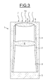
- a second embodiment is illustrated by the figure 3 .
- the second embodiment comprises the development of an intermediate protective layer 8 made of a material similar to the material used in the production of protective layers 7. Such a layer has several beneficial effects on the performance of the photodiode.
- a first effect is to reduce the extension of the space charge area without reducing the potential difference. This has the effect of increasing the electric field to which the pairs are subjected photogenerated electron-hole. The transit time of the electrons and photogenic holes is thus reduced, the response time of the photodiode is improved.
- a second effect is to act as a trap for photogenerated holes, thereby increasing the sensitivity of the photodiode and reducing the dark current of the photodiode.
- this second embodiment is dependent on the depth at which the intermediate protection layer 8 is to be implanted.
- the shorter the wavelength of the incident wave the more the photoelectric effect takes place near the active layer. This implies that the shorter the wavelength, the more it is possible to create an intermediate protection layer 8 close to the active zone.
- the second embodiment is restricted to photodiodes corresponding to the blue pixels in a red, green, blue system.
- the protective layer 7 are made with a thickness of between 5 and 20 nm.
- the protective layer 7 is made of a material selected from AlF 3 , SiN / SiC, Al 2 O 3 , HfAl x O y / SiO 2 , AlN with F and ZrO 2 implantation.
- the protective layer 7 is made during the preparation of the deep isolation trench. Deep isolation trenches are used to physically separate arrayed photodiodes or a photodiode from its immediate environment. For this, trenches are made in the doped silicon forming the first layer 2 and the second layer 3, during an initial step 9 of a manufacturing process. These trenches can be made by wet attack, physical attack of the reactive ion etching type, or ion beam milling.
- a first compliant deposit is made, in a subsequent step 10 of the manufacturing process, to create the protective layer 7.
- a material chosen from AlF 3 , SiN / SiC is deposited.
- the deposition can be carried out by sputtering, by galvanic deposition or by any other method appropriate.
- the conformal deposit provides a constant thickness of material ensuring a consistent effect over the entire length of the deep isolation trench. The thickness obtained is between 5 nm and 20 nm.
- An insulation deposit such as silicon dioxide or silicon nitride, is then made in a subsequent step 11 of the manufacturing process in order to fill the slice and to give it its insulating nature. Subsequent process steps can then be performed, such as the formation of the contact electrodes or the deposition of anti-reflective material.
- the development of the second doped layer 3 is stopped when the thickness reached corresponds to the thickness of the portion located under the intermediate protective layer.
- a layer of the same material is then deposited as the material used to obtain the protective layer 7.
- the desired thickness is reached, the development of the second doped layer and more generally of the photodiode, can resume.
- a photodiode comprising deep isolation trenches has its improved characteristics by inserting a protective layer so that a negative charge area appears at the interface between the silicon and the deep isolation trench.
- an intermediate protective layer can be used to create a negative charge layer at a distance from the active area greater than the distance between the active area and the space charge area.
Landscapes
- Light Receiving Elements (AREA)
- Solid State Image Pick-Up Elements (AREA)
- Element Separation (AREA)
Abstract
Description
- L'invention se rapporte au domaine des photodiodes et plus particulièrement aux photodiodes réalisées en matrices.
- La technologie des photodiodes repose sur deux paramètres importants.
- Le premier paramètre est la sensibilité de la photodiode qui représente la capacité de la photodiode à collecter des porteurs de charge photogénérés. Ce paramètre contrôle l'intensité du courant généré pour une illumination donnée.
- Le deuxième paramètre est le courant d'obscurité qui représente le courant circulant dans la photodiode lorsque aucune lumière ne l'illumine. Ce paramètre contrôle la différence d'intensité du courant généré pour une différence d'illumination donnée.
- Une partie plus ou moins importante des électrons générés dans la photodiode ne participent pas au photocourant car ils sont piégés par des défauts structuraux ou des zones de recombinaison.
- Dans le cas des capteurs matriciels à photodiodes, des tranchées d'isolation profonde sont employées afin de limiter les effets de voisinage. Cependant, les tranchées d'isolation profonde peuvent jouer un rôle similaire aux défauts structuraux ou centres de recombinaison. En effet, les tranchées d'isolation profonde comprennent généralement un matériau isolant et sont réalisées dans un milieu semi-conducteur. Par ailleurs, une propriété inhérente aux interfaces Silicium/oxyde ou silicium/nitrure est de présenter une charge de surface positive apte à attirer les électrons photogénérés. On comprend alors que les tranchées d'isolation profonde agissent comme des pièges pour les électrons photogénérés.
- Il existe un certain nombre de travaux traitant des problèmes d'interface entre isolant et semiconducteur, particulièrement dans des structures comparables aux photodiodes. On s'intéressera aux documents suivants pour illustrer l'état de la technique.
- Le document « SiN/SiC :H passivation layers for p and n type Si wafers », U. Coscia et al.,Thin Solid Films 516 (2008) 1569 décrit les effets de charges de surface de certains matériaux utilisés pour la passivation en microélectronique. Sont notamment citées les structures Al/SiNx/Si, Al/a-SiCx :H/Si et Al/SiNx /a-SiCx :H/Si.
- Comme on peut le voir, les tranchées d'isolation profonde peuvent présenter des effets de recombinaison entre les électrons photogénérés et les charges à l'interface entre les tranchées d'isolation profonde et le silicium dans une photodiode.
- Le document « Development of robust interfaces based on crystalline γ-Al2O3(001) for subsequent deposition of amorphous high-κ oxides» Merckling, C. et al., Microelectronics Engineering, v 84 (2007) 2243-6 décrit des procédés de croissance de structures en γ-Al2O3 cristallin destinées à une croissance ultérieure d'oxydes à fort κ.
- Le document « Evidence of a high density of fixed negative chages in an insulation layer compound of SI », D. Konig et al., Thin Solid Films 285 (2001) 126 décrit la formation d'une structure apte à générer un effet de polarisation négatif dans une structure en silicium. En particulier, il est évoqué l'effet de l'association d'une couche d'alliage de aluminiumfluoride-dioxyde de silicium sur du silicium qui permet de faire apparaître des charges négatives à l'interface entre les deux couches de matériaux.
- On voit ainsi qu'il existe des matériaux aptes à créer une couche de charge négative à l'interface avec du silicium.
- Il existe donc un besoin pour disposer d'un procédé de réalisation permettant de minimiser ou de supprimer le piégeage des électrons photogénérés au voisinage des murs d'isolation profonde.
- Il existe également un besoin pour un dispositif de type photodiode dans lequel le piégeage des électrons photogénérés au voisinage des murs d'isolation profonde est minimisé ou supprimé.
- Il est donc proposé, selon un premier aspect, une photodiode comprenant une première couche dopée et une deuxième couche dopée présentant une face commune, au moins une tranchée d'isolation profonde présentant une face contiguë avec la première couche dopée et la deuxième couche dopée, une face libre de la deuxième couche dopée étant en contact avec une couche conductrice. La photodiode ainsi définie comprend au moins une tranchée d'isolation profonde étant munie sur sa surface, d'une couche de protection apte à générer une couche de charges négatives à l'interface avec d'une part la première couche dopée et la deuxième couche dopée et d'autre part la tranchée d'isolation profonde.
- La photodiode peut comprendre par ailleurs une couche intermédiaire de protection située au moins en partie dans la deuxième couche dopée, ladite couche intermédiaire de protection étant apte à générer une couche de charges négatives à l'interface avec la deuxième couche dopée.
- L'épaisseur de la couche intermédiaire de protection peut être comprise entre 5nm et 20nm.
- La couche intermédiaire de protection peut être réalisée dans un matériau choisi parmi AlF3, SiN/SiC, Al2O3, HfAlxOy/SiO2, AlN avec une implantation de F et ZrO2.
- L'épaisseur de la couche de protection peut être comprise entre 5nm et 20nm.
- La couche de protection peut être réalisée dans un matériau choisi parmi AlF3, SiN/SiC, Al2O3, HfAlxOy/SiO2, AlN avec une implantation de F et ZrO2.
- Selon un autre aspect de l'invention, il est proposé un procédé de réalisation d'au moins une tranchée d'isolation profonde, chaque tranchée d'isolation profonde étant réalisée entre deux photodiodes réalisées à partir d'une structure comprenant une première couche dopée et une deuxième couche dopée présentant une face commune, l'autre face de la deuxième couche dopée étant en contact avec une couche conductrice. Ce procédé comprend les étapes au cours desquelles :
- on réalise une gravure d'au moins une tranchée à travers la première couche dopée et la deuxième couche dopée jusqu'à la couche conductrice;
- on dépose de façon conforme, dans la tranchée, une couche de protection d'un matériau apte à créer une couche de charge négative à l'interface avec le silicium ; et
- on dépose un isolant de façon conforme sur la couche de protection jusqu'à remplissage de la tranchée.
- On peut réaliser la couche de protection avec une épaisseur comprise entre 5nm et 20nm.
- On peut réaliser la couche de protection dans un matériau choisi parmi AlF3, SiN/SiC, Al2O3, HfAlxOy/SiO2, AlN avec une implantation de F et ZrO2.
- D'autres buts, caractéristiques et avantages apparaîtront à la lecture de la description suivante donnée uniquement en tant qu'exemple non limitatif et faite en référence aux dessins annexés sur lesquels :
- la
figure 1 illustre les principaux éléments d'une photodiode selon l'état de l' art ; - la
figure 2 illustre les principaux éléments d'une photodiode selon un premier mode de réalisation ; - la
figure 3 illustre les principaux éléments d'une photodiode selon un deuxième mode de réalisation ; et - la
figure 4 illustre les principales étapes d'un procédé de fabrication d'une photodiode. - Sur la
figure 1 , on peut voir une photodiode selon l'état de l'art. La photodiode 1 comprend une ouverture sur un empilement de deux couches de dopages opposés, formant une diode. Une première couche 2 présente un dopage N tandis que la deuxième couche 3 présente un dopage P. Sous la deuxième couche 3 se situe une zone conductrice 5, pouvant être une couche de silicium, une couche de silicium dopé, ou une couche métallique. - La photodiode 1 ainsi décrite est généralement destinée à être intégrée dans un capteur matriciel. Il est alors nécessaire d'isoler une photodiode donnée des photodiodes voisines. Pour cela, des tranchées d'isolation profonde 4 sont formées pour séparer deux photodiodes immédiatement voisines. Les tranchées d'isolation profonde 4 (DTI ou « Deep trench isolation » en anglais) sont réalisées en matériau isolant.
- Par ailleurs, la face extérieure de la photodiode se trouve protégée de l'extérieur par une couche de passivation 6, également en matériau isolant.
- A l'interface entre la première couche 2 et la deuxième couche 3 se crée une zone de charge d'espace dans laquelle le rayonnement électromagnétique incident peut être absorbé. L'absorption donne lieu alors à la création d'une paire électron-trou. L'électron et le trou migrent chacun dans une direction opposée sous l'effet du champ électrique régnant dans la zone de charge d'espace. Le déplacement des électrons et des trous photogénérés donne ainsi lieu à la création d'un courant photoélectrique.
- Comme cela a été décrit précédemment, les tranchées d'isolation profonde 4 sont généralement réalisées en isolant de type oxyde ou nitrure qui présentent la propriété de générer une charge positive à l'interface avec un semi-conducteur. Dans le cas de la photodiode décrite sur la
figure 1 , une telle couche de charge positive peut engendrer un champ suffisant pour attirer et capturer les électrons photogénérés, diminuant d'autant le courant photoélectrique. - Un premier mode de réalisation, illustré par la
figure 2 comprend une couche de protection 7. Cette couche de protection permet de créer une couche de charges négatives à l'interface avec la première couche 2 et la deuxième couche 3 afin de repousser les électrons photogénérés et de diminuer les risques de capture. - Un deuxième mode de réalisation est illustré par la
figure 3 . Le deuxième mode de réalisation comprend l'élaboration d'une couche 8 de protection intermédiaire réalisée dans un matériau similaire au matériau employé dans la réalisation des couches de protection 7. Une telle couche présente plusieurs effets bénéfiques sur les performances de la photodiode. - Un premier effet est de réduire l'extension de la zone de charge d'espace sans en réduire la différence de potentiel. Cela a pour effet d'augmenter le champ électrique auquel sont soumises les paires électron-trou photogénérées. Le temps de transit des électrons et des trous photogènes est ainsi réduit, le temps de réponse de la photodiode est amélioré.
- Un deuxieme effet est d'agir en tant que piège pour les trous photogénérés permettant ainsi d'augmenter la sensibilité de la photodiode et de réduire le courant d'obscurité de la photodiode.
- Cependant, ce deuxième mode de réalisation est dépendant de la profondeur à laquelle la couche 8 de protection intermédiaire doit être implantée. Plus la longueur d'onde de l'onde incidente est courte, plus l'effet photoélectrique à lieu près de la couche active. Cela implique que plus la longueur d'onde est courte, plus on peut créer une couche 8 de protection intermédiaire proche de la zone active. En pratique, le deuxième mode de réalisation est restreint aux photodiodes correspondant aux pixels bleus dans un système rouge, vert, bleu.
- La couche de protection 7 sont réalisées avec une épaisseur comprise entre 5 et 20nm.
- La couche de protection 7 sont réalisées dans un matériau choisi parmi AlF3, SiN/SiC, Al2O3, HfAlxOy/SiO2, AlN avec une implantation de F et ZrO2.
- La couche de protection 7 est réalisée lors l'élaboration de la tranchée d'isolation profonde. Les tranchées d'isolation profonde sont employées pour séparer physiquement des photodiodes arrangées en matrice ou une photodiode de son environnement immédiat. Pour cela, on réalise des tranchées dans le silicium dopé formant la première couche 2 et la deuxième couche 3, lors d'une étape initiale 9 d'un procédé de fabrication. Ces tranchées peuvent être réalisées par attaque humide, attaque physique de type reactive ion etching, ou ion beam milling.
- Une fois la tranchée ouverte, un premier dépôt conforme est réalisé, lors d'une étape suivante 10 du procédé de fabrication, afin de créer la couche de protection 7. Pour cela, on dépose un matériau choisi parmi AlF3, SiN/SiC, Al2O3, HfAlxOy/SiO2, AlN avec implantation de F et ZrO2. Le dépôt peut être réalisé par pulvérisation cathodique, par dépôt galvanique ou par toute autre méthode appropriée. Le dépôt conforme permet d'obtenir une épaisseur constante de matériau garantissant un effet constant sur toute la longueur de la tranchée d'isolation profonde. L'épaisseur obtenue est comprise entre 5nm et 20nm.
- On réalise ensuite un dépôt d'isolant, tels que du dioxyde de silicium ou du nitrure de silicium, lors d'une étape suivante 11 du procédé de fabrication afin de combler la trancher et de lui conférer son caractère isolant. Des étapes ultérieures de procédé peuvent alors être réalisées, tel que la formation des électrodes de contact ou le dépôt de matériau antireflet.
- L'élaboration de la deuxième couche dopée 3 est arrêtée lorsque l'épaisseur atteinte correspond à l'épaisseur de la partie située sous la couche de protection intermédiaire. On réalise alors le dépôt d'une couche du même matériau que le matériau utilisé pour obtenir la couche de protection 7. Lorsque l'épaisseur souhaitée est atteinte, l'élaboration de la deuxième couche dopée et plus généralement de la photodiode, peut reprendre.
- Une photodiode comprenant des tranchées d'isolation profonde voit ses caractéristiques améliorées en insérant une couche de protection de façon qu'une zone de charge négative apparaisse à l'interface entre le silicium et la tranchée d'isolation profonde. De plus, une couche de protection intermédiaire peut permettre de créer une couche de charges négatives à une distance de la zone active supérieure à la distance entre la zone active et la zone de charge d'espace. En évitant la recombinaison des électrons photogénérés, la couche de protection intermédiaire permet d'améliorer le contraste, le courant d'obscurité, et l'intensité du courant photogénéré.
Claims (7)
- Photodiode comprenant une première couche dopée (2) et une deuxième couche dopée (3) présentant une face commune, au moins une tranchée d'isolation profonde (4) présentant une face contiguë avec la première couche dopée (2) et la deuxième couche dopée (3), une face libre de la deuxième couche dopée (3) étant en contact avec une couche conductrice (5),
caractérisée en ce qu'elle comprend une couche de protection (7) apte à générer une couche de charges négatives à l'interface avec d'une part la première couche dopée (2) et la deuxième couche dopée (3) et d'autre part la tranchée d'isolation profonde. - Photodiode selon la revendication 1, dans laquelle l'épaisseur de la couche de protection (7) est comprise entre 5nm et 20nm.
- Photodiode selon l'une des revendications 1 et 2, dans laquelle la couche de protection (7) est réalisée dans un matériau choisi parmi AlF3, SiN/SiC, Al2O3, HfAlxOy/SiO2, AlN avec une implantation de F et ZrO2.
- Photodiode selon l'une quelconque des revendications 1 à 3, comprenant une couche intermédiaire de protection (8) située au moins en partie dans la deuxième couche dopée (3), ladite couche intermédiaire de protection (8) étant apte à générer une couche de charges négatives à l'interface avec la deuxième couche dopée (3).
- Procédé de réalisation d'au moins une tranchée (4) d'isolation profonde, chaque tranchée (4) d'isolation profonde étant réalisée entre deux photodiodes réalisées à partir d'une structure comprenant une première couche dopée (2) et une deuxième couche dopée (3) présentant une face commune, une face libre de la deuxième couche dopée (3) étant en contact avec une couche conductrice (5), caractérisé par le fait qu'il comprend des étapes au cours desquelles :on réalise une gravure d'au moins une tranchée (4) à travers la première couche dopée (2) et la deuxième couche dopée (3) jusqu'à la couche conductrice (5) ;on dépose de façon conforme, dans la tranchée (4), une couche de protection (7) d'un matériau apte à créer une couche de charge négative à l'interface avec le silicium ; eton dépose un isolant de façon conforme sur la couche de protection (7) jusqu'à remplissage de la tranchée.
- Procédé selon la revendication 5, dans lequel on réalise la couche de protection (7) avec une épaisseur comprise entre 5nm et 20nm.
- Procédé selon l'une des revendications 5 et 6, dans lequel on réalise la couche de protection (7) dans un matériau choisi parmi AlF3, SiN/SiC, Al2O3, HfAlxOy/SiO2, AlN avec une implantation de F et ZrO2.
Applications Claiming Priority (1)
| Application Number | Priority Date | Filing Date | Title |
|---|---|---|---|
| FR0953288A FR2945671A1 (fr) | 2009-05-18 | 2009-05-18 | Photodiode a controle de charge d'interface et procede associe. |
Publications (2)
| Publication Number | Publication Date |
|---|---|
| EP2254161A2 true EP2254161A2 (fr) | 2010-11-24 |
| EP2254161A3 EP2254161A3 (fr) | 2014-12-17 |
Family
ID=42035609
Family Applications (1)
| Application Number | Title | Priority Date | Filing Date |
|---|---|---|---|
| EP10162979.8A Withdrawn EP2254161A3 (fr) | 2009-05-18 | 2010-05-17 | Photodiode a controle de charge d'interface et procede associe. |
Country Status (3)
| Country | Link |
|---|---|
| US (1) | US8410570B2 (fr) |
| EP (1) | EP2254161A3 (fr) |
| FR (1) | FR2945671A1 (fr) |
Family Cites Families (9)
| Publication number | Priority date | Publication date | Assignee | Title |
|---|---|---|---|---|
| US6930336B1 (en) * | 2001-06-18 | 2005-08-16 | Foveon, Inc. | Vertical-color-filter detector group with trench isolation |
| JP4841249B2 (ja) * | 2003-06-30 | 2011-12-21 | ローム株式会社 | イメージセンサおよびフォトダイオードの分離構造の形成方法 |
| US7148525B2 (en) * | 2004-01-12 | 2006-12-12 | Micron Technology, Inc. | Using high-k dielectrics in isolation structures method, pixel and imager device |
| US7633134B2 (en) | 2005-12-29 | 2009-12-15 | Jaroslav Hynecek | Stratified photodiode for high resolution CMOS image sensor implemented with STI technology |
| EP2109892A4 (fr) * | 2007-01-09 | 2011-03-23 | Maxpower Semiconductor Inc | Dispositif semi-conducteur |
| JP5365033B2 (ja) * | 2008-03-12 | 2013-12-11 | ソニー株式会社 | 固体撮像装置 |
| US7800147B2 (en) | 2008-03-27 | 2010-09-21 | International Business Machines Corporation | CMOS image sensor with reduced dark current |
| US8519438B2 (en) * | 2008-04-23 | 2013-08-27 | Transphorm Inc. | Enhancement mode III-N HEMTs |
| US7985986B2 (en) * | 2008-07-31 | 2011-07-26 | Cree, Inc. | Normally-off semiconductor devices |
-
2009
- 2009-05-18 FR FR0953288A patent/FR2945671A1/fr not_active Withdrawn
-
2010
- 2010-05-17 EP EP10162979.8A patent/EP2254161A3/fr not_active Withdrawn
- 2010-05-17 US US12/781,489 patent/US8410570B2/en active Active
Non-Patent Citations (3)
| Title |
|---|
| D. KONIG ET AL.: "Evidence of a high density of fixed negative chages in an insulation layer compound of SI", THIN SOLID FILMS, vol. 285, 2001, pages 126 |
| MERCKLING, C. ET AL.: "Development of robust interfaces based on crystalline y-A1203(001) for subsequent deposition of amorphous high- K oxides", MICROELECTRONICS ENGINEERING, vol. 84, 2007, pages 2243 - 6 |
| U. COSCIA ET AL.: "SiN/SiC :H passivation layers for p and n type Si wafers", THIN SOLID FILMS, vol. 516, 2008, pages 1569 |
Also Published As
| Publication number | Publication date |
|---|---|
| FR2945671A1 (fr) | 2010-11-19 |
| EP2254161A3 (fr) | 2014-12-17 |
| US8410570B2 (en) | 2013-04-02 |
| US20100289106A1 (en) | 2010-11-18 |
Similar Documents
| Publication | Publication Date | Title |
|---|---|---|
| FR2954587A1 (fr) | Procede de formation d'un capteur d'images eclaire par la face arriere | |
| EP3392918B1 (fr) | Procede de realisation d'un dispositif d'affichage a matrice de leds | |
| EP3657556A1 (fr) | Procede de fabrication d'au moins une photodiode planaire passivee a courant d'obscurite reduit | |
| EP3012876B1 (fr) | Procede de fabrication d'une photodiode a faible bruit | |
| EP3664164A1 (fr) | Photodiode de type spad | |
| EP2339640A1 (fr) | Photodétecteur à structure plasmon | |
| FR2974239A1 (fr) | Procede de realisation d'un capteur d'images a eclairement par la face arriere | |
| EP2477231A2 (fr) | Photodétecteur optimisé par une texturation métallique agencée en face arrière | |
| FR3043495A1 (fr) | Capteur d'images a obturation globale | |
| FR2884351A1 (fr) | Procede de fabrication d'un circuit integre comprenant une photodiode et circuit integre correspondant. | |
| EP0673068A1 (fr) | Dispositif de protection contre des surtensions dans des circuits intégrés | |
| FR3070792A1 (fr) | Detecteur photosensible a jonction 3d et grille autoalignees | |
| FR2974240A1 (fr) | Capteur eclaire par la face arriere a isolement par jonction | |
| EP3740974B1 (fr) | Dispositif optoélectronique comportant une grille et une cathode couplées l'une a l'autre | |
| FR2945671A1 (fr) | Photodiode a controle de charge d'interface et procede associe. | |
| FR3083001A1 (fr) | Capteur d'images | |
| FR2934926A1 (fr) | Capteur d'images miniature. | |
| FR2906082A1 (fr) | Photodiode a avalanche | |
| EP4354524A1 (fr) | Photodiode planaire à base de germanium comportant une zone latérale périphérique en compression | |
| EP2254160A2 (fr) | Photodiode a controle de charge d'interface par implantation et procede associe. | |
| EP3764403B1 (fr) | Fabrication d'un dispositif photosensible à semiconducteur | |
| EP3903341B1 (fr) | Procede de fabrication d'un substrat pour un capteur d'image de type face avant | |
| EP3559994B1 (fr) | Capteur multi -spectral à photodétecteurs empilés | |
| FR3055469A1 (fr) | Transistor a effet de champ a grille entourante | |
| EP4621847A1 (fr) | Dispositif optoelectronique comportant une diode electroluminescente superposee a un photodetecteur |
Legal Events
| Date | Code | Title | Description |
|---|---|---|---|
| PUAI | Public reference made under article 153(3) epc to a published international application that has entered the european phase |
Free format text: ORIGINAL CODE: 0009012 |
|
| 17P | Request for examination filed |
Effective date: 20100517 |
|
| AK | Designated contracting states |
Kind code of ref document: A2 Designated state(s): AL AT BE BG CH CY CZ DE DK EE ES FI FR GB GR HR HU IE IS IT LI LT LU LV MC MK MT NL NO PL PT RO SE SI SK SM TR |
|
| AX | Request for extension of the european patent |
Extension state: BA ME RS |
|
| PUAL | Search report despatched |
Free format text: ORIGINAL CODE: 0009013 |
|
| AK | Designated contracting states |
Kind code of ref document: A3 Designated state(s): AL AT BE BG CH CY CZ DE DK EE ES FI FR GB GR HR HU IE IS IT LI LT LU LV MC MK MT NL NO PL PT RO SE SI SK SM TR |
|
| AX | Request for extension of the european patent |
Extension state: BA ME RS |
|
| RIC1 | Information provided on ipc code assigned before grant |
Ipc: H01L 31/102 20060101AFI20141113BHEP Ipc: H01L 27/146 20060101ALI20141113BHEP |
|
| STAA | Information on the status of an ep patent application or granted ep patent |
Free format text: STATUS: THE APPLICATION IS DEEMED TO BE WITHDRAWN |
|
| 18D | Application deemed to be withdrawn |
Effective date: 20141202 |