EP2253589A1 - Thin film of metal silicon compound and process for producing the thin film of metal silicon compound - Google Patents
Thin film of metal silicon compound and process for producing the thin film of metal silicon compound Download PDFInfo
- Publication number
- EP2253589A1 EP2253589A1 EP09714676A EP09714676A EP2253589A1 EP 2253589 A1 EP2253589 A1 EP 2253589A1 EP 09714676 A EP09714676 A EP 09714676A EP 09714676 A EP09714676 A EP 09714676A EP 2253589 A1 EP2253589 A1 EP 2253589A1
- Authority
- EP
- European Patent Office
- Prior art keywords
- transition metal
- silicon
- thin film
- cluster
- film
- Prior art date
- Legal status (The legal status is an assumption and is not a legal conclusion. Google has not performed a legal analysis and makes no representation as to the accuracy of the status listed.)
- Ceased
Links
- 239000010409 thin film Substances 0.000 title claims abstract description 55
- 238000000034 method Methods 0.000 title claims abstract description 29
- 230000008569 process Effects 0.000 title claims abstract description 27
- 229910052751 metal Inorganic materials 0.000 title description 10
- 239000002184 metal Substances 0.000 title description 10
- 150000003377 silicon compounds Chemical class 0.000 title 2
- 150000003624 transition metals Chemical class 0.000 claims abstract description 114
- XUIMIQQOPSSXEZ-UHFFFAOYSA-N Silicon Chemical compound [Si] XUIMIQQOPSSXEZ-UHFFFAOYSA-N 0.000 claims abstract description 104
- 229910052710 silicon Inorganic materials 0.000 claims abstract description 78
- 239000010703 silicon Substances 0.000 claims abstract description 74
- 229910052723 transition metal Inorganic materials 0.000 claims abstract description 74
- 150000001875 compounds Chemical class 0.000 claims abstract description 18
- BLRPTPMANUNPDV-UHFFFAOYSA-N Silane Chemical compound [SiH4] BLRPTPMANUNPDV-UHFFFAOYSA-N 0.000 claims description 31
- 239000000758 substrate Substances 0.000 claims description 19
- 238000000608 laser ablation Methods 0.000 claims description 12
- 229910052721 tungsten Inorganic materials 0.000 claims description 12
- 239000010955 niobium Substances 0.000 claims description 11
- 238000000151 deposition Methods 0.000 claims description 10
- 239000007787 solid Substances 0.000 claims description 9
- PXHVJJICTQNCMI-UHFFFAOYSA-N Nickel Chemical compound [Ni] PXHVJJICTQNCMI-UHFFFAOYSA-N 0.000 claims description 8
- 229910052750 molybdenum Inorganic materials 0.000 claims description 8
- 238000010574 gas phase reaction Methods 0.000 claims description 7
- XEEYBQQBJWHFJM-UHFFFAOYSA-N Iron Chemical compound [Fe] XEEYBQQBJWHFJM-UHFFFAOYSA-N 0.000 claims description 6
- ZOKXTWBITQBERF-UHFFFAOYSA-N Molybdenum Chemical compound [Mo] ZOKXTWBITQBERF-UHFFFAOYSA-N 0.000 claims description 5
- 239000011651 chromium Substances 0.000 claims description 5
- 239000011733 molybdenum Substances 0.000 claims description 5
- 229910052758 niobium Inorganic materials 0.000 claims description 5
- 239000010948 rhodium Substances 0.000 claims description 5
- 239000010936 titanium Substances 0.000 claims description 5
- WFKWXMTUELFFGS-UHFFFAOYSA-N tungsten Chemical compound [W] WFKWXMTUELFFGS-UHFFFAOYSA-N 0.000 claims description 5
- 239000010937 tungsten Substances 0.000 claims description 5
- 229910052804 chromium Inorganic materials 0.000 claims description 4
- 229910052741 iridium Inorganic materials 0.000 claims description 4
- 229910052759 nickel Inorganic materials 0.000 claims description 4
- 229910052762 osmium Inorganic materials 0.000 claims description 4
- 229910052702 rhenium Inorganic materials 0.000 claims description 4
- 229910052703 rhodium Inorganic materials 0.000 claims description 4
- 229910052707 ruthenium Inorganic materials 0.000 claims description 4
- 230000002194 synthesizing effect Effects 0.000 claims description 4
- 229910052715 tantalum Inorganic materials 0.000 claims description 4
- 229910052719 titanium Inorganic materials 0.000 claims description 4
- VYZAMTAEIAYCRO-UHFFFAOYSA-N Chromium Chemical compound [Cr] VYZAMTAEIAYCRO-UHFFFAOYSA-N 0.000 claims description 3
- KJTLSVCANCCWHF-UHFFFAOYSA-N Ruthenium Chemical compound [Ru] KJTLSVCANCCWHF-UHFFFAOYSA-N 0.000 claims description 3
- RTAQQCXQSZGOHL-UHFFFAOYSA-N Titanium Chemical compound [Ti] RTAQQCXQSZGOHL-UHFFFAOYSA-N 0.000 claims description 3
- 229910017052 cobalt Inorganic materials 0.000 claims description 3
- 239000010941 cobalt Substances 0.000 claims description 3
- GUTLYIVDDKVIGB-UHFFFAOYSA-N cobalt atom Chemical compound [Co] GUTLYIVDDKVIGB-UHFFFAOYSA-N 0.000 claims description 3
- 229910052735 hafnium Inorganic materials 0.000 claims description 3
- VBJZVLUMGGDVMO-UHFFFAOYSA-N hafnium atom Chemical compound [Hf] VBJZVLUMGGDVMO-UHFFFAOYSA-N 0.000 claims description 3
- GKOZUEZYRPOHIO-UHFFFAOYSA-N iridium atom Chemical compound [Ir] GKOZUEZYRPOHIO-UHFFFAOYSA-N 0.000 claims description 3
- 229910052742 iron Inorganic materials 0.000 claims description 3
- GUCVJGMIXFAOAE-UHFFFAOYSA-N niobium atom Chemical compound [Nb] GUCVJGMIXFAOAE-UHFFFAOYSA-N 0.000 claims description 3
- SYQBFIAQOQZEGI-UHFFFAOYSA-N osmium atom Chemical compound [Os] SYQBFIAQOQZEGI-UHFFFAOYSA-N 0.000 claims description 3
- WUAPFZMCVAUBPE-UHFFFAOYSA-N rhenium atom Chemical compound [Re] WUAPFZMCVAUBPE-UHFFFAOYSA-N 0.000 claims description 3
- MHOVAHRLVXNVSD-UHFFFAOYSA-N rhodium atom Chemical compound [Rh] MHOVAHRLVXNVSD-UHFFFAOYSA-N 0.000 claims description 3
- GUVRBAGPIYLISA-UHFFFAOYSA-N tantalum atom Chemical compound [Ta] GUVRBAGPIYLISA-UHFFFAOYSA-N 0.000 claims description 3
- 229910052720 vanadium Inorganic materials 0.000 claims description 3
- 229910052726 zirconium Inorganic materials 0.000 claims description 3
- QCWXUUIWCKQGHC-UHFFFAOYSA-N Zirconium Chemical compound [Zr] QCWXUUIWCKQGHC-UHFFFAOYSA-N 0.000 claims description 2
- WPBNNNQJVZRUHP-UHFFFAOYSA-L manganese(2+);methyl n-[[2-(methoxycarbonylcarbamothioylamino)phenyl]carbamothioyl]carbamate;n-[2-(sulfidocarbothioylamino)ethyl]carbamodithioate Chemical compound [Mn+2].[S-]C(=S)NCCNC([S-])=S.COC(=O)NC(=S)NC1=CC=CC=C1NC(=S)NC(=O)OC WPBNNNQJVZRUHP-UHFFFAOYSA-L 0.000 claims description 2
- GPPXJZIENCGNKB-UHFFFAOYSA-N vanadium Chemical compound [V]#[V] GPPXJZIENCGNKB-UHFFFAOYSA-N 0.000 claims 1
- 238000004768 lowest unoccupied molecular orbital Methods 0.000 abstract description 9
- 238000004770 highest occupied molecular orbital Methods 0.000 abstract description 8
- 239000010408 film Substances 0.000 description 123
- 125000004429 atom Chemical group 0.000 description 28
- 229910021417 amorphous silicon Inorganic materials 0.000 description 24
- 239000000203 mixture Substances 0.000 description 20
- 239000004065 semiconductor Substances 0.000 description 19
- 238000000026 X-ray photoelectron spectrum Methods 0.000 description 10
- 230000004913 activation Effects 0.000 description 9
- 238000004364 calculation method Methods 0.000 description 9
- 239000000463 material Substances 0.000 description 9
- 238000005259 measurement Methods 0.000 description 9
- SLIUAWYAILUBJU-UHFFFAOYSA-N pentacene Chemical compound C1=CC=CC2=CC3=CC4=CC5=CC=CC=C5C=C4C=C3C=C21 SLIUAWYAILUBJU-UHFFFAOYSA-N 0.000 description 9
- 238000010521 absorption reaction Methods 0.000 description 8
- 230000008859 change Effects 0.000 description 8
- 239000000539 dimer Substances 0.000 description 8
- 229910008814 WSi2 Inorganic materials 0.000 description 7
- 238000004833 X-ray photoelectron spectroscopy Methods 0.000 description 7
- 230000015572 biosynthetic process Effects 0.000 description 7
- 229910021419 crystalline silicon Inorganic materials 0.000 description 7
- VYPSYNLAJGMNEJ-UHFFFAOYSA-N silicon dioxide Inorganic materials O=[Si]=O VYPSYNLAJGMNEJ-UHFFFAOYSA-N 0.000 description 7
- 239000007789 gas Substances 0.000 description 6
- 238000005001 rutherford backscattering spectroscopy Methods 0.000 description 6
- 238000001228 spectrum Methods 0.000 description 5
- 229910008938 W—Si Inorganic materials 0.000 description 4
- 230000008021 deposition Effects 0.000 description 4
- 230000005669 field effect Effects 0.000 description 4
- 238000010438 heat treatment Methods 0.000 description 4
- 238000005984 hydrogenation reaction Methods 0.000 description 4
- 238000004776 molecular orbital Methods 0.000 description 4
- 239000000126 substance Substances 0.000 description 4
- 229910015811 MSi2 Inorganic materials 0.000 description 3
- 229910052681 coesite Inorganic materials 0.000 description 3
- 229910052906 cristobalite Inorganic materials 0.000 description 3
- 238000010586 diagram Methods 0.000 description 3
- 239000011572 manganese Substances 0.000 description 3
- 238000007254 oxidation reaction Methods 0.000 description 3
- 239000000377 silicon dioxide Substances 0.000 description 3
- 229910052682 stishovite Inorganic materials 0.000 description 3
- 229910052905 tridymite Inorganic materials 0.000 description 3
- 238000001069 Raman spectroscopy Methods 0.000 description 2
- 238000002679 ablation Methods 0.000 description 2
- 238000000862 absorption spectrum Methods 0.000 description 2
- 238000000137 annealing Methods 0.000 description 2
- 230000031700 light absorption Effects 0.000 description 2
- 229910052748 manganese Inorganic materials 0.000 description 2
- 238000002844 melting Methods 0.000 description 2
- 230000003647 oxidation Effects 0.000 description 2
- WQJQOUPTWCFRMM-UHFFFAOYSA-N tungsten disilicide Chemical compound [Si]#[W]#[Si] WQJQOUPTWCFRMM-UHFFFAOYSA-N 0.000 description 2
- LEONUFNNVUYDNQ-UHFFFAOYSA-N vanadium atom Chemical compound [V] LEONUFNNVUYDNQ-UHFFFAOYSA-N 0.000 description 2
- ZOXJGFHDIHLPTG-UHFFFAOYSA-N Boron Chemical compound [B] ZOXJGFHDIHLPTG-UHFFFAOYSA-N 0.000 description 1
- 229910019001 CoSi Inorganic materials 0.000 description 1
- 229910019974 CrSi Inorganic materials 0.000 description 1
- 238000004057 DFT-B3LYP calculation Methods 0.000 description 1
- 229910005347 FeSi Inorganic materials 0.000 description 1
- 230000005355 Hall effect Effects 0.000 description 1
- 229910013627 M-Si Inorganic materials 0.000 description 1
- PWHULOQIROXLJO-UHFFFAOYSA-N Manganese Chemical compound [Mn] PWHULOQIROXLJO-UHFFFAOYSA-N 0.000 description 1
- 229910017028 MnSi Inorganic materials 0.000 description 1
- 229910016006 MoSi Inorganic materials 0.000 description 1
- 229910017305 Mo—Si Inorganic materials 0.000 description 1
- 229910005883 NiSi Inorganic materials 0.000 description 1
- OAICVXFJPJFONN-UHFFFAOYSA-N Phosphorus Chemical compound [P] OAICVXFJPJFONN-UHFFFAOYSA-N 0.000 description 1
- 229910019847 RhSi Inorganic materials 0.000 description 1
- 229910019895 RuSi Inorganic materials 0.000 description 1
- 229910006774 Si—W Inorganic materials 0.000 description 1
- 229910008484 TiSi Inorganic materials 0.000 description 1
- 229910006249 ZrSi Inorganic materials 0.000 description 1
- 238000005054 agglomeration Methods 0.000 description 1
- 230000002776 aggregation Effects 0.000 description 1
- 229910045601 alloy Inorganic materials 0.000 description 1
- 239000000956 alloy Substances 0.000 description 1
- 238000004458 analytical method Methods 0.000 description 1
- QVGXLLKOCUKJST-UHFFFAOYSA-N atomic oxygen Chemical compound [O] QVGXLLKOCUKJST-UHFFFAOYSA-N 0.000 description 1
- 238000006664 bond formation reaction Methods 0.000 description 1
- 229910052796 boron Inorganic materials 0.000 description 1
- 239000004020 conductor Substances 0.000 description 1
- 229910052802 copper Inorganic materials 0.000 description 1
- 230000007547 defect Effects 0.000 description 1
- 238000006356 dehydrogenation reaction Methods 0.000 description 1
- 238000001514 detection method Methods 0.000 description 1
- 239000002019 doping agent Substances 0.000 description 1
- 230000000694 effects Effects 0.000 description 1
- 238000005401 electroluminescence Methods 0.000 description 1
- 229910052737 gold Inorganic materials 0.000 description 1
- 239000002784 hot electron Substances 0.000 description 1
- 125000004435 hydrogen atom Chemical group [H]* 0.000 description 1
- 239000012212 insulator Substances 0.000 description 1
- 239000004973 liquid crystal related substance Substances 0.000 description 1
- 230000007246 mechanism Effects 0.000 description 1
- 230000008018 melting Effects 0.000 description 1
- 230000003287 optical effect Effects 0.000 description 1
- 239000011368 organic material Substances 0.000 description 1
- 239000001301 oxygen Substances 0.000 description 1
- 229910052760 oxygen Inorganic materials 0.000 description 1
- 229910052763 palladium Inorganic materials 0.000 description 1
- 229910052698 phosphorus Inorganic materials 0.000 description 1
- 239000011574 phosphorus Substances 0.000 description 1
- 229910052697 platinum Inorganic materials 0.000 description 1
- 239000010453 quartz Substances 0.000 description 1
- 230000009257 reactivity Effects 0.000 description 1
- 230000000717 retained effect Effects 0.000 description 1
- VSZWPYCFIRKVQL-UHFFFAOYSA-N selanylidenegallium;selenium Chemical compound [Se].[Se]=[Ga].[Se]=[Ga] VSZWPYCFIRKVQL-UHFFFAOYSA-N 0.000 description 1
- 229910021332 silicide Inorganic materials 0.000 description 1
- FVBUAEGBCNSCDD-UHFFFAOYSA-N silicide(4-) Chemical compound [Si-4] FVBUAEGBCNSCDD-UHFFFAOYSA-N 0.000 description 1
- 239000002210 silicon-based material Substances 0.000 description 1
- 238000004544 sputter deposition Methods 0.000 description 1
- 238000012916 structural analysis Methods 0.000 description 1
- XLYOFNOQVPJJNP-UHFFFAOYSA-N water Substances O XLYOFNOQVPJJNP-UHFFFAOYSA-N 0.000 description 1
Images




Classifications
-
- C—CHEMISTRY; METALLURGY
- C23—COATING METALLIC MATERIAL; COATING MATERIAL WITH METALLIC MATERIAL; CHEMICAL SURFACE TREATMENT; DIFFUSION TREATMENT OF METALLIC MATERIAL; COATING BY VACUUM EVAPORATION, BY SPUTTERING, BY ION IMPLANTATION OR BY CHEMICAL VAPOUR DEPOSITION, IN GENERAL; INHIBITING CORROSION OF METALLIC MATERIAL OR INCRUSTATION IN GENERAL
- C23C—COATING METALLIC MATERIAL; COATING MATERIAL WITH METALLIC MATERIAL; SURFACE TREATMENT OF METALLIC MATERIAL BY DIFFUSION INTO THE SURFACE, BY CHEMICAL CONVERSION OR SUBSTITUTION; COATING BY VACUUM EVAPORATION, BY SPUTTERING, BY ION IMPLANTATION OR BY CHEMICAL VAPOUR DEPOSITION, IN GENERAL
- C23C14/00—Coating by vacuum evaporation, by sputtering or by ion implantation of the coating forming material
- C23C14/22—Coating by vacuum evaporation, by sputtering or by ion implantation of the coating forming material characterised by the process of coating
-
- C—CHEMISTRY; METALLURGY
- C23—COATING METALLIC MATERIAL; COATING MATERIAL WITH METALLIC MATERIAL; CHEMICAL SURFACE TREATMENT; DIFFUSION TREATMENT OF METALLIC MATERIAL; COATING BY VACUUM EVAPORATION, BY SPUTTERING, BY ION IMPLANTATION OR BY CHEMICAL VAPOUR DEPOSITION, IN GENERAL; INHIBITING CORROSION OF METALLIC MATERIAL OR INCRUSTATION IN GENERAL
- C23C—COATING METALLIC MATERIAL; COATING MATERIAL WITH METALLIC MATERIAL; SURFACE TREATMENT OF METALLIC MATERIAL BY DIFFUSION INTO THE SURFACE, BY CHEMICAL CONVERSION OR SUBSTITUTION; COATING BY VACUUM EVAPORATION, BY SPUTTERING, BY ION IMPLANTATION OR BY CHEMICAL VAPOUR DEPOSITION, IN GENERAL
- C23C14/00—Coating by vacuum evaporation, by sputtering or by ion implantation of the coating forming material
- C23C14/06—Coating by vacuum evaporation, by sputtering or by ion implantation of the coating forming material characterised by the coating material
- C23C14/0682—Silicides
-
- C—CHEMISTRY; METALLURGY
- C23—COATING METALLIC MATERIAL; COATING MATERIAL WITH METALLIC MATERIAL; CHEMICAL SURFACE TREATMENT; DIFFUSION TREATMENT OF METALLIC MATERIAL; COATING BY VACUUM EVAPORATION, BY SPUTTERING, BY ION IMPLANTATION OR BY CHEMICAL VAPOUR DEPOSITION, IN GENERAL; INHIBITING CORROSION OF METALLIC MATERIAL OR INCRUSTATION IN GENERAL
- C23C—COATING METALLIC MATERIAL; COATING MATERIAL WITH METALLIC MATERIAL; SURFACE TREATMENT OF METALLIC MATERIAL BY DIFFUSION INTO THE SURFACE, BY CHEMICAL CONVERSION OR SUBSTITUTION; COATING BY VACUUM EVAPORATION, BY SPUTTERING, BY ION IMPLANTATION OR BY CHEMICAL VAPOUR DEPOSITION, IN GENERAL
- C23C14/00—Coating by vacuum evaporation, by sputtering or by ion implantation of the coating forming material
- C23C14/22—Coating by vacuum evaporation, by sputtering or by ion implantation of the coating forming material characterised by the process of coating
- C23C14/24—Vacuum evaporation
- C23C14/28—Vacuum evaporation by wave energy or particle radiation
-
- C—CHEMISTRY; METALLURGY
- C23—COATING METALLIC MATERIAL; COATING MATERIAL WITH METALLIC MATERIAL; CHEMICAL SURFACE TREATMENT; DIFFUSION TREATMENT OF METALLIC MATERIAL; COATING BY VACUUM EVAPORATION, BY SPUTTERING, BY ION IMPLANTATION OR BY CHEMICAL VAPOUR DEPOSITION, IN GENERAL; INHIBITING CORROSION OF METALLIC MATERIAL OR INCRUSTATION IN GENERAL
- C23C—COATING METALLIC MATERIAL; COATING MATERIAL WITH METALLIC MATERIAL; SURFACE TREATMENT OF METALLIC MATERIAL BY DIFFUSION INTO THE SURFACE, BY CHEMICAL CONVERSION OR SUBSTITUTION; COATING BY VACUUM EVAPORATION, BY SPUTTERING, BY ION IMPLANTATION OR BY CHEMICAL VAPOUR DEPOSITION, IN GENERAL
- C23C16/00—Chemical coating by decomposition of gaseous compounds, without leaving reaction products of surface material in the coating, i.e. chemical vapour deposition [CVD] processes
- C23C16/22—Chemical coating by decomposition of gaseous compounds, without leaving reaction products of surface material in the coating, i.e. chemical vapour deposition [CVD] processes characterised by the deposition of inorganic material, other than metallic material
- C23C16/30—Deposition of compounds, mixtures or solid solutions, e.g. borides, carbides, nitrides
- C23C16/42—Silicides
-
- C—CHEMISTRY; METALLURGY
- C23—COATING METALLIC MATERIAL; COATING MATERIAL WITH METALLIC MATERIAL; CHEMICAL SURFACE TREATMENT; DIFFUSION TREATMENT OF METALLIC MATERIAL; COATING BY VACUUM EVAPORATION, BY SPUTTERING, BY ION IMPLANTATION OR BY CHEMICAL VAPOUR DEPOSITION, IN GENERAL; INHIBITING CORROSION OF METALLIC MATERIAL OR INCRUSTATION IN GENERAL
- C23C—COATING METALLIC MATERIAL; COATING MATERIAL WITH METALLIC MATERIAL; SURFACE TREATMENT OF METALLIC MATERIAL BY DIFFUSION INTO THE SURFACE, BY CHEMICAL CONVERSION OR SUBSTITUTION; COATING BY VACUUM EVAPORATION, BY SPUTTERING, BY ION IMPLANTATION OR BY CHEMICAL VAPOUR DEPOSITION, IN GENERAL
- C23C16/00—Chemical coating by decomposition of gaseous compounds, without leaving reaction products of surface material in the coating, i.e. chemical vapour deposition [CVD] processes
- C23C16/44—Chemical coating by decomposition of gaseous compounds, without leaving reaction products of surface material in the coating, i.e. chemical vapour deposition [CVD] processes characterised by the method of coating
-
- H—ELECTRICITY
- H10—SEMICONDUCTOR DEVICES; ELECTRIC SOLID-STATE DEVICES NOT OTHERWISE PROVIDED FOR
- H10D—INORGANIC ELECTRIC SEMICONDUCTOR DEVICES
- H10D30/00—Field-effect transistors [FET]
- H10D30/01—Manufacture or treatment
- H10D30/021—Manufacture or treatment of FETs having insulated gates [IGFET]
- H10D30/031—Manufacture or treatment of FETs having insulated gates [IGFET] of thin-film transistors [TFT]
-
- H—ELECTRICITY
- H10—SEMICONDUCTOR DEVICES; ELECTRIC SOLID-STATE DEVICES NOT OTHERWISE PROVIDED FOR
- H10D—INORGANIC ELECTRIC SEMICONDUCTOR DEVICES
- H10D30/00—Field-effect transistors [FET]
- H10D30/60—Insulated-gate field-effect transistors [IGFET]
- H10D30/67—Thin-film transistors [TFT]
-
- H—ELECTRICITY
- H10—SEMICONDUCTOR DEVICES; ELECTRIC SOLID-STATE DEVICES NOT OTHERWISE PROVIDED FOR
- H10D—INORGANIC ELECTRIC SEMICONDUCTOR DEVICES
- H10D30/00—Field-effect transistors [FET]
- H10D30/60—Insulated-gate field-effect transistors [IGFET]
- H10D30/67—Thin-film transistors [TFT]
- H10D30/6757—Thin-film transistors [TFT] characterised by the structure of the channel, e.g. transverse or longitudinal shape or doping profile
-
- H—ELECTRICITY
- H10—SEMICONDUCTOR DEVICES; ELECTRIC SOLID-STATE DEVICES NOT OTHERWISE PROVIDED FOR
- H10D—INORGANIC ELECTRIC SEMICONDUCTOR DEVICES
- H10D62/00—Semiconductor bodies, or regions thereof, of devices having potential barriers
- H10D62/80—Semiconductor bodies, or regions thereof, of devices having potential barriers characterised by the materials
Definitions
- the present invention relates to a thin film of a metal-silicon compound used as a semiconductor thin film of a thin film transistor and the like, and a process for producing the thin film of the metal-silicon compound.
- Films made from crystalline silicon and amorphous silicon can be made with ultrathin thicknesses.
- a crystalline silicon layer can be formed with an average thickness of 0.7 nm by thermal oxidation of a SOI (Silicon on Insulator) substrate (see Non-Patent Literature 1).
- SOI Silicon on Insulator
- the interface state causes carrier scattering, thereby affecting conductivity in the ultrathin conducting layer.
- Amorphous silicon is a semiconducting material used for a TFT of liquid crystal, a solar cell and the like.
- the amorphous silicon has lower mobility than crystalline silicon whose mobility is 1 cm 2 /Vsee for n-type semiconductor and the mobility of the crystalline silicon is 0.1 cm 2 /Vsec for p-type semiconductor. Therefore, the amorphous silicon cannot be used for a material for a high-performance device such as a LSI. Further, the amorphous silicon requires a hydrogenation of dangling bond so as to retain properties as a semiconducting material. However, it has been known that, because the end of the dangling bond is dehydrogenated by hot electron or photoirradiation, a device having the amorphous silicon falls into out of order.
- organic materials such as a pentacene
- a material having mobility higher than the amorphous silicon The material has been regarded as a potential material for organic devices such as an electroluminescence, a field effect transistor and a solar cell (see Non-Patent Literature 2).
- Non-Patent Literature 3 electron field-effect mobility of electron holes of p-type pentacene is no more than 0.75 cm 2 /Vsec (see Non-Patent Literature 3). Therefore, the electron field-effect mobility of the electron holes of the p-type pentacene is inferior to the mobility of the crystalline silicon. As a result, the p-type pentacene cannot be a material for the high-performance device. Further, the p-type pentacene has lower heat resistance and oxidation resistance than those of silicon materials. The p-type pentacene is also inferior in stable performance. Particularly, the p-type pentacene has a melting point of substantially 300 °C, and therefore, cannot be used for a device that would reach a high temperature.
- Patent Literature 1 discloses a cluster compound of a transition metal and silicon. However, the patent does not disclose an array of the cluster compound.
- Patent Literature 2 discloses that a semiconductor is made of a laminated substance in which a transition metal-containing silicon cluster having a MSi 12 composition is arranged. This patent also discloses a semiconductor device that uses the laminated substance. However, the semiconductor device is not sufficiently functional because the laminated substance has a narrow band gap.
- An object of the present invention is to provide a thin film of a metal-silicon compound in which a gap E HL between highest occupied molecular orbital (HOMO) and lowest unoccupied molecular orbital (LUMO) is wide, and to provide a process for producing the thin film of the metal-silicon compound.
- HOMO highest occupied molecular orbital
- LUMO lowest unoccupied molecular orbital
- the present invention provides the followings.
- the present invention makes it possible to produce a semiconductor film having a finite band gap by agglomerating a transition metal-containing silicon cluster because the transition metal-containing silicon cluster is a semiconductor in which a gap E HL between highest occupied molecular orbital (HOMO) and lowest unoccupied molecular orbital (LUMO) is wide.
- HOMO highest occupied molecular orbital
- LUMO lowest unoccupied molecular orbital
- the band gap of the semiconductor film exceeds 0.8 eV that is a value necessary for an operation of a transistor in room temperature.
- the semiconductor film is formed by agglomerating a transition metal-containing silicon cluster in which a gap E SL , instead of E HL , between semi-unoccupied molecular orbital (SUMO) and LUMO is wide.
- a MSi 2 crystalline structure (C11b type) as shown in Fig. 17 , ten Si atoms are disposed around a W atom, and further other W atoms are disposed around the ten Si atoms. That is, in the MSi 2 crystalline structure, ten Si atoms are shared by a plurality of W atoms, Si atoms are first neighbor atoms to the W atom, and the other W atoms are second neighbor atoms to the W atom.
- the thin film of the metal-silicon compound (hereinafter referred to as a "MSi n film” in this specification) of the present invention is characterized in that silicon atoms in a transition metal-containing silicon cluster (hereinafter referred to as “MSi n " in this specification) is bonded to silicon atoms in another transition metal-containing silicon cluster, thereby causing silicon atoms to become second neighbor atoms to a transition metal M (hereinafter referred to as "M” in this specification).
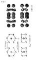
- Fig. 1 shows a structure of a WSi 10 film. As shown in an enlarged view of Fig. 1 , the WSi 10 film has a structure in which a W-Si-Si-W network is formed. The structure makes it possible to form a semiconductor thin film having the foregoing function.
- Fig. 17 shows the bonding between silicon atoms so as to highlight ten Si atoms around a W atom.
- An upper right diagram of Fig. 1 shows an enlarged view of a portion that is surrounded by a line of a left diagram of Fig. 1
- a lower right diagram of Fig. 1 shows a WSi 10 cluster used as a unit structure.
- the MSi n film widens a band gap thereof, and causes the MSi n film to have high resistance. Furthermore, because the MSi n film has a silicon cluster that contains M as a unit structure, a dangling bond of the silicon atoms is ended at the M that is disposed inside the silicon atoms. Therefore, the MSi n film does not require a hydrogenation of dangling bond in order to form a finite band gap though amorphous silicon requires it. As a result, the MSi n film is not so deteriorated in its function by dehydrogenation.
- a thin film in which MSi n is deposited is macroscopically amorphous.
- the thin film has a structure locally uniformed by having MSi n ("n" is a number ranging from 7 to 16) as a unit structure.
- MSi n is a number ranging from 7 to 16
- properties of a cluster that is a unit structure promise that an electronic state of the thin film is semiconducting, and the MSi n film is characteristic of having carrier mobility higher than that of amorphous silicon.
- MoSi 9 and MoSi 12 films are p-type and have 6.9 cm 2 /Vsec and 32.4 cm 2 /Vsec of mobility, respectively.
- a film in which a silicon cluster that contains M is a unit structure can be substituted for amorphous silicon in order to form a transistor of higher performance. It can be said that the film has mobility higher than that of a thin film of an organic semiconductor.
- Pentacene is known as an organic conductor material having high mobility.
- electron field-effect mobility of electron holes of p-type pentacene is no more than 0.75 cm 2 /Vsec.
- the thin film of the organic semiconductor is characteristic of being formed in low temperature and forming a transistor on various solid substrates.
- a MSi n film also can be deposited in room temperature, and can be formed on various solid substrates.
- a transition metal-containing silicon cluster is searched by first-principles calculation.
- a structure search by the first-principles calculation was conducted for a metal-silicon cluster having a composition in which a M atom has seven Si atoms.
- the transition metal M is titanium (Ti), vanadium (V), chromium (Cr), manganese (Mn), iron (Fe), cobalt (Co), nickel (Ni), zirconium (Zr), niobium (Nb), molybdenum (Mo), ruthenium (Ru), rhodium (Rh), hafnium (Hf), tantalum (Ta), tungsten (W), rhenium (Re), osmium (Os) or iridium (Ir), structures shown in Fig. 2 or other structures similar to those shown in Fig. 2 are stable, in which structures the M atom is surrounded by the silicon atoms.
- Fig. 2 shows a stable structure of MSi n ("n" ranges from 7 to 16), obtained by the first-principles calculation.
- M W.
- M Ti, V, Cr, Mn, Fe, Co, Ni, Cu, Zr, Nb, Mo, Ru, Rh, Pd, Ag, Hf, Ta, Re, Os, Ir, Pt or Au
- the MSi n has a structure similar to those shown in Fig. 2 .
- Gaussian03 was used for this calculation.
- Chemical models used for this calculation were B3LYP/LanL2DZ and B3PW91/LanL2DZ.
- Fig. 2 shows structures wherein M may be W.
- a gap E HL between HOMO and LUMO and a gap E SL between SUMO and LUMO of the cluster range from 0.71 eV to 2.99 eV.
- a semiconductor film can be formed by agglomerating a transition metal-containing silicon cluster in which E SL is wide and which has odd electrons.
- Fig. 3 shows a stable structure obtained by the first-principles calculation, and shows a molecular orbital representing bonding between NbSi 12 , in a case where two of NbSi 12 in which E SL is 1.06 eV are bonded to each other, that is, in a case where a dimmer is formed.
- the Nisi 12 stabilized when a distance between bonded silicon atoms that are closest to each other was 0.32 nm.
- gaps E HL of stable structures of other MSi 12 having odd electrons were determined as follows: E HL was 0.844 eV in a case of a TaSi 12 dimer; E HL was 0.381 eV in a case of a ReSi 12 dimer; E HL was 0.816 eV in a case of a VSi 12 dimer; and E HL was 0.354 eV in a case of a MnSi 12 dimer.
- gaps E HL of stable structures of dimers of MSi n having odd electrons and having a different silicon composition were determined as follows:, E HL was 2.50 eV in a case of NbSi 7 ; and E HL was 1.61 eV in a case of ReSi 10 . As a result, it was found that these stable structures have semiconducting properties.
- Fig. 4 shows a structure of a hydrogenated transition metal-containing silicon cluster (hereinafter referred to as "MSi n H x " in this specification, and note that "x" ranges from 2 to 12), figured by first-principles calculation. From Fig. 4 , it is apparent that, even if the transition metal-containing silicon cluster is hydrogenated, the transition metal-containing silicon cluster retains, by W-Si bonding, a structure in which a W atom is surrounded by Si atoms.
- MSi n H x hydrogenated transition metal-containing silicon cluster
- Fig. 5 shows a basic structure of a device.
- a reference sign 1 represents a transition metal target
- a reference sign 2 represents a sample substrate and a holder
- a reference sign 3 represents a vacuum chamber
- a reference sign 4 represents a gate valve
- a reference sign 5 represents a quartz cluster growing pipe
- a reference sign 6 represents a bypass line and a leak valve
- a reference sign 7 represents a Nd:YAG laser (wavelength: 532 nm, repetition frequency: 20 Hz, pulse width: 7 ns, and 1W)
- a reference sign 8 represents a multilayer mirror
- a reference 9 represents a plane-convex lens
- a reference sign 10 represents a vacuum gauge
- a reference sign 11 represents a variable leak valve
- a reference sign 12 represents a rotating motor.
- the process for producing the thin film of the metal-silicon compound is as described below.
- the process for producing the thin film of the metal-silicon compound on a surface of a solid substrate is as described below.
- the deposited MSi n H x is exposed to 0.1 Pa to 10 Pa of SiH 4 .
- a temperature on a surface of a sample substrate is controlled in the range from room temperature to 400 °C, and the deposited MSi n H x is reacted to the SiH 4 .
- the MSi n H x is annealed at 300 °C to 500 °C under ultra high vacuum, thereby dehydrogenating MSi n H x . This forms a MSi n film.
- the target used for laser ablation is a transition metal target.
- a compound target of metal atoms and silicon may be used. That is, from the compound target of the metal atoms and the silicon, the transition metal atoms and silicon atoms are emitted by laser ablation method, and thereby the transition metal-containing silicon cluster is synthesized.
- the transition metal atoms and the silicon atoms may be emitted into monosilane gas from the compound target of the transition metal atoms and the silicon by laser ablation method, so as to react the transition metal atoms with monosilane in the gas phase. This synthesizes a hydrogenated transition metal-containing silicon cluster.
- this process in which the compound target is used can achieve a higher deposition rate than the use of the transition metal target, and more saves monosilane gas than the use of the transition metal target because a film of high silicon content can be easily formed.
- the following describes a composition of a MSi n film and a result of structural analysis of the MSi n film, obtained by X-ray photoelectron spectroscopy.
- MoSi n and NbSi n films having various composition ratios "n" of Si to M are synthesized by adjusting pressure and flow rate of SiH 4 , and ablation conditions for M, such as laser intensity.
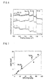
- Fig. 6 shows X-ray photoelectron spectroscopy (XPS) spectrum of MoSin.
- Fig. 6 shows XPS spectrum in a case where ablation was performed on Mo by 0.3 W of Nd:YAG pulse laser (wavelength: 532 nm, repetition frequency: 20 Hz, and pulse width: 7 ns), and where pressure of SiH4 atmosphere was 10 Pa, 15 Pa or 20 Pa.
- peaks of Mo 3p and Mo 3d and peaks of Si 2s and Si 2p were found.
- the peak intensity ratio of the Mo 3p to the Si 2p reflects a composition ratio of M to Si.
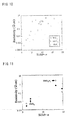
- Fig. 7 shows a plot of MoSin and NbSin film compositions in RBS spectrum against relative intensity of each peak of Si 2p and Mo 3p in XPS spectrum.
- the MoSi n and NbSi n films are substantially in proportion to each other.
- control of the pressure of SiH 4 atmosphere or the like enabled formation of the MoSi n and NbSi n films having different compositions.
- MSi n when "n" of MSi n is seven or more, MSi n has a structure in which a M atom is surrounded by Si atoms.
- a transition metal element has high reactivity with oxygen and water. Therefore, when the transition metal element is exposed to the air, the transition metal element is oxidized.
- M is surrounded by a network of Si, thereby suppressing oxidization of M.
- XPS spectrum of the MSi n film was measured after the MSi n film was exposed to the air.
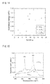
- Fig. 8 shows XPS spectrum of a NbSi 13 film before and after exposure to the air.
- a peak of O 1s was detected.
- peaks of Si 2p and Nb 3d were examined in detail ( Fig. 9 ).
- 104 eV of peak in which a signal of the Si 2p indicates formation of SiO 2 was detected after exposure to the air.
- the peak of the Nb 3d hardly changed before and after exposure to the air, and that Nb was not oxidized.
- the NbSi 13 film has a structure in which Nb is surrounded by a network of Si.
- Composition ratio "n" of Si to M was calculated by Rutherford backscattering spectrometry and X-ray photoelectron spectroscopy. The resistivity was obtained from a result of four-terminal electric conductivity measurement.
- Fig. 10 plots resistivity of each of the WSi n , MoSi n and NbSi n films against the composition ratio "n".
- the resistivity of the MoSi n exceeds 1 ⁇ cm in a region where n>5. This indicates that metal electric conductivity is shifted toward semiconducting conductivity as the number of "n" increases.
- the resistivity of the NbSi n film is substantially one or two digits lower than that of the MoSi n film even if the NbSi n film and the MoSi n film have an identical Si/M composition. This indicates that physicality of the MSi n film is controllable depending on types of a transition metal-containing unit structure cluster.
- Fig. 11 shows a change of resistivity before and after a deposited NbSi n H x is heated at 500 °C.
- the NbSi n H x is dehydrogenated by heat treatment. This causes a change of resistivity of the NbSi n H x .
- the NbSi n H x film becomes a semiconductor film along with an increase of the number of "n".
- pre-heat treatment is represented as a white circle
- after-heat treatment is represented as a black circle.
- the heat treatment dehydrogenates NbSi n H x , thereby forming a NbSi n film.
- the resistivity is obtained from a result of four-terminal electric conductivity measurement. Note that SiO 2 was used as a deposition substrate.
- the following describes a measurement result of an absorption edge of a MSi n film, obtained by light absorption spectrum measurement.
- the absorption edge of the MSi n film was measured in order to estimate a band gap of the MSi n film.
- Light absorption spectrum of the MSi n film was measured in the range from 240 nm to 2600 nm of wavelength, and fitting was performed by Tauc method, in order to obtain the absorption edge of the MSi n film.
- Fig. 12 shows composition dependency of an absorption edge of a MSi n film.
- Composition ratio "n" of Si to M was calculated by Rutherford backscattering spectrometry and X-ray photoelectron spectroscopy.
- n>5 a value of the absorption edge increased along with an increase of the number of "n”.
- This indicates that the MSi n becomes more semiconducting as the number of "n” increases, and that a band gap reaches substantially 1 eV around n 10.
- This change of the absorption edge clearly describes the composition dependency of the resistivity of the MSi n shown in Fig. 10 .
- Fig. 13 shows temperature dependency against conductivity of the MSi n film, that is, an Arrhenius plot.
- (a) represents a MoSi n film
- (b) represents a NbSi n film.
- the conductivity of the MSi n film increases along with an increase of temperature (T), and the MSi n film represents a semiconducting feature.
- the Arrhenius plot representing the conductivity against sample temperature T -1 is proportional to T -1 , and fitting is performed on the conductivity to obtain activation energy E a .
- Fig. 14 shows "n" dependency of activation energy of a MSi n film.
- Fig. 14 also shows that the activation energy E a of electric conductivity of the MSi n film is prone to increase along with an increase of the number of "n", and that the MSi n film takes on a semiconducting feature instead of a metal feature. It may be considered that, particularly, activation energy of a NbSi 5 is 0.01 eV that is greatly small, and that the NbSi 5 has a feature similar to that of metal. Meanwhile, a MoSi 12 film has 0.12 eV of activation energy, and has substantially at least 0.24 eV of a band gap as a semiconductor material.
- a thin film in which Mo was doped into amorphous silicon was formed, and electric conductivity feature of the thin film was compared to that of another film.
- An amorphous silicon film whose thickness is 150 nm was formed on a SiO 2 substrate by sputter deposition technique.
- Resistivity of such a formed Mo-doped amorphous silicon film was 0.24 ⁇ cm in room temperature. This is substantially one fiftieth lower than 13.4 ⁇ cm that is resistivity of a MoSi 12 film.
- Activation energy of electric conductivity of the Mo-doped amorphous silicon film is 0.048 eV. This is substantially 1/2.5 of the MoSi 12 film. That is, formation of a cluster film enables formation of a more semiconducting film.
- a carrier type and carrier density of each of MoSi n and NbSi n films Hall effect measurement was performed. Table 2 shows the results. Hall measurement results of the Mo-doped amorphous silicon film are also shown so as to compare to those of the MoSi n and NbSi n films.
- the carrier types of the films are different from each other depending on cluster compositions. In a case of Mo, when "n" was 8, 9 or 12, the carrier type of the MoSi n film was p-type, and when "n" was 16, the carrier type was n-type.
- the carrier types are controllable by changing types of M instead of changing a silicon composition.
- the carrier types of the NbSi n film are all n-type.
- the carrier density is also controllable in the range from 10 14 cm -3 to 10 20 cm -3 .
- the MoSi n and NbSi n films can be industrially substituted for the amorphous silicon film.
- the carrier density of the MoSi n or NbSi n film ranges from 10 14 to 10 18 , and the MoSi n film is semiconducting.
- the carrier density of the Mo-doped amorphous silicon film is 5.4 ⁇ 10 20 . Therefore, it can be considered that the Mo-doped amorphous silicon film represents a metal electronic state. This is a result that corresponds to estimation of the activation energy E a of the electric conductivity described above.
- Fig. 15 shows a result of Raman scattering measurement of a crystalline tungsten disilicide (c-WSi 2 ) and a WSi 14 film.
- a c-WSi 2 has Eg vibration of W-Si around 333 cm -1 and A 1g vibration of W-Si around 453 cm -1 but has no silicon optical phonon which a WSi 14 film has around 471 cm -1 .
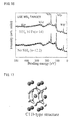
- Fig. 16 shows XPS spectrum of a MSi n film obtained by depositing a WSi 2 target at a substrate temperature of 280 °C and then annealing the MSi n film for 10 minutes at 500 °C under ultra high vacuum.
- Fig. 16 also shows two cases: a case where no SiH 4 is used and a case where 30 Pa of SiH 4 is used. From Fig.
Landscapes
- Chemical & Material Sciences (AREA)
- Organic Chemistry (AREA)
- Engineering & Computer Science (AREA)
- Materials Engineering (AREA)
- Mechanical Engineering (AREA)
- Metallurgy (AREA)
- Chemical Kinetics & Catalysis (AREA)
- General Chemical & Material Sciences (AREA)
- Inorganic Chemistry (AREA)
- Health & Medical Sciences (AREA)
- Toxicology (AREA)
- Physical Vapour Deposition (AREA)
- Electrodes Of Semiconductors (AREA)
- Insulated Gate Type Field-Effect Transistor (AREA)
Abstract
Description
- The present invention relates to a thin film of a metal-silicon compound used as a semiconductor thin film of a thin film transistor and the like, and a process for producing the thin film of the metal-silicon compound.
- Films made from crystalline silicon and amorphous silicon can be made with ultrathin thicknesses. Actually, it has been reported that a crystalline silicon layer can be formed with an average thickness of 0.7 nm by thermal oxidation of a SOI (Silicon on Insulator) substrate (see Non-Patent Literature 1). However, in such a thin film, it is difficult to control an interfacial structure thereof in an atomic layer level, whereby an interface state such as a defect or the like is caused in the thin film. Further, due to the ultrathin thickness of the ultrathin conducting layer, the interface state causes carrier scattering, thereby affecting conductivity in the ultrathin conducting layer. Actual mobility of electrons in the crystalline silicon having 0.7 nm in thickness is 50 cm2/Vsec. This is extremely inferior to 1000 cm2/Vsec or less that is mobility of bulk crystalline silicon. Furthermore, in such a thin film structure, conductive control by doping cannot be performed because a so-called dopant itself, such as phosphorus and boron, causes carrier scattering.
- Amorphous silicon is a semiconducting material used for a TFT of liquid crystal, a solar cell and the like. However, the amorphous silicon has lower mobility than crystalline silicon whose mobility is 1 cm2/Vsee for n-type semiconductor and the mobility of the crystalline silicon is 0.1 cm2/Vsec for p-type semiconductor. Therefore, the amorphous silicon cannot be used for a material for a high-performance device such as a LSI. Further, the amorphous silicon requires a hydrogenation of dangling bond so as to retain properties as a semiconducting material. However, it has been known that, because the end of the dangling bond is dehydrogenated by hot electron or photoirradiation, a device having the amorphous silicon falls into out of order.
- There has been known that organic materials, such as a pentacene, encompass a material having mobility higher than the amorphous silicon. The material has been regarded as a potential material for organic devices such as an electroluminescence, a field effect transistor and a solar cell (see Non-Patent Literature 2).
- However, electron field-effect mobility of electron holes of p-type pentacene is no more than 0.75 cm2/Vsec (see Non-Patent Literature 3). Therefore, the electron field-effect mobility of the electron holes of the p-type pentacene is inferior to the mobility of the crystalline silicon. As a result, the p-type pentacene cannot be a material for the high-performance device. Further, the p-type pentacene has lower heat resistance and oxidation resistance than those of silicon materials. The p-type pentacene is also inferior in stable performance. Particularly, the p-type pentacene has a melting point of substantially 300 °C, and therefore, cannot be used for a device that would reach a high temperature.
- A patent (see Patent Literature 1) discloses a cluster compound of a transition metal and silicon. However, the patent does not disclose an array of the cluster compound.
- Another patent (see Patent Literature 2) discloses that a semiconductor is made of a laminated substance in which a transition metal-containing silicon cluster having a MSi12 composition is arranged. This patent also discloses a semiconductor device that uses the laminated substance. However, the semiconductor device is not sufficiently functional because the laminated substance has a narrow band gap.
- Paten Literature 1
Japanese Patent Application Publication, Tokukai, No.2000-327319 A -
Patent Literature 2
Japanese Patent Application Publication, Tokukai, No.2008-28125 A - Non-Patent
Literature 1
IEEE International Electron Devices Meeting 2003 Technical Digest, p805 - Non-Patent
Literature 2
Journal of the Physical Society of Japan 2007, vol. Nov., p851 - Non-Patent Literature 3
Advanced Materials 2007, viol.19, p678 - An object of the present invention is to provide a thin film of a metal-silicon compound in which a gap EHL between highest occupied molecular orbital (HOMO) and lowest unoccupied molecular orbital (LUMO) is wide, and to provide a process for producing the thin film of the metal-silicon compound.
- In order to attain the foregoing object, the present invention provides the followings.
- (1) A thin film of a metal-silicon compound, the metal-silicon compound being a compound of a transition metal and silicon, in which compound a unit structure is a transition metal-containing silicon cluster, the transition metal-containing silicon cluster having a structure in which a transition metal atom is surrounded by seven to sixteen silicon atoms, two of which are first and second neighbor atoms to the transition metal atom.
- (2) The thin film of the metal-silicon compound as set forth in (1) wherein: the transition metal atom is any one of titanium, vanadium, chromium, manganese, iron, cobalt, nickel, zirconium, niobium, molybdenum, ruthenium, rhodium, hafnium, tantalum, tungsten, rhenium, osmium and iridium.
- (3) The thin film of the metal-silicon compound as set forth in (2) wherein: the transition metal atom is molybdenum or tungsten, and the number of silicon atoms is ten or twelve in the unit structure.
- (4) A thin film of a hydrogenated metal-silicon compound, being made by hydrogenating a transition metal-containing silicon cluster as set forth in (1) or (2).
- (5) A process for producing a thin film of a metal-silicon compound as set forth in any one of (1) to (3), comprising the steps of: synthesizing in advance a transition metal-containing silicon cluster in which the transition metal atom is surrounded by four to sixteen silicon atoms; and agglomerating the synthesized transition metal-containing silicon cluster.
- (6) A process for producing a thin film of a metal-silicon compound as set forth in any one of (1) to (3), comprising the step of: emitting the transition metal atom into monosilane gas by laser ablation method, so as to synthesize the transition metal-containing silicon cluster by gas phase reaction of the transition metal atom with monosilane.
- (7) A process for producing a thin film of a metal-silicon compound as set forth in any one of (1) to (3), comprising the step of: emitting the transition metal atom and a silicon atom from a compound target of the transition metal atom and silicon by laser ablation method, so as to synthesize the transition metal-containing silicon cluster.
- (8) A process for producing a thin film of a metal-silicon compound as set forth in any one of (1) to (3), comprising the steps of: depositing the transition metal-containing silicon cluster on a surface of a solid substrate; and reacting the deposited transition metal-containing silicon cluster with monosilane, so as to form a structure in which the transition metal atom is surrounded by seven to sixteen silicon atoms.
- (9) A process for producing a thin film of a hydrogenated metal-silicon compound as set forth in (4), comprising the steps of: synthesizing in advance a hydrogenated transition metal-containing silicon cluster in which the transition metal atom is surrounded by four to sixteen silicon atoms; and agglomerating the synthesized hydrogenated transition metal-containing silicon cluster.
- (10) A process for producing a thin film of a hydrogenated metal-silicon compound as set forth in (4), comprising the step of: emitting the transition metal atom into monosilane gas by laser ablation method, so as to synthesize the hydrogenated transition metal-containing silicon cluster by gas phase reaction of the transition metal atom with monosilane.
- (11) A process for producing a thin film of a hydrogenated metal-silicon compound as set forth in (4), comprising the step of: emitting the transition metal atom and a silicon atom into monosilane gas from a compound target of the transition metal atom and silicon by laser ablation method, so as to synthesize the hydrogenated transition metal-containing silicon cluster by gas phase reaction of the transition metal atom with monosilane.
- (12) A process for producing a thin film of a hydrogenated metal-silicon compound as set forth in (4), comprising the steps of: depositing the hydrogenated transition metal-containing silicon cluster on a surface of a solid substrate; and reacting the deposited hydrogenated transition metal-containing silicon cluster with monosilane, so as to form a structure in which the transition metal atom is surrounded by seven to sixteen silicon atoms.
- The present invention makes it possible to produce a semiconductor film having a finite band gap by agglomerating a transition metal-containing silicon cluster because the transition metal-containing silicon cluster is a semiconductor in which a gap EHL between highest occupied molecular orbital (HOMO) and lowest unoccupied molecular orbital (LUMO) is wide.
- Particularly, in a case where a transition metal M is Mo or W, and in a case where a transition metal-containing silicon cluster in which the number of silicon atoms is ten or twelve is deposited, the band gap of the semiconductor film exceeds 0.8 eV that is a value necessary for an operation of a transistor in room temperature.
- When the number of valence electrons of a contained transition metal M is odd, the total number of valence electrons of a transition metal-containing silicon cluster becomes odd (odd electron). Therefore, strictly speaking, EHL becomes 0 eV. However, agglomeration of the transition metal-containing silicon cluster forms bonding between clusters. Further, interchange of an electric charge causes structural relaxation, thereby allowing formation of a semiconductor film, as in a case where the transition metal-containing silicon cluster having even electrons is agglomerated. That is, the semiconductor film is formed by agglomerating a transition metal-containing silicon cluster in which a gap ESL, instead of EHL, between semi-unoccupied molecular orbital (SUMO) and LUMO is wide.
-
-
Fig. 1
Fig. 1 shows a WSi10 film in which Wsi10 of the present invention is a unit structure. -
Fig. 2
Fig. 2 shows a stable structure of MSin ("n" is a number in a range of 7 to 16), obtained by first-principles calculation. -
Fig. 3
Fig. 3 shows a stable structure of a NbSi12 dimer, obtained by first-principles calculation, and shows a molecular orbital representing existence of bonding between NbSi12. -
Fig. 4
Fig. 4 shows a change of a stable structure, caused by hydrogenating WSi12 into WSi12Hx. -
Fig. 5
Fig. 5 is a plan view of MSin cluster deposition system. -
Fig. 6
Fig. 6 shows XPS spectrum of a MoSin film. -
Fig. 7
Fig. 7 shows a plot of MoSin and NbSin film compositions in RBS spectrum against relative intensity of each ofSi 2p peak andMo 3p peak in the XPS spectrum. -
Fig. 8
Fig. 8 shows XPS spectrum of a NbSi13 film before and after exposure to the air. -
Fig. 9
Fig. 9 shows detailed spectrum around Si2p and Nb3d in XPS spectrum of a NbSi13 film before and after exposure to the air. -
Fig. 10
Fig. 10 shows a change of resistivity of each of WSin, MoSin and NbSin films, plotted against Si/M=n. -
Fig. 11
Fig. 11 shows a change of resistivity plotted against "n" before and after a NbSinHx film is heated at 500 °C. -
Fig. 12
Fig. 12 shows a change of absorption edges of WSin, MoSin and NbSin films, plotted against Si/M=n. -
Fig. 13
Fig. 13 shows Arrhenius plots indicative of temperature dependence of resistivity of a MSin film. -
Fig. 14
Fig. 14 shows "n" dependence of activation energy of a MSin (M is Mo, Nb or W) film. -
Fig. 15
Fig. 15 shows a result of Raman scattering measurement of a crystalline tungsten disilicide (c-WSi2) and a WSi14 film. -
Fig. 16
Fig. 16 shows XPS spectrum of a WSin film obtained by depositing a WSi2 target at a substrate temperature of 280 °C and then annealing the WSin film for 10 minutes at 500 °C under ultra high vacuum. -
Fig. 17
Fig. 17 shows a C11b type crystalline structure of WSi2. - The following schematically describes a thin film of a metal-silicon compound of the present invention.
- No silicon cluster that contains a transition metal exists in a metal silicide MSi2. For example, in a MSi2 crystalline structure (C11b type) as shown in
Fig. 17 , ten Si atoms are disposed around a W atom, and further other W atoms are disposed around the ten Si atoms. That is, in the MSi2 crystalline structure, ten Si atoms are shared by a plurality of W atoms, Si atoms are first neighbor atoms to the W atom, and the other W atoms are second neighbor atoms to the W atom. - On the contrary, the thin film of the metal-silicon compound (hereinafter referred to as a "MSin film" in this specification) of the present invention is characterized in that silicon atoms in a transition metal-containing silicon cluster (hereinafter referred to as "MSin" in this specification) is bonded to silicon atoms in another transition metal-containing silicon cluster, thereby causing silicon atoms to become second neighbor atoms to a transition metal M (hereinafter referred to as "M" in this specification).
Fig. 1 shows a structure of a WSi10 film. As shown in an enlarged view ofFig. 1 , the WSi10 film has a structure in which a W-Si-Si-W network is formed. The structure makes it possible to form a semiconductor thin film having the foregoing function. -
Fig. 17 shows the bonding between silicon atoms so as to highlight ten Si atoms around a W atom. An upper right diagram ofFig. 1 shows an enlarged view of a portion that is surrounded by a line of a left diagram ofFig. 1 , and a lower right diagram ofFig. 1 shows a WSi10 cluster used as a unit structure. - Further, hydrogenation of the MSin film widens a band gap thereof, and causes the MSin film to have high resistance. Furthermore, because the MSin film has a silicon cluster that contains M as a unit structure, a dangling bond of the silicon atoms is ended at the M that is disposed inside the silicon atoms. Therefore, the MSin film does not require a hydrogenation of dangling bond in order to form a finite band gap though amorphous silicon requires it. As a result, the MSin film is not so deteriorated in its function by dehydrogenation.
- A thin film in which MSin is deposited is macroscopically amorphous. However, the thin film has a structure locally uniformed by having MSin ("n" is a number ranging from 7 to 16) as a unit structure. Further, properties of a cluster that is a unit structure promise that an electronic state of the thin film is semiconducting, and the MSin film is characteristic of having carrier mobility higher than that of amorphous silicon. Actually, MoSi9 and MoSi12 films are p-type and have 6.9 cm2/Vsec and 32.4 cm2/Vsec of mobility, respectively. Accordingly, a film in which a silicon cluster that contains M is a unit structure can be substituted for amorphous silicon in order to form a transistor of higher performance. It can be said that the film has mobility higher than that of a thin film of an organic semiconductor. Pentacene is known as an organic conductor material having high mobility. However, electron field-effect mobility of electron holes of p-type pentacene is no more than 0.75 cm2/Vsec. The thin film of the organic semiconductor is characteristic of being formed in low temperature and forming a transistor on various solid substrates. A MSin film also can be deposited in room temperature, and can be formed on various solid substrates.
- The following describes, in detail, the thin film of the metal-silicon compound of the present invention and a process for producing the thin film of the meta-silicon compound, with reference to drawings.
- First, a transition metal-containing silicon cluster is searched by first-principles calculation.
- A structure search by the first-principles calculation was conducted for a metal-silicon cluster having a composition in which a M atom has seven Si atoms. As a result, it was found that, when the transition metal M is titanium (Ti), vanadium (V), chromium (Cr), manganese (Mn), iron (Fe), cobalt (Co), nickel (Ni), zirconium (Zr), niobium (Nb), molybdenum (Mo), ruthenium (Ru), rhodium (Rh), hafnium (Hf), tantalum (Ta), tungsten (W), rhenium (Re), osmium (Os) or iridium (Ir), structures shown in
Fig. 2 or other structures similar to those shown inFig. 2 are stable, in which structures the M atom is surrounded by the silicon atoms. -
Fig. 2 shows a stable structure of MSin ("n" ranges from 7 to 16), obtained by the first-principles calculation. InFig. 2 , M = W. Even in a case where the M is Ti, V, Cr, Mn, Fe, Co, Ni, Cu, Zr, Nb, Mo, Ru, Rh, Pd, Ag, Hf, Ta, Re, Os, Ir, Pt or Au, the MSin has a structure similar to those shown inFig. 2 . Gaussian03 was used for this calculation. Chemical models used for this calculation were B3LYP/LanL2DZ and B3PW91/LanL2DZ. -
Fig. 2 shows structures wherein M may be W. As shown in Table 1, a gap EHL between HOMO and LUMO and a gap ESL between SUMO and LUMO of the cluster range from 0.71 eV to 2.99 eV. - The following describes that a semiconductor film can be formed by agglomerating a transition metal-containing silicon cluster in which ESL is wide and which has odd electrons.
Fig. 3 shows a stable structure obtained by the first-principles calculation, and shows a molecular orbital representing bonding between NbSi12, in a case where two of NbSi12 in which ESL is 1.06 eV are bonded to each other, that is, in a case where a dimmer is formed. The Nisi12 stabilized when a distance between bonded silicon atoms that are closest to each other was 0.32 nm. When a molecular orbital whose level is 1.85 eV lower than energy of HOMO having even electrons made of a Nisi12 dimer, is observed, it is apparent that the NbSi12 molecules show an amplitude due to bonding, thereby proving that bonding between clusters is formed in the NbSi12 molecules. The bond formation between the NbSi12 molecules is associated with charge transfer, thereby causing structural relaxation in which a distance between bonded silicon atoms of a part of six-membered Si ring of NbSi12 increases. In the structural relaxation, the electrons made of the NbSi12 dimer have a gap EHL that is 0.844 eV and semiconducting properties. Similarly, gaps EHL of stable structures of other MSi12 having odd electrons were determined as follows: EHL was 0.844 eV in a case of a TaSi12 dimer; EHL was 0.381 eV in a case of a ReSi12 dimer; EHL was 0.816 eV in a case of a VSi12 dimer; and EHL was 0.354 eV in a case of a MnSi12 dimer. Further, gaps EHL of stable structures of dimers of MSin having odd electrons and having a different silicon composition were determined as follows:, EHL was 2.50 eV in a case of NbSi7; and EHL was 1.61 eV in a case of ReSi10. As a result, it was found that these stable structures have semiconducting properties. -
Fig. 4 shows a structure of a hydrogenated transition metal-containing silicon cluster (hereinafter referred to as "MSinHx" in this specification, and note that "x" ranges from 2 to 12), figured by first-principles calculation. FromFig. 4 , it is apparent that, even if the transition metal-containing silicon cluster is hydrogenated, the transition metal-containing silicon cluster retains, by W-Si bonding, a structure in which a W atom is surrounded by Si atoms. This proves that, as long as the M-Si bonding is retained, the hydrogenation of MSin ("n" ranges from 7 to 16) having a silicon cluster structure, even if it occurs, will not deprive a transition metal-containing silicon cluster of the structure in which a M atom is surrounded by Si atoms. Based on this, it can be deduced that the number "x" of hydrogen atoms that can bond to MSin ranges from 1 to "n".[Table 1] TiSi n CoSi n NiSi n MoSi n HfSi n ReSi n n E HL (eV) n E SL (eV) n E HL (eV) n E HL (eV) n E HL (eV) n E SL (eV) 7 1.85 7 2.94 7 2.88 7 2.50 7 1.96 7 1.99 8 1.90 8 1.50 8 1.58 8 2.56 8 1.90 8 1.44 9 1.42 9 2.37 9 1.93 9 2.80 9 1.88 9 1.39 10 1.50 10 1.17 10 1.03 10 1.61 10 1.42 10 1.25 11 1.66 11 1.20 11 1.42 11 2.26 11 1.63 11 1.33 12 1.71 12 1.80 12 1.09 12 2.20 12 1.74 12 2.99 13 1.80. 13 1.39 13 1.25 13 2.48 13 1.66 13 1.22 14 0.90 14 1.69 14 1.63 14 1.58 14 0.82 14 1.01 15 1.50 15 1.55 15 1.58 15 1.50 15 1.33 15 1.20 16 2.12 16 1.03 16 1.88 16 1.74 16 2.12 16 1.28 VSi n MnSi n ZrSi n RuSi n TaSi n OsSi n n E SL (eV) n E SL (eV) n E HL (eV) n E HL (eV) n E SL (eV) n E HL (eV) 7 1.93 7 1.74 7 1.93 7 1.69 7 1.66 7 1.69 8 1.88 8 1.17 8 1.88 8 1.58 8 1.55 8 1.85 9 1.93 9 1.90 9 1.25 9 1.88 9 1.63 9 2.12 10 1.50 10 1.58 10 1.42 10 1.63 10 1.36 10 1.63 11 1.44 11 1.55 11 1.66 11 1.96 11 1.39 11 1.99 12 1.01 12 2.99 12 1.69 12 2.80 12 1.06 12 2.53 13 1.96 13 1.74 13 1.80 13 1.85 13 1.44 13 1.88 14 1.12 14 1.44 14 0.90 14 0.93 14 1.06 14 0.90 15 1.50 15 1.25 15 1.50 15 1.44 15 1.59 15 1.44 16 1.69 16 1.22 16 2.12 16 0.95 16 1.58 16 1.03 CrSi n FeSi n NbSi n RhSi n WSi n IrSi n n E HL (eV) n E HL (eV) n E SL (eV) n E SL (eV) n E HL (eV) n E SL (eV) 7 2.34 7 1.71 7 1.66 7 1.47 7 2.34 7 1.58 8 2.67 8 2.26 8 1.55 8 1.39 8 2.75 8 1.39 9 2.67 9 1.71 9 1.61 9 1.39 9 2.12 9 1.33 10 1.63 10 1.39 10 1.36 10 1.25 10 1.50 10 1.28 11 2.23 11 1.90 11 1.39 11 1.42 11 2.23 11 1.33 12 2.28 12 2.80 12 1.06 12 1.12 12 2.61 12 0.71 13 2.34 13 1.77 13 1.44 13 1.39 13 2.48 13 1.39 14 1.55 14 1.63 14 1.09 14 1.28 14 1.55 14 1.06 15 1.52 15 1.39 15 1.52 15 1.20 15 1.47 15 1.20 16 1.74 16 0.79 16 1.55 16 1.01 16 1.77 16 1.03 - The following describes, in detail, a process for producing a thin film of a metal-silicon compound of the present invention.
- Laser ablation is performed on a transition metal M in SiH4 atmosphere, thereby causing gas phase reaction of SiH4 with a M atom so as to form MSinHx. Then, the formed MSinHx is deposited on a surface of a solid substrate, thereby forming a film in which MSinHx and MSin clusters are agglomerated.
Fig. 5 shows a basic structure of a device. - In
Fig. 5 , areference sign 1 represents a transition metal target, areference sign 2 represents a sample substrate and a holder, a reference sign 3 represents a vacuum chamber, areference sign 4 represents a gate valve, areference sign 5 represents a quartz cluster growing pipe, areference sign 6 represents a bypass line and a leak valve, areference sign 7 represents a Nd:YAG laser (wavelength: 532 nm, repetition frequency: 20 Hz, pulse width: 7 ns, and 1W), areference sign 8 represents a multilayer mirror, areference 9 represents a plane-convex lens, areference sign 10 represents a vacuum gauge, areference sign 11 represents a variable leak valve, and areference sign 12 represents a rotating motor. - The process for producing the thin film of the metal-silicon compound is as described below.
- (1) A sample substrate is positioned in a holder, and a transition metal target is positioned in a rotating holder.
- (2) A vacuum chamber is vacuated substantially to 2.0 × 10⁻⁷ Pa by a turbo-molecular pump, and a gate valve is then closed. Then, the vacuuming is switched to connection to a bypass line.
- (3) 0.1 Pa to 30 Pa of SiH4 is introduced into the vacuum chamber through a leak valve.
- (4) The transition metal target is adjusted to be positioned at a focus of a plane-convex lens, and the transition metal target is irradiated by a Nd:YAG laser. Power of the Nd:YAG laser ranges from 0.25 W to 0.3 W, a pulse width of the laser is 7 ns, and repetition frequency of the pulse is 20 Hz. On the sample substrate that faces the transition metal target, MSinHx is deposited. The deposited film of MSinHx on the sample substrate is 10 × 10 mm2 in dimension and 10 nm to 40 nm in thickness.
- (5) The deposited film of MSinHx is annealed at 300 °C to 500 °C under ultra high vacuum, thereby dehydrogenating the MSinHx film. This forms a MSin film.
- The process for producing the thin film of the metal-silicon compound on a surface of a solid substrate is as described below.
- By performing (1) to (4) similar to those described above, MSinHx in which a transition metal atom M is surrounded by four to sixteen silicon atoms is deposited on the surface of the solid substrate.
- Thereafter,
(5) the deposited MSinHx is exposed to 0.1 Pa to 10 Pa of SiH4. At the time of exposure, a temperature on a surface of a sample substrate is controlled in the range from room temperature to 400 °C, and the deposited MSinHx is reacted to the SiH4. This forms a structure in which the transition metal atom M is surrounded by seven to sixteen silicon atoms.
(6) The MSinHx is annealed at 300 °C to 500 °C under ultra high vacuum, thereby dehydrogenating MSinHx. This forms a MSin film. - In the process for producing the thin film of the metal-silicon compound, the target used for laser ablation is a transition metal target. However, a compound target of metal atoms and silicon may be used. That is, from the compound target of the metal atoms and the silicon, the transition metal atoms and silicon atoms are emitted by laser ablation method, and thereby the transition metal-containing silicon cluster is synthesized.
- Similarly, the transition metal atoms and the silicon atoms may be emitted into monosilane gas from the compound target of the transition metal atoms and the silicon by laser ablation method, so as to react the transition metal atoms with monosilane in the gas phase. This synthesizes a hydrogenated transition metal-containing silicon cluster.
- As compared to the transition metal target, this process in which the compound target is used, especially in a case where the compound target is made of high-melting metal, can achieve a higher deposition rate than the use of the transition metal target, and more saves monosilane gas than the use of the transition metal target because a film of high silicon content can be easily formed.
- The following describes a composition of a MSin film and a result of structural analysis of the MSin film, obtained by X-ray photoelectron spectroscopy.
- MoSin and NbSin films having various composition ratios "n" of Si to M are synthesized by adjusting pressure and flow rate of SiH4, and ablation conditions for M, such as laser intensity.
-
Fig. 6 shows X-ray photoelectron spectroscopy (XPS) spectrum of MoSin. Concretely,Fig. 6 shows XPS spectrum in a case where ablation was performed on Mo by 0.3 W of Nd:YAG pulse laser (wavelength: 532 nm, repetition frequency: 20 Hz, and pulse width: 7 ns), and where pressure of SiH4 atmosphere was 10 Pa, 15 Pa or 20 Pa. InFig. 6 , peaks ofMo 3p andMo 3d and peaks of Si 2s andSi 2p were found. The peak intensity ratio of theMo 3p to theSi 2p reflects a composition ratio of M to Si. -
Fig. 7 shows a plot of MoSin and NbSin film compositions in RBS spectrum against relative intensity of each peak ofSi 2p andMo 3p in XPS spectrum. Actually, as shown inFig. 7 , in the plot of ratio of Si to M calculated from Rutherford backscattering spectrometry (RBS) spectrum against ratio of Si to M calculated from XPS of the MoSin and NbSin films, the MoSin and NbSin films are substantially in proportion to each other. As a result, it is apparent that control of the pressure of SiH4 atmosphere or the like enabled formation of the MoSin and NbSin films having different compositions. - As described above, when "n" of MSin is seven or more, MSin has a structure in which a M atom is surrounded by Si atoms. Generally, a transition metal element has high reactivity with oxygen and water. Therefore, when the transition metal element is exposed to the air, the transition metal element is oxidized. However, in a material in which a cluster is a unit structure, M is surrounded by a network of Si, thereby suppressing oxidization of M. In order to confirm that the MSin film has the structure in which M is surrounded by the network of Si, XPS spectrum of the MSin film was measured after the MSin film was exposed to the air.
-
Fig. 8 shows XPS spectrum of a NbSi13 film before and after exposure to the air. As a result of the exposure of the NbSi13 film to the air, a peak of O 1s was detected. At the time of detection, peaks ofSi 2p andNb 3d were examined in detail (Fig. 9 ). In the examination, 104 eV of peak in which a signal of theSi 2p indicates formation of SiO2 was detected after exposure to the air. Meanwhile, it was found that the peak of theNb 3d hardly changed before and after exposure to the air, and that Nb was not oxidized. As a result, it was found that the NbSi13 film has a structure in which Nb is surrounded by a network of Si. - The following describes a measurement result of resistivity of a MSin film.
-
Fig. 10 shows a change of resistivity of each of WSin, MoSin and NbSin films, plotted against Si/M=n. Composition ratio "n" of Si to M was calculated by Rutherford backscattering spectrometry and X-ray photoelectron spectroscopy. The resistivity was obtained from a result of four-terminal electric conductivity measurement. -
Fig. 10 plots resistivity of each of the WSin, MoSin and NbSin films against the composition ratio "n". As n=Si/M increases, the resistivity grows exponentially. Particularly, the resistivity of the MoSin exceeds 1 Ω cm in a region where n>5. This indicates that metal electric conductivity is shifted toward semiconducting conductivity as the number of "n" increases. Further, when the NbSin film is compared to the MoSin film, the resistivity of the NbSin film is substantially one or two digits lower than that of the MoSin film even if the NbSin film and the MoSin film have an identical Si/M composition. This indicates that physicality of the MSin film is controllable depending on types of a transition metal-containing unit structure cluster. -
Fig. 11 shows a change of resistivity before and after a deposited NbSinHx is heated at 500 °C. The NbSinHx is dehydrogenated by heat treatment. This causes a change of resistivity of the NbSinHx. However, the NbSinHx film becomes a semiconductor film along with an increase of the number of "n". - In
Fig. 11 , pre-heat treatment is represented as a white circle, and after-heat treatment is represented as a black circle. The heat treatment dehydrogenates NbSinHx, thereby forming a NbSin film. The resistivity is obtained from a result of four-terminal electric conductivity measurement. Note that SiO2 was used as a deposition substrate. - The following describes a measurement result of an absorption edge of a MSin film, obtained by light absorption spectrum measurement.
- The absorption edge of the MSin film was measured in order to estimate a band gap of the MSin film. Light absorption spectrum of the MSin film was measured in the range from 240 nm to 2600 nm of wavelength, and fitting was performed by Tauc method, in order to obtain the absorption edge of the MSin film.
-
Fig. 12 shows composition dependency of an absorption edge of a MSin film. Composition ratio "n" of Si to M was calculated by Rutherford backscattering spectrometry and X-ray photoelectron spectroscopy. In a case where n>5, a value of the absorption edge increased along with an increase of the number of "n". Around n=10, the absorption edge became substantially 1 eV. This indicates that the MSin becomes more semiconducting as the number of "n" increases, and that a band gap reaches substantially 1 eV around n=10. This change of the absorption edge clearly describes the composition dependency of the resistivity of the MSin shown inFig. 10 . - The following describes temperature dependency and activation energy of electric conductivity.
- In order to confirm that the MSin film has semiconducting conductive mechanism, temperature dependency of electric conductivity of the MSin film was examined.
-
Fig. 13 shows temperature dependency against conductivity of the MSin film, that is, an Arrhenius plot. InFig. 13, (a) represents a MoSin film, and (b) represents a NbSin film. - As shown in
Fig. 13 , the conductivity of the MSin film increases along with an increase of temperature (T), and the MSin film represents a semiconducting feature. The Arrhenius plot representing the conductivity against sample temperature T-1 is proportional to T-1, and fitting is performed on the conductivity to obtain activation energy Ea. -
Fig. 14 shows "n" dependency of activation energy of a MSin film.Fig. 14 also shows that the activation energy Ea of electric conductivity of the MSin film is prone to increase along with an increase of the number of "n", and that the MSin film takes on a semiconducting feature instead of a metal feature. It may be considered that, particularly, activation energy of a NbSi5 is 0.01 eV that is greatly small, and that the NbSi5 has a feature similar to that of metal. Meanwhile, a MoSi12 film has 0.12 eV of activation energy, and has substantially at least 0.24 eV of a band gap as a semiconductor material. - In order to show superiority in formation of a film in which MSin is a unit, a thin film in which Mo was doped into amorphous silicon was formed, and electric conductivity feature of the thin film was compared to that of another film. An amorphous silicon film whose thickness is 150 nm was formed on a SiO2 substrate by sputter deposition technique. In order to form the amorphous silicon film, a composition in which a ratio of Mo: Si = 1: 12 was used as a sputtered target. This allowed formation of an amorphous film in which Si/Mo=12. After deposition of the amorphous film, the deposited amorphous film was heated at 500 °C under ultra high vacuum as with the MSin film. Resistivity of such a formed Mo-doped amorphous silicon film was 0.24 Ω cm in room temperature. This is substantially one fiftieth lower than 13.4 Ω cm that is resistivity of a MoSi12 film. Activation energy of electric conductivity of the Mo-doped amorphous silicon film is 0.048 eV. This is substantially 1/2.5 of the MoSi12 film. That is, formation of a cluster film enables formation of a more semiconducting film.
- In order to estimate mobility, a carrier type and carrier density of each of MoSin and NbSin films, Hall effect measurement was performed. Table 2 shows the results. Hall measurement results of the Mo-doped amorphous silicon film are also shown so as to compare to those of the MoSin and NbSin films. The carrier types of the films are different from each other depending on cluster compositions. In a case of Mo, when "n" was 8, 9 or 12, the carrier type of the MoSin film was p-type, and when "n" was 16, the carrier type was n-type. The carrier types are controllable by changing types of M instead of changing a silicon composition. In a case where Nb is used, the carrier types of the NbSin film are all n-type. The carrier density is also controllable in the range from 1014 cm-3 to 1020 cm-3. These results indicate that changing a deposited cluster makes it possible to determine the carrier type and the carrier density as appropriate. Further, mobility of the MoSin film is substantially two to three digits greater than that of the Mo-doped amorphous silicon film. The mobility of the MoSin film is greater than that of general amorphous silicon. The NbSin film also has higher mobility than that of n-type amorphous silicon. Therefore, the MoSin and NbSin films can be industrially substituted for the amorphous silicon film. When carrier density of the MoSin or NbSin film is compared to that of the Mo-doped amorphous silicon film, the carrier density of the MoSin film ranges from 1014 to 1018, and the MoSin film is semiconducting. Meanwhile, the carrier density of the Mo-doped amorphous silicon film is 5.4 × 10²⁰. Therefore, it can be considered that the Mo-doped amorphous silicon film represents a metal electronic state. This is a result that corresponds to estimation of the activation energy Ea of the electric conductivity described above.
[Table 2] Samples carrier type mobility (cm2/Vs) carrier density (cm-3) Mosi8 p 13.1 1.3x10⁸ MoSi9 p 6.9 2.5x10¹⁸ MoSi12 p 32.4 1.5x10¹⁴ moSi16 n 2.8 1.4x10¹⁸ Mo-Si alloy (Si/Mo=12) n 0.05 5.4x10²⁰ NbSi7 n 9.88 9.9x10¹⁹ NbSi13 n 3.86 4.7x10¹⁸ NbSi15 n 0.68 1.5x10²⁰ - In order to describe structural features of a MSin film,
Fig. 15 shows a result of Raman scattering measurement of a crystalline tungsten disilicide (c-WSi2) and a WSi14 film. - A c-WSi2 has Eg vibration of W-Si around 333 cm-1 and A1g vibration of W-Si around 453 cm-1 but has no silicon optical phonon which a WSi14 film has around 471 cm-1. This proves that the WSi14 film has a silicon network which the c-WSi2 does not have and which is similar to an a-Si:H film formed therein.
- The following describes a result of composition analysis of a MSin film, obtained by X-ray photoelectron spectroscopy. The MSin film was made of a compound target of a transition metal atom and silicon.
Fig. 16 shows XPS spectrum of a MSin film obtained by depositing a WSi2 target at a substrate temperature of 280 °C and then annealing the MSin film for 10 minutes at 500 °C under ultra high vacuum.Fig. 16 also shows two cases: a case where no SiH4 is used and a case where 30 Pa of SiH4 is used. FromFig. 16 , it is apparent that signals of W 4p, W 4d and W 4f, and signals ofSi 2p and Si 2s were formed, and that a W-Si compound was formed. A Si/W composition "n" is estimated from peak intensity ratio of Si 2p3/2 to W 4f7/2: n = 12.2 in the case where no SiH4 was used; and n = 14 in the case where 30 Pa of SiH4 was used.
Claims (12)
- A thin film of a metal-silicon compound,
the metal-silicon compound being a compound of a transition metal and silicon, in which compound a unit structure is a transition metal-containing silicon cluster;
the transition metal-containing silicon cluster having a structure in which a transition metal atom is surrounded by seven to sixteen silicon atoms, two of which are first and second neighbor atoms to the transition metal atom. - The thin film of the metal-silicon compound as set forth in claim 1 wherein:
the transition metal atom is any one of titanium, vanadium, chromium, manganese, iron, cobalt, nickel, zirconium, niobium, molybdenum, ruthenium, rhodium, hafnium, tantalum, tungsten, rhenium, osmium and iridium. - The thin film of the metal-silicon compound as set forth in claim 2 wherein:
the transition metal atom is molybdenum or tungsten, and the number of silicon atoms is ten or twelve in the unit structure. - A thin film of a hydrogenated metal-silicon compound, being made by hydrogenating a transition metal-containing silicon cluster as set forth in claim 1 or 2.
- A process for producing a thin film of a metal-silicon compound as set forth in any one of claims 1 to 3, comprising the steps of:
synthesizing in advance a transition metal-containing silicon cluster in which the transition metal atom is surrounded by four to sixteen silicon atoms; and
agglomerating the synthesized transition metal-containing silicon cluster. - A process for producing a thin film of a metal-silicon compound as set forth in any one of claims 1 to 3, comprising the step of:
emitting the transition metal atom into monosilane gas by laser ablation method, so as to synthesize the transition metal-containing silicon cluster by gas phase reaction of the transition metal atom with monosilane. - A process for producing a thin film of a metal-silicon compound as set forth in any one of claims 1 to 3, comprising the step of:
emitting the transition metal atom and a silicon atom from a compound target of the transition metal atom and silicon by laser ablation method, so as to synthesize the transition metal-containing silicon cluster. - A process for producing a thin film of a metal-silicon compound as set forth in any one of claims 1 to 3, comprising the steps of:
depositing the transition metal-containing silicon cluster on a surface of a solid substrate; and
reacting the deposited transition metal-containing silicon cluster with monosilane, so as to form a structure in which the transition metal atom is surrounded by seven to sixteen silicon atoms. - A process for producing a thin film of a hydrogenated metal-silicon compound as set forth in claim 4, comprising the steps of:
synthesizing in advance a hydrogenated transition metal-containing silicon cluster in which the transition metal atom is surrounded by four to sixteen silicon atoms; and
agglomerating the synthesized hydrogenated transition metal-containing silicon cluster. - A process for producing a thin film of a hydrogenated metal-silicon compound as set forth in claim 4, comprising the step of:
emitting the transition metal atom into monosilane gas by laser ablation method, so as to synthesize the hydrogenated transition metal-containing silicon cluster by gas phase reaction of the transition metal atom with monosilane. - A process for producing a thin film of a hydrogenated metal-silicon compound as set forth in claim 4, comprising the step of:
emitting the transition metal atom and a silicon atom into monosilane gas from a compound target of the transition metal atom and silicon by laser ablation method, so as to synthesize the hydrogenated transition metal-containing silicon cluster by gas phase reaction of the transition metal atom with monosilane. - A process for producing a thin film of a hydrogenated metal-silicon compound as set forth in claim 4, comprising the steps of:
depositing the hydrogenated transition metal-containing silicon cluster on a surface of a solid substrate; and
reacting the deposited hydrogenated transition metal-containing silicon cluster with monosilane, so as to form a structure in which the transition metal atom is surrounded by seven to sixteen silicon atoms.
Applications Claiming Priority (4)
| Application Number | Priority Date | Filing Date | Title |
|---|---|---|---|
| JP2008048520 | 2008-02-28 | ||
| JP2008230650 | 2008-09-09 | ||
| JP2009037261A JP5464570B2 (en) | 2008-02-28 | 2009-02-20 | Metallic silicon compound thin film and method for producing the same |
| PCT/JP2009/053422 WO2009107669A1 (en) | 2008-02-28 | 2009-02-25 | Thin film of metal silicon compound and process for producing the thin film of metal silicon compound |
Publications (2)
| Publication Number | Publication Date |
|---|---|
| EP2253589A1 true EP2253589A1 (en) | 2010-11-24 |
| EP2253589A4 EP2253589A4 (en) | 2012-11-28 |
Family
ID=41016056
Family Applications (1)
| Application Number | Title | Priority Date | Filing Date |
|---|---|---|---|
| EP09714676A Ceased EP2253589A4 (en) | 2008-02-28 | 2009-02-25 | THIN FILM OF METAL-SILICON COMPOUND AND METHOD FOR PRODUCING THE THIN FILM OF METAL-SILICON COMPOUND |
Country Status (6)
| Country | Link |
|---|---|
| US (1) | US8367030B2 (en) |
| EP (1) | EP2253589A4 (en) |
| JP (1) | JP5464570B2 (en) |
| KR (1) | KR101228883B1 (en) |
| CN (1) | CN101959795B (en) |
| WO (1) | WO2009107669A1 (en) |
Cited By (1)
| Publication number | Priority date | Publication date | Assignee | Title |
|---|---|---|---|---|
| WO2014019571A1 (en) * | 2012-07-18 | 2014-02-06 | 2H.System | Method for producing protective layers containing silicides and/or oxidized silicides on substrates |
Families Citing this family (5)
| Publication number | Priority date | Publication date | Assignee | Title |
|---|---|---|---|---|
| JP4660743B1 (en) * | 2009-08-21 | 2011-03-30 | 独立行政法人産業技術総合研究所 | Thin film transistor |
| RU2458181C2 (en) * | 2010-08-17 | 2012-08-10 | Государственное образовательное учреждение высшего профессионального образования Московский государственный институт радиотехники, электроники и автоматики (Технический университет) (МИРЭА) | Method for obtaining ferromagnetic film from silicide nanoclusters on surface of silicone substrate |
| JP6044907B2 (en) * | 2012-03-06 | 2016-12-14 | 国立研究開発法人産業技術総合研究所 | Semiconductor contact structure and method of forming the same |
| KR102383369B1 (en) | 2016-06-17 | 2022-04-05 | 고쿠리츠켄큐카이하츠호진 상교기쥬츠 소고켄큐쇼 | Compound film of tungsten and germanium and semiconductor device |
| JP6896305B2 (en) * | 2017-11-09 | 2021-06-30 | 国立研究開発法人産業技術総合研究所 | Semiconductor devices and their manufacturing methods |
Family Cites Families (6)
| Publication number | Priority date | Publication date | Assignee | Title |
|---|---|---|---|---|
| JPS58190815A (en) * | 1982-04-30 | 1983-11-07 | Futaba Corp | Amorphous film of silicide of transition element |
| JPH0280554A (en) * | 1988-09-14 | 1990-03-20 | Hitachi Ltd | Formation of film of metallic silicide of high melting point |
| JP2000178713A (en) * | 1998-12-09 | 2000-06-27 | Japan Science & Technology Corp | Method of forming β-FeSi2 thin film |
| JP2000327319A (en) * | 1999-05-11 | 2000-11-28 | Agency Of Ind Science & Technol | Cluster and its production |
| JP2001081563A (en) * | 1999-09-17 | 2001-03-27 | Japan Science & Technology Corp | Method for producing erbium-doped hydrogenated amorphous silicon thin film |
| JP4873466B2 (en) * | 2006-07-20 | 2012-02-08 | 独立行政法人産業技術総合研究所 | Layered material and semiconductor device using the same |
-
2009
- 2009-02-20 JP JP2009037261A patent/JP5464570B2/en not_active Expired - Fee Related
- 2009-02-25 EP EP09714676A patent/EP2253589A4/en not_active Ceased
- 2009-02-25 CN CN200980106376.8A patent/CN101959795B/en not_active Expired - Fee Related
- 2009-02-25 WO PCT/JP2009/053422 patent/WO2009107669A1/en not_active Ceased
- 2009-02-25 US US12/919,443 patent/US8367030B2/en not_active Expired - Fee Related
- 2009-02-25 KR KR1020107020222A patent/KR101228883B1/en not_active Expired - Fee Related
Cited By (1)
| Publication number | Priority date | Publication date | Assignee | Title |
|---|---|---|---|---|
| WO2014019571A1 (en) * | 2012-07-18 | 2014-02-06 | 2H.System | Method for producing protective layers containing silicides and/or oxidized silicides on substrates |
Also Published As
| Publication number | Publication date |
|---|---|
| CN101959795A (en) | 2011-01-26 |
| JP5464570B2 (en) | 2014-04-09 |
| EP2253589A4 (en) | 2012-11-28 |
| JP2010093221A (en) | 2010-04-22 |
| US20110002833A1 (en) | 2011-01-06 |
| KR20100121649A (en) | 2010-11-18 |
| CN101959795B (en) | 2014-06-18 |
| KR101228883B1 (en) | 2013-02-01 |
| US8367030B2 (en) | 2013-02-05 |
| WO2009107669A1 (en) | 2009-09-03 |
Similar Documents
| Publication | Publication Date | Title |
|---|---|---|
| US8367030B2 (en) | Thin film of metal-silicon compound and process for producing the thin film of the metal-silicon compound | |
| JP5247448B2 (en) | Conductive film forming method and thin film transistor manufacturing method | |
| KR20120120902A (en) | Metal silicide, metal germanide, methods for making the same and nickel thin film depositions | |
| US5306529A (en) | Process for forming an ohmic electrode on a diamond film involving heating in a vacuum atmosphere | |
| US20210074543A1 (en) | Method of forming transition metal dichalcogenidethin film and method of manufacturing electronic device including the same | |
| KR101610623B1 (en) | Fabrication and method of deposition p-type Tin oxide thin film and Method of fabricating transistor | |
| US8293643B2 (en) | Method and structure of forming silicide and diffusion barrier layer with direct deposited film on silicon | |
| KR101289611B1 (en) | Silicon device structure and sputtering target material used in forming the same | |
| JPS6318342B2 (en) | ||
| JP6503543B2 (en) | Transition metal silicide film, method and apparatus for manufacturing the same, and semiconductor device | |
| JP4576201B2 (en) | Method for preparing molybdenum trioxide layer | |
| WO2001084609A1 (en) | Method for low temperature formation of stable ohmic contacts to silicon carbide | |
| KR100679224B1 (en) | Semiconductor device and manufacturing method | |
| US7446042B2 (en) | Method for silicide formation on semiconductor devices | |
| WO2003012876A1 (en) | Gate electrodes and the formation thereof | |
| US20090035173A1 (en) | Electrically Conductive Material | |
| Wang et al. | Barrier capabilities of selective chemical vapor deposited W films and WSiN/WSi x/W stacked layers against Cu diffusion | |
| JP4660743B1 (en) | Thin film transistor | |
| KR100349625B1 (en) | Method for fabrication of epitaxial cobalt-disilicide layer at low temperatures | |
| CN101710577A (en) | Method for inhibiting oxidization of copper in copper interconnect structure | |
| KR100325302B1 (en) | Method for Manufacturing of Semiconductor Device | |
| JP5196505B2 (en) | Thin film transistor | |
| KR960007639B1 (en) | High purity conductive film for semiconductor device and semiconductor device using same | |
| KR101621852B1 (en) | Semiconductor device and method for manufacturing the same | |
| US20070120199A1 (en) | Low resistivity compound refractory metal silicides with high temperature stability |
Legal Events
| Date | Code | Title | Description |
|---|---|---|---|
| PUAI | Public reference made under article 153(3) epc to a published international application that has entered the european phase |
Free format text: ORIGINAL CODE: 0009012 |
|
| 17P | Request for examination filed |
Effective date: 20100903 |
|
| AK | Designated contracting states |
Kind code of ref document: A1 Designated state(s): AT BE BG CH CY CZ DE DK EE ES FI FR GB GR HR HU IE IS IT LI LT LU LV MC MK MT NL NO PL PT RO SE SI SK TR |
|
| AX | Request for extension of the european patent |
Extension state: AL BA RS |
|
| DAX | Request for extension of the european patent (deleted) | ||
| RIC1 | Information provided on ipc code assigned before grant |
Ipc: C23C 16/42 20060101ALI20121019BHEP Ipc: C23C 14/28 20060101ALI20121019BHEP Ipc: H01L 29/786 20060101ALI20121019BHEP Ipc: C01B 33/06 20060101AFI20121019BHEP |
|
| A4 | Supplementary search report drawn up and despatched |
Effective date: 20121029 |
|
| 17Q | First examination report despatched |
Effective date: 20140604 |
|
| APBK | Appeal reference recorded |
Free format text: ORIGINAL CODE: EPIDOSNREFNE |
|
| APBN | Date of receipt of notice of appeal recorded |
Free format text: ORIGINAL CODE: EPIDOSNNOA2E |
|
| APBR | Date of receipt of statement of grounds of appeal recorded |
Free format text: ORIGINAL CODE: EPIDOSNNOA3E |
|
| APAF | Appeal reference modified |
Free format text: ORIGINAL CODE: EPIDOSCREFNE |
|
| APBT | Appeal procedure closed |
Free format text: ORIGINAL CODE: EPIDOSNNOA9E |
|
| REG | Reference to a national code |
Ref country code: DE Ref legal event code: R003 |
|
| STAA | Information on the status of an ep patent application or granted ep patent |
Free format text: STATUS: THE APPLICATION HAS BEEN REFUSED |
|
| 18R | Application refused |
Effective date: 20200814 |