EP2251903A1 - Heat sink mounting method - Google Patents
Heat sink mounting method Download PDFInfo
- Publication number
- EP2251903A1 EP2251903A1 EP09305435A EP09305435A EP2251903A1 EP 2251903 A1 EP2251903 A1 EP 2251903A1 EP 09305435 A EP09305435 A EP 09305435A EP 09305435 A EP09305435 A EP 09305435A EP 2251903 A1 EP2251903 A1 EP 2251903A1
- Authority
- EP
- European Patent Office
- Prior art keywords
- circuit board
- printed circuit
- heat dissipating
- heat sink
- dissipating apparatus
- Prior art date
- Legal status (The legal status is an assumption and is not a legal conclusion. Google has not performed a legal analysis and makes no representation as to the accuracy of the status listed.)
- Granted
Links
Images


Classifications
-
- H—ELECTRICITY
- H10—SEMICONDUCTOR DEVICES; ELECTRIC SOLID-STATE DEVICES NOT OTHERWISE PROVIDED FOR
- H10W—GENERIC PACKAGES, INTERCONNECTIONS, CONNECTORS OR OTHER CONSTRUCTIONAL DETAILS OF DEVICES COVERED BY CLASS H10
- H10W40/00—Arrangements for thermal protection or thermal control
- H10W40/60—Securing means for detachable heating or cooling arrangements, e.g. clamps
-
- H—ELECTRICITY
- H05—ELECTRIC TECHNIQUES NOT OTHERWISE PROVIDED FOR
- H05K—PRINTED CIRCUITS; CASINGS OR CONSTRUCTIONAL DETAILS OF ELECTRIC APPARATUS; MANUFACTURE OF ASSEMBLAGES OF ELECTRICAL COMPONENTS
- H05K3/00—Apparatus or processes for manufacturing printed circuits
- H05K3/30—Assembling printed circuits with electric components, e.g. with resistors
- H05K3/303—Assembling printed circuits with electric components, e.g. with resistors with surface mounted components
- H05K3/305—Affixing by adhesive
-
- H—ELECTRICITY
- H10—SEMICONDUCTOR DEVICES; ELECTRIC SOLID-STATE DEVICES NOT OTHERWISE PROVIDED FOR
- H10W—GENERIC PACKAGES, INTERCONNECTIONS, CONNECTORS OR OTHER CONSTRUCTIONAL DETAILS OF DEVICES COVERED BY CLASS H10
- H10W95/00—Packaging processes not covered by the other groups of this subclass
-
- H—ELECTRICITY
- H05—ELECTRIC TECHNIQUES NOT OTHERWISE PROVIDED FOR
- H05K—PRINTED CIRCUITS; CASINGS OR CONSTRUCTIONAL DETAILS OF ELECTRIC APPARATUS; MANUFACTURE OF ASSEMBLAGES OF ELECTRICAL COMPONENTS
- H05K1/00—Printed circuits
- H05K1/02—Details
- H05K1/0201—Thermal arrangements, e.g. for cooling, heating or preventing overheating
- H05K1/0203—Cooling of mounted components
-
- H—ELECTRICITY
- H05—ELECTRIC TECHNIQUES NOT OTHERWISE PROVIDED FOR
- H05K—PRINTED CIRCUITS; CASINGS OR CONSTRUCTIONAL DETAILS OF ELECTRIC APPARATUS; MANUFACTURE OF ASSEMBLAGES OF ELECTRICAL COMPONENTS
- H05K2201/00—Indexing scheme relating to printed circuits covered by H05K1/00
- H05K2201/10—Details of components or other objects attached to or integrated in a printed circuit board
- H05K2201/10613—Details of electrical connections of non-printed components, e.g. special leads
- H05K2201/10621—Components characterised by their electrical contacts
- H05K2201/10734—Ball grid array [BGA]; Bump grid array
-
- Y—GENERAL TAGGING OF NEW TECHNOLOGICAL DEVELOPMENTS; GENERAL TAGGING OF CROSS-SECTIONAL TECHNOLOGIES SPANNING OVER SEVERAL SECTIONS OF THE IPC; TECHNICAL SUBJECTS COVERED BY FORMER USPC CROSS-REFERENCE ART COLLECTIONS [XRACs] AND DIGESTS
- Y02—TECHNOLOGIES OR APPLICATIONS FOR MITIGATION OR ADAPTATION AGAINST CLIMATE CHANGE
- Y02P—CLIMATE CHANGE MITIGATION TECHNOLOGIES IN THE PRODUCTION OR PROCESSING OF GOODS
- Y02P70/00—Climate change mitigation technologies in the production process for final industrial or consumer products
- Y02P70/50—Manufacturing or production processes characterised by the final manufactured product
Definitions
- This invention relates to mounting technology, especially to mounting a heat sink to a printed circuit board.
- a circuit board component e.g. an integrated circuit (IC) package which is for example soldered to a printed circuit board in Ball Grid Array (BGA) way (called BGA IC package hereafter)
- BGA IC package Ball Grid Array
- a heat sink is usually mounted on the surface of the circuit board component to dissipate the heat.
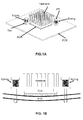
- Figs.1A, 1B , 1C and 1D show a conventional frequently used example which uses two arrow-ended pins to lock a heat sink attached on a BGA IC package to a PCB with a helical spring coiling around the pole of each pin between the head of the pin and the tab of the heat sink.
- Fig.1A is the isometric view.
- Fig.1B is a front view showing the case when the heat sink is statically mounted on the BGA IC package and further on the PCB. However, when the heat sink is mounted on the BGA IC package, it will further increase the weight on the PCB and this will generate a strain on the solder ball connections of Ball Grid Array (BGA) IC package.
- BGA Ball Grid Array
- Fig.1B From Fig.1B , it can be seen that the PCB is bended due to the increase of weight on top of the PCB.
- the whole assembled device/instrument heat sink, BGA package, and PCB
- the heat sink drops for example to the floor
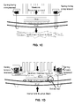
- the heat sink since the heat sink is locked to the PCB by the pins, due to the elasticity of the helical springs and the restraint of the arrow-ended pin, the heat sink will bounce up and down to hit the BGA IC package like a hammer, which may crack the solder balls of the BGA.
- Fig. 1C illustrates the situation when the helical spring is compressed due to the hit to for example the floor.
- Fig.1D shows the situation when the helical spring tension is released and the heat sink hammers the BGA IC package.
- a heat dissipating assembly which includes a printed circuit board; an electronic device, attached to the printed circuit board; a heat dissipating apparatus, bottom of which is attached to the surface of the electronic device and has at least a part exposed to the printed circuit board; and an adhesive element, disposed between the part of the bottom exposed to the printed circuit board and the printed circuit board to make the heat dissipating apparatus adhere to the printed circuit board.
- the heat dissipating apparatus comprises two tabs extending diametrically from the bottom and paralleling the printed circuit board when the bottom is of round shape, and two pins inserted through two tabs respectively to further lock the heat dissipating apparatus to the printed circuit board.
- the two tabs extend diagonally from the bottom and parallel the printed circuit board, when the bottom 21 is of rectangular shape.
- the at least one adhesive element is disposed between the two corners of the bottom of the heat dissipating apparatus without the tab of the heat dissipating apparatus to make the heat dissipating apparatus adhere to the printed circuit board.
- the at least one adhesive element is disposed at the four corners and the edges of the heat dissipating apparatus to make the heat dissipating apparatus adhere to the printed circuit board.
- adhesive element is epoxy glue and can't have chemical reaction with the PCB and the heat sink.
- the electronic device is a Ball Grid Array package, a Quad Flat No leads package, a Small Outline Package, or a Chip Support Package.
- a method for mounting a heat dissipating apparatus to a printed circuit board comprises steps of attaching an electronic device to the printed circuit board; mounting the heat dissipating apparatus on the electronic device, the bottom of the heat dissipating apparatus being attached to the surface of the electronic device and having at least a part exposed to the printed circuit board; and disposing adhesive between the part of the bottom exposed to the printed circuit board and the printed circuit board to make the heat dissipating apparatus adhere to the printed circuit board.
- step of disposing adhesive there is a step of locking the heat dissipating apparatus to the printed circuit board by using two pins through two tabs extending diagonal and paralleling the printed circuit board, a helical spring coiling the pole of each pin between the pin head and the printed circuit board.
- adhesive is epoxy glue.
- the electronic device is a Ball Grid Array package, a Quad Flat No leads package, a Small Outline Package, or a Chip Support Package.
- Fig. 2 shows a heat sink assembly mounted on a BGA IC package and further on a PCB according to an embodiment.
- the IC package 3 is fixed to a printed circuit board 1 in Ball Grid Array (BGA) way, and a heat sink 2 is mounted on the surface of the IC package 3 and further to the printed circuit board 1.
- BGA Ball Grid Array
- Two tabs 6 with apertures (not shown) thereon are extended paralleling the PCB 1 from two diagonal corners of the heat sink 2.
- two arrow-ended pins 4 with helical springs 5 coiled thereon and between the pin head and the tabs 6 are inserted to fasten the heat sink 2 to the PCB 1.
- an adhesive element e.g.
- glue 7 is used at the other two corners than the two corners with the tabs of the heat sink to further fasten it to the PCB.
- This glue is epoxy.
- the glue in Fig.2 is exaggeratedly drawn to illustrate the present principle, and should not be construed as limitation to the invention. By gluing the heat sink to the PCB, the glue will act as a stiffener to constrain the movement or flexing which prevents strain generated to the solder balls of the BGA.
- Fig. 3A is a top view of the heat sink 2 and the glue 7 in Fig.2 .
- the dashed lines in Fig.3A show the part of glue that spreads between the back of the heat sink 2 and the PCB 1 and can't be seen from the top.
- Fig. 3B is a bottom view of heat sink 2 with the glue 7, wherein sign 21 indicating the bottom surface of the heat sink.
- Fig.4 is a front view further showing how the glue is used in Fig.2, Fig.3A and Fig.3B .
- IC chip 31, substrate 32 and solder balls 33 constitute the BGA IC package 3.
- a part of the bottom surface of the heat sink 2 is exposed to the PCB 1. In Fig.4 , this part is the periphery of the bottom of the heat sink 2.
- the glue can be spotted between the two corners of the bottom surface of the heat sink 2 exposed to the PCB 1 and the PCB 1, or even stick the substrate 32, or further extend to the side face of IC chip 31 (not shown).
- Fig.5 is the isometric view of the variant embodiment.
- Fig. 6A is the top view of the heat sink 2 with glue 7 in Fig.5 . Dashed lines show invisible part of the glue at the back of the heat sink 2 and can't be seen from the top.
- Fig. 6B is the bottom view of the heat sink 2 with glue in Fig.5 .
- Fig.7 is the isometric view.
- Fig. 8A is the top view of the heat sink 2 with glue 7 in Fig.7 . Dashed lines show invisible part of the glue at the back of the heat sink 2 and can't be seen from the top.
- Fig. 8B is the bottom view of the heat sink 2 with glue in Fig.7 .
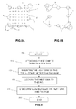
- Fig. 9 is a flow chart showing how to mount the heat sink assembly. As is seen from Fig.9 , the process starts at step 900 and ends at step 950. At step 910, the IC chip is attached to the PCB in BGA way. Then at step 920, the heat sink 2 is mounted on the surface of the BGA IC package 3. At step 930, two arrow-ended pins 4 are inserted in the two apertures of the two tabs 6 extending paralleling the PCB 1 from the bottom of the heat sink 2 to lock the heat sink 2 to the PCB.1. Afterwards, at step 940, glue 7 is disposed between the heat sink 2 and the PCB 1.
- the glue specified in above embodiments may be any type of epoxy glue which may not harm the PCB & BGA in any chemical reaction.
- the heat sink has a rectangular bottom.
- the present principle can be used too.
- two tabs can extend paralleling the PCB in from two diametric points of the heat sink bottom, and glue can be used at several points of periphery of a round shaped heat sink.
- the part of the bottom of the heat sink 2 that is exposed to the PCB 1 is the periphery of the bottom, it can be other parts, e.g. middle of the bottom of the heat sink. In the latter situation, there should be a corresponding part on the PCB so that the glue can be put between the two parts to force the heat sink adhere to the PCB.
- glue can be used to fasten a heat sink to a PCB without the pins or to fasten a heat sink in a different way, e.g. using a string spring. And these variants should be covered by the present principle.
Landscapes
- Engineering & Computer Science (AREA)
- Manufacturing & Machinery (AREA)
- Microelectronics & Electronic Packaging (AREA)
- Cooling Or The Like Of Semiconductors Or Solid State Devices (AREA)
Abstract
Description
- This invention relates to mounting technology, especially to mounting a heat sink to a printed circuit board.
- Traditionally, when a circuit board component, e.g. an integrated circuit (IC) package which is for example soldered to a printed circuit board in Ball Grid Array (BGA) way (called BGA IC package hereafter), is used in an electronic device, it generates huge heat. As this huge heat accumulates, the circuit board component will be damaged, and even fail. To solve this problem, a heat sink is usually mounted on the surface of the circuit board component to dissipate the heat.
-
Figs.1A, 1B ,1C and 1D show a conventional frequently used example which uses two arrow-ended pins to lock a heat sink attached on a BGA IC package to a PCB with a helical spring coiling around the pole of each pin between the head of the pin and the tab of the heat sink.Fig.1A is the isometric view.Fig.1B is a front view showing the case when the heat sink is statically mounted on the BGA IC package and further on the PCB. However, when the heat sink is mounted on the BGA IC package, it will further increase the weight on the PCB and this will generate a strain on the solder ball connections of Ball Grid Array (BGA) IC package. FromFig.1B , it can be seen that the PCB is bended due to the increase of weight on top of the PCB. In a worse condition, when the whole assembled device/instrument (heat sink, BGA package, and PCB) drops for example to the floor, since the heat sink is locked to the PCB by the pins, due to the elasticity of the helical springs and the restraint of the arrow-ended pin, the heat sink will bounce up and down to hit the BGA IC package like a hammer, which may crack the solder balls of the BGA.Fig. 1C illustrates the situation when the helical spring is compressed due to the hit to for example the floor.Fig.1D shows the situation when the helical spring tension is released and the heat sink hammers the BGA IC package. - In an aspect, a heat dissipating assembly is provided, which includes a printed circuit board; an electronic device, attached to the printed circuit board; a heat dissipating apparatus, bottom of which is attached to the surface of the electronic device and has at least a part exposed to the printed circuit board; and an adhesive element, disposed between the part of the bottom exposed to the printed circuit board and the printed circuit board to make the heat dissipating apparatus adhere to the printed circuit board.
- Further, the heat dissipating apparatus comprises two tabs extending diametrically from the bottom and paralleling the printed circuit board when the bottom is of round shape, and two pins inserted through two tabs respectively to further lock the heat dissipating apparatus to the printed circuit board. Alternatively, the two tabs extend diagonally from the bottom and parallel the printed circuit board, when the
bottom 21 is of rectangular shape. - When the bottom of the heat sink is rectangular shape, the at least one adhesive element is disposed between the two corners of the bottom of the heat dissipating apparatus without the tab of the heat dissipating apparatus to make the heat dissipating apparatus adhere to the printed circuit board.
- Alternatively, the at least one adhesive element is disposed at the four corners and the edges of the heat dissipating apparatus to make the heat dissipating apparatus adhere to the printed circuit board.
- Above mentioned adhesive element is epoxy glue and can't have chemical reaction with the PCB and the heat sink.
- The electronic device is a Ball Grid Array package, a Quad Flat No leads package, a Small Outline Package, or a Chip Support Package.
- In another aspect, a method for mounting a heat dissipating apparatus to a printed circuit board is described. The method comprises steps of attaching an electronic device to the printed circuit board; mounting the heat dissipating apparatus on the electronic device, the bottom of the heat dissipating apparatus being attached to the surface of the electronic device and having at least a part exposed to the printed circuit board; and disposing adhesive between the part of the bottom exposed to the printed circuit board and the printed circuit board to make the heat dissipating apparatus adhere to the printed circuit board.
- Further, before the step of disposing adhesive, there is a step of locking the heat dissipating apparatus to the printed circuit board by using two pins through two tabs extending diagonal and paralleling the printed circuit board, a helical spring coiling the pole of each pin between the pin head and the printed circuit board.
- In the above methods, adhesive is epoxy glue. The electronic device is a Ball Grid Array package, a Quad Flat No leads package, a Small Outline Package, or a Chip Support Package.
-
-
FIG.1A is an isometric view of a conventional frequently used instance of mounting a heat sink to a PCB; -
FIG.1B is a front view showing the conventional frequently used instance of mounting a heat sink to a PCB inFig.1A ; -
FIG.1C is a front view showing the conventional frequently used heat sink assembly ofFig.1A drops and the springs are compressed; -
FIG.1D is a front view showing the conventional frequently used heat sink assembly ofFig.1A drops and the spring tension is released; -
FIG.2 is an isometric view of a heat sink assembly with glue according to an embodiment; -
FIG.3A is a top view of the heat sink with glue inFig. 2 ; -
FIG.3B is a bottom view of the heat sink with glue inFig.2 ; -
FIG.4 is a front view of the heat sink assembly ofFig. 2, Figs.3A and 3B ; -
FIG.5 is an isometric view of a heat sink assembly according to a variant embodiment; -
FIG.6A is a top view of the heat sink with glue inFig. 5 ; -
FIG.6B is a bottom view of the heat sink with glue inFig. 5 ; -
FIG.7 isometric view of a heat sink assembly according to another variant embodiment; -
FIG.8A is a top view of the heat sink with glue inFig. 7 ; -
FIG.8B is a bottom view of the heat sink with glue inFig.7 ; and -
FIG.9 is a flow chart illustrating how to mounting the heat sink to the BGA and further to the PCB. -
Fig. 2 shows a heat sink assembly mounted on a BGA IC package and further on a PCB according to an embodiment. The IC package 3 is fixed to a printedcircuit board 1 in Ball Grid Array (BGA) way, and a heat sink 2 is mounted on the surface of the IC package 3 and further to the printedcircuit board 1. Two tabs 6 with apertures (not shown) thereon are extended paralleling thePCB 1 from two diagonal corners of the heat sink 2. Through the apertures on the two tabs 6, two arrow-ended pins 4 withhelical springs 5 coiled thereon and between the pin head and the tabs 6 are inserted to fasten the heat sink 2 to thePCB 1. While an adhesive element,e.g. glue 7, is used at the other two corners than the two corners with the tabs of the heat sink to further fasten it to the PCB. This glue is epoxy. The glue inFig.2 is exaggeratedly drawn to illustrate the present principle, and should not be construed as limitation to the invention. By gluing the heat sink to the PCB, the glue will act as a stiffener to constrain the movement or flexing which prevents strain generated to the solder balls of the BGA. -
Fig. 3A is a top view of the heat sink 2 and theglue 7 inFig.2 . The dashed lines inFig.3A show the part of glue that spreads between the back of the heat sink 2 and thePCB 1 and can't be seen from the top.Fig. 3B is a bottom view of heat sink 2 with theglue 7, whereinsign 21 indicating the bottom surface of the heat sink. -
Fig.4 is a front view further showing how the glue is used inFig.2, Fig.3A and Fig.3B .IC chip 31, substrate 32 and solder balls 33 constitute the BGA IC package 3. A part of the bottom surface of the heat sink 2 is exposed to thePCB 1. InFig.4 , this part is the periphery of the bottom of the heat sink 2. The glue can be spotted between the two corners of the bottom surface of the heat sink 2 exposed to thePCB 1 and thePCB 1, or even stick the substrate 32, or further extend to the side face of IC chip 31 (not shown). - In a variant embodiment as shown in
Fig.5 ,Fig.6A, and Fig.6B ,glue 7 is used at the four corners of the bottom surface of the heat sink 2 exposed to thePCB 1 to stick the heat sink on thePCB 1.Fig.5 is the isometric view of the variant embodiment.Fig. 6A is the top view of the heat sink 2 withglue 7 inFig.5 . Dashed lines show invisible part of the glue at the back of the heat sink 2 and can't be seen from the top.Fig. 6B is the bottom view of the heat sink 2 with glue inFig.5 . - In still another variant embodiment shown in
Fig.7 ,Fig.8A and Fig.8B , glue7 is used at the four corners and four edges of the bottom surface of the heat sink 2 exposed to the PCB1. Space is preferred to be reserved between the IC board and the PCB to facilitate the heat dissipating.Fig.7 is the isometric view.Fig. 8A is the top view of the heat sink 2 withglue 7 inFig.7 . Dashed lines show invisible part of the glue at the back of the heat sink 2 and can't be seen from the top.Fig. 8B is the bottom view of the heat sink 2 with glue inFig.7 . -
Fig. 9 is a flow chart showing how to mount the heat sink assembly. As is seen fromFig.9 , the process starts atstep 900 and ends atstep 950. Atstep 910, the IC chip is attached to the PCB in BGA way. Then atstep 920, the heat sink 2 is mounted on the surface of the BGA IC package 3. Atstep 930, two arrow-endedpins 4 are inserted in the two apertures of the two tabs 6 extending paralleling thePCB 1 from the bottom of the heat sink 2 to lock the heat sink 2 to the PCB.1. Afterwards, atstep 940,glue 7 is disposed between the heat sink 2 and thePCB 1. - The glue specified in above embodiments may be any type of epoxy glue which may not harm the PCB & BGA in any chemical reaction.
- Above embodiments are illustrated by using BGA IC package, and the present principle can be used to other IC packages, for example, QFN(Quad Flat No leads), SOP(Small Outline Package), or CSP(Chip Support Package).
- In above embodiment, the heat sink has a rectangular bottom. However, for heat sinks with other shapes of bottom, e.g. round, polygon, the present principle can be used too. For example, if the heat sink has a round bottom, two tabs can extend paralleling the PCB in from two diametric points of the heat sink bottom, and glue can be used at several points of periphery of a round shaped heat sink.
- In above embodiments, though the part of the bottom of the heat sink 2 that is exposed to the
PCB 1 is the periphery of the bottom, it can be other parts, e.g. middle of the bottom of the heat sink. In the latter situation, there should be a corresponding part on the PCB so that the glue can be put between the two parts to force the heat sink adhere to the PCB. - In addition, though above embodiments and drawings show most of the adhesive parts (glue) are of round shape, they can be other shapes too, e.g. stripe, or even of irregular shapes.
- Other than above embodiments, glue can be used to fasten a heat sink to a PCB without the pins or to fasten a heat sink in a different way, e.g. using a string spring. And these variants should be covered by the present principle.
Claims (11)
- A heat dissipating assembly, including
a printed circuit board (1),
an electronic device (3), attached to the printed circuit board (1),
a heat dissipating apparatus(2), bottom (21) of which is attached to the surface of the electronic device(3) and has at least a part exposed to the printed circuit board (1), and
an adhesive element (7), disposed between the part of the bottom (21) exposed to the printed circuit board (1) and the printed circuit board(1) to make the heat dissipating apparatus (2) adhere to the printed circuit board (1). - The heat dissipating assembly according to claim 1, wherein the heat dissipating apparatus (2) comprises
two tabs (6) extending diametrically from the bottom (21) and paralleling the printed circuit board (1) when the bottom (21) is of round shape,
two pins (4) inserted through two tabs (6) respectively to further lock the heat dissipating apparatus (2) to the printed circuit board (1). - The heat dissipating assembly according to claim 1, wherein the heat dissipating apparatus (2) comprises
two tabs (6) extending diagonally from two corners of the bottom (21) and paralleling the printed circuit board (1) when the bottom (21) is of rectangular shape,
two pins (4) inserted through two tabs (6) respectively to further lock the heat dissipating apparatus (2) to the printed circuit board (1). - The heat dissipating assembly according to claim 3, wherein the at least one adhesive element (7) is disposed between the two corners of the bottom (21) of the heat dissipating apparatus (2) without the tab of the heat dissipating apparatus (2) to make the heat dissipating apparatus (2) adhere to the printed circuit board (1).
- The heat dissipating assembly according to claim 3, wherein the at least one adhesive element (7) is disposed at the four corners and the edges of the heat dissipating apparatus (2) to make the heat dissipating apparatus (2) adhere to the printed circuit board (1).
- The heat dissipating assembly according to any of claims 1 to 5, wherein the adhesive element (7) is epoxy glue.
- The heat dissipating assembly according to any of claims 1 to 6, wherein the electronic device is a Ball Grid Array package, a Quad Flat No leads package, a Small Outline Package, or a Chip Support Package.
- A method for mounting a heat dissipating apparatus to a printed circuit board, comprising steps of
attaching an electronic device to the printed circuit board (910); mounting the heat dissipating apparatus on the electronic device, the bottom of the heat dissipating apparatus being attached to the surface of the electronic device and having at least a part exposed to the printed circuit board (920), characterized in that
disposing adhesive between the part of the bottom exposed to the printed circuit board and the printed circuit board to make the heat dissipating apparatus adhere to the printed circuit board (940). - The method according to claim 8, wherein before the step of disposing adhesive, there is a step of locking the heat dissipating apparatus to the printed circuit board by using two pins through two tabs extending diagonal and paralleling the printed circuit board, a helical spring coiling the pole of each pin between the pin head and the printed circuit board (930).
- The method according to claim 9, wherein the adhesive is epoxy glue.
- The method or according to any of claims 8 to 10, wherein the electronic device is a Ball Grid Array package, a Quad Flat No leads package, a Small Outline Package, or a Chip Support Package.
Priority Applications (2)
| Application Number | Priority Date | Filing Date | Title |
|---|---|---|---|
| EP09305435.1A EP2251903B1 (en) | 2009-05-14 | 2009-05-14 | Heat sink mounting method |
| CN201010165240.9A CN101887873B (en) | 2009-05-14 | 2010-05-07 | A kind of heat sink mounting structure and method |
Applications Claiming Priority (1)
| Application Number | Priority Date | Filing Date | Title |
|---|---|---|---|
| EP09305435.1A EP2251903B1 (en) | 2009-05-14 | 2009-05-14 | Heat sink mounting method |
Publications (2)
| Publication Number | Publication Date |
|---|---|
| EP2251903A1 true EP2251903A1 (en) | 2010-11-17 |
| EP2251903B1 EP2251903B1 (en) | 2017-03-29 |
Family
ID=41022020
Family Applications (1)
| Application Number | Title | Priority Date | Filing Date |
|---|---|---|---|
| EP09305435.1A Not-in-force EP2251903B1 (en) | 2009-05-14 | 2009-05-14 | Heat sink mounting method |
Country Status (2)
| Country | Link |
|---|---|
| EP (1) | EP2251903B1 (en) |
| CN (1) | CN101887873B (en) |
Cited By (3)
| Publication number | Priority date | Publication date | Assignee | Title |
|---|---|---|---|---|
| WO2018063745A1 (en) * | 2016-10-01 | 2018-04-05 | Intel Corporation | Local stress-relieving devices, systems, and methods for electronic assemblies |
| US12051637B1 (en) | 2023-07-10 | 2024-07-30 | MTS IP Holdings Ltd | Direct to chip application of boiling enhancement coating |
| WO2024191465A1 (en) * | 2023-03-13 | 2024-09-19 | MTS IP Holdings Ltd | Electronic package construction for immersion cooling of integrated circuits |
Families Citing this family (1)
| Publication number | Priority date | Publication date | Assignee | Title |
|---|---|---|---|---|
| DE112013000792T5 (en) * | 2012-02-01 | 2014-10-16 | Aavid Thermalloy, Llc | Mounting structure and method for mounting a heat sink |
Citations (5)
| Publication number | Priority date | Publication date | Assignee | Title |
|---|---|---|---|---|
| JPH08162575A (en) * | 1994-12-07 | 1996-06-21 | Hitachi Ltd | Semiconductor device and manufacturing method thereof |
| US5926371A (en) * | 1997-04-25 | 1999-07-20 | Advanced Micro Devices, Inc. | Heat transfer apparatus which accommodates elevational disparity across an upper surface of a surface-mounted semiconductor device |
| WO2001078138A1 (en) * | 2000-04-07 | 2001-10-18 | Advanced Micro Devices, Inc. | Flip chip semiconductor device including a compliant support for supporting a heat sink |
| US20030159819A1 (en) * | 2002-02-27 | 2003-08-28 | Sang-Cheol Lee | Heatsink device for cooling chipset |
| US20040174682A1 (en) * | 2003-03-04 | 2004-09-09 | Siliconware Precision Industries, Ltd. | Semiconductor package with heat sink |
Family Cites Families (2)
| Publication number | Priority date | Publication date | Assignee | Title |
|---|---|---|---|---|
| CN2370377Y (en) * | 1999-03-25 | 2000-03-22 | 富准精密工业(深圳)有限公司 | Fixing device for radiating fin |
| US7170165B2 (en) * | 2005-02-02 | 2007-01-30 | Agilent Technologies, Inc. | Circuit board assembly with a brace surrounding a ball-grid array device |
-
2009
- 2009-05-14 EP EP09305435.1A patent/EP2251903B1/en not_active Not-in-force
-
2010
- 2010-05-07 CN CN201010165240.9A patent/CN101887873B/en not_active Expired - Fee Related
Patent Citations (5)
| Publication number | Priority date | Publication date | Assignee | Title |
|---|---|---|---|---|
| JPH08162575A (en) * | 1994-12-07 | 1996-06-21 | Hitachi Ltd | Semiconductor device and manufacturing method thereof |
| US5926371A (en) * | 1997-04-25 | 1999-07-20 | Advanced Micro Devices, Inc. | Heat transfer apparatus which accommodates elevational disparity across an upper surface of a surface-mounted semiconductor device |
| WO2001078138A1 (en) * | 2000-04-07 | 2001-10-18 | Advanced Micro Devices, Inc. | Flip chip semiconductor device including a compliant support for supporting a heat sink |
| US20030159819A1 (en) * | 2002-02-27 | 2003-08-28 | Sang-Cheol Lee | Heatsink device for cooling chipset |
| US20040174682A1 (en) * | 2003-03-04 | 2004-09-09 | Siliconware Precision Industries, Ltd. | Semiconductor package with heat sink |
Cited By (3)
| Publication number | Priority date | Publication date | Assignee | Title |
|---|---|---|---|---|
| WO2018063745A1 (en) * | 2016-10-01 | 2018-04-05 | Intel Corporation | Local stress-relieving devices, systems, and methods for electronic assemblies |
| WO2024191465A1 (en) * | 2023-03-13 | 2024-09-19 | MTS IP Holdings Ltd | Electronic package construction for immersion cooling of integrated circuits |
| US12051637B1 (en) | 2023-07-10 | 2024-07-30 | MTS IP Holdings Ltd | Direct to chip application of boiling enhancement coating |
Also Published As
| Publication number | Publication date |
|---|---|
| CN101887873B (en) | 2015-08-19 |
| CN101887873A (en) | 2010-11-17 |
| EP2251903B1 (en) | 2017-03-29 |
Similar Documents
| Publication | Publication Date | Title |
|---|---|---|
| KR100312236B1 (en) | Integral design features for heatsink attach for electronic packages | |
| US7978475B2 (en) | Strain reduction fixing structure | |
| US6492202B1 (en) | Method of assembling components onto a circuit board | |
| US7006353B2 (en) | Apparatus and method for attaching a heat sink to an integrated circuit module | |
| JPH11354701A (en) | Heat radiator and memory module equipped with heat radiator | |
| KR101493869B1 (en) | Tape for heat dissipating member, COF type semiconductor package having heat dissipating member and electronic apparatus thereof | |
| JP5207477B2 (en) | COF type semiconductor package with heat dissipation member | |
| US7161238B2 (en) | Structural reinforcement for electronic substrate | |
| US7119425B2 (en) | Stacked multi-chip semiconductor package improving connection reliability of stacked chips | |
| EP2251903B1 (en) | Heat sink mounting method | |
| KR20150136393A (en) | Flip chip package having chip fixing structure | |
| JP2009026870A (en) | Electronic device and manufacturing method thereof | |
| US20060169488A1 (en) | Circuit board mounted with surface mount type circuit component and method for producing the same | |
| JP2005167245A (en) | Support tool for integrated circuit package | |
| JP2005026683A (en) | Circuit package support method and electronic component system | |
| US8389335B2 (en) | Chip Scale Package structure with can attachment | |
| US20110303449A1 (en) | Packaging structure, printed circuit board assembly and fixing method | |
| US20190385956A1 (en) | Semiconductor chip | |
| US7956475B2 (en) | Step cavity for enhanced drop test performance in ball grid array package | |
| US5889333A (en) | Semiconductor device and method for manufacturing such | |
| US20070252252A1 (en) | Structure of electronic package and printed circuit board thereof | |
| EP3175688B1 (en) | Apparatus, systems and methods for limiting travel distance of a heat sink | |
| KR20160081316A (en) | electron device and method of manufacturing the same | |
| US20060284301A1 (en) | CSP semiconductor chip and BGA assembly with enhanced physical protection, protective members and assemblies used with same, and methods of enhancing physical protection of chips and assemblies | |
| JP2006190834A (en) | Semiconductor package and flexible circuit board |
Legal Events
| Date | Code | Title | Description |
|---|---|---|---|
| PUAI | Public reference made under article 153(3) epc to a published international application that has entered the european phase |
Free format text: ORIGINAL CODE: 0009012 |
|
| AK | Designated contracting states |
Kind code of ref document: A1 Designated state(s): AT BE BG CH CY CZ DE DK EE ES FI FR GB GR HR HU IE IS IT LI LT LU LV MC MK MT NL NO PL PT RO SE SI SK TR |
|
| 17P | Request for examination filed |
Effective date: 20110413 |
|
| 17Q | First examination report despatched |
Effective date: 20110511 |
|
| GRAP | Despatch of communication of intention to grant a patent |
Free format text: ORIGINAL CODE: EPIDOSNIGR1 |
|
| INTG | Intention to grant announced |
Effective date: 20161014 |
|
| RAP1 | Party data changed (applicant data changed or rights of an application transferred) |
Owner name: THOMPSON LICENSING |
|
| GRAS | Grant fee paid |
Free format text: ORIGINAL CODE: EPIDOSNIGR3 |
|
| GRAA | (expected) grant |
Free format text: ORIGINAL CODE: 0009210 |
|
| AK | Designated contracting states |
Kind code of ref document: B1 Designated state(s): AT BE BG CH CY CZ DE DK EE ES FI FR GB GR HR HU IE IS IT LI LT LU LV MC MK MT NL NO PL PT RO SE SI SK TR |
|
| REG | Reference to a national code |
Ref country code: GB Ref legal event code: FG4D Ref country code: DE Ref legal event code: R084 Ref document number: 602009045049 Country of ref document: DE |
|
| REG | Reference to a national code |
Ref country code: CH Ref legal event code: EP |
|
| REG | Reference to a national code |
Ref country code: AT Ref legal event code: REF Ref document number: 880481 Country of ref document: AT Kind code of ref document: T Effective date: 20170415 |
|
| REG | Reference to a national code |
Ref country code: IE Ref legal event code: FG4D |
|
| REG | Reference to a national code |
Ref country code: DE Ref legal event code: R096 Ref document number: 602009045049 Country of ref document: DE |
|
| REG | Reference to a national code |
Ref country code: FR Ref legal event code: PLFP Year of fee payment: 9 |
|
| PG25 | Lapsed in a contracting state [announced via postgrant information from national office to epo] |
Ref country code: GR Free format text: LAPSE BECAUSE OF FAILURE TO SUBMIT A TRANSLATION OF THE DESCRIPTION OR TO PAY THE FEE WITHIN THE PRESCRIBED TIME-LIMIT Effective date: 20170630 Ref country code: HR Free format text: LAPSE BECAUSE OF FAILURE TO SUBMIT A TRANSLATION OF THE DESCRIPTION OR TO PAY THE FEE WITHIN THE PRESCRIBED TIME-LIMIT Effective date: 20170329 Ref country code: FI Free format text: LAPSE BECAUSE OF FAILURE TO SUBMIT A TRANSLATION OF THE DESCRIPTION OR TO PAY THE FEE WITHIN THE PRESCRIBED TIME-LIMIT Effective date: 20170329 Ref country code: NO Free format text: LAPSE BECAUSE OF FAILURE TO SUBMIT A TRANSLATION OF THE DESCRIPTION OR TO PAY THE FEE WITHIN THE PRESCRIBED TIME-LIMIT Effective date: 20170629 Ref country code: LT Free format text: LAPSE BECAUSE OF FAILURE TO SUBMIT A TRANSLATION OF THE DESCRIPTION OR TO PAY THE FEE WITHIN THE PRESCRIBED TIME-LIMIT Effective date: 20170329 |
|
| REG | Reference to a national code |
Ref country code: NL Ref legal event code: MP Effective date: 20170329 |
|
| REG | Reference to a national code |
Ref country code: AT Ref legal event code: MK05 Ref document number: 880481 Country of ref document: AT Kind code of ref document: T Effective date: 20170329 |
|
| PG25 | Lapsed in a contracting state [announced via postgrant information from national office to epo] |
Ref country code: LV Free format text: LAPSE BECAUSE OF FAILURE TO SUBMIT A TRANSLATION OF THE DESCRIPTION OR TO PAY THE FEE WITHIN THE PRESCRIBED TIME-LIMIT Effective date: 20170329 Ref country code: LU Free format text: LAPSE BECAUSE OF NON-PAYMENT OF DUE FEES Effective date: 20170531 Ref country code: SE Free format text: LAPSE BECAUSE OF FAILURE TO SUBMIT A TRANSLATION OF THE DESCRIPTION OR TO PAY THE FEE WITHIN THE PRESCRIBED TIME-LIMIT Effective date: 20170329 Ref country code: BG Free format text: LAPSE BECAUSE OF FAILURE TO SUBMIT A TRANSLATION OF THE DESCRIPTION OR TO PAY THE FEE WITHIN THE PRESCRIBED TIME-LIMIT Effective date: 20170629 |
|
| PG25 | Lapsed in a contracting state [announced via postgrant information from national office to epo] |
Ref country code: NL Free format text: LAPSE BECAUSE OF FAILURE TO SUBMIT A TRANSLATION OF THE DESCRIPTION OR TO PAY THE FEE WITHIN THE PRESCRIBED TIME-LIMIT Effective date: 20170329 |
|
| PG25 | Lapsed in a contracting state [announced via postgrant information from national office to epo] |
Ref country code: ES Free format text: LAPSE BECAUSE OF FAILURE TO SUBMIT A TRANSLATION OF THE DESCRIPTION OR TO PAY THE FEE WITHIN THE PRESCRIBED TIME-LIMIT Effective date: 20170329 Ref country code: RO Free format text: LAPSE BECAUSE OF FAILURE TO SUBMIT A TRANSLATION OF THE DESCRIPTION OR TO PAY THE FEE WITHIN THE PRESCRIBED TIME-LIMIT Effective date: 20170329 Ref country code: IT Free format text: LAPSE BECAUSE OF FAILURE TO SUBMIT A TRANSLATION OF THE DESCRIPTION OR TO PAY THE FEE WITHIN THE PRESCRIBED TIME-LIMIT Effective date: 20170329 Ref country code: AT Free format text: LAPSE BECAUSE OF FAILURE TO SUBMIT A TRANSLATION OF THE DESCRIPTION OR TO PAY THE FEE WITHIN THE PRESCRIBED TIME-LIMIT Effective date: 20170329 Ref country code: EE Free format text: LAPSE BECAUSE OF FAILURE TO SUBMIT A TRANSLATION OF THE DESCRIPTION OR TO PAY THE FEE WITHIN THE PRESCRIBED TIME-LIMIT Effective date: 20170329 Ref country code: SK Free format text: LAPSE BECAUSE OF FAILURE TO SUBMIT A TRANSLATION OF THE DESCRIPTION OR TO PAY THE FEE WITHIN THE PRESCRIBED TIME-LIMIT Effective date: 20170329 Ref country code: CZ Free format text: LAPSE BECAUSE OF FAILURE TO SUBMIT A TRANSLATION OF THE DESCRIPTION OR TO PAY THE FEE WITHIN THE PRESCRIBED TIME-LIMIT Effective date: 20170329 |
|
| PG25 | Lapsed in a contracting state [announced via postgrant information from national office to epo] |
Ref country code: IS Free format text: LAPSE BECAUSE OF FAILURE TO SUBMIT A TRANSLATION OF THE DESCRIPTION OR TO PAY THE FEE WITHIN THE PRESCRIBED TIME-LIMIT Effective date: 20170729 Ref country code: PT Free format text: LAPSE BECAUSE OF FAILURE TO SUBMIT A TRANSLATION OF THE DESCRIPTION OR TO PAY THE FEE WITHIN THE PRESCRIBED TIME-LIMIT Effective date: 20170731 Ref country code: PL Free format text: LAPSE BECAUSE OF FAILURE TO SUBMIT A TRANSLATION OF THE DESCRIPTION OR TO PAY THE FEE WITHIN THE PRESCRIBED TIME-LIMIT Effective date: 20170329 |
|
| REG | Reference to a national code |
Ref country code: CH Ref legal event code: PL |
|
| REG | Reference to a national code |
Ref country code: DE Ref legal event code: R097 Ref document number: 602009045049 Country of ref document: DE |
|
| PG25 | Lapsed in a contracting state [announced via postgrant information from national office to epo] |
Ref country code: DK Free format text: LAPSE BECAUSE OF FAILURE TO SUBMIT A TRANSLATION OF THE DESCRIPTION OR TO PAY THE FEE WITHIN THE PRESCRIBED TIME-LIMIT Effective date: 20170329 Ref country code: MC Free format text: LAPSE BECAUSE OF FAILURE TO SUBMIT A TRANSLATION OF THE DESCRIPTION OR TO PAY THE FEE WITHIN THE PRESCRIBED TIME-LIMIT Effective date: 20170329 |
|
| PLBE | No opposition filed within time limit |
Free format text: ORIGINAL CODE: 0009261 |
|
| STAA | Information on the status of an ep patent application or granted ep patent |
Free format text: STATUS: NO OPPOSITION FILED WITHIN TIME LIMIT |
|
| REG | Reference to a national code |
Ref country code: IE Ref legal event code: MM4A |
|
| GBPC | Gb: european patent ceased through non-payment of renewal fee |
Effective date: 20170629 |
|
| PG25 | Lapsed in a contracting state [announced via postgrant information from national office to epo] |
Ref country code: CH Free format text: LAPSE BECAUSE OF NON-PAYMENT OF DUE FEES Effective date: 20170531 Ref country code: LI Free format text: LAPSE BECAUSE OF NON-PAYMENT OF DUE FEES Effective date: 20170531 |
|
| 26N | No opposition filed |
Effective date: 20180103 |
|
| PG25 | Lapsed in a contracting state [announced via postgrant information from national office to epo] |
Ref country code: LU Free format text: LAPSE BECAUSE OF NON-PAYMENT OF DUE FEES Effective date: 20170514 |
|
| REG | Reference to a national code |
Ref country code: BE Ref legal event code: MM Effective date: 20170531 |
|
| PG25 | Lapsed in a contracting state [announced via postgrant information from national office to epo] |
Ref country code: GB Free format text: LAPSE BECAUSE OF NON-PAYMENT OF DUE FEES Effective date: 20170629 Ref country code: IE Free format text: LAPSE BECAUSE OF NON-PAYMENT OF DUE FEES Effective date: 20170514 |
|
| REG | Reference to a national code |
Ref country code: FR Ref legal event code: PLFP Year of fee payment: 10 |
|
| PG25 | Lapsed in a contracting state [announced via postgrant information from national office to epo] |
Ref country code: SI Free format text: LAPSE BECAUSE OF FAILURE TO SUBMIT A TRANSLATION OF THE DESCRIPTION OR TO PAY THE FEE WITHIN THE PRESCRIBED TIME-LIMIT Effective date: 20170329 |
|
| PGFP | Annual fee paid to national office [announced via postgrant information from national office to epo] |
Ref country code: DE Payment date: 20180518 Year of fee payment: 10 |
|
| PG25 | Lapsed in a contracting state [announced via postgrant information from national office to epo] |
Ref country code: BE Free format text: LAPSE BECAUSE OF NON-PAYMENT OF DUE FEES Effective date: 20170531 |
|
| PGFP | Annual fee paid to national office [announced via postgrant information from national office to epo] |
Ref country code: FR Payment date: 20180523 Year of fee payment: 10 |
|
| PG25 | Lapsed in a contracting state [announced via postgrant information from national office to epo] |
Ref country code: MT Free format text: LAPSE BECAUSE OF NON-PAYMENT OF DUE FEES Effective date: 20170514 |
|
| PG25 | Lapsed in a contracting state [announced via postgrant information from national office to epo] |
Ref country code: HU Free format text: LAPSE BECAUSE OF FAILURE TO SUBMIT A TRANSLATION OF THE DESCRIPTION OR TO PAY THE FEE WITHIN THE PRESCRIBED TIME-LIMIT; INVALID AB INITIO Effective date: 20090514 |
|
| PG25 | Lapsed in a contracting state [announced via postgrant information from national office to epo] |
Ref country code: CY Free format text: LAPSE BECAUSE OF NON-PAYMENT OF DUE FEES Effective date: 20170329 |
|
| PG25 | Lapsed in a contracting state [announced via postgrant information from national office to epo] |
Ref country code: MK Free format text: LAPSE BECAUSE OF FAILURE TO SUBMIT A TRANSLATION OF THE DESCRIPTION OR TO PAY THE FEE WITHIN THE PRESCRIBED TIME-LIMIT Effective date: 20170329 |
|
| REG | Reference to a national code |
Ref country code: DE Ref legal event code: R119 Ref document number: 602009045049 Country of ref document: DE |
|
| PG25 | Lapsed in a contracting state [announced via postgrant information from national office to epo] |
Ref country code: TR Free format text: LAPSE BECAUSE OF FAILURE TO SUBMIT A TRANSLATION OF THE DESCRIPTION OR TO PAY THE FEE WITHIN THE PRESCRIBED TIME-LIMIT Effective date: 20170329 |
|
| PG25 | Lapsed in a contracting state [announced via postgrant information from national office to epo] |
Ref country code: DE Free format text: LAPSE BECAUSE OF NON-PAYMENT OF DUE FEES Effective date: 20191203 |
|
| PG25 | Lapsed in a contracting state [announced via postgrant information from national office to epo] |
Ref country code: FR Free format text: LAPSE BECAUSE OF NON-PAYMENT OF DUE FEES Effective date: 20190531 |
|
| P01 | Opt-out of the competence of the unified patent court (upc) registered |
Effective date: 20230526 |