EP2245473B1 - Procédé de mesure et dispositif pour caractériser un composant à semi-conducteurs - Google Patents
Procédé de mesure et dispositif pour caractériser un composant à semi-conducteurs Download PDFInfo
- Publication number
- EP2245473B1 EP2245473B1 EP09712988A EP09712988A EP2245473B1 EP 2245473 B1 EP2245473 B1 EP 2245473B1 EP 09712988 A EP09712988 A EP 09712988A EP 09712988 A EP09712988 A EP 09712988A EP 2245473 B1 EP2245473 B1 EP 2245473B1
- Authority
- EP
- European Patent Office
- Prior art keywords
- area
- sub
- excitation
- measurement
- contacting
- Prior art date
- Legal status (The legal status is an assumption and is not a legal conclusion. Google has not performed a legal analysis and makes no representation as to the accuracy of the status listed.)
- Active
Links
- 239000004065 semiconductor Substances 0.000 title claims description 125
- 238000000034 method Methods 0.000 title claims description 58
- 230000005284 excitation Effects 0.000 claims description 140
- 238000005259 measurement Methods 0.000 claims description 132
- 230000005855 radiation Effects 0.000 claims description 115
- 230000003287 optical effect Effects 0.000 claims description 37
- 238000001465 metallisation Methods 0.000 claims description 30
- 239000002800 charge carrier Substances 0.000 claims description 18
- 238000012986 modification Methods 0.000 claims description 16
- 230000004048 modification Effects 0.000 claims description 16
- 230000005670 electromagnetic radiation Effects 0.000 claims description 14
- 238000011156 evaluation Methods 0.000 claims description 8
- 238000001514 detection method Methods 0.000 claims description 6
- 230000003595 spectral effect Effects 0.000 claims description 5
- 230000001419 dependent effect Effects 0.000 claims description 3
- 238000000926 separation method Methods 0.000 claims description 3
- 238000012512 characterization method Methods 0.000 description 10
- 238000004519 manufacturing process Methods 0.000 description 8
- 238000005424 photoluminescence Methods 0.000 description 7
- 238000006073 displacement reaction Methods 0.000 description 6
- 239000002243 precursor Substances 0.000 description 6
- 230000008878 coupling Effects 0.000 description 5
- 238000010168 coupling process Methods 0.000 description 5
- 238000005859 coupling reaction Methods 0.000 description 5
- 238000013461 design Methods 0.000 description 4
- 238000004020 luminiscence type Methods 0.000 description 4
- 238000005286 illumination Methods 0.000 description 3
- 230000007246 mechanism Effects 0.000 description 3
- 230000006798 recombination Effects 0.000 description 3
- 238000005215 recombination Methods 0.000 description 3
- 238000001931 thermography Methods 0.000 description 3
- 230000008901 benefit Effects 0.000 description 2
- 238000004364 calculation method Methods 0.000 description 2
- 230000008859 change Effects 0.000 description 2
- 230000008569 process Effects 0.000 description 2
- 238000001228 spectrum Methods 0.000 description 2
- XUIMIQQOPSSXEZ-UHFFFAOYSA-N Silicon Chemical compound [Si] XUIMIQQOPSSXEZ-UHFFFAOYSA-N 0.000 description 1
- 238000010521 absorption reaction Methods 0.000 description 1
- 238000011161 development Methods 0.000 description 1
- 230000018109 developmental process Effects 0.000 description 1
- 230000000694 effects Effects 0.000 description 1
- 230000007717 exclusion Effects 0.000 description 1
- 238000003384 imaging method Methods 0.000 description 1
- 238000011835 investigation Methods 0.000 description 1
- 238000000691 measurement method Methods 0.000 description 1
- 239000002184 metal Substances 0.000 description 1
- 238000004451 qualitative analysis Methods 0.000 description 1
- 238000004445 quantitative analysis Methods 0.000 description 1
- 230000011218 segmentation Effects 0.000 description 1
- 229910052710 silicon Inorganic materials 0.000 description 1
- 239000010703 silicon Substances 0.000 description 1
- 238000012360 testing method Methods 0.000 description 1
Images
Classifications
-
- G—PHYSICS
- G01—MEASURING; TESTING
- G01R—MEASURING ELECTRIC VARIABLES; MEASURING MAGNETIC VARIABLES
- G01R31/00—Arrangements for testing electric properties; Arrangements for locating electric faults; Arrangements for electrical testing characterised by what is being tested not provided for elsewhere
- G01R31/26—Testing of individual semiconductor devices
- G01R31/265—Contactless testing
- G01R31/2656—Contactless testing using non-ionising electromagnetic radiation, e.g. optical radiation
-
- H—ELECTRICITY
- H02—GENERATION; CONVERSION OR DISTRIBUTION OF ELECTRIC POWER
- H02S—GENERATION OF ELECTRIC POWER BY CONVERSION OF INFRARED RADIATION, VISIBLE LIGHT OR ULTRAVIOLET LIGHT, e.g. USING PHOTOVOLTAIC [PV] MODULES
- H02S50/00—Monitoring or testing of PV systems, e.g. load balancing or fault identification
- H02S50/10—Testing of PV devices, e.g. of PV modules or single PV cells
-
- Y—GENERAL TAGGING OF NEW TECHNOLOGICAL DEVELOPMENTS; GENERAL TAGGING OF CROSS-SECTIONAL TECHNOLOGIES SPANNING OVER SEVERAL SECTIONS OF THE IPC; TECHNICAL SUBJECTS COVERED BY FORMER USPC CROSS-REFERENCE ART COLLECTIONS [XRACs] AND DIGESTS
- Y02—TECHNOLOGIES OR APPLICATIONS FOR MITIGATION OR ADAPTATION AGAINST CLIMATE CHANGE
- Y02E—REDUCTION OF GREENHOUSE GAS [GHG] EMISSIONS, RELATED TO ENERGY GENERATION, TRANSMISSION OR DISTRIBUTION
- Y02E10/00—Energy generation through renewable energy sources
- Y02E10/50—Photovoltaic [PV] energy
Definitions
- the invention relates to a measuring method for characterizing a semiconductor component according to the preamble of claim 1 and to a measuring apparatus for a semiconductor component according to the preamble of claim 15.
- spatially resolving measuring methods are advantageous since certain physical parameters or loss mechanisms can be assigned to specific local subregions of the semiconductor component and thus, for example, local inhomogeneities in the manufacturing process of the semiconductor component can be easily recognized and analyzed.
- a solar cell measuring devices which include a lighting device, a measuring electronics and a camera system or other spatially resolving detection unit.
- the lighting device By means of the lighting device, the solar cell is typically illuminated over the entire area of the front and / or back. The free charge carrier pairs generated thereby are separated at the pn junction of the solar cell.
- the measuring electronics are typically connected to the electrical contacts of the solar cell, so that the working point of the solar cell, ie the current or voltage values at the electrical contacts can be predetermined by means of the measuring electronics.
- WO 2007/041758 A1 discloses a method and apparatus for testing a semiconductor structure based on an indirect semiconductor.
- the semiconductor structure is subjected to excitation radiation and the radiation emanating from the semiconductor structure is measured in a locally resolved manner.
- EP 1 758 178 A2 discloses a method and apparatus for detecting production errors in a semiconductor device.
- the semiconductor component is excited to luminescence and their spatially resolved intensity distribution is determined to determine the spatially resolved distribution of the electrical potential in the semiconductor device.
- EP 08 887 652 A2 discloses an apparatus and method for characterizing a solar cell. For this purpose, a predetermined portion of a photosensitive surface of the solar cell is illuminated and the current-voltage characteristic of the solar cell is measured.
- measurements are carried out at different operating points along the current / voltage characteristic of the solar cell, in particular in order to be able to separate different location-dependent parameters of the solar cell from each other.
- Typical operating points here are short-circuit conditions (no voltage drop between the solar cell's electrical contacts), no-load voltage (no current flow between the solar cell's electrical contacts) and the optimum operating point at which the product of drawn current and applied voltage is maximum.
- the operating point selected for a measurement on the current / voltage characteristic of the solar cell decisively determines which local properties can be measured. For example, at the optimum operating point, the current flow from the solar cell is dependent on the local series resistance network. On the other hand, no external currents flow at no-load voltages; at most, internal currents flow internally in the solar cell, in particular in the case of locally inhomogeneous loss mechanisms. These internal lateral currents are usually rather small compared to currents at the optimum operating point of the solar cell, so that at no-load voltage the current-related influence of, for example, the series resistance network of the solar cell on the spatially resolved measurement is negligibly small. By means of conventional measuring methods, therefore, it is not possible to make any statements about the series resistance network of the solar cell by measurements at open circuit voltage of the solar cell.
- the invention is therefore based on the object to provide a measuring method and a measuring device for characterizing a semiconductor device, with a technically less expensive, faster and easy to handle characterization of the semiconductor device, in particular with respect to the series resistor network is possible compared to known measuring methods.
- a measurement should be possible in which the semiconductor component has a state at least in some areas that corresponds to that of an electrically contacted semiconductor component in the supply or removal of charge carriers via the electrical contact, in particular the state at the optimum operating point of the semiconductor device corresponds or at least similar.
- the measuring method according to the invention serves to characterize a semiconductor component with a measuring surface which is the front and / or rear side of the semiconductor component and with at least one pn junction. It includes the following steps:
- the measuring surface of the semiconductor component is exposed to surface electromagnetic excitation radiation.
- a front side of the semiconductor component designed for coupling in the light is acted on by the excitation radiation, ie. H.
- the measuring surface is the front side of the semiconductor component, since the front side is typically designed for light coupling in solar cells.
- charge carrier pairs are generated, which are separated at the pn junction of the semiconductor device.
- a step B electromagnetic radiation emanating from the semiconductor component is measured in a spatially resolved manner by means of at least one detection unit.
- Spatially resolved measurement here means that for several subregions and / or location points on the solar cell, preferably on the measurement side, in each case a separate measurement of the emanating from the semiconductor device electromagnetic radiation.
- the measuring surface is applied surface-wise, but not over the entire surface, with excitation radiation, preferably with homogeneous intensity.
- excitation radiation preferably with homogeneous intensity.
- the intensity 0 is predetermined in order to generate maximum compensating currents in at least one predefined sinking part region, ie. H. this subregion is not acted on by excitation radiation in step A, so that no charge carrier pairs are generated in this subregion.
- the intensity 0 is predetermined for all sink subregions of all steps A.
- the sinking portion region is preferably shaded over the area of the excitation radiation illuminating the excitation portion.
- the measuring method according to the invention it is thus possible to set up the extent of the separation of charge carrier pairs in the semiconductor component for each of the predetermined subregions in a targeted manner.
- current flow patterns in the semiconductor component can be predetermined, since typically between a subordinate region (excitation subarea) of the semiconductor component which is acted upon by excitation radiation and compensating radiation which is not or only slightly exposed to excitation radiation (a subcircuit subregion) of the semiconductor component, equalization currents flow, typically lateral currents, ie. H. parallel to the front or back of the semiconductor device.
- currents are induced which flow from the excitation subareas into the subcircuit areas.
- the generation of the current flow pattern takes place via the arrangement of the excitation and sink subregions, so that no electrical contacting of the semiconductor component for generating the current flow pattern is necessary.
- the electrical contacting of the finished semiconductor component takes place via one or more contact structures applied to the front and / or the rear side of the semiconductor component.
- the contacting structures represent current drain regions or current supply regions, which can be electrically conductively connected to external contacts for supplying or removing charge carriers.
- the contacting structures are realized by metallization or highly doped regions and therefore low impedance, in particular with respect to the emitter of the semiconductor device and thus have a higher conductivity than this.
- a region of the surface of the semiconductor component which is covered by a contacting structure is referred to as a contacting region in the context of this application. Furthermore, even in the case of semiconductor components which have not yet been completed, in which no contacting structures have yet been applied, those regions which are provided for the application of a contacting structure are referred to as contacting areas, ie. H. the contacting areas are covered with a contacting structure in a later manufacturing step.
- contacting is typically effected via one or more metallization structures applied to the front and / or rear side of the semiconductor component.
- the contacting regions are metallization regions, i. those areas of the measuring surface that are covered by a metallization or provided for covering with a metallization.
- At least one pair of excitation and sinking part regions are arranged on opposite sides of a predetermined contacting part region, such that they at least adjoin or partially or completely overlap the contacting part region.
- the contacting subregion here comprises the entire contacting region of the contacting structure or a predetermined subregion thereof.
- Typical contacting structures are designed such that the front and / or rear side of the semiconductor component is divided into segments by the contacting structures.
- grid-like or comb-like metallization structures are common in solar cells for electrical contacting.
- At least one segment defined by the contacting structure forms the exciter subregion, with all adjacent, i.e., adjacent, excitation subregions. the segment limiting contacting lines opposite, portions of the semiconductor are to be provided as well areas.
- at least one exciter subarea thus covers at least one segment or a plurality of adjacent segments, and the segments adjacent to this excite subarea are covered by subbase subregions.
- the excitation subarea is advantageously covered by exactly one segment.
- a current flow pattern is generated, in which a current flow into the adjacent segments takes place from the exciter subarea and thus from one or more adjacent segments, and thus in each case in the direction of the contacting subregions bounding the segments.
- the resulting current flow pattern corresponds to the excitation portion, i. for one or more segments, thus the state in electrical contacting of the semiconductor device.
- At least one step A at least one exciter subregion, preferably in all steps A all exciter subregions through the edge of Kunststoff Industriesssteil Kunststoffes and further by further Kunststoffsteilsteil Kunststoffe and / or further by one or more Limits edges of the semiconductor device limited.
- This ensures that the excitation subregion comprises a total area, starting from the charge carriers in the direction of the contacting subregions in the case of a contacted Semiconductor device flow.
- the excitation subregion comprised only a part of this surface, then there would be a depression between the excitation subregion and a contacting subregion.
- such a current flow pattern with a dip between an excitation subregion and a contacting subregion, typically does not occur in the electrically contacted semiconductor components and thus does not represent a realistic state of an electrically contacted semiconductor component.
- step A at least one exciter subregion and preferably all excitation subregions in all steps A have a common boundary with a predetermined contacting subregion, so that in particular there is no depression between excitation subregion and contacting subregion at this common boundary.
- the exciter subregion preferably extends along one side of the contacting subregion.
- the excitation partial area extends along a longitudinal side of the contacting partial area, preferably along the entire longitudinal side.
- step A at least one excite subregion and preferably all excite subregions in all steps A have the maximum extent that is possible when limited by one or more predetermined contact subregions and optionally one or more edges of the semiconductor device.
- the excitation subregion it is advantageous for the excitation subregion to have the maximum extent within the contacting subregions adjacent to the excite subregion and optionally edges of the semiconductor component.
- the excitation subregion is convex.
- a contacting structure and, correspondingly, the associated contacting portion does not extend directly to the edge of the semiconductor component, but has a slight distance to it.
- this slight distance is advantageously disregarded:
- the boundary through the contacting portions becomes small in the distance between an imaginary extension the Kunststofftechniksteil Schemee to the respective nearest edge and preferably perpendicular to this, supplemented. Additionally or alternatively, it is advantageous to select the excitation subregions in each case convex in order to close any boundary gaps.
- At least one exciter subregion and preferably all excitation subregions in all steps A are selected such that they have the maximum area within the boundary by one or more predetermined contacting subregions and optionally the edges of the semiconductor component in the case of a rectangular shape.
- a contacting structure of a semiconductor component typically consists of different elements.
- a contacting structure comprises at least one so-called busbar, as well as a plurality of contacting fingers electrically conductively connected to the busbar.
- Busbar and contacting fingers are more typically formed as metallic contacting structures.
- the busbar has a higher electrical conductivity compared to the Kunststoffssensfingern. This is typically ensured by the fact that the busbar has a larger cross-sectional area with respect to the contacting fingers and thus a lower electrical resistance perpendicular to the cross-sectional area.
- a contacting portion is therefore defined such that it comprises only the contact area covered by a busbar. Accordingly, the segmentation described above also takes place exclusively by the busbars.
- the busbars are executed like a line, so that correspondingly also the contacting subregions are advantageously defined linearly in accordance with the areas covered by the busbars.
- each step A at least 0.5 cm 2 , preferably at least 1 cm 2, is covered by the excitation subarea or regions as a whole. It is likewise advantageous that in each step A one sixth, preferably one quarter of the surface of the measuring surface, in particular approximately half of the surface of the measuring surface, is covered by the excitation subregions or regions. This leads in particular to typical solar cells with 2 to 3 busbars to well measurable measurement signals.
- the semiconductor component has a plurality of busbars or contacting subregions which are provided for covering with busbars, it is advantageous that if there are a number b of busbars in each step A at least a part of 1 / (2b), preferably at least a part of 1 / b of the surface of the measuring surface is covered by the or the excitation subregions as a whole, to generate sufficiently high currents and correspondingly sufficiently high measurement signals.
- step A is performed at least twice, wherein in each case a measurement according to step B takes place and the steps A have different excitation subregions.
- a measurement according to step B takes place and the steps A have different excitation subregions.
- the combination of the spatially resolved measurements carried out in the at least two steps B allows the creation of an overall measurement image that equals or comes close to a measurement image of the electrically contacted component at least in the exciter subregions.
- the excitation subregions are selected such that all excitation subregions of all steps A taken together cover at least the measuring surface in those areas which are not covered with a contacting structure or which are not provided for covering with a contacting structure.
- the inventive method is particularly suitable for the characterization of semiconductor solar cells, or precursors of these solar cells in the manufacturing process, if the precursor already has at least one pn junction.
- the method is also suitable for characterizing other semiconductor components, in particular in the case of semiconductor components which have at least one planar pn junction which runs at least partially approximately parallel to the front or rear side.
- steps A and B are typically carried out simultaneously, that is, during the loading of the semiconductor device with excitation radiation, the spatially resolved measurement is carried out simultaneously. However, it is also within the scope of the invention to carry out steps A and B one behind the other. Likewise, it is within the scope of the invention during a continuous measurement (step B) to perform a pulsating loading of the semiconductor element with excitation radiation (step A) in accordance with a predetermined application frequency, a measurement in the known lock-in method in which such measurement signals are filtered out, which have a different frequency from the admission frequency.
- the spatially resolved measurement is advantageously carried out in step B at least in the exciting subregions of the associated step A.
- a spatially resolved measurement of the entire measuring surface or of the entire front and / or rear side of the semiconductor component takes place. It is also within the scope of the invention, in step B, to measure only the subsidence portions of the associated step A in a spatially resolved manner. This is advantageous in particular when the method according to the invention is used for diodes emitting over a large area, since in such semiconductor components the characterization of sink subregions is typically essential.
- the semiconductor component is illuminated in all excitation subareas with excitation radiation of an identical spectrum and only the intensity varies between the excitation and subcarrier subregions, since in particular a change in intensity of the excitation radiation can be carried out in a simple and cost-effective manner by optical filters or diaphragms.
- an identical intensity of the excitation radiation is advantageously predetermined for all the steps A for all excitation subareas and / or an identical intensity of the excitation radiation is specified for all steps A for all subcircuit areas.
- the intensity of the excitation radiation in the subcircuit regions is at least a factor of 10, preferably a factor of 100, and more preferably a factor of 1000 less than in the exciter subregions.
- excitation and sink sub-regions are advantageously chosen such that the resulting current flow patterns in the excitation subregions approximately correspond to the current flow patterns when current is drawn or current injected via electrical contact, preferably the state of the semiconductor device at the optimum operating point.
- excitation subregions and subcircuit regions taken together cover at least the measuring surface in those areas which are not covered by a contacting structure or which are not provided for covering with a contacting structure are.
- the method according to the invention has the advantage that by combining all the measurements, an image is formed in which all regions of the measurement surface (if appropriate with the exclusion of the contacting regions) were subjected at least once to excitation radiation in accordance with the intensity predetermined for the exciter subregions.
- the exciter subregions of all steps A it is advantageous for the exciter subregions of all steps A to be disjoint, in particular disjoint in pairs. This means that all exciter subregions taken together have no overlap and thus no multiple application of excitation radiation of the region predetermined for the excite subregions to a region of the measurement surface takes place.
- a generation of predetermined current flow patterns takes place through the predetermined arrangement of the excitation and sink subregions.
- each excite subregion is convex.
- the steps A and B are carried out at least twice, so that a first and at least second spatially resolved measurement of the of the semiconductor device Outgoing electromagnetic radiation takes place.
- different exciter subregions and / or other intensities of the excitation radiation are predetermined, compared to the second measurement.
- the measuring surface of the semiconductor component is charged homogeneously with excitation radiation over the entire surface and with respect to the radiation intensity.
- a plurality of spatially resolved measurement images of the electromagnetic radiation emanating from the semiconductor component are thus available, in which different partial regions have been exposed to excitation radiation or the entire measurement surface of the semiconductor component has been homogeneously exposed to excitation radiation.
- a combination of these measurement data allows the quantitative inference to physical parameters of the semiconductor device, in particular to locally inhomogeneously distributed series resistors.
- the measurement with full-surface illumination of the measurement surface serves as a reference, wherein an overall measurement image composed of the measurements when the excitation sub-regions are combined with excitation radiation is set in relation to the reference.
- excitation radiation is applied to different partial regions in two measurements, and in a third measurement, the measurement surface is subjected to excitation radiation over the entire surface and homogeneously as described.
- the spatially resolved measurements from the three measurements for each location point are calculated by means of predetermined calculation methods, so that an evaluated measurement result results for each location point.
- the difference in intensity is formed from the first two measurements, whereby the base level of the electromagnetic radiation emanating from the semiconductor device, which is present under homogeneous full-area illumination, is eliminated by subtracting the third measurement.
- spatially resolved data of the lateral signal distribution caused by the current flow pattern are thus present, so that in particular conclusions regarding the series resistance distribution in the semiconductor component are possible.
- the partial regions in the first two measurements are predetermined such that the current flow pattern on the illuminated part is similar to the current flow pattern when current is drawn from the electrical contacts of the solar cell.
- a current flow pattern is generated, which is similar to the normal operation at the optimal operating point, in particular, that the current flows in the semiconductor device in the direction of the electrical contacts, preferably the busbars, of the semiconductor device flow.
- Typical solar cells have a lattice-like metal structure on the front side designed for the coupling of light, wherein metallization lines extend approximately parallel over the front side of the solar cell (the already described busbars), from which, starting from the thinner metallization finger, these are usually perpendicular to the busbars.
- the sink subregions are selected such that the boundaries of the sink subregions approximately correspond to the busbars or the edges of the semiconductor component.
- the method according to the invention is therefore for the characterization of such a solar cell with, for example, two busbars in the first spatially resolved measurement, the solar cell in a first excitation section, which is between two adjacent busbars and is limited by this and the edge of the solar cell, with excitation radiation and the other subregions are not acted upon as sink subregions or only with respect to the lower intensity of the excitation radiation.
- the remaining subregions are acted upon as excite subregions by excitation radiation, and the first subarea is not acted upon by excitation radiation as a subarray subarea or only with low intensity compared to the other subareas.
- the decisive advantage is thus that a current flow pattern is produced comparable to that of a contacted solar cell without the solar cell having to be contacted for this purpose.
- This allows the contactless measurement of a solar cell, so that considerably shorter measurement times and a considerably lower technical effort for measuring the solar cell is necessary and beyond that takes place in the measurement no mechanical stress on the solar cell by an electrical contact.
- the area between the busbars represents the subarea that is not illuminated or only slightly illuminated, so that the charge carrier pairs separated in the remaining subregions of the solar cell by means of the excitation radiation flow towards the first subarea, i. H. especially to the busbars, but this time from the other side compared to the first spatially resolved measurement.
- the combination of spatially resolved first and second measurements thus provides a current flow pattern of the entire solar cell as if it were contacted at the busbars.
- the semiconductor component is acted upon in the predetermined subregions with predetermined intensity and / or predetermined spectrum of excitation radiation such that optical filters are arranged in the beam path of a radiation source generating the excitation radiation between the semiconductor component and the radiation source.
- the radiation source is designed in such a way that, without the interposition of optical filters, it heats the entire surface of the semiconductor component homogeneously with excitation radiation.
- the predetermined loading of the semiconductor device is achieved in the predetermined sub-areas.
- the optical filters it is advantageous to design the optical filters as shading masks, which have a predetermined degree of absorption with respect to the excitation radiation.
- step B the measurement of the semiconductor component emanating electromagnetic radiation (re-radiation) contactless.
- the electrical contacts of the semiconductor component are not contacted.
- a contactless measurement of electromagnetic radiation emanating from the semiconductor component is advantageous in particular with a photoluminescence measuring method.
- This photoluminescence measuring method is known per se for the characterization of solar cells and is described, for example, in US Pat T. Trupke, E. Pink, RA Bardos, and MD Abbott, "Spatially resolved series resistance of silicon solar cells obtained from luminescence imaging", Applied Physics Letters 90, 093506 (2007 ). The content of this publication is incorporated by reference in its entirety.
- the spatially resolved measurement in step B is therefore carried out by means of the ILIT method ("Illuminated Lock-In Thermography").
- This ILIT method is known per se for the characterization of solar cells and is described inter alia in J. Isenberg, W. Warta, J. Appl. Phys. 95 (9) 5200 (2004 ) . The content of this publication is incorporated by reference in its entirety.
- the invention further relates to a measuring device for a semiconductor device having a front and a back side.
- the measuring device comprises a radiation source for the areal exposure of the front and / or rear side of the semiconductor component with excitation radiation and at least one detection unit for spatially resolved measurement of electromagnetic radiation emanating from the semiconductor component.
- the measuring device further comprises a modification unit which is arranged in the beam path of the radiation source between the semiconductor component and the radiation source.
- the modification unit comprises at least one optical filter, which can optionally be arranged in the beam path between the radiation source and the semiconductor component. By means of the optical filter, the beam of the radiation source in predetermined subregions can be influenced with regard to the intensity and / or the spectral composition.
- the optical filter By optionally arranging the optical filter in the beam path between the radiation source and the solar cell, it is thus possible to influence the beam of the semiconductor component with respect to the intensity and / or the spectral composition in predetermined subregions, so that the beam of the radiation source can be influenced such that a measuring method is feasible according to claim 1, d. H. that in particular the semiconductor component is not homogeneously exposed to the excitation radiation generated by the radiation source over the entire surface, but by means of the optionally disposable optical filters different predetermined subregions of the semiconductor component are exposed to an intensity and / or spectral composition of the excitation radiation predetermined for each subregion.
- the optical filter is designed as a shading mask, which reduces the beam of the radiation source in at least one predetermined subrange with respect to the intensity by a predetermined factor, preferably by a factor of 10, in particular a factor of 100.
- a predetermined factor preferably by a factor of 10
- the optical filter it is advantageous to design the optical filter as a diaphragm , d. H. the optical filter completely absorbs and / or reflects the excitation radiation.
- the modification unit comprises a displacement device, by means of which the optical filter is displaceable perpendicular to the main axis of the beam of the radiation source, so that it selectively shades a predetermined Teit Scheme of the semiconductor device of the radiation source.
- the modification unit comprises a holder on which at least one optical filter is pivotably arranged.
- the filter is arranged such that it is either in a position parallel or a position perpendicular to the main axis of the beam of the radiation source is pivotable.
- the beam is thus influenced only negligibly by the optical filter.
- the optical filter is preferably flat with a small thickness of less than 5 mm, in particular less than 3 mm.
- the filter If, on the other hand, the filter is pivoted into the position perpendicular to the main axis of the beam of the radiation source, it influences the beam of the radiation source in the predetermined subregions and correspondingly the semiconductor component is also exposed to excitation radiation only in the predetermined subregions when the filter is positioned perpendicular to the main axis of the beam , or with excitation radiation in a given intensity and / or spectral composition.
- the modification unit comprises a pivoting device, which is operatively connected to the optical filter, such that the optical filter is selectively pivotable relative to the main axis of the beam of the radiation source by means of the pivoting device.
- the pivoting device it is advantageous to carry out the pivoting device as an electrical pivoting device, which is controllable by means of electrical control signals, so that the orientation of the optical filter can be predetermined by means of electrical control signals.
- the measuring device comprises at least a second optical filter and a second pivoting device, wherein the optical filters are independently pivotable by means of the respective associated pivoting device.
- the measuring device comprises at least one optical filter and a displacement unit cooperating therewith.
- the displacement unit is designed such that the optical filter is substantially perpendicular to the main axis of the beam the radiation source is displaceable.
- the filter can thus be pushed by means of the displacement unit through the beam of the radiation source, so that a wandering shadow of the filter is formed on the semiconductor device to be measured and thus the semiconductor device is partially shaded during the displacement of the filter, wherein the Abschattungs Schemee change with displacement of the filter ,
- the modification unit and radiation source are integrated in one device, wherein the modification unit is designed such that by means of a computer, the partial regions of the semiconductor element can be predetermined, which are acted upon by excitation radiation of the radiation source.
- the radiation source and the modification unit are carried out as a commercial video projector ("beamer").
- the measuring device according to the invention and also the measuring method according to the invention are suitable in particular for the characterization of solar cells or precursors of solar cells in the production process, in which at least one metallization line is formed on the front or rear side. These metallization lines are also called “busbars" as previously described. In the areas in which the surface of the solar cell is covered with the metallization line, no direct coupling of electromagnetic radiation into the solar cell is possible, since the radiation is typically reflected and / or absorbed by the metallization line.
- the optical filter is therefore arranged on the modification unit such that when the optical filter is aligned parallel to the main axis of the beam of the radiation source, the remaining shadowing by this filter affects approximately a portion of the beam of the radiation source associated with the line-like metallization line.
- the optical filter is thus arranged such that in the case of a parallel position to the main axis of the beam of the radiation source, the remaining shadow of the optical filter thus falls approximately on the metallization line, so that all relevant portions of the solar cell are exposed to excitation radiation in this orientation of the optical filter.
- the type of electromagnetic radiation detected in step B and correspondingly the design of the detection unit can vary depending on the desired measuring principle. For example, it is known that band-to-band recombination of charge carriers in the semiconductor device typically occurs with light emission. In a so-called photoluminescence (PL) method, this circumstance is used for spatially resolved measurement. Similarly, thermography measuring methods are known, which detect by means of a thermal camera by spatially resolved measurement of local heat radiation caused by electrical current flow lateral heat distribution in the semiconductor device spatially resolved. It is also within the scope of the invention to use other spatially resolved measurements for corresponding outgoing electromagnetic radiation in step B.
- PL photoluminescence
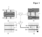
- FIG. 1 shows the application of an embodiment of the measuring method according to the invention for measuring a semiconductor device 1, which is designed as a solar cell, with two mutually parallel metallization lines 2a and 2b, which are the busbars of the metallization structure.
- a conventional photoluminescence measuring device is used, which has been extended by a modification unit with two optical filters.
- the cell is not electrically contacted during the measurement.
- a total of three measurements are carried out, with each measurement a recording with the camera of the measuring device are performed with a measuring time of one second.
- the three measurements differ only by different shading conditions with respect to the excitation radiation.
- the measuring surface is here in the FIGS. 1 a, b, c, d each shown front of the solar cell.
- a first measurement ( FIG. 1a
- the partial area which is delimited by the metallization lines 2 a and 2 b and the edges of the solar cell is shaded by the optical filters (represented by the striated marking) as the sinking partial area, so that only a partial area starting from the metallization line 2 b to to the upper edge of the solar cell and a partial area starting from the metallization line 2a to the lower edge of the solar cell are excited as exciting subregions with excitation radiation.
- this generates current flow patterns which correspond to a contacted solar cell in which charge carriers are removed from these metallization lines into an external circuit by electrical contacting of the metallization lines 2a and 2b and, accordingly, lateral current flows to the metallization lines in the solar cell.
- a measurement image is taken with inverted illumination, ie, in a second step A, the two outer subregions are shaded as Senkenteil Schemee (indicated by the strikethemark) and the central portion, which through the metallization lines 2a and 2b, and the right and left edge the solar cell is limited, is acted as excitation subregion with excitation radiation.
- the effect occurs that in the solar cell lateral currents in the direction of the metallization 2 a and 2 b arise and thus the state of an electrically contacted solar cell for the central portion of the solar cell is simulated.
- the contacting portions as previously described are defined only as those portions which are covered by the busbars but not by the metallizing fingers.
- the measuring surface is segmented by the contacting subregions and in each step A each excitation subregions covers one segment each, the respective adjacent segments being covered by depression subareas.
- the excitation and sink subregions are respectively bounded by the edges of the solar cell and the contacting subregions and each have the maximum extent within these limits.
- the maximum extent it is disregarded that the busbars do not come close to the edges of the solar cell, but a slight distance from the latter.
- the delimitation by the Kunststoff Industriessteil Schemee is supplemented in the slight distance between the ends of the busbars and the solar cell edges by an imaginary extension of the Needlessteilsteil Kunststoffe to the solar cell edges.
- a spatially resolved image of the photoluminescence radiation is recorded in each case by means of the camera of the measuring device.
- a third measurement in a step A ', the entire solar cell is exposed to excitation radiation, without shading the excitation radiation takes place.
- These three measurement images are calculated in accordance with the formula 1 given above for each measurement point in an evaluation step:
- the first two measurement images are added in terms of measurement intensity (indicated by the triangle symbol with "+”), so that a spatially resolved measurement image of the entire solar cell with Stromtikmustern respectively to the metallization lines 2a and 2b.
- the spatially resolved measurement image of the third measurement is subtracted for each location point (triangular symbol with "-"), in which case the logarithmic measured values are used according to Formula 1.
- the measuring method according to the invention it is thus possible for the first time to carry out measurements under an electrically non-contacted solar cell under conditions which correspond to a solar cell connected to an external circuit with removal of charge carriers, in particular from the metallization lines of the solar cell.
- the measuring method according to the invention and the measuring device according to the invention are particularly suitable for inline operation, d. H. for the continuous characterization of the solar cells produced in a production line, without having to remove the solar cell to be measured from the production flow for this purpose.
Landscapes
- Physics & Mathematics (AREA)
- Health & Medical Sciences (AREA)
- Electromagnetism (AREA)
- Toxicology (AREA)
- General Physics & Mathematics (AREA)
- Testing Or Measuring Of Semiconductors Or The Like (AREA)
- Investigating, Analyzing Materials By Fluorescence Or Luminescence (AREA)
- Testing Of Individual Semiconductor Devices (AREA)
- Photometry And Measurement Of Optical Pulse Characteristics (AREA)
Claims (16)
- Procédé de mesure ciblant la caractérisation d'un composant (1) à semi-conducteurs présentant au moins une jonction pn et une surface de mesure matérialisée par la face antérieure et/ou la face postérieure dudit composant à semi-conducteurs, et comportant au moins une région partielle de mise en contact qui est recouverte par une structure de mise en contact, ou est prévue pour le recouvrement par une structure de mise en contact, comprenant les étapes suivantes :A sollicitation du plan de la surface de mesure du composant (1) à semi-conducteurs par un rayonnement excitateur électromagnétique, en vue de la séparation de paires de porteurs de charge dans ledit composant (1) à semi-conducteurs, etB mesure à résolution spatiale d'un rayonnement électromagnétique provenant dudit composant (1) à semi-conducteurs, à l'aide d'au moins une unité de détection,sachant que, lors d'au moins une étape A, au moins une zone d'excitation partielle préétablie de ladite surface de mesure est sollicitée par une intensité du rayonnement excitateur préétablie pour cette zone d'excitation partielle, et au moins une zone partielle de puits de ladite surface de mesure est sollicitée par une intensité dudit rayonnement excitateur qui est moindre comparativement à ladite zone d'excitation partielle, et/ou sachant que l'intensité 0 affectée audit rayonnement excitateur est préétablie, pour au moins une zone partielle de puits préétablie, de façon telle qu'au moins une zone partielle de puits ne soit pas sollicitée par un rayonnement excitateur, lors d'une étape A, caractérisé par le fait
que des zones partielles d'excitation et de puits se trouvent sur des côtés opposés de la région partielle de mise en contact et sont limitrophes de cette dernière, et/ou chevauchent cette dernière en totalité ou en partie. - Procédé selon la revendication 1,
caractérisé par le fait
que la surface de mesure est scindée en des segments par une ou plusieurs région(s) partielle(s) de mise en contact,
que, lors d'au moins une étape A, au moins une zone d'excitation partielle recouvre au moins un segment, de préférence exactement un segment, et les segments voisins de cette zone d'excitation partielle sont recouverts par des zones partielles de puits. - Procédé selon au moins l'une des revendications précédentes,
caractérisé par le fait
que, lors d'au moins une étape A, au moins une zone d'excitation partielle présente une délimitation commune avec la région partielle de mise en contact, de préférence que, durant toutes les étapes A, toutes les zones d'excitation partielles présentent une délimitation commune avec une région partielle de mise en contact respectivement préétablie. - Procédé selon la revendication 3,
caractérisé par le fait
que la zone d'excitation partielle s'étend le long d'un côté de la région partielle de mise en contact, notamment
que, durant toutes les étapes A, toutes les zones d'excitation partielles s'étendent le long d'un côté d'une région partielle de mise en contact respectivement préétablie. - Procédé selon l'une des revendications précédentes,
caractérisé par le fait
que, lors d'au moins une étape A, au moins une zone d'excitation partielle est délimitée par le bord de la région partielle de mise en contact, ainsi qu'en outre par d'autres régions partielles préétablies de mise en contact et/ou, en outre, par un ou plusieurs bord(s) du composant à semi-conducteurs. - Procédé selon au moins l'une des revendications précédentes,
caractérisé par le fait
que la région partielle de mise en contact est une région partielle de mise en contact de barre omnibus, recouverte par une barre omnibus ou prévue pour le recouvrement par une barre omnibus, notamment
que le composant à semi-conducteurs présente une pluralité de b régions partielles de mise en contact de barres omnibus et,
durant chaque étape A, au moins 1/(2b), de préférence au moins 1/b de la superficie de la surface de mesure est recouvert par la ou les zone(s) d'excitation partielle(s). - Procédé selon au moins l'une des revendications précédentes,
caractérisé par le fait
que, durant chaque étape A, au moins 1/6, de préférence au moins 1/4 de la superficie de la surface de mesure est recouvert par la ou les zone(s) d'excitation partielle(s), notamment
que, durant chaque étape A, sensiblement la moitié de la superficie de ladite surface de mesure est recouverte par la ou les zone(s) d'excitation partielle(s). - Procédé selon au moins l'une des revendications précédentes,
caractérisé par le fait
que l'étape A est exécutée au moins deux fois, sachant qu'il s'opère respectivement une mesure conforme à l'étape B, et que les étapes A présentent différentes zones d'excitation partielles. - Procédé selon au moins l'une des revendications précédentes,
caractérisé par le fait
que toutes les zones d'excitation partielles de toutes les étapes A, prises ensemble, recouvrent au moins la surface de mesure à l'extérieur des régions partielles de mise en contact, notamment
que toutes les zones d'excitation partielles de toutes les étapes A, prises ensemble, recouvrent l'intégralité de ladite surface de mesure. - Procédé selon au moins l'une des revendications précédentes,
caractérisé par le fait
que l'intensité 0 est préétablie pour toutes les zones partielles de puits. - Procédé selon au moins l'une des revendications précédentes,
caractérisé par le fait
que, durant chaque étape A, des zones d'excitation partielles et des zones partielles de puits recouvrent, prises ensemble, au moins la surface de mesure à l'extérieur des régions partielles de mise en contact et recouvrent, en particulier, l'intégralité de ladite surface de mesure. - Procédé selon l'une des revendications précédentes,
caractérisé par le fait
que les zones d'excitation partielles de toutes les étapes A sont dissociées, notamment dissociées par paires, et/ou
que, lors d'au moins une étape A, toutes les zones d'excitation partielles sont convexes, notamment que toutes lesdites zones d'excitation partielles sont convexes durant toutes les étapes A. - Procédé selon au moins l'une des revendications précédentes,
caractérisé par le fait
que, lors d'une autre étape A', la (les) face(s) antérieure et/ou postérieure du composant (1) à semi-conducteurs, de préférence la surface de mesure, est (sont) sollicitée(s) par un rayonnement excitateur sur toute la superficie, et de manière homogène quant à l'intensité dudit rayonnement, et il s'opère une mesure conforme à l'étape B, notamment que des mesures au nombre total de trois sont effectuées, sachant que différentes zones partielles sont sollicitées par un rayonnement excitateur lors de deux mesures et que, lors d'une troisième mesure, ledit composant (1) à semi-conducteurs est sollicité par un rayonnement excitateur sur toute la superficie, et de manière homogène, notamment qu'une interprétation conforme à la formule 1 est effectuée pour chaque point localisé i, lors d'une étape d'interprétation,
c'est-à-dire que, pour un nombre total de n points de mesure, le résultat MEi de la mesure est déterminé pour chaque point localisé i, conformément à ladite formule 1, en fonction des valeurs mesurées relatives au point localisé i résultant de la première mesure M1 i , de la deuxième mesure M2 i et de la troisième mesure M3 i . - Procédé selon au moins l'une des revendications précédentes,
caractérisé par le fait
que les étapes A et B sont exécutées en simultanéité. - Dispositif de mesure dévolu à un composant (1) à semi-conducteurs muni d'une face antérieure et d'une face postérieure, comprenant
une source de rayonnement destinée à la sollicitation du plan de la (des) face(s) antérieure et/ou postérieure dudit composant (1) à semi-conducteurs par un rayonnement excitateur,
et
une unité de détection dédiée à la mesure à résolution spatiale d'un rayonnement électromagnétique provenant dudit composant (1) à semi-conducteurs,
lequel dispositif de mesure inclut, par ailleurs, une unité de modification interposée entre le composant (1) à semi-conducteurs et la source de rayonnement, sur le trajet des rayons de ladite source de rayonnement, et
ladite unité de modification comportant au moins un filtre optique pouvant être sélectivement placé sur le trajet des rayons entre ladite source de rayonnement et ledit composant (1) à semi-conducteurs, ledit filtre optique permettant d'influencer l'intensité et/ou la composition spectrale du rayon de ladite source de rayonnement dans des zones partielles préétablies,
caractérisé par le fait
que ledit dispositif de mesure est conçu en vue de la caractérisation d'un composant à semi-conducteurs présentant une surface de mesure matérialisée par la face antérieure et/ou la face postérieure dudit composant à semi-conducteurs, et comportant au moins une région partielle de mise en contact qui est recouverte par une structure de mise en contact, ou est prévue pour le recouvrement par une structure de mise en contact,
du fait que ladite unité de modification est réalisée de telle sorte qu'au moins une zone d'excitation partielle préétablie de ladite surface de mesure puisse être sollicitée par une intensité du rayonnement excitateur préétablie pour cette zone d'excitation partielle, et qu'au moins une zone partielle de puits de ladite surface de mesure puisse être sollicitée par une intensité dudit rayonnement excitateur qui est moindre comparativement à ladite zone d'excitation partielle, et/ou que l'intensité 0 affectée audit rayonnement excitateur puisse être préétablie pour au moins une zone partielle de puits préétablie, sachant que des zones partielles d'excitation et de puits se trouvent sur des côtés opposés de la région partielle de mise en contact et sont limitrophes de cette dernière, et/ou chevauchent cette dernière en totalité ou en partie. - Dispositif selon la revendication 15,
caractérisé par le fait
que l'unité de modification est pourvue d'un support sur lequel au moins un filtre optique est implanté avec aptitude pivotante, de manière à pouvoir sélectivement pivoter vers une position parallèle, et vers une position perpendiculaire à l'axe principal du rayon de la source de rayonnement, notamment
que ladite unité de modification inclut un dispositif de pivotement en liaison interactive avec ledit filtre optique, de manière à imprimer des pivotements audit filtre optique vis-à-vis dudit axe principal du rayon de ladite source de rayonnement, notamment que ledit dispositif de pivotement peut être commandé au moyen de signaux électriques de commande, et/ou
que le dispositif, affecté à la mesure d'un composant (1) à semi-conducteurs, est doté d'au moins une ligne de métallisation (2a, 2b) et ledit filtre optique occupe, sur ladite unité de modification, une position telle que, lors d'un alignement dudit filtre optique parallèlement audit axe principal du rayon de ladite source de rayonnement, l'occultation persistante, provoquée par ce filtre, concerne sensiblement une zone partielle du rayon de ladite source de rayonnement à laquelle est associée ladite ligne de métallisation (2a, 2b) de type linéaire.
Applications Claiming Priority (2)
| Application Number | Priority Date | Filing Date | Title |
|---|---|---|---|
| DE102008010672 | 2008-02-22 | ||
| PCT/EP2009/001277 WO2009103566A2 (fr) | 2008-02-22 | 2009-02-23 | Procédé de mesure et dispositif pour caractériser un composant à semi-conducteurs |
Publications (2)
| Publication Number | Publication Date |
|---|---|
| EP2245473A2 EP2245473A2 (fr) | 2010-11-03 |
| EP2245473B1 true EP2245473B1 (fr) | 2012-08-29 |
Family
ID=40985975
Family Applications (1)
| Application Number | Title | Priority Date | Filing Date |
|---|---|---|---|
| EP09712988A Active EP2245473B1 (fr) | 2008-02-22 | 2009-02-23 | Procédé de mesure et dispositif pour caractériser un composant à semi-conducteurs |
Country Status (6)
| Country | Link |
|---|---|
| US (1) | US8829938B2 (fr) |
| EP (1) | EP2245473B1 (fr) |
| JP (1) | JP5489107B2 (fr) |
| CN (1) | CN101971040B (fr) |
| AU (1) | AU2009216934B2 (fr) |
| WO (1) | WO2009103566A2 (fr) |
Cited By (2)
| Publication number | Priority date | Publication date | Assignee | Title |
|---|---|---|---|---|
| DE102020119323B3 (de) | 2020-07-22 | 2021-11-18 | Albert-Ludwigs-Universität Freiburg, Körperschaft des öffentlichen Rechts | Verfahren zur Analyse einer Vielzahl von optischen Halbleiterbauelementen |
| DE102020133701A1 (de) | 2020-12-16 | 2022-06-23 | Fraunhofer-Gesellschaft zur Förderung der angewandten Forschung eingetragener Verein | Verfahren und Vorrichtung zur Qualitätsbewertung einer Solarzelle |
Families Citing this family (12)
| Publication number | Priority date | Publication date | Assignee | Title |
|---|---|---|---|---|
| DE102009039399A1 (de) * | 2009-08-31 | 2011-03-03 | Fraunhofer-Gesellschaft zur Förderung der angewandten Forschung e.V. | Verfahren zur Vermessung einer Halbleiterstruktur, welche eine Solarzelle oder eine Vorstufe einer Solarzelle ist |
| JP4944231B2 (ja) * | 2010-08-11 | 2012-05-30 | コニカミノルタセンシング株式会社 | 太陽電池評価装置およびそれに用いられる光源評価装置 |
| US20140039820A1 (en) * | 2011-04-18 | 2014-02-06 | Bt Imaging Pty Ltd | Quantitative series resistance imaging of photovoltaic cells |
| WO2014005185A1 (fr) | 2012-07-06 | 2014-01-09 | Bt Imaging Pty Ltd | Procédés de contrôle de tranches de semiconducteurs |
| CN103474370B (zh) * | 2013-09-13 | 2018-04-06 | 上海集成电路研发中心有限公司 | 铜线阵区域抛光后表面凹陷的测量单元及测量方法 |
| US9921261B2 (en) * | 2013-10-17 | 2018-03-20 | Kla-Tencor Corporation | Method and apparatus for non-contact measurement of sheet resistance and shunt resistance of p-n junctions |
| JP6418542B2 (ja) * | 2013-12-10 | 2018-11-07 | 株式会社Screenホールディングス | 検査装置および検査方法 |
| US9641125B2 (en) | 2015-01-23 | 2017-05-02 | Alliance For Sustainable Energy, Llc | Luminescence imaging systems and methods for evaluating photovoltaic devices |
| US10554172B2 (en) | 2017-03-09 | 2020-02-04 | Alliance For Sustainable Energy, Llc | Illuminated outdoor luminescence imaging of photovoltaic modules |
| RU174672U1 (ru) * | 2017-04-18 | 2017-10-25 | Акционерное общество "Оптрон" | Устройство измерения статических параметров полупроводниковых приборов |
| RU182112U1 (ru) * | 2017-12-20 | 2018-08-03 | Общество с ограниченной ответственностью "Газпром трансгаз Ухта" | Прибор-тестер электронных компонентов |
| KR102418633B1 (ko) * | 2021-12-22 | 2022-07-07 | 큐알티 주식회사 | 반도체 소자의 방사선 평가 방법, 및 반도체 소자의 방사선 평가 시스템 |
Family Cites Families (9)
| Publication number | Priority date | Publication date | Assignee | Title |
|---|---|---|---|---|
| AU716040B2 (en) * | 1993-06-24 | 2000-02-17 | Bausch & Lomb Incorporated | Ophthalmic pachymeter and method of making ophthalmic determinations |
| JP3647209B2 (ja) * | 1997-06-30 | 2005-05-11 | キヤノン株式会社 | 太陽電池特性の測定方法 |
| TW200707719A (en) * | 2005-06-30 | 2007-02-16 | Koninkl Philips Electronics Nv | Method for reducing occurrence of short-circuit failure in an organic functional device |
| DE102005040010A1 (de) * | 2005-08-23 | 2007-03-15 | Rwe Schott Solar Gmbh | Verfahren und Vorrichtung zur Ermittlung von Produktionsfehlern in einem Halbleiterbau-element |
| TR201802704T4 (tr) | 2005-10-11 | 2018-03-21 | Bt Imaging Pty Ltd | Dolaylı bant aralığı yarı iletken yapısının denetlenmesi için metot ve sistem. |
| DE102006006411A1 (de) * | 2006-02-09 | 2007-08-16 | Friedrich-Alexander-Universität Erlangen-Nürnberg | Anordnungen und Verfahren zur Bestimmung von Dosismessgrößen und zur Ermittlung von Energieinformation einfallender Strahlung aus Photonen oder geladenen Teilchen mit zählenden Detektoreinheiten |
| WO2007128060A1 (fr) * | 2006-05-05 | 2007-11-15 | Bt Imaging Pty Ltd | Procédé et système pour tester des dispositifs semi-conducteurs à bande interdite indirecte au moyen de l'imagerie de luminescence |
| US7919762B2 (en) * | 2006-08-01 | 2011-04-05 | Bt Imaging Pty Ltd | Determining diffusion length of minority carriers using luminescence |
| JP5077872B2 (ja) * | 2007-03-13 | 2012-11-21 | 独立行政法人 宇宙航空研究開発機構 | 太陽電池のフォトルミネセンスによる欠陥検査装置及び方法 |
-
2009
- 2009-02-23 CN CN200980106174.3A patent/CN101971040B/zh active Active
- 2009-02-23 JP JP2010547123A patent/JP5489107B2/ja not_active Expired - Fee Related
- 2009-02-23 AU AU2009216934A patent/AU2009216934B2/en active Active
- 2009-02-23 WO PCT/EP2009/001277 patent/WO2009103566A2/fr active Application Filing
- 2009-02-23 US US12/918,921 patent/US8829938B2/en active Active
- 2009-02-23 EP EP09712988A patent/EP2245473B1/fr active Active
Cited By (3)
| Publication number | Priority date | Publication date | Assignee | Title |
|---|---|---|---|---|
| DE102020119323B3 (de) | 2020-07-22 | 2021-11-18 | Albert-Ludwigs-Universität Freiburg, Körperschaft des öffentlichen Rechts | Verfahren zur Analyse einer Vielzahl von optischen Halbleiterbauelementen |
| DE102020133701A1 (de) | 2020-12-16 | 2022-06-23 | Fraunhofer-Gesellschaft zur Förderung der angewandten Forschung eingetragener Verein | Verfahren und Vorrichtung zur Qualitätsbewertung einer Solarzelle |
| WO2022129172A1 (fr) | 2020-12-16 | 2022-06-23 | Fraunhofer-Gesellschaft zur Förderung der angewandten Forschung e. V. | Procédé et dispositif permettant l'évaluation de la qualité d'une cellule solaire |
Also Published As
| Publication number | Publication date |
|---|---|
| WO2009103566A2 (fr) | 2009-08-27 |
| US20110012636A1 (en) | 2011-01-20 |
| CN101971040B (zh) | 2014-11-26 |
| EP2245473A2 (fr) | 2010-11-03 |
| JP5489107B2 (ja) | 2014-05-14 |
| AU2009216934A1 (en) | 2009-08-27 |
| WO2009103566A3 (fr) | 2009-12-17 |
| JP2011512537A (ja) | 2011-04-21 |
| US8829938B2 (en) | 2014-09-09 |
| CN101971040A (zh) | 2011-02-09 |
| AU2009216934B2 (en) | 2014-07-17 |
Similar Documents
| Publication | Publication Date | Title |
|---|---|---|
| EP2245473B1 (fr) | Procédé de mesure et dispositif pour caractériser un composant à semi-conducteurs | |
| EP2473839B1 (fr) | Procédé de mesure d'une structure semi-conductrice sous la forme d'une cellule solaire ou d'une ébauche de cellule solaire | |
| DE69631417T2 (de) | Methode zur identifizierung molekularer substanzen | |
| DE112015001642B4 (de) | Verfahren zur Lochbildung und Messvorrichtung | |
| EP2115435B1 (fr) | Procédé et agencement pour la détection de défauts mécaniques d'un composant semi-conducteur, notamment d'une pile solaire ou d'un agencement de piles solaires | |
| DD254998A1 (de) | Anordnung zur bildlichen darstellung und analyse von fluoreszenzsignalen | |
| DE2125456B2 (de) | Verfahren zur Ermittlung des Schichtwiderstandes oder einer hiermit zusammenhängenden Größe, insbesondere bei der Herstellung einer Halbleiteranordnung, Anwendung dieses Verfahrens sowie Meßvorrichtung zum Durchführen dieses Verfahrens | |
| EP2433148B1 (fr) | Procédé pour déterminer spatialement la résistance série d'une structure semi-conductrice | |
| DE102016218920A1 (de) | Dual-Energy-Detektionsvorrichtung, Dual-Energy-Detektionssystem und Dual-Energy-Detektionsverfahren | |
| DE112017006630T5 (de) | SiC-Wafer-Fehlermessverfahren, Referenzprobe und Verfahren zur Herstellung eines Epitaxialen SiC-Wafers | |
| EP1416288B1 (fr) | Procédé et dispositif de détection optique des défauts mécaniques dans des dispositifs à semi-conducteur, notamment pour systèmes de cellules solaires | |
| DE2544296A1 (de) | Verfahren und vorrichtung zur bestimmung der mittleren lochgroesse in einem gelochten koerper | |
| WO2010022922A1 (fr) | Procédé pour la détermination de la durée de vie d’un porteur de surcharge dans une couche semi-conductrice | |
| EP2331942A1 (fr) | Procédé de mesure pour une structure semi-conductrice | |
| CH711709B1 (de) | Verfahren und Vorrichtung zur Prüfung der Kontaktierungsgüte eines elektrischen Kontaktes zwischen einer Solarzelle und einer Kontaktierungseinheit. | |
| DE102018005152A1 (de) | Methode zur Hochdurchsatz-Charakterisierung von elektrischen, elektronischen, optoelektronischen und elektrochemischen Dünnschicht-Bauelementen und Verfahren zu deren Herstellung | |
| EP2318851B1 (fr) | Procédé permettant de déterminer les propriétés de recombinaison au niveau d'une zone partielle de mesure d'un côté de mesure d'une structure semi-conductrice | |
| DE102017221719B4 (de) | Optisches emissionsspektrometer mit kaskadierten ladungsspeichern | |
| DE1598130C3 (de) | Verfahren und Vorrichtung zur Materialanalyse in einem Sekundär-Elektronen-Emissions-Mikroskop | |
| DE202023105215U1 (de) | Solarmodul | |
| DE202023105214U1 (de) | Solarmodul | |
| DE102010006074A1 (de) | Vorrichtung und Verfahren zur Charakterisierung einer elektrischen Eigenschaft eines Schichtmaterials | |
| DE202023105213U1 (de) | Solarmodul | |
| DE102009003544A1 (de) | Verfahren zur Überprüfung von Solarzellenoberflächen | |
| DE102019100615A1 (de) | Verfahren und Vorrichtung zur Erfassung einer Beschichtung auf einer Oberfläche |
Legal Events
| Date | Code | Title | Description |
|---|---|---|---|
| PUAI | Public reference made under article 153(3) epc to a published international application that has entered the european phase |
Free format text: ORIGINAL CODE: 0009012 |
|
| 17P | Request for examination filed |
Effective date: 20100811 |
|
| AK | Designated contracting states |
Kind code of ref document: A2 Designated state(s): AT BE BG CH CY CZ DE DK EE ES FI FR GB GR HR HU IE IS IT LI LT LU LV MC MK MT NL NO PL PT RO SE SI SK TR |
|
| AX | Request for extension of the european patent |
Extension state: AL BA RS |
|
| RIN1 | Information on inventor provided before grant (corrected) |
Inventor name: FOELL, HELMUT Inventor name: WARTA, WILHELM Inventor name: KASEMANN, MARTIN Inventor name: CARSTENSEN, JUERGEN Inventor name: SCHUETT, ANDREAS |
|
| DAX | Request for extension of the european patent (deleted) | ||
| 17Q | First examination report despatched |
Effective date: 20111121 |
|
| GRAP | Despatch of communication of intention to grant a patent |
Free format text: ORIGINAL CODE: EPIDOSNIGR1 |
|
| GRAS | Grant fee paid |
Free format text: ORIGINAL CODE: EPIDOSNIGR3 |
|
| GRAA | (expected) grant |
Free format text: ORIGINAL CODE: 0009210 |
|
| AK | Designated contracting states |
Kind code of ref document: B1 Designated state(s): AT BE BG CH CY CZ DE DK EE ES FI FR GB GR HR HU IE IS IT LI LT LU LV MC MK MT NL NO PL PT RO SE SI SK TR |
|
| REG | Reference to a national code |
Ref country code: GB Ref legal event code: FG4D Free format text: NOT ENGLISH |
|
| REG | Reference to a national code |
Ref country code: CH Ref legal event code: EP |
|
| REG | Reference to a national code |
Ref country code: AT Ref legal event code: REF Ref document number: 573337 Country of ref document: AT Kind code of ref document: T Effective date: 20120915 |
|
| REG | Reference to a national code |
Ref country code: IE Ref legal event code: FG4D Free format text: LANGUAGE OF EP DOCUMENT: GERMAN |
|
| REG | Reference to a national code |
Ref country code: DE Ref legal event code: R096 Ref document number: 502009004538 Country of ref document: DE Effective date: 20121025 |
|
| REG | Reference to a national code |
Ref country code: CH Ref legal event code: NV Representative=s name: R. A. EGLI AND CO. PATENTANWAELTE, CH |
|
| REG | Reference to a national code |
Ref country code: NL Ref legal event code: VDEP Effective date: 20120829 |
|
| REG | Reference to a national code |
Ref country code: LT Ref legal event code: MG4D Effective date: 20120829 |
|
| PG25 | Lapsed in a contracting state [announced via postgrant information from national office to epo] |
Ref country code: IS Free format text: LAPSE BECAUSE OF FAILURE TO SUBMIT A TRANSLATION OF THE DESCRIPTION OR TO PAY THE FEE WITHIN THE PRESCRIBED TIME-LIMIT Effective date: 20121229 Ref country code: HR Free format text: LAPSE BECAUSE OF FAILURE TO SUBMIT A TRANSLATION OF THE DESCRIPTION OR TO PAY THE FEE WITHIN THE PRESCRIBED TIME-LIMIT Effective date: 20120829 Ref country code: NO Free format text: LAPSE BECAUSE OF FAILURE TO SUBMIT A TRANSLATION OF THE DESCRIPTION OR TO PAY THE FEE WITHIN THE PRESCRIBED TIME-LIMIT Effective date: 20121129 Ref country code: LT Free format text: LAPSE BECAUSE OF FAILURE TO SUBMIT A TRANSLATION OF THE DESCRIPTION OR TO PAY THE FEE WITHIN THE PRESCRIBED TIME-LIMIT Effective date: 20120829 Ref country code: FI Free format text: LAPSE BECAUSE OF FAILURE TO SUBMIT A TRANSLATION OF THE DESCRIPTION OR TO PAY THE FEE WITHIN THE PRESCRIBED TIME-LIMIT Effective date: 20120829 |
|
| PG25 | Lapsed in a contracting state [announced via postgrant information from national office to epo] |
Ref country code: SI Free format text: LAPSE BECAUSE OF FAILURE TO SUBMIT A TRANSLATION OF THE DESCRIPTION OR TO PAY THE FEE WITHIN THE PRESCRIBED TIME-LIMIT Effective date: 20120829 Ref country code: GR Free format text: LAPSE BECAUSE OF FAILURE TO SUBMIT A TRANSLATION OF THE DESCRIPTION OR TO PAY THE FEE WITHIN THE PRESCRIBED TIME-LIMIT Effective date: 20121130 Ref country code: SE Free format text: LAPSE BECAUSE OF FAILURE TO SUBMIT A TRANSLATION OF THE DESCRIPTION OR TO PAY THE FEE WITHIN THE PRESCRIBED TIME-LIMIT Effective date: 20120829 Ref country code: PT Free format text: LAPSE BECAUSE OF FAILURE TO SUBMIT A TRANSLATION OF THE DESCRIPTION OR TO PAY THE FEE WITHIN THE PRESCRIBED TIME-LIMIT Effective date: 20121231 Ref country code: LV Free format text: LAPSE BECAUSE OF FAILURE TO SUBMIT A TRANSLATION OF THE DESCRIPTION OR TO PAY THE FEE WITHIN THE PRESCRIBED TIME-LIMIT Effective date: 20120829 |
|
| PG25 | Lapsed in a contracting state [announced via postgrant information from national office to epo] |
Ref country code: DK Free format text: LAPSE BECAUSE OF FAILURE TO SUBMIT A TRANSLATION OF THE DESCRIPTION OR TO PAY THE FEE WITHIN THE PRESCRIBED TIME-LIMIT Effective date: 20120829 Ref country code: CZ Free format text: LAPSE BECAUSE OF FAILURE TO SUBMIT A TRANSLATION OF THE DESCRIPTION OR TO PAY THE FEE WITHIN THE PRESCRIBED TIME-LIMIT Effective date: 20120829 Ref country code: RO Free format text: LAPSE BECAUSE OF FAILURE TO SUBMIT A TRANSLATION OF THE DESCRIPTION OR TO PAY THE FEE WITHIN THE PRESCRIBED TIME-LIMIT Effective date: 20120829 Ref country code: ES Free format text: LAPSE BECAUSE OF FAILURE TO SUBMIT A TRANSLATION OF THE DESCRIPTION OR TO PAY THE FEE WITHIN THE PRESCRIBED TIME-LIMIT Effective date: 20121210 Ref country code: NL Free format text: LAPSE BECAUSE OF FAILURE TO SUBMIT A TRANSLATION OF THE DESCRIPTION OR TO PAY THE FEE WITHIN THE PRESCRIBED TIME-LIMIT Effective date: 20120829 Ref country code: EE Free format text: LAPSE BECAUSE OF FAILURE TO SUBMIT A TRANSLATION OF THE DESCRIPTION OR TO PAY THE FEE WITHIN THE PRESCRIBED TIME-LIMIT Effective date: 20120829 |
|
| PG25 | Lapsed in a contracting state [announced via postgrant information from national office to epo] |
Ref country code: IT Free format text: LAPSE BECAUSE OF FAILURE TO SUBMIT A TRANSLATION OF THE DESCRIPTION OR TO PAY THE FEE WITHIN THE PRESCRIBED TIME-LIMIT Effective date: 20120829 Ref country code: SK Free format text: LAPSE BECAUSE OF FAILURE TO SUBMIT A TRANSLATION OF THE DESCRIPTION OR TO PAY THE FEE WITHIN THE PRESCRIBED TIME-LIMIT Effective date: 20120829 Ref country code: PL Free format text: LAPSE BECAUSE OF FAILURE TO SUBMIT A TRANSLATION OF THE DESCRIPTION OR TO PAY THE FEE WITHIN THE PRESCRIBED TIME-LIMIT Effective date: 20120829 |
|
| PLBE | No opposition filed within time limit |
Free format text: ORIGINAL CODE: 0009261 |
|
| STAA | Information on the status of an ep patent application or granted ep patent |
Free format text: STATUS: NO OPPOSITION FILED WITHIN TIME LIMIT |
|
| PG25 | Lapsed in a contracting state [announced via postgrant information from national office to epo] |
Ref country code: BG Free format text: LAPSE BECAUSE OF FAILURE TO SUBMIT A TRANSLATION OF THE DESCRIPTION OR TO PAY THE FEE WITHIN THE PRESCRIBED TIME-LIMIT Effective date: 20121129 |
|
| 26N | No opposition filed |
Effective date: 20130530 |
|
| BERE | Be: lapsed |
Owner name: CHRISTIAN-ALBRECHTS-UNIVERSITAT ZU KIEL Effective date: 20130228 Owner name: ALBERT-LUDWIGS-UNIVERSITAT FREIBURG Effective date: 20130228 Owner name: FRAUNHOFER-GESELLSCHAFT ZUR FORDERUNG DER ANGEWAN Effective date: 20130228 |
|
| REG | Reference to a national code |
Ref country code: DE Ref legal event code: R097 Ref document number: 502009004538 Country of ref document: DE Effective date: 20130530 |
|
| PG25 | Lapsed in a contracting state [announced via postgrant information from national office to epo] |
Ref country code: MC Free format text: LAPSE BECAUSE OF NON-PAYMENT OF DUE FEES Effective date: 20130228 |
|
| PG25 | Lapsed in a contracting state [announced via postgrant information from national office to epo] |
Ref country code: CY Free format text: LAPSE BECAUSE OF FAILURE TO SUBMIT A TRANSLATION OF THE DESCRIPTION OR TO PAY THE FEE WITHIN THE PRESCRIBED TIME-LIMIT Effective date: 20120829 |
|
| REG | Reference to a national code |
Ref country code: IE Ref legal event code: MM4A |
|
| PG25 | Lapsed in a contracting state [announced via postgrant information from national office to epo] |
Ref country code: BE Free format text: LAPSE BECAUSE OF NON-PAYMENT OF DUE FEES Effective date: 20130228 Ref country code: IE Free format text: LAPSE BECAUSE OF NON-PAYMENT OF DUE FEES Effective date: 20130223 |
|
| PG25 | Lapsed in a contracting state [announced via postgrant information from national office to epo] |
Ref country code: MT Free format text: LAPSE BECAUSE OF FAILURE TO SUBMIT A TRANSLATION OF THE DESCRIPTION OR TO PAY THE FEE WITHIN THE PRESCRIBED TIME-LIMIT Effective date: 20120829 |
|
| REG | Reference to a national code |
Ref country code: AT Ref legal event code: MM01 Ref document number: 573337 Country of ref document: AT Kind code of ref document: T Effective date: 20140223 |
|
| PG25 | Lapsed in a contracting state [announced via postgrant information from national office to epo] |
Ref country code: AT Free format text: LAPSE BECAUSE OF NON-PAYMENT OF DUE FEES Effective date: 20140223 |
|
| PG25 | Lapsed in a contracting state [announced via postgrant information from national office to epo] |
Ref country code: TR Free format text: LAPSE BECAUSE OF FAILURE TO SUBMIT A TRANSLATION OF THE DESCRIPTION OR TO PAY THE FEE WITHIN THE PRESCRIBED TIME-LIMIT Effective date: 20120829 |
|
| PG25 | Lapsed in a contracting state [announced via postgrant information from national office to epo] |
Ref country code: HU Free format text: LAPSE BECAUSE OF FAILURE TO SUBMIT A TRANSLATION OF THE DESCRIPTION OR TO PAY THE FEE WITHIN THE PRESCRIBED TIME-LIMIT; INVALID AB INITIO Effective date: 20090223 Ref country code: LU Free format text: LAPSE BECAUSE OF NON-PAYMENT OF DUE FEES Effective date: 20130223 Ref country code: MK Free format text: LAPSE BECAUSE OF FAILURE TO SUBMIT A TRANSLATION OF THE DESCRIPTION OR TO PAY THE FEE WITHIN THE PRESCRIBED TIME-LIMIT Effective date: 20120829 |
|
| REG | Reference to a national code |
Ref country code: FR Ref legal event code: PLFP Year of fee payment: 8 |
|
| REG | Reference to a national code |
Ref country code: FR Ref legal event code: PLFP Year of fee payment: 9 |
|
| REG | Reference to a national code |
Ref country code: FR Ref legal event code: PLFP Year of fee payment: 10 |
|
| PGFP | Annual fee paid to national office [announced via postgrant information from national office to epo] |
Ref country code: FR Payment date: 20230217 Year of fee payment: 15 |
|
| P01 | Opt-out of the competence of the unified patent court (upc) registered |
Effective date: 20230523 |
|
| PGFP | Annual fee paid to national office [announced via postgrant information from national office to epo] |
Ref country code: DE Payment date: 20240216 Year of fee payment: 16 Ref country code: GB Payment date: 20240222 Year of fee payment: 16 Ref country code: CH Payment date: 20240301 Year of fee payment: 16 |