EP2240797B1 - Optisch-elektronische entfernungsmessvorrichtung - Google Patents
Optisch-elektronische entfernungsmessvorrichtung Download PDFInfo
- Publication number
- EP2240797B1 EP2240797B1 EP09711373.2A EP09711373A EP2240797B1 EP 2240797 B1 EP2240797 B1 EP 2240797B1 EP 09711373 A EP09711373 A EP 09711373A EP 2240797 B1 EP2240797 B1 EP 2240797B1
- Authority
- EP
- European Patent Office
- Prior art keywords
- burst
- time
- signal
- frequency
- measuring
- Prior art date
- Legal status (The legal status is an assumption and is not a legal conclusion. Google has not performed a legal analysis and makes no representation as to the accuracy of the status listed.)
- Not-in-force
Links
Images


Classifications
-
- G—PHYSICS
- G01—MEASURING; TESTING
- G01S—RADIO DIRECTION-FINDING; RADIO NAVIGATION; DETERMINING DISTANCE OR VELOCITY BY USE OF RADIO WAVES; LOCATING OR PRESENCE-DETECTING BY USE OF THE REFLECTION OR RERADIATION OF RADIO WAVES; ANALOGOUS ARRANGEMENTS USING OTHER WAVES
- G01S17/00—Systems using the reflection or reradiation of electromagnetic waves other than radio waves, e.g. lidar systems
- G01S17/02—Systems using the reflection of electromagnetic waves other than radio waves
- G01S17/06—Systems determining position data of a target
- G01S17/08—Systems determining position data of a target for measuring distance only
- G01S17/10—Systems determining position data of a target for measuring distance only using transmission of interrupted, pulse-modulated waves
-
- G—PHYSICS
- G01—MEASURING; TESTING
- G01S—RADIO DIRECTION-FINDING; RADIO NAVIGATION; DETERMINING DISTANCE OR VELOCITY BY USE OF RADIO WAVES; LOCATING OR PRESENCE-DETECTING BY USE OF THE REFLECTION OR RERADIATION OF RADIO WAVES; ANALOGOUS ARRANGEMENTS USING OTHER WAVES
- G01S17/00—Systems using the reflection or reradiation of electromagnetic waves other than radio waves, e.g. lidar systems
- G01S17/02—Systems using the reflection of electromagnetic waves other than radio waves
- G01S17/06—Systems determining position data of a target
- G01S17/08—Systems determining position data of a target for measuring distance only
- G01S17/32—Systems determining position data of a target for measuring distance only using transmission of continuous waves, whether amplitude-, frequency-, or phase-modulated, or unmodulated
- G01S17/36—Systems determining position data of a target for measuring distance only using transmission of continuous waves, whether amplitude-, frequency-, or phase-modulated, or unmodulated with phase comparison between the received signal and the contemporaneously transmitted signal
-
- G—PHYSICS
- G01—MEASURING; TESTING
- G01S—RADIO DIRECTION-FINDING; RADIO NAVIGATION; DETERMINING DISTANCE OR VELOCITY BY USE OF RADIO WAVES; LOCATING OR PRESENCE-DETECTING BY USE OF THE REFLECTION OR RERADIATION OF RADIO WAVES; ANALOGOUS ARRANGEMENTS USING OTHER WAVES
- G01S7/00—Details of systems according to groups G01S13/00, G01S15/00, G01S17/00
- G01S7/48—Details of systems according to groups G01S13/00, G01S15/00, G01S17/00 of systems according to group G01S17/00
- G01S7/483—Details of pulse systems
- G01S7/484—Transmitters
-
- G—PHYSICS
- G01—MEASURING; TESTING
- G01S—RADIO DIRECTION-FINDING; RADIO NAVIGATION; DETERMINING DISTANCE OR VELOCITY BY USE OF RADIO WAVES; LOCATING OR PRESENCE-DETECTING BY USE OF THE REFLECTION OR RERADIATION OF RADIO WAVES; ANALOGOUS ARRANGEMENTS USING OTHER WAVES
- G01S7/00—Details of systems according to groups G01S13/00, G01S15/00, G01S17/00
- G01S7/48—Details of systems according to groups G01S13/00, G01S15/00, G01S17/00 of systems according to group G01S17/00
- G01S7/491—Details of non-pulse systems
- G01S7/4912—Receivers
Definitions
- the invention relates to an optical-electronic distance measuring method according to claim 1, an optical-electronic distance measuring device according to claim 16 and a receiving circuit therefor according to claim 10.
- Optical-electronic distance measuring devices of the generic type are well known from the prior art. They have a distance measuring range of several tens of meters and are often designed as handsets. They are mainly used in building surveying or interior work, for example, for the three-dimensional measurement of rooms. Further applications for distance measuring devices are geodetic and industrial surveying.
- the basic principle of the distance measurement with the known devices is based on the evaluation of a change over time of a characteristic variable of the electromagnetic radiation emitted by the device and reflected by a targeted object.
- the distance measuring device is equipped with a transmitter for emitting an intensity-modulated radiation.
- Handheld devices are primarily optical radiation in the visible wavelength spectrum to facilitate sighting of the measurement points. The optical radiation is reflected by the targeted measurement object and detected by a built-in receiver in the device. The time delay of the received radiation with respect to the radiation emitted by the transmitter results in the distance to the measurement object.
- detectors usually pin photodiodes or avalanche photodiodes are used in the known distance measuring devices for the conversion of the reflected on the measurement object received radiation into electrical signals used.
- Very commonly used are distance measuring devices whose distance determination is based on the measuring principle of the phase measurement.
- the electrical received signal is superimposed directly on the avalanche photodiode or after a preamplifier with a mixer frequency to a low-frequency measurement signal. On this low-frequency signal, the phase is determined and compared with the phase of a reference signal. The difference between the measured phase of the low-frequency measuring signal and the phase of the reference signal is a measure of the distance of the measuring object.
- the EP-B-0 738 899 describes the behavior of laser visible light emitting diodes and the associated accuracy problems in distance measurement.
- modulate the emitted laser radiation with pulse widths less than 2 ns.
- the modulation frequency of this known device is in the range of about 50 MHz.
- a pulse power of approximately 20 mW is required in these known devices in order to achieve an average power of 1 mW, which generally ensures sufficient eye safety.
- the proposed type of modulation can still be implemented with commercially available 3 mW lasers, without having to accept greater losses in the service life of the laser due to the increased pulse power compared to continuous 3 mW operation. Due to the short pulses and the high pulse power, a short coherence length of the laser radiation is achieved. This has a reduction of the generally granulated intensity distribution of the most rough surface of the targeted measuring object reflected radiation to the episode. The granular intensity distribution is also known as speckles and influences the achievable measurement accuracy.
- the WO 02/16964 describes a method and a device for distance measurement which are based on the phase measurement of an optical measurement radiation reflected by a targeted measurement object.
- the measurement object is exposed to an intensity-modulated, optical measurement radiation emitted by a measurement device, and a part of the measurement radiation reflected by the measurement object is detected by a receiver arranged in the measurement device and converted into electrical measurement signals.
- the electrical measurement signals are then compared with a reference signal which is generated from the detection and conversion of a guided by a known reference distance measuring light component to determine from a phase difference, the distance between the measuring device and the measurement object.
- the active burst time is the time period during which a burst signal is present, whereas during a dead time no signal is applied to the laser diode as a transmitter.
- the period of the sequence of bursts and dead time is called burst period duration.
- the burst signal has a duty cycle defined as the ratio of the active burst time to the burst period duration in%.
- the burst modulation differs from a pulse modulation, in which the modulation signal over the entire duration of a measurement period quasi-continuously applied.
- burst modulation on the other hand, the modulation signal is present only during part of the measurement period, so that only during the active burst time a pulse sequence is transmitted. According to the above definition, therefore, the duty cycle is always 100% for pulse modulation, while the value for burst modulation is always less than 100%.
- the burst modulation can be done, for example, with a square-wave burst signal.
- the signal / noise ratio (S / N) can be improved. This can be explained on a simplified example of a laser with a maximum average output power of 1 mW. If a laser burst of 10% duty cycle with a peak power of 25 mW is emitted instead of the measuring radiation emitted with 2.5 mW peak power in the known devices, an average laser power of 1 mW is again obtained.
- S / N signal-to-noise ratio
- the burst modulation can in principle be done with an active burst duration, which is limited to a single peak. Conveniently, however, the active burst duration is chosen such that it becomes a duty cycle which is about 5% to about 50%, preferably about 10% to about 40%.
- the emitted measuring radiation can be modulated in particular with a modulation frequency greater than 100 MHz and a peak power greater than 10 mW.
- the higher peak powers of the laser in the burst modulation also shorten the coherence length of the emitted laser radiation, since the laser jumps through several modes with the same pulse width but higher peak power. This can have an advantageous effect on the accuracy of the measuring devices.
- the burst modulation can also lead to a simplification of the regulation of the laser power and allow a reduction of the power consumption.
- the in the WO 02/16964 have a transmitter for emitting a burst-modulated optical radiation, a receiving optics for a reflected object on the measurement object of the measuring optical object, a receiver downstream of the receiver for converting the optical radiation into electrical measurement signals, a device for generating a reference radiation, after passing through a known Reference line can be converted into electrical reference signals, a filter device for filtering interference signals and a particular digital signal processing system for examining the measurement signals and the reference signals with respect to their phase position - to determine the distance of the measurement object and make the result available to the user - on.
- the transmitter is connected to a frequency synthesizer, with which the emitted optical radiation takes place according to the burst modulation principle intensity modulation can be imprinted.
- the evaluation of the electrical measurement and reference signals is coupled to the active burst time.
- the optical reference radiation can be generated for example by a beam splitter and detected after passing through a known reference path by a separate reference receiver and converted into electrical reference signals.
- the emitted optical measuring radiation can also be routed periodically either to the measurement object or through the reference path to the receiver.
- a deflection mirror which can be pivoted periodically into the beam path can be provided for this purpose.
- a semiconductor laser diode for visible optical radiation having, for example, a wavelength in the range of about 630 nm to about 650 nm.
- Such semiconductor laser diodes are operable with the required average output powers and can in particular provide the required pulse energies with almost no loss of service life.
- the electrical measurement signals are converted by continuous or burst-shaped superposition of a high-frequency mixer frequency into low-frequency signals and filtered only during the active burst time or converted by acting as a filter transimpedance amplifier into an output voltage, so that the low-frequency signals in one of the respective phase positions the distance the signal object determining signal processing system can be further processed.
- the mixer frequency can, for example, the value of Modulation frequency of the burst signal ⁇ the frequency value of the low-frequency signal correspond.
- the filtering out of a noise can, for example, take place on the analog low-frequency signal and / or be carried out after digitalization of the signal in the digital signal processing.
- the active burst time is determined according to the WO 02/16964 chosen with advantage to about one and a half periods of the low-frequency measurement signal.
- the first third of the active burst time is needed for the filter to settle.
- the signal is then summed up only during the following two-thirds of the active burst time, which corresponds to a complete period of the low-frequency measurement signal.
- the relatively long duration which is needed to settle the filter, has a disadvantage, since therefore - contrary to the actual idea of the burst modulation principle - as well as a relatively long active burst time must be selected.
- the actually achievable by the burst modulation advantages - in particular with regard to an improvement of the signal / noise ratio (S / N) - are thus by in the WO 02/16964 described distance measuring device only partially feasible.
- Another object of the invention is to provide an improved optical-electronic distance measuring method and an improved optical-electronic distance measuring device.
- the optical-electronic distance measuring method according to the invention is based on the principle of phase measurement of a part of a measuring radiation reflected on a measuring object.
- an optical measuring radiation modulated according to the burst modulation principle is emitted in the direction of the measurement object.
- the measuring radiation is emitted in so-called bursts.
- bursts During each active burst time, which determines the width of the bursts, while there is a modulation signal, so that the measurement radiation is emitted intensity modulated with a certain modulation frequency.
- a burst period is defined as the duration for an active burst time and a dead time such that the burst period indicates, for example, the distance between each beginning of two consecutive bursts.
- At least one part of the emitted measuring radiation which is reflected by the measuring object is received again and converted into an input measuring signal.
- a particular continuous superimposition takes place with a mixer frequency such that the input measurement signal substantially comprises burst pulses of constant width, which is determined by the active burst time, and modulated amplitude.
- the mixer signal is modulated and superimposed in such a way that a curve enveloping the burst pulses is approximately sinusoidal in the form of an LF envelope with a low-frequency LF envelope frequency in relation to the modulation frequency of the measurement radiation.
- a distance to the measurement object is determined by evaluating a measurement signal generated from the input measurement signal, which is compared with a reference signal for this purpose.
- the generated measurement signal is compared with respect to a phase position relative to a reference signal, wherein the reference signal can be generated for example from the detection and conversion of a guided by a known reference path portion of the measurement radiation.
- the measurement signal when the measurement signal is generated during a sampling time associated with the active burst time, the measurement signal is dependent on the input measurement signal and the measurement signal is essentially at a value that it has at the end of the first time period during a hold time associated with the dead time. kept constant.
- a so-called sample-and-hold member can be integrated.
- sample-and-hold circuits are well known in the prior art and are also used as sample-and-hold circuit, sample-and-hold circuit or gate (S & H) or track-and-hold circuit. -Element designated.
- the central element of a sample-and-hold circuit is usually a capacitor which takes over a memory function for the incoming analog values.
- a sample-and-hold circuit usually has an electronic switch for determining the sampling and the holding phase.
- the output of a sample-and-hold circuit corresponds to the values of the input signal while the output signal in an off state remains constant at the value that the output signal has at the time of turn-off.
- the sample-and-hold element can now be switched on at the beginning of the active burst time of the received measurement radiation and switched off at the beginning of a dead time of the received measurement radiation.
- the charging process of the capacitor caused by the input signal can be designed after switching on the sample-and-hold element, which also influences, for example, the response time of the sample-and-hold element.
- the set-up time is understood to mean that time until the voltage at the capacitor after switching on the sample-and-hold element corresponds to the input voltage, within a certain tolerance. For example, if the sample-and-hold circuit has a low bandwidth, then the capacitor voltage determining the output signal will only slightly approximate the value of the incoming burst pulse during the sampling time associated with the active burst time, whereas at very high bandwidths, the capacitor of the sample -Hold member is fully charged to the value of the incoming burst.
- the distance measuring method triggers the fact that the low-frequency burst pulses generated by superimposing a mixer signal as an input signal are filtered with the low-frequency envelope only during an active burst time, undesired oscillatory processes hitherto occurring when the filter or transimpedance amplifier is switched on and a settling time is necessary is.
- the burst-shaped input signal generated with superimposed mixer signal can now be continuously amplified by a transimpedance amplifier and thereby low-pass filtered, so that frequency components in the range of the high frequency modulation in relation to the NF envelope frequency fall out and unwanted oscillations can be avoided by filtering only during the active burst time.
- the input signal substantially rectangular-shaped burst pulses with the width of the active burst time - the burst packets can be considered to be approximately averaged over the active burst time - and with approximately sinusoidally varying amplitudes.
- the values of the incoming bursts can be kept over the dead time, resulting in a signal-amplifying effect.
- a measurement signal is generated with roughly the course of the LF envelope, which can be evaluated on the basis of the phase measurement principle for determining the distance to the measurement object, the measurement signal preferably still having a bandpass filter or anti-aliasing filter before the evaluation Smoothing the measurement signal is essentially only frequencies to the NF envelope frequency can happen, is filtered.
- a measuring signal which is generated directly from the reflected measuring radiation during reception and thus has the same frequency as the measuring radiation is determined according to the invention by means of a sample-and-hold element.
- a suitable mixer frequency Superimposed on the measurement signal of the photodiode with a suitable mixer frequency and thus generates a low-frequency burst-shaped input measurement signal with low-frequency envelope, which is sampled by the sample-and-hold member.
- the sampling or the sampling time is associated with the burst frequency and not - as with direct sampling of the photodiode signal according to the prior art - with the frequency of the measuring radiation.
- Such a known in the prior art receiving circuit is, for example, in the publication US 2004/0135992 A1 described, wherein an intensity modulated measuring radiation is used with a relatively low frequency of eg 20 MHz.
- the photodiode signal generated during reception of the reflected measurement radiation-which has the same frequency as the modulated measurement radiation during the active burst time (ie, 20 MHz, for example) - is directly sampled and evaluated in contrast to the present invention.
- FIG. 1 shows a burst modulation signal diagram to illustrate the characteristics for the burst modulation of the emitted optical radiation.
- the period of time during which the modulation signal M is applied at a specific modulation frequency is referred to as the active burst time t Burst-on .
- the dead time t burst-off is the duration in which no modulation signal M is present.
- the burst signal has a duty cycle defined as the ratio of the active burst duration t Burst-on to the measurement period t Burst in%.
- the burst modulation differs from a pulse modulation, in which the modulation signal over the entire duration of a measurement period quasi-continuously applied.
- the modulation signal M is applied only during part of the burst period t Burst .
- a rectangular modulated modulation signal M with a - in particular higher than 100 MHz - selected modulation frequency.
- a rectangular modulation can lead to a reduced peak power.
- the modulation during the active burst time t burst-on may also be in accordance with all modes of pulse modulation known in the art.
- the duty cycle is a measure of the achievable improvements in the signal-to-noise ratio (S / N) and may for example be selected from about 5% to about 50%, in particular from about 10% to about 40%.
- FIG. 2 shows a diagram for illustrating the input measurement signal ES generated according to the invention.
- a superimposition takes place with a mixer signal such that the the received radiation-dependent input measurement signal ES has substantially burst pulses with sinusoidally varying amplitude and constant width.
- the width of the burst pulses is determined by the active burst time.
- a curve H NF enveloping the burst pulses is now referred to as an LF envelope, which runs essentially - ie approximately - sinusoidally with a LF envelope frequency which can be in the range between 0.5 and 500 kHz.
- the burst period t Burst and the LF envelope frequency can be chosen such that a LF envelope period T NF determined by the LF envelope frequency is sixteen times the burst period t Burst , so that a LF- Envelope period contains sixteen burst pulses.
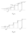
- FIG. 3 shows the generated input measurement signal ES as sample-and-hold element input signal and the sample-and-hold element output signal MS, which is generated as a function thereof.
- FIG. 3a is the input measurement signal ES with the resulting NF envelope H NF and in FIG. 3b shown without enveloping curve.
- the output signal MS of the sample-and-hold device assumes dependent values from the burst pulse of the input measurement signal ES.
- the output signal MS approaches the amplitude of the burst pulse with an exponential profile.
- the capacitor voltage determining the output signal MS during the first period ie during the sampling time, only slightly approaches the value of the incoming burst. Pulse on or the capacitor of the sample-hold member is fully charged to the value of the incoming burst.
- the sample-and-hold element can be designed in such a way that the value of the output signal MS does not substantially correspond to the value of the amplitude of the burst pulse until the end of the sampling time.
- a design of the sample-and-hold element is possible such that, at the end of the first period, the value of the output signal MS is slightly below the amplitude of the burst pulse.
- the sample-and-hold circuit output signal MS is kept constant by the signal value memory means, in particular as a capacitor, substantially at a value which the output signal MS respectively has at the end of the sampling time.
- constant holding is to be understood as holding the value in the context of customary holding drifts.
- the output signal MS of the sample-and-hold element can then be filtered on the basis of a bandpass which only allows frequencies in the range of the LF envelope frequency to pass, and represents the measurement signal to be evaluated on the basis of the phase principle.
- the measurement signal can be digitized by an analog-to-digital converter and compared with a reference signal - for determining the distance of the measurement object - with respect to a phase position by means of a signal processing system.
- FIG. 4 shows a receiving circuit 2 according to the invention for an optical-electronic distance measuring device, which is designed to emit a modulated according to the Burstmodulatoionsong measuring radiation.
- the receiving circuit 2 has a receiver 5 for transforming at least a part of the signals reflected on a measuring object and modulated according to the burst modulation principle Measuring radiation 23 in an electrical input measurement signal ES on.
- a receiver 5 for transforming at least a part of the signals reflected on a measuring object and modulated according to the burst modulation principle Measuring radiation 23 in an electrical input measurement signal ES on.
- an avalanche photodiode APD
- a modulated bias voltage as a mixer voltage
- the receiving circuit has corresponding means 6 for applying the modulated mixer voltage.
- the mixer voltage can be modulated in such a way that the APD current generated as a function of the received measurement radiation essentially has burst pulses of constant width, determined by the active burst time, and modulated amplitude as the input measurement signal ES, and accordingly FIG. 2 - A curve enveloping the burst pulses as a NF envelope H NF substantially sinusoidally with a low-frequency LF envelope frequency.
- the generated APD current as input measurement signal ES now also has frequency components in the region of the modulation frequency, which is connected by a low-pass filter acting as a transimpedance amplifier 7, which is connected between the receiver and the sample-and-hold member 10 and the APD current in an output voltage converts, can be filtered out.
- the output voltage of the transimpedance amplifier 7, which represents the filtered APD input measurement signal ES, is converted by a sample-and-hold element 10 into a sample-and-hold circuit output voltage as a measurement signal MS, wherein the output voltage of the transimpedance amplifier can be considered as sample and hold input voltage.
- the sample-and-hold element 10 may comprise an electronic switch 12 for determining the sample and hold time, a capacitor 11 for holding a voltage value during the hold time, and a charging resistor 13 inter alia for designing the bandwidth of the sample-and-hold element 10. the eg affecting the response time.
- the voltage applied to the capacitor 11 is the sample-and-hold circuit output voltage which represents the measurement signal MS to be evaluated for determining a distance to the measurement object.
- the sampling time of the sample-and-hold element 10 is linked to the active burst time and the hold time to the dead time of the received measurement radiation 23.
- the sampling time can be set equal to the active burst time and the holding time equal to the dead time.
- the switch 12 is then closed during the active burst time so that the capacitor voltage is changed by the incoming burst pulse, respectively, and open during the dead time. During the dead time, therefore, the capacitor voltage is kept substantially constant at that voltage value which occurs at the time the switch 12 is opened.
- the hold time can also be selected slightly longer than the dead time and the sampling time correspondingly shorter than the active burst time, so that the hold time overlaps each slightly with the preceding and / or the subsequent active burst time of the received measurement radiation.
- the input measurement signal ES is therefore not sampled in this variant during the entire active burst time.
- the sampling time can be selected, for example, as 0.8 times the active burst time and accordingly the hold time as 1.05 times the dead time, in which case the holding time with the preceding and following active burst time slightly overlapped.
- the response time of the sample-and-hold element 10 can be selected to be approximately equal to or slightly longer than the sampling time.
- the capacitor 11 is then fully charged or discharged only at the end of the sampling time to a value of the incoming burst, so that the capacitor voltage at the end of the sampling corresponds approximately to the sample-and-hold element input voltage.
- the capacitor 11 is not fully charged or discharged to the value of the incoming bursts, respectively.
- sample-and-hold element 10 is followed by a bandpass filter 8, in particular an antialiasing filter, with pass frequencies only in the vicinity of the LF envelope frequency, so that the sample-and-hold element output signal present as the measurement signal MS is smoothed.
- a bandpass filter 8 in particular an antialiasing filter
- the bandpass filtered measurement signal gMS can now be digitized by an analog-to-digital converter 9. Subsequently, an evaluation of the measurement signal, for example, by a corresponding signal processing software for determining the distance of the measurement object done.
- the noise voltage appearing on the capacitor 11 of the sample and hold element 10 can be considered as follows: During the active burst time T Burst-on , the switch 12 is closed and the noise is in the form of the low-pass filtered input smoke. After the switch 12 has been opened, the voltage remains at the last value of the active burst time. During the hold time, therefore, there is a constant pulse as noise. The height of this pulse is a random process with an expected value of zero.
- the bandpass filter ahead of the analog-to-digital converter 9 allows only the frequencies to pass around the LF envelope frequency, the noise power density of the process occurring during the hold time is only of interest in the vicinity of the LF envelope frequency.
- a specification or optimization of the receiving circuit 2 for example an optimal choice of the bandwidth of the sample-and-hold element 10, can be carried out by a person skilled in the art, depending on the requirements of the distance measuring device incorporating the receiving circuit 2.
- FIG. 5 shows a further embodiment of the inventive receiving circuit 2.
- the in FIG. 5 shown receiving circuit connected to the high-frequency transimpedance amplifier 7 frequency synthesizer for modulating the burst pulse amplitudes of the input measurement signal (ES).
- FIG. 6 shows an optical-electronic distance measuring device 1 according to the invention with a transmitter 3 for emission according to the burst modulation principle - with a burst period of an active burst time and a dead time - modulated optical measuring radiation 21 in the direction of a measuring object 33. Furthermore, the distance measuring device 1, the FIG. 4 illustrated receiving circuit 2 and a signal processing system 4 for determining a distance by evaluating the measurement signal based on reference signals according to the phase measurement principle.
- the laser source as the transmitter 3 emits burst-modulated optical measuring radiation 21 in the direction of a measuring object 33, the distance of which is to be measured by the distance measuring device 1.
- a beam splitter By a beam splitter, a small proportion of the measuring radiation is branched off as reference radiation 22. At least a part of the measuring radiation 23 reflected at the measuring object is collected by a receiving optical system and directed to the receiver 5, which as described above is at a modulated mixer voltage.
- the reference radiation 22 is conducted via a deflecting mirror to a reference receiver 32. The traversed by the reference radiation 22 distance from the beam splitter to the reference receiver 32 forms the known reference distance.
- the burst modulation of the optical measuring radiation is effected, for example, by a modulation signal applied to the transmitter 3, e.g. can be generated by a frequency synthesizer 31.
- the input measurement signal generated by the receiver 5 as an image of the received measuring radiation 23 is transmitted through the receiving circuit 2 as in the description FIG. 4 explained - converted into a measurement signal and then digitized.
- the receiving circuit 2 has means 6 for, in particular, continuous application of a modulated mixer voltage at the receiver 5, the receiver 5 itself, an impedance amplifier 7, according to the invention the sample-and-hold element 10, a bandpass filter 8 with pass frequencies in the range around the LF envelope frequency and a Analog-to-digital converter 9 on.
- the signal processing system 4 now evaluates the digitized measurement signal on the basis of a reference signal generated by the reference receiver 32 and determines therefrom the searched distance of the measurement object.
- the inventive distance measuring device 1 can be designed in particular as a handheld device.
- the modulation signal applied to the transmitter 3 can be provided directly to the signal processing system 4 as a reference signal, so that the measurement signal generated according to the invention is evaluated on the basis of this reference signal and the sought distance of the measurement object is determined therefrom.
- sample-and-hold member according to further known from the prior art embodiments, such as integrated into the analog-to-digital converter, be formed.
- a receiving circuit according to the invention with a sample-and-hold element can also be provided for the reference receiver.
Applications Claiming Priority (2)
| Application Number | Priority Date | Filing Date | Title |
|---|---|---|---|
| CH1912008 | 2008-02-11 | ||
| PCT/EP2009/051191 WO2009101002A1 (de) | 2008-02-11 | 2009-02-03 | Optisch-elektronische entfernungsmessvorrichtung |
Publications (2)
| Publication Number | Publication Date |
|---|---|
| EP2240797A1 EP2240797A1 (de) | 2010-10-20 |
| EP2240797B1 true EP2240797B1 (de) | 2013-05-22 |
Family
ID=39585311
Family Applications (1)
| Application Number | Title | Priority Date | Filing Date |
|---|---|---|---|
| EP09711373.2A Not-in-force EP2240797B1 (de) | 2008-02-11 | 2009-02-03 | Optisch-elektronische entfernungsmessvorrichtung |
Country Status (6)
| Country | Link |
|---|---|
| US (1) | US8279421B2 (zh) |
| EP (1) | EP2240797B1 (zh) |
| CN (1) | CN101946189B (zh) |
| AU (1) | AU2009214252B2 (zh) |
| CA (1) | CA2713652C (zh) |
| WO (1) | WO2009101002A1 (zh) |
Families Citing this family (22)
| Publication number | Priority date | Publication date | Assignee | Title |
|---|---|---|---|---|
| US7146176B2 (en) | 2000-06-13 | 2006-12-05 | Shared Spectrum Company | System and method for reuse of communications spectrum for fixed and mobile applications with efficient method to mitigate interference |
| US7409010B2 (en) | 2003-06-10 | 2008-08-05 | Shared Spectrum Company | Method and system for transmitting signals with reduced spurious emissions |
| US8184653B2 (en) | 2007-08-15 | 2012-05-22 | Shared Spectrum Company | Systems and methods for a cognitive radio having adaptable characteristics |
| US8055204B2 (en) | 2007-08-15 | 2011-11-08 | Shared Spectrum Company | Methods for detecting and classifying signals transmitted over a radio frequency spectrum |
| US8997170B2 (en) | 2006-12-29 | 2015-03-31 | Shared Spectrum Company | Method and device for policy-based control of radio |
| US7564816B2 (en) | 2006-05-12 | 2009-07-21 | Shared Spectrum Company | Method and system for determining spectrum availability within a network |
| US8027249B2 (en) * | 2006-10-18 | 2011-09-27 | Shared Spectrum Company | Methods for using a detector to monitor and detect channel occupancy |
| US8155649B2 (en) | 2006-05-12 | 2012-04-10 | Shared Spectrum Company | Method and system for classifying communication signals in a dynamic spectrum access system |
| US8326313B2 (en) | 2006-05-12 | 2012-12-04 | Shared Spectrum Company | Method and system for dynamic spectrum access using detection periods |
| US9538388B2 (en) | 2006-05-12 | 2017-01-03 | Shared Spectrum Company | Method and system for dynamic spectrum access |
| EP2319260A2 (en) | 2008-08-19 | 2011-05-11 | Shared Spectrum Company | Method and system for dynamic spectrum access using specialty detectors and improved networking |
| US8688045B2 (en) * | 2008-11-19 | 2014-04-01 | Qualcomm Incorporated | FM transmitter and non-FM receiver integrated on single chip |
| US9606228B1 (en) | 2014-02-20 | 2017-03-28 | Banner Engineering Corporation | High-precision digital time-of-flight measurement with coarse delay elements |
| DE102014106463A1 (de) * | 2014-05-08 | 2015-11-12 | Sick Ag | Entfernungsmessender Sensor und Verfahren zur Erfassung und Abstandsbestimmung von Objekten |
| EP3070494B1 (de) * | 2015-03-18 | 2021-04-28 | Leica Geosystems AG | Elektrooptisches distanzmessverfahren und ebensolcher distanzmesser |
| CN105467376B (zh) * | 2016-01-14 | 2019-02-12 | 中国人民解放军空军工程大学 | 大调谐范围线性调频信号产生方法及其装置 |
| MX2017003334A (es) * | 2017-03-14 | 2018-09-13 | Albert Remberg Bueno Ernst | Medidor electrooptico integral para la medicion de distancias de uso automotriz. |
| US10353058B2 (en) * | 2017-10-06 | 2019-07-16 | Osram Opto Semiconductors Gmbh | Signal processing unit and method for time of flight measurement |
| CN108761473A (zh) * | 2018-03-29 | 2018-11-06 | 广东美的制冷设备有限公司 | 空调器的房间大小检测方法、空调器和计算机存储介质 |
| WO2020042166A1 (zh) * | 2018-08-31 | 2020-03-05 | 深圳市汇顶科技股份有限公司 | 基于飞行时间的测距方法和测距系统 |
| CN111736014B (zh) * | 2020-07-20 | 2020-11-24 | 中国空气动力研究与发展中心低速空气动力研究所 | 一种频率信号采集和数据处理方法及装置 |
| CN112526536B (zh) * | 2020-11-25 | 2023-09-22 | 中国人民解放军陆军工程大学 | 一种基于脉冲串技术的单光子测距系统及方法 |
Family Cites Families (4)
| Publication number | Priority date | Publication date | Assignee | Title |
|---|---|---|---|---|
| DE4316348A1 (de) * | 1993-05-15 | 1994-11-17 | Wild Heerbrugg Ag | Vorrichtung zur Distanzmessung |
| WO2002016964A1 (de) | 2000-08-25 | 2002-02-28 | Kurt Giger | Verfahren und vorrichtung zur entfernungsmessung |
| WO2005008271A2 (en) * | 2002-11-26 | 2005-01-27 | Munro James F | An apparatus for high accuracy distance and velocity measurement and methods thereof |
| US7379016B1 (en) * | 2006-02-16 | 2008-05-27 | Mcewan Technologies, Llc | Carrier phase detection system for radar sensors |
-
2009
- 2009-02-03 AU AU2009214252A patent/AU2009214252B2/en not_active Ceased
- 2009-02-03 EP EP09711373.2A patent/EP2240797B1/de not_active Not-in-force
- 2009-02-03 CN CN2009801047676A patent/CN101946189B/zh not_active Expired - Fee Related
- 2009-02-03 CA CA2713652A patent/CA2713652C/en not_active Expired - Fee Related
- 2009-02-03 WO PCT/EP2009/051191 patent/WO2009101002A1/de active Application Filing
- 2009-02-03 US US12/812,628 patent/US8279421B2/en active Active
Also Published As
| Publication number | Publication date |
|---|---|
| CN101946189A (zh) | 2011-01-12 |
| CA2713652C (en) | 2014-04-29 |
| US8279421B2 (en) | 2012-10-02 |
| EP2240797A1 (de) | 2010-10-20 |
| AU2009214252A1 (en) | 2009-08-20 |
| AU2009214252B2 (en) | 2012-05-24 |
| WO2009101002A1 (de) | 2009-08-20 |
| CN101946189B (zh) | 2013-10-16 |
| CA2713652A1 (en) | 2009-08-20 |
| US20100296078A1 (en) | 2010-11-25 |
Similar Documents
| Publication | Publication Date | Title |
|---|---|---|
| EP2240797B1 (de) | Optisch-elektronische entfernungsmessvorrichtung | |
| EP1311873B1 (de) | Verfahren und vorrichtung zur entfernungsmessung | |
| AT412023B (de) | Verfahren und einrichtung zur elektrooptischen distanzmessung | |
| EP1320766B1 (de) | Vorrichtung und verfahren zur signalerfassung bei einem entfernungsmessgerät | |
| DE102005045993B4 (de) | Verfahren zur Lichtlaufzeitmessung | |
| DE3034511C2 (de) | Hindernisdetektor für Fahrzeuge | |
| EP1423731B1 (de) | Verfahren und vorrichtung zur aufnahme eines dreidimensionalen abstandsbildes | |
| EP2637038B1 (de) | Entfernungsmesser | |
| EP1529194B1 (de) | Verfahren und vorrichtung zur optischen distanzmessung | |
| DE102011056963C5 (de) | Messung von Entfernungen nach dem Signallaufzeitprinzip | |
| EP2126607B1 (de) | Umfeldsensor zur detektion von objekten und betriebsverfahren hierfür | |
| EP2002208A1 (de) | Vorrichtung zur optischen distanzmessung sowie verfahren zum betrieb einer solchen vorrichtung | |
| DE10130763A1 (de) | Vorrichtung zur optischen Distanzmessung über einen grossen Messbereich | |
| DE102014013099A1 (de) | Verfahren und Vorrichtung zur vereinfachten Erfassung eines Tiefenbildes | |
| WO2020114769A2 (de) | Verfahren zum bestimmen des abstands und rückstrahlvermögens einer objektoberfläche | |
| EP2182379B1 (de) | Entfernungsmessender Laserscanner | |
| EP1585234B1 (de) | Photomischdetektor (PMD)-System und Verfahren zum Betreiben desselben | |
| DE102017106226A1 (de) | LIDAR-Messeinrichtung | |
| DE102019207741A1 (de) | Ein LIDAR-System, ein Verfahren für ein LIDAR-System und ein Empfänger für ein LIDAR-System mit ersten und zweiten Umwandlungselementen | |
| DE102015225192A1 (de) | Lichtlaufzeitmesssystem mit Überreichweitenerkennung | |
| EP3654056A1 (de) | Sensor und verfahren zur erfassung von objekten | |
| EP4249949B1 (de) | Erfassung und abstandsbestimmung eines objekts | |
| EP4184201B1 (de) | Optoelektronischer sensor und verfahren zum ausrichten eines optoelektronischen sensors | |
| EP4249950B1 (de) | Erfassung und abstandsbestimmung eines objekts | |
| DE3335869A1 (de) | Optische radarvorrichtung fuer fahrzeuge |
Legal Events
| Date | Code | Title | Description |
|---|---|---|---|
| PUAI | Public reference made under article 153(3) epc to a published international application that has entered the european phase |
Free format text: ORIGINAL CODE: 0009012 |
|
| 17P | Request for examination filed |
Effective date: 20100618 |
|
| AK | Designated contracting states |
Kind code of ref document: A1 Designated state(s): AT BE BG CH CY CZ DE DK EE ES FI FR GB GR HR HU IE IS IT LI LT LU LV MC MK MT NL NO PL PT RO SE SI SK TR |
|
| AX | Request for extension of the european patent |
Extension state: AL BA RS |
|
| RIN1 | Information on inventor provided before grant (corrected) |
Inventor name: GIGER, KURT Inventor name: FORRER, PETER |
|
| DAX | Request for extension of the european patent (deleted) | ||
| GRAP | Despatch of communication of intention to grant a patent |
Free format text: ORIGINAL CODE: EPIDOSNIGR1 |
|
| GRAS | Grant fee paid |
Free format text: ORIGINAL CODE: EPIDOSNIGR3 |
|
| GRAA | (expected) grant |
Free format text: ORIGINAL CODE: 0009210 |
|
| AK | Designated contracting states |
Kind code of ref document: B1 Designated state(s): AT BE BG CH CY CZ DE DK EE ES FI FR GB GR HR HU IE IS IT LI LT LU LV MC MK MT NL NO PL PT RO SE SI SK TR |
|
| REG | Reference to a national code |
Ref country code: GB Ref legal event code: FG4D Free format text: NOT ENGLISH |
|
| REG | Reference to a national code |
Ref country code: CH Ref legal event code: EP |
|
| REG | Reference to a national code |
Ref country code: CH Ref legal event code: NV Representative=s name: KAMINSKI HARMANN PATENTANWAELTE EST., LI |
|
| REG | Reference to a national code |
Ref country code: AT Ref legal event code: REF Ref document number: 613506 Country of ref document: AT Kind code of ref document: T Effective date: 20130615 |
|
| REG | Reference to a national code |
Ref country code: IE Ref legal event code: FG4D Free format text: LANGUAGE OF EP DOCUMENT: GERMAN |
|
| REG | Reference to a national code |
Ref country code: DE Ref legal event code: R096 Ref document number: 502009007155 Country of ref document: DE Effective date: 20130718 |
|
| REG | Reference to a national code |
Ref country code: SE Ref legal event code: TRGR |
|
| REG | Reference to a national code |
Ref country code: NL Ref legal event code: T3 |
|
| REG | Reference to a national code |
Ref country code: LT Ref legal event code: MG4D |
|
| PG25 | Lapsed in a contracting state [announced via postgrant information from national office to epo] |
Ref country code: SI Free format text: LAPSE BECAUSE OF FAILURE TO SUBMIT A TRANSLATION OF THE DESCRIPTION OR TO PAY THE FEE WITHIN THE PRESCRIBED TIME-LIMIT Effective date: 20130522 Ref country code: FI Free format text: LAPSE BECAUSE OF FAILURE TO SUBMIT A TRANSLATION OF THE DESCRIPTION OR TO PAY THE FEE WITHIN THE PRESCRIBED TIME-LIMIT Effective date: 20130522 Ref country code: GR Free format text: LAPSE BECAUSE OF FAILURE TO SUBMIT A TRANSLATION OF THE DESCRIPTION OR TO PAY THE FEE WITHIN THE PRESCRIBED TIME-LIMIT Effective date: 20130823 Ref country code: IS Free format text: LAPSE BECAUSE OF FAILURE TO SUBMIT A TRANSLATION OF THE DESCRIPTION OR TO PAY THE FEE WITHIN THE PRESCRIBED TIME-LIMIT Effective date: 20130922 Ref country code: PT Free format text: LAPSE BECAUSE OF FAILURE TO SUBMIT A TRANSLATION OF THE DESCRIPTION OR TO PAY THE FEE WITHIN THE PRESCRIBED TIME-LIMIT Effective date: 20130923 Ref country code: ES Free format text: LAPSE BECAUSE OF FAILURE TO SUBMIT A TRANSLATION OF THE DESCRIPTION OR TO PAY THE FEE WITHIN THE PRESCRIBED TIME-LIMIT Effective date: 20130902 Ref country code: NO Free format text: LAPSE BECAUSE OF FAILURE TO SUBMIT A TRANSLATION OF THE DESCRIPTION OR TO PAY THE FEE WITHIN THE PRESCRIBED TIME-LIMIT Effective date: 20130822 Ref country code: LT Free format text: LAPSE BECAUSE OF FAILURE TO SUBMIT A TRANSLATION OF THE DESCRIPTION OR TO PAY THE FEE WITHIN THE PRESCRIBED TIME-LIMIT Effective date: 20130522 |
|
| PG25 | Lapsed in a contracting state [announced via postgrant information from national office to epo] |
Ref country code: BG Free format text: LAPSE BECAUSE OF FAILURE TO SUBMIT A TRANSLATION OF THE DESCRIPTION OR TO PAY THE FEE WITHIN THE PRESCRIBED TIME-LIMIT Effective date: 20130822 Ref country code: PL Free format text: LAPSE BECAUSE OF FAILURE TO SUBMIT A TRANSLATION OF THE DESCRIPTION OR TO PAY THE FEE WITHIN THE PRESCRIBED TIME-LIMIT Effective date: 20130522 Ref country code: HR Free format text: LAPSE BECAUSE OF FAILURE TO SUBMIT A TRANSLATION OF THE DESCRIPTION OR TO PAY THE FEE WITHIN THE PRESCRIBED TIME-LIMIT Effective date: 20130522 |
|
| PG25 | Lapsed in a contracting state [announced via postgrant information from national office to epo] |
Ref country code: LV Free format text: LAPSE BECAUSE OF FAILURE TO SUBMIT A TRANSLATION OF THE DESCRIPTION OR TO PAY THE FEE WITHIN THE PRESCRIBED TIME-LIMIT Effective date: 20130522 |
|
| PG25 | Lapsed in a contracting state [announced via postgrant information from national office to epo] |
Ref country code: CZ Free format text: LAPSE BECAUSE OF FAILURE TO SUBMIT A TRANSLATION OF THE DESCRIPTION OR TO PAY THE FEE WITHIN THE PRESCRIBED TIME-LIMIT Effective date: 20130522 Ref country code: EE Free format text: LAPSE BECAUSE OF FAILURE TO SUBMIT A TRANSLATION OF THE DESCRIPTION OR TO PAY THE FEE WITHIN THE PRESCRIBED TIME-LIMIT Effective date: 20130522 Ref country code: SK Free format text: LAPSE BECAUSE OF FAILURE TO SUBMIT A TRANSLATION OF THE DESCRIPTION OR TO PAY THE FEE WITHIN THE PRESCRIBED TIME-LIMIT Effective date: 20130522 Ref country code: DK Free format text: LAPSE BECAUSE OF FAILURE TO SUBMIT A TRANSLATION OF THE DESCRIPTION OR TO PAY THE FEE WITHIN THE PRESCRIBED TIME-LIMIT Effective date: 20130522 |
|
| PG25 | Lapsed in a contracting state [announced via postgrant information from national office to epo] |
Ref country code: RO Free format text: LAPSE BECAUSE OF FAILURE TO SUBMIT A TRANSLATION OF THE DESCRIPTION OR TO PAY THE FEE WITHIN THE PRESCRIBED TIME-LIMIT Effective date: 20130522 Ref country code: IT Free format text: LAPSE BECAUSE OF FAILURE TO SUBMIT A TRANSLATION OF THE DESCRIPTION OR TO PAY THE FEE WITHIN THE PRESCRIBED TIME-LIMIT Effective date: 20130522 |
|
| PLBE | No opposition filed within time limit |
Free format text: ORIGINAL CODE: 0009261 |
|
| STAA | Information on the status of an ep patent application or granted ep patent |
Free format text: STATUS: NO OPPOSITION FILED WITHIN TIME LIMIT |
|
| 26N | No opposition filed |
Effective date: 20140225 |
|
| REG | Reference to a national code |
Ref country code: DE Ref legal event code: R097 Ref document number: 502009007155 Country of ref document: DE Effective date: 20140225 |
|
| BERE | Be: lapsed |
Owner name: LEICA GEOSYSTEMS A.G. Effective date: 20140228 |
|
| PG25 | Lapsed in a contracting state [announced via postgrant information from national office to epo] |
Ref country code: LU Free format text: LAPSE BECAUSE OF FAILURE TO SUBMIT A TRANSLATION OF THE DESCRIPTION OR TO PAY THE FEE WITHIN THE PRESCRIBED TIME-LIMIT Effective date: 20140203 Ref country code: MC Free format text: LAPSE BECAUSE OF FAILURE TO SUBMIT A TRANSLATION OF THE DESCRIPTION OR TO PAY THE FEE WITHIN THE PRESCRIBED TIME-LIMIT Effective date: 20130522 |
|
| REG | Reference to a national code |
Ref country code: IE Ref legal event code: MM4A |
|
| PG25 | Lapsed in a contracting state [announced via postgrant information from national office to epo] |
Ref country code: IE Free format text: LAPSE BECAUSE OF NON-PAYMENT OF DUE FEES Effective date: 20140203 Ref country code: BE Free format text: LAPSE BECAUSE OF NON-PAYMENT OF DUE FEES Effective date: 20140228 |
|
| REG | Reference to a national code |
Ref country code: AT Ref legal event code: MM01 Ref document number: 613506 Country of ref document: AT Kind code of ref document: T Effective date: 20140203 |
|
| PG25 | Lapsed in a contracting state [announced via postgrant information from national office to epo] |
Ref country code: AT Free format text: LAPSE BECAUSE OF NON-PAYMENT OF DUE FEES Effective date: 20140203 |
|
| REG | Reference to a national code |
Ref country code: FR Ref legal event code: PLFP Year of fee payment: 8 |
|
| PG25 | Lapsed in a contracting state [announced via postgrant information from national office to epo] |
Ref country code: MT Free format text: LAPSE BECAUSE OF FAILURE TO SUBMIT A TRANSLATION OF THE DESCRIPTION OR TO PAY THE FEE WITHIN THE PRESCRIBED TIME-LIMIT Effective date: 20130522 |
|
| PG25 | Lapsed in a contracting state [announced via postgrant information from national office to epo] |
Ref country code: CY Free format text: LAPSE BECAUSE OF FAILURE TO SUBMIT A TRANSLATION OF THE DESCRIPTION OR TO PAY THE FEE WITHIN THE PRESCRIBED TIME-LIMIT Effective date: 20130522 |
|
| PG25 | Lapsed in a contracting state [announced via postgrant information from national office to epo] |
Ref country code: HU Free format text: LAPSE BECAUSE OF FAILURE TO SUBMIT A TRANSLATION OF THE DESCRIPTION OR TO PAY THE FEE WITHIN THE PRESCRIBED TIME-LIMIT; INVALID AB INITIO Effective date: 20090203 Ref country code: TR Free format text: LAPSE BECAUSE OF FAILURE TO SUBMIT A TRANSLATION OF THE DESCRIPTION OR TO PAY THE FEE WITHIN THE PRESCRIBED TIME-LIMIT Effective date: 20130522 |
|
| REG | Reference to a national code |
Ref country code: FR Ref legal event code: PLFP Year of fee payment: 9 |
|
| REG | Reference to a national code |
Ref country code: FR Ref legal event code: PLFP Year of fee payment: 10 |
|
| PG25 | Lapsed in a contracting state [announced via postgrant information from national office to epo] |
Ref country code: MK Free format text: LAPSE BECAUSE OF FAILURE TO SUBMIT A TRANSLATION OF THE DESCRIPTION OR TO PAY THE FEE WITHIN THE PRESCRIBED TIME-LIMIT Effective date: 20130522 |
|
| PGFP | Annual fee paid to national office [announced via postgrant information from national office to epo] |
Ref country code: NL Payment date: 20200219 Year of fee payment: 12 Ref country code: GB Payment date: 20200219 Year of fee payment: 12 Ref country code: SE Payment date: 20200220 Year of fee payment: 12 Ref country code: DE Payment date: 20200219 Year of fee payment: 12 |
|
| PGFP | Annual fee paid to national office [announced via postgrant information from national office to epo] |
Ref country code: CH Payment date: 20200219 Year of fee payment: 12 |
|
| PGFP | Annual fee paid to national office [announced via postgrant information from national office to epo] |
Ref country code: FR Payment date: 20200219 Year of fee payment: 12 |
|
| REG | Reference to a national code |
Ref country code: DE Ref legal event code: R119 Ref document number: 502009007155 Country of ref document: DE |
|
| REG | Reference to a national code |
Ref country code: SE Ref legal event code: EUG |
|
| GBPC | Gb: european patent ceased through non-payment of renewal fee |
Effective date: 20210203 |
|
| PG25 | Lapsed in a contracting state [announced via postgrant information from national office to epo] |
Ref country code: CH Free format text: LAPSE BECAUSE OF NON-PAYMENT OF DUE FEES Effective date: 20210228 Ref country code: LI Free format text: LAPSE BECAUSE OF NON-PAYMENT OF DUE FEES Effective date: 20210228 |
|
| PG25 | Lapsed in a contracting state [announced via postgrant information from national office to epo] |
Ref country code: SE Free format text: LAPSE BECAUSE OF NON-PAYMENT OF DUE FEES Effective date: 20210204 |
|
| REG | Reference to a national code |
Ref country code: NL Ref legal event code: MM Effective date: 20210301 |
|
| PG25 | Lapsed in a contracting state [announced via postgrant information from national office to epo] |
Ref country code: NL Free format text: LAPSE BECAUSE OF NON-PAYMENT OF DUE FEES Effective date: 20210301 |
|
| PG25 | Lapsed in a contracting state [announced via postgrant information from national office to epo] |
Ref country code: GB Free format text: LAPSE BECAUSE OF NON-PAYMENT OF DUE FEES Effective date: 20210203 Ref country code: FR Free format text: LAPSE BECAUSE OF NON-PAYMENT OF DUE FEES Effective date: 20210228 Ref country code: DE Free format text: LAPSE BECAUSE OF NON-PAYMENT OF DUE FEES Effective date: 20210901 |