EP2239630A2 - Method for selective adsorption of noble metal catalyst onto surface of polymer - Google Patents
Method for selective adsorption of noble metal catalyst onto surface of polymer Download PDFInfo
- Publication number
- EP2239630A2 EP2239630A2 EP09706192A EP09706192A EP2239630A2 EP 2239630 A2 EP2239630 A2 EP 2239630A2 EP 09706192 A EP09706192 A EP 09706192A EP 09706192 A EP09706192 A EP 09706192A EP 2239630 A2 EP2239630 A2 EP 2239630A2
- Authority
- EP
- European Patent Office
- Prior art keywords
- polymer
- metal catalyst
- photosensitive
- precious metal
- ions
- Prior art date
- Legal status (The legal status is an assumption and is not a legal conclusion. Google has not performed a legal analysis and makes no representation as to the accuracy of the status listed.)
- Withdrawn
Links
Images


Classifications
-
- G—PHYSICS
- G03—PHOTOGRAPHY; CINEMATOGRAPHY; ANALOGOUS TECHNIQUES USING WAVES OTHER THAN OPTICAL WAVES; ELECTROGRAPHY; HOLOGRAPHY
- G03F—PHOTOMECHANICAL PRODUCTION OF TEXTURED OR PATTERNED SURFACES, e.g. FOR PRINTING, FOR PROCESSING OF SEMICONDUCTOR DEVICES; MATERIALS THEREFOR; ORIGINALS THEREFOR; APPARATUS SPECIALLY ADAPTED THEREFOR
- G03F7/00—Photomechanical, e.g. photolithographic, production of textured or patterned surfaces, e.g. printing surfaces; Materials therefor, e.g. comprising photoresists; Apparatus specially adapted therefor
- G03F7/004—Photosensitive materials
- G03F7/0042—Photosensitive materials with inorganic or organometallic light-sensitive compounds not otherwise provided for, e.g. inorganic resists
-
- C—CHEMISTRY; METALLURGY
- C23—COATING METALLIC MATERIAL; COATING MATERIAL WITH METALLIC MATERIAL; CHEMICAL SURFACE TREATMENT; DIFFUSION TREATMENT OF METALLIC MATERIAL; COATING BY VACUUM EVAPORATION, BY SPUTTERING, BY ION IMPLANTATION OR BY CHEMICAL VAPOUR DEPOSITION, IN GENERAL; INHIBITING CORROSION OF METALLIC MATERIAL OR INCRUSTATION IN GENERAL
- C23C—COATING METALLIC MATERIAL; COATING MATERIAL WITH METALLIC MATERIAL; SURFACE TREATMENT OF METALLIC MATERIAL BY DIFFUSION INTO THE SURFACE, BY CHEMICAL CONVERSION OR SUBSTITUTION; COATING BY VACUUM EVAPORATION, BY SPUTTERING, BY ION IMPLANTATION OR BY CHEMICAL VAPOUR DEPOSITION, IN GENERAL
- C23C18/00—Chemical coating by decomposition of either liquid compounds or solutions of the coating forming compounds, without leaving reaction products of surface material in the coating; Contact plating
- C23C18/16—Chemical coating by decomposition of either liquid compounds or solutions of the coating forming compounds, without leaving reaction products of surface material in the coating; Contact plating by reduction or substitution, e.g. electroless plating
- C23C18/1601—Process or apparatus
- C23C18/1603—Process or apparatus coating on selected surface areas
- C23C18/1605—Process or apparatus coating on selected surface areas by masking
-
- C—CHEMISTRY; METALLURGY
- C23—COATING METALLIC MATERIAL; COATING MATERIAL WITH METALLIC MATERIAL; CHEMICAL SURFACE TREATMENT; DIFFUSION TREATMENT OF METALLIC MATERIAL; COATING BY VACUUM EVAPORATION, BY SPUTTERING, BY ION IMPLANTATION OR BY CHEMICAL VAPOUR DEPOSITION, IN GENERAL; INHIBITING CORROSION OF METALLIC MATERIAL OR INCRUSTATION IN GENERAL
- C23C—COATING METALLIC MATERIAL; COATING MATERIAL WITH METALLIC MATERIAL; SURFACE TREATMENT OF METALLIC MATERIAL BY DIFFUSION INTO THE SURFACE, BY CHEMICAL CONVERSION OR SUBSTITUTION; COATING BY VACUUM EVAPORATION, BY SPUTTERING, BY ION IMPLANTATION OR BY CHEMICAL VAPOUR DEPOSITION, IN GENERAL
- C23C18/00—Chemical coating by decomposition of either liquid compounds or solutions of the coating forming compounds, without leaving reaction products of surface material in the coating; Contact plating
- C23C18/16—Chemical coating by decomposition of either liquid compounds or solutions of the coating forming compounds, without leaving reaction products of surface material in the coating; Contact plating by reduction or substitution, e.g. electroless plating
- C23C18/1601—Process or apparatus
- C23C18/1603—Process or apparatus coating on selected surface areas
- C23C18/1607—Process or apparatus coating on selected surface areas by direct patterning
- C23C18/1608—Process or apparatus coating on selected surface areas by direct patterning from pretreatment step, i.e. selective pre-treatment
-
- C—CHEMISTRY; METALLURGY
- C23—COATING METALLIC MATERIAL; COATING MATERIAL WITH METALLIC MATERIAL; CHEMICAL SURFACE TREATMENT; DIFFUSION TREATMENT OF METALLIC MATERIAL; COATING BY VACUUM EVAPORATION, BY SPUTTERING, BY ION IMPLANTATION OR BY CHEMICAL VAPOUR DEPOSITION, IN GENERAL; INHIBITING CORROSION OF METALLIC MATERIAL OR INCRUSTATION IN GENERAL
- C23C—COATING METALLIC MATERIAL; COATING MATERIAL WITH METALLIC MATERIAL; SURFACE TREATMENT OF METALLIC MATERIAL BY DIFFUSION INTO THE SURFACE, BY CHEMICAL CONVERSION OR SUBSTITUTION; COATING BY VACUUM EVAPORATION, BY SPUTTERING, BY ION IMPLANTATION OR BY CHEMICAL VAPOUR DEPOSITION, IN GENERAL
- C23C18/00—Chemical coating by decomposition of either liquid compounds or solutions of the coating forming compounds, without leaving reaction products of surface material in the coating; Contact plating
- C23C18/16—Chemical coating by decomposition of either liquid compounds or solutions of the coating forming compounds, without leaving reaction products of surface material in the coating; Contact plating by reduction or substitution, e.g. electroless plating
- C23C18/1601—Process or apparatus
- C23C18/1603—Process or apparatus coating on selected surface areas
- C23C18/1607—Process or apparatus coating on selected surface areas by direct patterning
- C23C18/1612—Process or apparatus coating on selected surface areas by direct patterning through irradiation means
-
- C—CHEMISTRY; METALLURGY
- C23—COATING METALLIC MATERIAL; COATING MATERIAL WITH METALLIC MATERIAL; CHEMICAL SURFACE TREATMENT; DIFFUSION TREATMENT OF METALLIC MATERIAL; COATING BY VACUUM EVAPORATION, BY SPUTTERING, BY ION IMPLANTATION OR BY CHEMICAL VAPOUR DEPOSITION, IN GENERAL; INHIBITING CORROSION OF METALLIC MATERIAL OR INCRUSTATION IN GENERAL
- C23C—COATING METALLIC MATERIAL; COATING MATERIAL WITH METALLIC MATERIAL; SURFACE TREATMENT OF METALLIC MATERIAL BY DIFFUSION INTO THE SURFACE, BY CHEMICAL CONVERSION OR SUBSTITUTION; COATING BY VACUUM EVAPORATION, BY SPUTTERING, BY ION IMPLANTATION OR BY CHEMICAL VAPOUR DEPOSITION, IN GENERAL
- C23C18/00—Chemical coating by decomposition of either liquid compounds or solutions of the coating forming compounds, without leaving reaction products of surface material in the coating; Contact plating
- C23C18/16—Chemical coating by decomposition of either liquid compounds or solutions of the coating forming compounds, without leaving reaction products of surface material in the coating; Contact plating by reduction or substitution, e.g. electroless plating
- C23C18/18—Pretreatment of the material to be coated
- C23C18/20—Pretreatment of the material to be coated of organic surfaces, e.g. resins
- C23C18/2006—Pretreatment of the material to be coated of organic surfaces, e.g. resins by other methods than those of C23C18/22 - C23C18/30
- C23C18/2046—Pretreatment of the material to be coated of organic surfaces, e.g. resins by other methods than those of C23C18/22 - C23C18/30 by chemical pretreatment
- C23C18/2073—Multistep pretreatment
- C23C18/208—Multistep pretreatment with use of metal first
-
- C—CHEMISTRY; METALLURGY
- C23—COATING METALLIC MATERIAL; COATING MATERIAL WITH METALLIC MATERIAL; CHEMICAL SURFACE TREATMENT; DIFFUSION TREATMENT OF METALLIC MATERIAL; COATING BY VACUUM EVAPORATION, BY SPUTTERING, BY ION IMPLANTATION OR BY CHEMICAL VAPOUR DEPOSITION, IN GENERAL; INHIBITING CORROSION OF METALLIC MATERIAL OR INCRUSTATION IN GENERAL
- C23C—COATING METALLIC MATERIAL; COATING MATERIAL WITH METALLIC MATERIAL; SURFACE TREATMENT OF METALLIC MATERIAL BY DIFFUSION INTO THE SURFACE, BY CHEMICAL CONVERSION OR SUBSTITUTION; COATING BY VACUUM EVAPORATION, BY SPUTTERING, BY ION IMPLANTATION OR BY CHEMICAL VAPOUR DEPOSITION, IN GENERAL
- C23C18/00—Chemical coating by decomposition of either liquid compounds or solutions of the coating forming compounds, without leaving reaction products of surface material in the coating; Contact plating
- C23C18/16—Chemical coating by decomposition of either liquid compounds or solutions of the coating forming compounds, without leaving reaction products of surface material in the coating; Contact plating by reduction or substitution, e.g. electroless plating
- C23C18/18—Pretreatment of the material to be coated
- C23C18/20—Pretreatment of the material to be coated of organic surfaces, e.g. resins
- C23C18/28—Sensitising or activating
-
- G—PHYSICS
- G03—PHOTOGRAPHY; CINEMATOGRAPHY; ANALOGOUS TECHNIQUES USING WAVES OTHER THAN OPTICAL WAVES; ELECTROGRAPHY; HOLOGRAPHY
- G03F—PHOTOMECHANICAL PRODUCTION OF TEXTURED OR PATTERNED SURFACES, e.g. FOR PRINTING, FOR PROCESSING OF SEMICONDUCTOR DEVICES; MATERIALS THEREFOR; ORIGINALS THEREFOR; APPARATUS SPECIALLY ADAPTED THEREFOR
- G03F7/00—Photomechanical, e.g. photolithographic, production of textured or patterned surfaces, e.g. printing surfaces; Materials therefor, e.g. comprising photoresists; Apparatus specially adapted therefor
- G03F7/004—Photosensitive materials
- G03F7/0045—Photosensitive materials with organic non-macromolecular light-sensitive compounds not otherwise provided for, e.g. dissolution inhibitors
-
- G—PHYSICS
- G03—PHOTOGRAPHY; CINEMATOGRAPHY; ANALOGOUS TECHNIQUES USING WAVES OTHER THAN OPTICAL WAVES; ELECTROGRAPHY; HOLOGRAPHY
- G03F—PHOTOMECHANICAL PRODUCTION OF TEXTURED OR PATTERNED SURFACES, e.g. FOR PRINTING, FOR PROCESSING OF SEMICONDUCTOR DEVICES; MATERIALS THEREFOR; ORIGINALS THEREFOR; APPARATUS SPECIALLY ADAPTED THEREFOR
- G03F7/00—Photomechanical, e.g. photolithographic, production of textured or patterned surfaces, e.g. printing surfaces; Materials therefor, e.g. comprising photoresists; Apparatus specially adapted therefor
- G03F7/20—Exposure; Apparatus therefor
-
- G—PHYSICS
- G03—PHOTOGRAPHY; CINEMATOGRAPHY; ANALOGOUS TECHNIQUES USING WAVES OTHER THAN OPTICAL WAVES; ELECTROGRAPHY; HOLOGRAPHY
- G03F—PHOTOMECHANICAL PRODUCTION OF TEXTURED OR PATTERNED SURFACES, e.g. FOR PRINTING, FOR PROCESSING OF SEMICONDUCTOR DEVICES; MATERIALS THEREFOR; ORIGINALS THEREFOR; APPARATUS SPECIALLY ADAPTED THEREFOR
- G03F7/00—Photomechanical, e.g. photolithographic, production of textured or patterned surfaces, e.g. printing surfaces; Materials therefor, e.g. comprising photoresists; Apparatus specially adapted therefor
- G03F7/26—Processing photosensitive materials; Apparatus therefor
- G03F7/265—Selective reaction with inorganic or organometallic reagents after image-wise exposure, e.g. silylation
-
- H—ELECTRICITY
- H05—ELECTRIC TECHNIQUES NOT OTHERWISE PROVIDED FOR
- H05K—PRINTED CIRCUITS; CASINGS OR CONSTRUCTIONAL DETAILS OF ELECTRIC APPARATUS; MANUFACTURE OF ASSEMBLAGES OF ELECTRICAL COMPONENTS
- H05K3/00—Apparatus or processes for manufacturing printed circuits
- H05K3/10—Apparatus or processes for manufacturing printed circuits in which conductive material is applied to the insulating support in such a manner as to form the desired conductive pattern
- H05K3/18—Apparatus or processes for manufacturing printed circuits in which conductive material is applied to the insulating support in such a manner as to form the desired conductive pattern using precipitation techniques to apply the conductive material
- H05K3/181—Apparatus or processes for manufacturing printed circuits in which conductive material is applied to the insulating support in such a manner as to form the desired conductive pattern using precipitation techniques to apply the conductive material by electroless plating
- H05K3/182—Apparatus or processes for manufacturing printed circuits in which conductive material is applied to the insulating support in such a manner as to form the desired conductive pattern using precipitation techniques to apply the conductive material by electroless plating characterised by the patterning method
- H05K3/185—Apparatus or processes for manufacturing printed circuits in which conductive material is applied to the insulating support in such a manner as to form the desired conductive pattern using precipitation techniques to apply the conductive material by electroless plating characterised by the patterning method by making a catalytic pattern by photo-imaging
-
- Y—GENERAL TAGGING OF NEW TECHNOLOGICAL DEVELOPMENTS; GENERAL TAGGING OF CROSS-SECTIONAL TECHNOLOGIES SPANNING OVER SEVERAL SECTIONS OF THE IPC; TECHNICAL SUBJECTS COVERED BY FORMER USPC CROSS-REFERENCE ART COLLECTIONS [XRACs] AND DIGESTS
- Y10—TECHNICAL SUBJECTS COVERED BY FORMER USPC
- Y10T—TECHNICAL SUBJECTS COVERED BY FORMER US CLASSIFICATION
- Y10T428/00—Stock material or miscellaneous articles
- Y10T428/24—Structurally defined web or sheet [e.g., overall dimension, etc.]
- Y10T428/24802—Discontinuous or differential coating, impregnation or bond [e.g., artwork, printing, retouched photograph, etc.]
- Y10T428/24917—Discontinuous or differential coating, impregnation or bond [e.g., artwork, printing, retouched photograph, etc.] including metal layer
Definitions
- the present invention relates to a method of selectively adsorbing a precious metal catalyst on polymer surface.
- a polymer film including a metal layer having a predetermined form can be manufactured using the method.
- PI polyimide
- PET polyethylene terephthalate
- a method of forming a metal circuit pattern by forming a predetermined circuit pattern on the surface of a polymer clad or deposited with thin copper foil using photoresist processing and then etching the copper foil is widely used.
- Such a conventional technology used to form a metal circuit pattern is problematic in that it is complicated, it includes long unit processes, it needs high-priced equipment, and it causes environmental pollution due to the formation of a corrosive etching solution. Further, this conventional technology used to form a metal circuit pattern is problematic in that cheap raw materials and expensive precise equipment are additionally required to realize a micro-circuit pattern or it is very difficult to realize the micro-circuit pattern.
- a laminating or casting process methods of forming a metal layer on a polymer material are conducted by a laminating or casting process.
- a polymer material is surface-modified by plasma ions, and then a conductive metal junction layer is formed on the surface of the surface-modified polymer material using a dry surface treatment technology such as sputtering, metal deposition or the like, and then a metal coating layer is formed on the surface of the conductive metal junction layer using an electroplating technology or a copper film is directly bonded to the surface of the polymer material.
- a process of metalizing a polymer film using wet surface treatment has been developed.
- a metal circuit is also formed by forming a metal layer on a polymer material and then etching the metal layer with copper using photoresist processing.
- this process is also problematic in that it is not easy to form a relatively uniform metal layer, and in that high production expenses are incurred.
- the present inventors found that the above problems can be solved by using a method of adsorbing a precious metal catalyst on a polymer film during wet surface treatment. Based on this finding, the present invention was completed.
- An object of the present invention is to provide a method of selectively adsorbing a precious metal catalyst on polymer surface.
- Another object of the present invention is to provide a polymer film including a metal layer formed by wet-plating the polymer on which the precious metal catalyst is selectively adsorbed using the method.
- the polymer adsorbed with the precious metal catalyst, prepared using the method of the present invention is advantageous in that various shapes of metal pattern layers can be simply and easily formed on the surface thereof, and a metal circuit layer made of copper, nickel or the like adheres closely to the surface thereof, and thus it can be easily used in automobiles, electronics, communications and semiconductors requiring micro-circuit boards. Further, when the polymer is prepared using the method of the present invention, there is an advantage in that the manufacturing cost thereof becomes low compared to conventional technologies, and expensive equipment is not required.
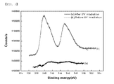
- FIG. 3 is a graph showing the results of the adsorption of a precious metal catalyst (for example, Pd°) using X-ray photoelectron spectroscopy (XPS) after UV irradiation according to the present invention.
- a precious metal catalyst for example, Pd°
- XPS X-ray photoelectron spectroscopy
- the present invention is directed to a method of selectively adsorbing a precious metal catalyst on the surface of a polymer. More concretely, the present invention is directed to a method of selectively adsorbing a precious metal catalyst on polymer surface, including the steps of: 1) masking the surface of a polymer adsorbed with photosensitive metal ions with a photomask and then irradiating the surface of the polymer with a light source to oxidize the photosensitive metal ions which are on the non-masked surface of the polymer; and 2) reacting the photosensitive metal ions not oxidized in step 1) with a precious metal catalyst to adsorb the precious metal catalyst on the surface of the polymer.
- the polymer used in the present invention includes polyimide, polyethylene terephthalate (PET) and aramid film, and is used to fabricate a flexible copper clad laminate (FCCL) which is an intermediate material used in a flexible printed circuit board (FPCB), to form an electronic circuit pattern or to prevent electromagnetic interference (EMI). It is preferred that the polymer used in the present invention be a polymer adsorbed with photosensitive metal ions.
- the photosensitive metal ions are metal ions causing a photochemical reaction using a light source, and, concretely, include titanium (Ti) ions, molybdenum (Mo) ions, tungsten (W) ions and tin (Sn) ions.
- Ti titanium
- Mo molybdenum
- W tungsten
- Sn tin
- a polymer whose surface is adsorbed with tin ions is used as the polymer.
- the method of adsorbing the photosensitive metal ions on the surface of the polymer may be conducted using the methods well known in the related field, preferably, the method disclosed in Korea Patent Application No. 2007-0003316 , filed by the present inventors.
- the method of adsorbing the photosensitive metal ions on the surface of the polymer may include the steps of: immersing the surface of the polymer into an alkali metal compound solution (for example, alkali metal hydroxide, alkali earth metal hydroxide or the like) or spraying the alkali metal compound solution onto the surface of the polymer to hydrophilize the surface of the polymer; providing functional groups onto the surface of the polymer to modify the surface of the polymer; and immersing the modified surface of the polymer into a solution containing photosensitive metal ions or spraying the solution onto the modified surface of the polymer.
- an alkali metal compound solution for example, alkali metal hydroxide, alkali earth metal hydroxide or the like
- the precious metal catalyst used in the present invention is silver (Ag), palladium (Pd), platinum (Pt), gold (Au) or the like.
- FIG. 1 shows a method of selectively adsorbing a precious metal on the surface of a polymer adsorbed with photosensitive metal ions according to an embodiment of the present invention.
- the method of selectively adsorbing a precious metal on the surface of a polymer will be described in detailed steps with reference to FIG. 1 .
- the surface of a polymer adsorbed with photosensitive metal ions is masked with a photomask, and then the surface of the polymer is irradiated with a light source to oxidize the photosensitive metal ions which are on the non-masked surface of the polymer.
- the specific portion of the surface of the polymer adsorbed with photosensitive metal ions that is, the portion of the surface of the polymer to be adsorbed with photosensitive metal ions, is masked with a photomask to block a light source, and the portion which is not blocked by the light source is irradiated with the light source to oxidize the photosensitive metal ions.
- the light source may be ultraviolet (UV) and have a wavelength of 200 ⁇ 450 nm, preferably, 300 ⁇ 420 nm. When the wavelength of the light source is below 200 nm, there is a problem in that manufacturing costs increase because the light source is expensive.
- the irradiation intensity of the light source is 10 - 30 mW/cm 2 .
- the photosensitive metal ions which are not oxidized in the first step are reacted with a precious metal catalyst to adsorb the precious metal catalyst on the surface of the polymer.
- a solution containing the precious metal catalyst is brought into contact with the surface of the polymer, and thus the photosensitive metal ions which are not oxidized by blocking the light source using the photomask in the first step are reacted with the precious metal catalyst to adsorb the precious metal catalyst on the surface of the polymer.
- this step is called an activation process.
- the activation process may be performed at a temperature of 20 - 50°C, preferably, 20 - 30°C for 20 seconds - 5 minutes, preferably, 30 seconds - 2 minutes such that the precious metal catalyst is sufficiently adsorbed on the surface of the polymer.
- a metal circuit pattern can be easily formed on the surface of the polymer by wet surface treatment such as electroless plating or the like.
- the wet surface treatment such as electroless plating or the like may be conducted using a method known in the related field.
- the polymer including the metal circuit pattern formed in this way can be easily used in automobiles, electronics, communications and semiconductors requiring micro-circuit boards because copper, nickel or the like adheres thinly and closely to the surface thereof.
- Example 1 The surface of the polymer of Example 1 was immersed in a precious metal catalyst solution having the composition given in Table 2. Palladium ions (Pd 2+ ) were reduced to palladium (Pd°) to be adsorbed on the surface of the polymer. The changes of the palladium ions depending on whether the photochemical reaction was conducted or not were analyzed using X-ray photoelectron spectroscopy (XPS), and the results thereof are shown in FIG. 3 . [Table 2] PdCl 2 HCl 0.03mol/l 0.02mol/l Temperature: 18 ⁇ 25°C, treatment time: 30 seconds
- the polymer adsorbed with a precious metal catalyst, prepared using the method of the present invention is advantageous in that various shapes of metal pattern layers can be simply and easily formed on the surface thereof, and a metal circuit layer made of copper, nickel or the like adheres closely to the surface thereof, and thus it can be easily used in automobiles, electronics, communications and semiconductors requiring micro-circuit boards.
Landscapes
- Chemical & Material Sciences (AREA)
- Chemical Kinetics & Catalysis (AREA)
- Engineering & Computer Science (AREA)
- Organic Chemistry (AREA)
- General Chemical & Material Sciences (AREA)
- Materials Engineering (AREA)
- Mechanical Engineering (AREA)
- Metallurgy (AREA)
- Physics & Mathematics (AREA)
- General Physics & Mathematics (AREA)
- Manufacturing & Machinery (AREA)
- Toxicology (AREA)
- Inorganic Chemistry (AREA)
- Health & Medical Sciences (AREA)
- Microelectronics & Electronic Packaging (AREA)
- Spectroscopy & Molecular Physics (AREA)
- Chemically Coating (AREA)
- Catalysts (AREA)
Abstract
The present invention relates to a method for the selective adsorption of a noble metal catalyst onto a surface of a polymer. More particularly, the method of the present invention includes a first step of masking with a photomask, the surface of a polymer adsorbed with a photosensitive metal ion, and radiating light onto the surface of the polymer such that the photosensitive metal ion on the unmasked surface is oxidized, and a second step of permitting the photosensitive metal ion which is not oxidized in the first step to react to a noble metal catalyst such that the noble metal catalyst is adsorbed onto the surface of the polymer.
Description
- The present invention relates to a method of selectively adsorbing a precious metal catalyst on polymer surface. A polymer film including a metal layer having a predetermined form can be manufactured using the method.
- Currently, as a technology for forming a metal circuit pattern on a polymer material such as polyimide (PI), polyethylene terephthalate (PET) or the like, which is used as a dielectric for flexible circuit boards or packages, a method of forming a metal circuit pattern by forming a predetermined circuit pattern on the surface of a polymer clad or deposited with thin copper foil using photoresist processing and then etching the copper foil is widely used.
- Such a conventional technology used to form a metal circuit pattern is problematic in that it is complicated, it includes long unit processes, it needs high-priced equipment, and it causes environmental pollution due to the formation of a corrosive etching solution. Further, this conventional technology used to form a metal circuit pattern is problematic in that cheap raw materials and expensive precise equipment are additionally required to realize a micro-circuit pattern or it is very difficult to realize the micro-circuit pattern.
- Meanwhile, methods of forming a metal layer on a polymer material are conducted by a laminating or casting process. In the laminating or casting process, a polymer material is surface-modified by plasma ions, and then a conductive metal junction layer is formed on the surface of the surface-modified polymer material using a dry surface treatment technology such as sputtering, metal deposition or the like, and then a metal coating layer is formed on the surface of the conductive metal junction layer using an electroplating technology or a copper film is directly bonded to the surface of the polymer material.
- Recently, a process of metalizing a polymer film using wet surface treatment has been developed. In this process, a metal circuit is also formed by forming a metal layer on a polymer material and then etching the metal layer with copper using photoresist processing. However, this process is also problematic in that it is not easy to form a relatively uniform metal layer, and in that high production expenses are incurred.
- Thus, the present inventors found that the above problems can be solved by using a method of adsorbing a precious metal catalyst on a polymer film during wet surface treatment. Based on this finding, the present invention was completed.
- An object of the present invention is to provide a method of selectively adsorbing a precious metal catalyst on polymer surface.
- Another object of the present invention is to provide a polymer film including a metal layer formed by wet-plating the polymer on which the precious metal catalyst is selectively adsorbed using the method.
- The polymer adsorbed with the precious metal catalyst, prepared using the method of the present invention, is advantageous in that various shapes of metal pattern layers can be simply and easily formed on the surface thereof, and a metal circuit layer made of copper, nickel or the like adheres closely to the surface thereof, and thus it can be easily used in automobiles, electronics, communications and semiconductors requiring micro-circuit boards. Further, when the polymer is prepared using the method of the present invention, there is an advantage in that the manufacturing cost thereof becomes low compared to conventional technologies, and expensive equipment is not required.
-
-
FIG. 1 is a process view showing a method of selectively adsorbing a precious metal on the surface of a polymer adsorbed with photosensitive metal ions according to an embodiment of the present invention; -
FIG. 2 is a graph showing the changes in the chemical structure of tin (Sn) ions by a photochemical reaction using X-ray photoelectron spectroscopy (XPS) after UV irradiation according to the present invention; and -
FIG. 3 is a graph showing the results of the adsorption of a precious metal catalyst (for example, Pd°) using X-ray photoelectron spectroscopy (XPS) after UV irradiation according to the present invention. - In an aspect, the present invention is directed to a method of selectively adsorbing a precious metal catalyst on the surface of a polymer. More concretely, the present invention is directed to a method of selectively adsorbing a precious metal catalyst on polymer surface, including the steps of: 1) masking the surface of a polymer adsorbed with photosensitive metal ions with a photomask and then irradiating the surface of the polymer with a light source to oxidize the photosensitive metal ions which are on the non-masked surface of the polymer; and 2) reacting the photosensitive metal ions not oxidized in step 1) with a precious metal catalyst to adsorb the precious metal catalyst on the surface of the polymer.
- The polymer used in the present invention includes polyimide, polyethylene terephthalate (PET) and aramid film, and is used to fabricate a flexible copper clad laminate (FCCL) which is an intermediate material used in a flexible printed circuit board (FPCB), to form an electronic circuit pattern or to prevent electromagnetic interference (EMI). It is preferred that the polymer used in the present invention be a polymer adsorbed with photosensitive metal ions.
- The photosensitive metal ions are metal ions causing a photochemical reaction using a light source, and, concretely, include titanium (Ti) ions, molybdenum (Mo) ions, tungsten (W) ions and tin (Sn) ions. In the embodiment of the present invention, a polymer whose surface is adsorbed with tin ions is used as the polymer. The method of adsorbing the photosensitive metal ions on the surface of the polymer may be conducted using the methods well known in the related field, preferably, the method disclosed in Korea Patent Application No.
2007-0003316 - The precious metal catalyst used in the present invention is silver (Ag), palladium (Pd), platinum (Pt), gold (Au) or the like.
-
FIG. 1 shows a method of selectively adsorbing a precious metal on the surface of a polymer adsorbed with photosensitive metal ions according to an embodiment of the present invention. Hereinafter, the method of selectively adsorbing a precious metal on the surface of a polymer will be described in detailed steps with reference toFIG. 1 . - Fist, the surface of a polymer adsorbed with photosensitive metal ions is masked with a photomask, and then the surface of the polymer is irradiated with a light source to oxidize the photosensitive metal ions which are on the non-masked surface of the polymer.
- Concretely, the specific portion of the surface of the polymer adsorbed with photosensitive metal ions, that is, the portion of the surface of the polymer to be adsorbed with photosensitive metal ions, is masked with a photomask to block a light source, and the portion which is not blocked by the light source is irradiated with the light source to oxidize the photosensitive metal ions. The light source may be ultraviolet (UV) and have a wavelength of 200 ∼ 450 nm, preferably, 300 ∼ 420 nm. When the wavelength of the light source is below 200 nm, there is a problem in that manufacturing costs increase because the light source is expensive. Further, when the wavelength thereof is above 450 nm, there is a problem in that the oxidation of the photosensitive metal compound, that is, a photochemical reaction, is very slowly conducted or does not proceed at all. Further, the irradiation intensity of the light source is 10 - 30 mW/cm2 .
- Second, the photosensitive metal ions which are not oxidized in the first step are reacted with a precious metal catalyst to adsorb the precious metal catalyst on the surface of the polymer.
- Concretely, a solution containing the precious metal catalyst is brought into contact with the surface of the polymer, and thus the photosensitive metal ions which are not oxidized by blocking the light source using the photomask in the first step are reacted with the precious metal catalyst to adsorb the precious metal catalyst on the surface of the polymer. For convenience, this step is called an activation process. The activation process may be performed at a temperature of 20 - 50°C, preferably, 20 - 30°C for 20 seconds - 5 minutes, preferably, 30 seconds - 2 minutes such that the precious metal catalyst is sufficiently adsorbed on the surface of the polymer.
- When the polymer adsorbed with a precious metal catalyst, prepared using the above method, is used, a metal circuit pattern can be easily formed on the surface of the polymer by wet surface treatment such as electroless plating or the like. The wet surface treatment such as electroless plating or the like may be conducted using a method known in the related field. The polymer including the metal circuit pattern formed in this way can be easily used in automobiles, electronics, communications and semiconductors requiring micro-circuit boards because copper, nickel or the like adheres thinly and closely to the surface thereof.
- Hereinafter, the present invention will be described in more detail with reference to the following Examples. However, the scope of the present invention is not limited thereto.
- Polyimide (PI) or polyethylene terephthalate (PET), as a polymer, was immersed in a photosensitive metal ion-containing solution having the composition given in Table 1 below for 4 - 8 minutes, and then tin ions (Sn2+), which are photosensitive metal ions, were adsorbed on the surface of the polymer. Subsequently, a photomask was disposed on the surface of the polymer adsorbed with the tin ions (Sn2+), and the surface thereof was irradiated with ultraviolet (UV) light having a wavelength of 365 nm. The tin ions (Sn2+) which are on the UV-irradiated surface of the polymer were oxidized into tin ions (Sn4+) by a photochemical reaction. The changes of the tin ions depending on whether the photochemical reaction was conducted or not were analyzed using X-ray photoelectron spectroscopy (XPS), and the results thereof are shown in
FIG. 2 .[Table 1] SnCl2 HCl 0.3∼0.6mol/l 0.08mol/l Temperature: 18∼25°C, treatment time: 4∼8 minutes - The surface of the polymer of Example 1 was immersed in a precious metal catalyst solution having the composition given in Table 2. Palladium ions (Pd2+) were reduced to palladium (Pd°) to be adsorbed on the surface of the polymer. The changes of the palladium ions depending on whether the photochemical reaction was conducted or not were analyzed using X-ray photoelectron spectroscopy (XPS), and the results thereof are shown in
FIG. 3 .[Table 2] PdCl2 HCl 0.03mol/l 0.02mol/l Temperature: 18∼25°C, treatment time: 30 seconds - The polymer adsorbed with a precious metal catalyst, prepared using the method of the present invention, is advantageous in that various shapes of metal pattern layers can be simply and easily formed on the surface thereof, and a metal circuit layer made of copper, nickel or the like adheres closely to the surface thereof, and thus it can be easily used in automobiles, electronics, communications and semiconductors requiring micro-circuit boards.
Claims (7)
- A method of selectively adsorbing a precious metal catalyst on a polymer surface, comprising the steps of:1) masking a surface of a polymer adsorbed with a photosensitive metal ions with a photomask and then irradiating the surface of the polymer with a light source to oxidize photosensitive metal ions which are on the non-masked surface of the polymer; and2) reacting the photosensitive metal ion not oxidized in step 1) with a precious metal catalyst to adsorb the precious metal catalyst on the surface of the polymer.
- The method according to claim 1, wherein the polymer is any one selected from the group consisting of polyimide (PI), polyethylene terephthalate (PET), and aramid film.
- The method according to claim 1, wherein the photosensitive ion is any one selected from the group consisting of titanium (Ti) ion, molybdenum (Mo) ion, tungsten (W) ion, and tin (Sn) ion.
- The method according to claim 1, wherein the light source is an ultraviolet (UV) light source.
- The method according to claim 4, wherein the ultraviolet (UV) light source has a wavelength of 200 ∼ 450 nm.
- The method according to claim 1, wherein the precious metal catalyst is any one selected from the group consisting of silver (Ag), palladium (Pd), platinum (Pt), and gold (Au).
- The method according to claim 1, wherein the step 2) is performed at a temperature of 20 - 50°C for 20 seconds - 5 minutes.
Applications Claiming Priority (2)
| Application Number | Priority Date | Filing Date | Title |
|---|---|---|---|
| KR1020080008626A KR100904251B1 (en) | 2008-01-28 | 2008-01-28 | Selective Adsorption of Precious Metal Catalysts on Polymer Surface |
| PCT/KR2009/000384 WO2009096691A2 (en) | 2008-01-28 | 2009-01-23 | Method for selective adsorption of noble metal catalyst onto surface of polymer |
Publications (2)
| Publication Number | Publication Date |
|---|---|
| EP2239630A2 true EP2239630A2 (en) | 2010-10-13 |
| EP2239630A4 EP2239630A4 (en) | 2011-03-16 |
Family
ID=40913401
Family Applications (1)
| Application Number | Title | Priority Date | Filing Date |
|---|---|---|---|
| EP09706192A Withdrawn EP2239630A4 (en) | 2008-01-28 | 2009-01-23 | METHOD FOR THE SELECTIVE ADSORPTION OF A NOBLE METAL CATALYST ON THE SURFACE OF A POLYMER |
Country Status (4)
| Country | Link |
|---|---|
| US (1) | US20100307796A1 (en) |
| EP (1) | EP2239630A4 (en) |
| KR (1) | KR100904251B1 (en) |
| WO (1) | WO2009096691A2 (en) |
Family Cites Families (19)
| Publication number | Priority date | Publication date | Assignee | Title |
|---|---|---|---|---|
| US3573973A (en) * | 1967-11-13 | 1971-04-06 | Ibm | High speed additive circuit process |
| US3562005A (en) * | 1968-04-09 | 1971-02-09 | Western Electric Co | Method of generating precious metal-reducing patterns |
| USRE29015E (en) * | 1968-04-09 | 1976-10-26 | Western Electric Company, Inc. | Method of generating precious metal-reducing patterns |
| CA956850A (en) * | 1970-03-16 | 1974-10-29 | Frederick W. Schneble (Jr.) | Direct bonding of electroless metals to substrates |
| US3776770A (en) * | 1971-10-08 | 1973-12-04 | Western Electric Co | Method of selectively depositing a metal on a surface of a substrate |
| US3783005A (en) * | 1972-02-04 | 1974-01-01 | Western Electric Co | Method of depositing a metal on a surface of a nonconductive substrate |
| US3950570A (en) * | 1974-05-02 | 1976-04-13 | Western Electric Company, Inc. | Method of depositing a metal on a surface |
| US3928670A (en) * | 1974-09-23 | 1975-12-23 | Amp Inc | Selective plating on non-metallic surfaces |
| US3934335A (en) * | 1974-10-16 | 1976-01-27 | Texas Instruments Incorporated | Multilayer printed circuit board |
| JPH02219858A (en) * | 1989-02-22 | 1990-09-03 | Idemitsu Petrochem Co Ltd | Polyarylene sulfide resin composition and molding produced therefrom |
| BE1007610A3 (en) * | 1993-10-11 | 1995-08-22 | Philips Electronics Nv | METHOD FOR ENERGIZE APPLYING A PATTERN ON METAL an electrically insulating substrate. |
| DE69841945D1 (en) * | 1997-08-08 | 2010-11-25 | Dainippon Printing Co Ltd | Structure for patterning, patterning and their application |
| JP4413035B2 (en) | 1997-08-08 | 2010-02-10 | 大日本印刷株式会社 | Pattern forming body and pattern forming method |
| JP2000144437A (en) | 1998-11-17 | 2000-05-26 | Hitachi Ltd | Electroless plating method, electroless plating apparatus, wiring board manufacturing method, and wiring board manufacturing apparatus |
| JP2002241950A (en) | 2001-02-14 | 2002-08-28 | Learonal Japan Inc | Direct patterning method |
| US20040101665A1 (en) * | 2001-02-14 | 2004-05-27 | Shipley Company, L.L.C. | Direct patterning method |
| KR100959751B1 (en) * | 2003-05-13 | 2010-05-25 | 삼성전자주식회사 | Metal pattern formation method and electromagnetic shielding filter using the same |
| KR100741041B1 (en) | 2005-07-01 | 2007-07-20 | 박중옥 | Green tea dumplings and manufacturing method |
| KR100815376B1 (en) * | 2006-08-17 | 2008-03-19 | 삼성전자주식회사 | Novel metal pattern manufacturing method and flat panel display device using same |
-
2008
- 2008-01-28 KR KR1020080008626A patent/KR100904251B1/en not_active Expired - Fee Related
-
2009
- 2009-01-23 EP EP09706192A patent/EP2239630A4/en not_active Withdrawn
- 2009-01-23 WO PCT/KR2009/000384 patent/WO2009096691A2/en not_active Ceased
-
2010
- 2010-07-28 US US12/845,656 patent/US20100307796A1/en not_active Abandoned
Also Published As
| Publication number | Publication date |
|---|---|
| US20100307796A1 (en) | 2010-12-09 |
| KR100904251B1 (en) | 2009-06-25 |
| WO2009096691A2 (en) | 2009-08-06 |
| EP2239630A4 (en) | 2011-03-16 |
| WO2009096691A3 (en) | 2009-10-29 |
Similar Documents
| Publication | Publication Date | Title |
|---|---|---|
| KR100759069B1 (en) | Resin substrate having a resin-metal composite layer and method for manufacturing thereof | |
| EP2453040B1 (en) | Method for producing formed circuit component | |
| US20110292622A1 (en) | Method for electric circuit deposition | |
| US20060068173A1 (en) | Methods for forming and patterning of metallic films | |
| JP3486864B2 (en) | Method for forming copper wiring on substrate and substrate on which copper wiring is formed | |
| EP0259754A2 (en) | Flexible circuits | |
| JP3999696B2 (en) | Electroless plating method and plated parts | |
| US20180332713A1 (en) | Patterning of electroless metals by selective deactivation of catalysts | |
| JP2007180089A (en) | Method for manufacturing resin molded part having circuit conductor pattern | |
| JP2006210891A (en) | Forming method of inorganic thin film pattern for polyimide resin | |
| EP2239630A2 (en) | Method for selective adsorption of noble metal catalyst onto surface of polymer | |
| JP2005045236A (en) | Inorganic thin film pattern forming method of polyimide resin | |
| KR20060064549A (en) | Inorganic thin film formation method of polyimide resin and manufacturing method of polyimide resin for surface modified inorganic thin film formation | |
| JP4332795B2 (en) | Electroless plating method | |
| KR100877379B1 (en) | Selective Metallization Process on Non-Conductive Dielectrics | |
| JP2019123910A (en) | Formation method of front and rear surfaces of fine circuit pattern | |
| KR101907074B1 (en) | Method for forming metallic pattern on non-conductive dielectric substrates in micro scale | |
| KR101583007B1 (en) | A method for forming metal pattern on synthetic resin | |
| JP2005281766A (en) | Electroless plating method and its utilization | |
| JP4955274B2 (en) | Plating wiring board and electroless plating method | |
| JP2007207867A (en) | Substrate having metal film, its production process, electronic component employing the substrate and its manufacturing process | |
| JP2006219715A (en) | Metal plating method for heat-resistant insulating resin | |
| JPH0810786B2 (en) | Method of forming conductor pattern by ultraviolet laser | |
| KR20100068787A (en) | Printed circuit board and method for fabricating the same | |
| JP2007100134A (en) | Inorganic thin film pattern forming method |
Legal Events
| Date | Code | Title | Description |
|---|---|---|---|
| PUAI | Public reference made under article 153(3) epc to a published international application that has entered the european phase |
Free format text: ORIGINAL CODE: 0009012 |
|
| 17P | Request for examination filed |
Effective date: 20100722 |
|
| AK | Designated contracting states |
Kind code of ref document: A2 Designated state(s): AT BE BG CH CY CZ DE DK EE ES FI FR GB GR HR HU IE IS IT LI LT LU LV MC MK MT NL NO PL PT RO SE SI SK TR |
|
| AX | Request for extension of the european patent |
Extension state: AL BA RS |
|
| A4 | Supplementary search report drawn up and despatched |
Effective date: 20110214 |
|
| DAX | Request for extension of the european patent (deleted) | ||
| STAA | Information on the status of an ep patent application or granted ep patent |
Free format text: STATUS: THE APPLICATION HAS BEEN WITHDRAWN |
|
| 18W | Application withdrawn |
Effective date: 20110830 |