EP2239604A1 - Opto-electric hybrid board and electronic device - Google Patents
Opto-electric hybrid board and electronic device Download PDFInfo
- Publication number
- EP2239604A1 EP2239604A1 EP08871802A EP08871802A EP2239604A1 EP 2239604 A1 EP2239604 A1 EP 2239604A1 EP 08871802 A EP08871802 A EP 08871802A EP 08871802 A EP08871802 A EP 08871802A EP 2239604 A1 EP2239604 A1 EP 2239604A1
- Authority
- EP
- European Patent Office
- Prior art keywords
- opto
- electric hybrid
- optical waveguide
- flexible
- hybrid board
- Prior art date
- Legal status (The legal status is an assumption and is not a legal conclusion. Google has not performed a legal analysis and makes no representation as to the accuracy of the status listed.)
- Withdrawn
Links
- 230000003287 optical effect Effects 0.000 claims abstract description 93
- 230000003014 reinforcing effect Effects 0.000 claims abstract description 48
- 238000005452 bending Methods 0.000 claims description 53
- 239000011347 resin Substances 0.000 claims description 43
- 229920005989 resin Polymers 0.000 claims description 43
- 239000000758 substrate Substances 0.000 claims description 25
- 229920001721 polyimide Polymers 0.000 claims description 15
- 239000004760 aramid Substances 0.000 claims description 6
- 229920003235 aromatic polyamide Polymers 0.000 claims description 6
- 239000009719 polyimide resin Substances 0.000 claims description 5
- OKTJSMMVPCPJKN-UHFFFAOYSA-N Carbon Chemical compound [C] OKTJSMMVPCPJKN-UHFFFAOYSA-N 0.000 claims description 4
- 229910052799 carbon Inorganic materials 0.000 claims description 4
- 239000011521 glass Substances 0.000 claims description 3
- 239000010410 layer Substances 0.000 description 29
- 230000001070 adhesive effect Effects 0.000 description 21
- 239000000853 adhesive Substances 0.000 description 20
- 238000000034 method Methods 0.000 description 20
- 230000005540 biological transmission Effects 0.000 description 16
- -1 vinylidene halide Chemical class 0.000 description 16
- 238000004519 manufacturing process Methods 0.000 description 11
- 239000004642 Polyimide Substances 0.000 description 10
- 150000001875 compounds Chemical class 0.000 description 10
- 239000012792 core layer Substances 0.000 description 10
- 239000003960 organic solvent Substances 0.000 description 10
- 230000008901 benefit Effects 0.000 description 9
- 238000011161 development Methods 0.000 description 9
- 230000018109 developmental process Effects 0.000 description 9
- 238000011156 evaluation Methods 0.000 description 9
- 239000007788 liquid Substances 0.000 description 9
- 239000000463 material Substances 0.000 description 9
- 230000001681 protective effect Effects 0.000 description 9
- 239000012790 adhesive layer Substances 0.000 description 8
- 230000008093 supporting effect Effects 0.000 description 8
- 238000012360 testing method Methods 0.000 description 8
- 239000007864 aqueous solution Substances 0.000 description 7
- 238000010438 heat treatment Methods 0.000 description 7
- 239000003999 initiator Substances 0.000 description 7
- ZMXDDKWLCZADIW-UHFFFAOYSA-N N,N-Dimethylformamide Chemical compound CN(C)C=O ZMXDDKWLCZADIW-UHFFFAOYSA-N 0.000 description 6
- 229920005601 base polymer Polymers 0.000 description 6
- 239000000835 fiber Substances 0.000 description 6
- 239000012779 reinforcing material Substances 0.000 description 6
- NIXOWILDQLNWCW-UHFFFAOYSA-M Acrylate Chemical compound [O-]C(=O)C=C NIXOWILDQLNWCW-UHFFFAOYSA-M 0.000 description 5
- 229920002799 BoPET Polymers 0.000 description 5
- KFZMGEQAYNKOFK-UHFFFAOYSA-N Isopropanol Chemical compound CC(C)O KFZMGEQAYNKOFK-UHFFFAOYSA-N 0.000 description 5
- 230000000052 comparative effect Effects 0.000 description 5
- 230000008878 coupling Effects 0.000 description 5
- 238000010168 coupling process Methods 0.000 description 5
- 238000005859 coupling reaction Methods 0.000 description 5
- 230000007246 mechanism Effects 0.000 description 5
- 229920003223 poly(pyromellitimide-1,4-diphenyl ether) Polymers 0.000 description 5
- 238000003825 pressing Methods 0.000 description 5
- 239000011342 resin composition Substances 0.000 description 5
- 239000000243 solution Substances 0.000 description 5
- 239000002904 solvent Substances 0.000 description 5
- 239000000126 substance Substances 0.000 description 5
- CSCPPACGZOOCGX-UHFFFAOYSA-N Acetone Chemical compound CC(C)=O CSCPPACGZOOCGX-UHFFFAOYSA-N 0.000 description 4
- IISBACLAFKSPIT-UHFFFAOYSA-N bisphenol A Chemical compound C=1C=C(O)C=CC=1C(C)(C)C1=CC=C(O)C=C1 IISBACLAFKSPIT-UHFFFAOYSA-N 0.000 description 4
- 239000011248 coating agent Substances 0.000 description 4
- 238000000576 coating method Methods 0.000 description 4
- 238000001723 curing Methods 0.000 description 4
- JHIVVAPYMSGYDF-UHFFFAOYSA-N cyclohexanone Chemical compound O=C1CCCCC1 JHIVVAPYMSGYDF-UHFFFAOYSA-N 0.000 description 4
- 238000010030 laminating Methods 0.000 description 4
- 239000013307 optical fiber Substances 0.000 description 4
- 230000002093 peripheral effect Effects 0.000 description 4
- 229920000139 polyethylene terephthalate Polymers 0.000 description 4
- 239000005020 polyethylene terephthalate Substances 0.000 description 4
- 229920000642 polymer Polymers 0.000 description 4
- 238000002834 transmittance Methods 0.000 description 4
- ZWEHNKRNPOVVGH-UHFFFAOYSA-N 2-Butanone Chemical compound CCC(C)=O ZWEHNKRNPOVVGH-UHFFFAOYSA-N 0.000 description 3
- GJKGAPPUXSSCFI-UHFFFAOYSA-N 2-Hydroxy-4'-(2-hydroxyethoxy)-2-methylpropiophenone Chemical compound CC(C)(O)C(=O)C1=CC=C(OCCO)C=C1 GJKGAPPUXSSCFI-UHFFFAOYSA-N 0.000 description 3
- XEKOWRVHYACXOJ-UHFFFAOYSA-N Ethyl acetate Chemical compound CCOC(C)=O XEKOWRVHYACXOJ-UHFFFAOYSA-N 0.000 description 3
- FXHOOIRPVKKKFG-UHFFFAOYSA-N N,N-Dimethylacetamide Chemical compound CN(C)C(C)=O FXHOOIRPVKKKFG-UHFFFAOYSA-N 0.000 description 3
- 239000004952 Polyamide Substances 0.000 description 3
- FAPWRFPIFSIZLT-UHFFFAOYSA-M Sodium chloride Chemical compound [Na+].[Cl-] FAPWRFPIFSIZLT-UHFFFAOYSA-M 0.000 description 3
- HEMHJVSKTPXQMS-UHFFFAOYSA-M Sodium hydroxide Chemical compound [OH-].[Na+] HEMHJVSKTPXQMS-UHFFFAOYSA-M 0.000 description 3
- YXFVVABEGXRONW-UHFFFAOYSA-N Toluene Chemical compound CC1=CC=CC=C1 YXFVVABEGXRONW-UHFFFAOYSA-N 0.000 description 3
- 239000003513 alkali Substances 0.000 description 3
- ISAOCJYIOMOJEB-UHFFFAOYSA-N desyl alcohol Natural products C=1C=CC=CC=1C(O)C(=O)C1=CC=CC=C1 ISAOCJYIOMOJEB-UHFFFAOYSA-N 0.000 description 3
- 239000003822 epoxy resin Substances 0.000 description 3
- 238000003475 lamination Methods 0.000 description 3
- QSHDDOUJBYECFT-UHFFFAOYSA-N mercury Chemical compound [Hg] QSHDDOUJBYECFT-UHFFFAOYSA-N 0.000 description 3
- 239000000203 mixture Substances 0.000 description 3
- 239000013034 phenoxy resin Substances 0.000 description 3
- 229920006287 phenoxy resin Polymers 0.000 description 3
- 229920002647 polyamide Polymers 0.000 description 3
- 229920000647 polyepoxide Polymers 0.000 description 3
- 230000002035 prolonged effect Effects 0.000 description 3
- LLHKCFNBLRBOGN-UHFFFAOYSA-N propylene glycol methyl ether acetate Chemical compound COCC(C)OC(C)=O LLHKCFNBLRBOGN-UHFFFAOYSA-N 0.000 description 3
- 230000009467 reduction Effects 0.000 description 3
- AZQWKYJCGOJGHM-UHFFFAOYSA-N 1,4-benzoquinone Chemical compound O=C1C=CC(=O)C=C1 AZQWKYJCGOJGHM-UHFFFAOYSA-N 0.000 description 2
- FRASJONUBLZVQX-UHFFFAOYSA-N 1,4-naphthoquinone Chemical compound C1=CC=C2C(=O)C=CC(=O)C2=C1 FRASJONUBLZVQX-UHFFFAOYSA-N 0.000 description 2
- HZAXFHJVJLSVMW-UHFFFAOYSA-N 2-Aminoethan-1-ol Chemical compound NCCO HZAXFHJVJLSVMW-UHFFFAOYSA-N 0.000 description 2
- UHFFVFAKEGKNAQ-UHFFFAOYSA-N 2-benzyl-2-(dimethylamino)-1-(4-morpholin-4-ylphenyl)butan-1-one Chemical compound C=1C=C(N2CCOCC2)C=CC=1C(=O)C(CC)(N(C)C)CC1=CC=CC=C1 UHFFVFAKEGKNAQ-UHFFFAOYSA-N 0.000 description 2
- JESXATFQYMPTNL-UHFFFAOYSA-N 2-ethenylphenol Chemical compound OC1=CC=CC=C1C=C JESXATFQYMPTNL-UHFFFAOYSA-N 0.000 description 2
- NJWGQARXZDRHCD-UHFFFAOYSA-N 2-methylanthraquinone Chemical compound C1=CC=C2C(=O)C3=CC(C)=CC=C3C(=O)C2=C1 NJWGQARXZDRHCD-UHFFFAOYSA-N 0.000 description 2
- UUEWCQRISZBELL-UHFFFAOYSA-N 3-trimethoxysilylpropane-1-thiol Chemical compound CO[Si](OC)(OC)CCCS UUEWCQRISZBELL-UHFFFAOYSA-N 0.000 description 2
- VVBLNCFGVYUYGU-UHFFFAOYSA-N 4,4'-Bis(dimethylamino)benzophenone Chemical compound C1=CC(N(C)C)=CC=C1C(=O)C1=CC=C(N(C)C)C=C1 VVBLNCFGVYUYGU-UHFFFAOYSA-N 0.000 description 2
- YEJRWHAVMIAJKC-UHFFFAOYSA-N 4-Butyrolactone Chemical compound O=C1CCCO1 YEJRWHAVMIAJKC-UHFFFAOYSA-N 0.000 description 2
- YYVYAPXYZVYDHN-UHFFFAOYSA-N 9,10-phenanthroquinone Chemical compound C1=CC=C2C(=O)C(=O)C3=CC=CC=C3C2=C1 YYVYAPXYZVYDHN-UHFFFAOYSA-N 0.000 description 2
- RYGMFSIKBFXOCR-UHFFFAOYSA-N Copper Chemical compound [Cu] RYGMFSIKBFXOCR-UHFFFAOYSA-N 0.000 description 2
- 239000004593 Epoxy Substances 0.000 description 2
- LFQSCWFLJHTTHZ-UHFFFAOYSA-N Ethanol Chemical compound CCO LFQSCWFLJHTTHZ-UHFFFAOYSA-N 0.000 description 2
- DGAQECJNVWCQMB-PUAWFVPOSA-M Ilexoside XXIX Chemical compound C[C@@H]1CC[C@@]2(CC[C@@]3(C(=CC[C@H]4[C@]3(CC[C@@H]5[C@@]4(CC[C@@H](C5(C)C)OS(=O)(=O)[O-])C)C)[C@@H]2[C@]1(C)O)C)C(=O)O[C@H]6[C@@H]([C@H]([C@@H]([C@H](O6)CO)O)O)O.[Na+] DGAQECJNVWCQMB-PUAWFVPOSA-M 0.000 description 2
- WHXSMMKQMYFTQS-UHFFFAOYSA-N Lithium Chemical compound [Li] WHXSMMKQMYFTQS-UHFFFAOYSA-N 0.000 description 2
- MJVAVZPDRWSRRC-UHFFFAOYSA-N Menadione Chemical compound C1=CC=C2C(=O)C(C)=CC(=O)C2=C1 MJVAVZPDRWSRRC-UHFFFAOYSA-N 0.000 description 2
- LRHPLDYGYMQRHN-UHFFFAOYSA-N N-Butanol Chemical compound CCCCO LRHPLDYGYMQRHN-UHFFFAOYSA-N 0.000 description 2
- IMNFDUFMRHMDMM-UHFFFAOYSA-N N-Heptane Chemical compound CCCCCCC IMNFDUFMRHMDMM-UHFFFAOYSA-N 0.000 description 2
- NPKSPKHJBVJUKB-UHFFFAOYSA-N N-phenylglycine Chemical compound OC(=O)CNC1=CC=CC=C1 NPKSPKHJBVJUKB-UHFFFAOYSA-N 0.000 description 2
- 239000004697 Polyetherimide Substances 0.000 description 2
- ZLMJMSJWJFRBEC-UHFFFAOYSA-N Potassium Chemical compound [K] ZLMJMSJWJFRBEC-UHFFFAOYSA-N 0.000 description 2
- CDBYLPFSWZWCQE-UHFFFAOYSA-L Sodium Carbonate Chemical compound [Na+].[Na+].[O-]C([O-])=O CDBYLPFSWZWCQE-UHFFFAOYSA-L 0.000 description 2
- 235000000126 Styrax benzoin Nutrition 0.000 description 2
- 244000028419 Styrax benzoin Species 0.000 description 2
- 235000008411 Sumatra benzointree Nutrition 0.000 description 2
- GUCYFKSBFREPBC-UHFFFAOYSA-N [phenyl-(2,4,6-trimethylbenzoyl)phosphoryl]-(2,4,6-trimethylphenyl)methanone Chemical compound CC1=CC(C)=CC(C)=C1C(=O)P(=O)(C=1C=CC=CC=1)C(=O)C1=C(C)C=C(C)C=C1C GUCYFKSBFREPBC-UHFFFAOYSA-N 0.000 description 2
- 239000002518 antifoaming agent Substances 0.000 description 2
- 239000002585 base Substances 0.000 description 2
- 229960002130 benzoin Drugs 0.000 description 2
- 239000011230 binding agent Substances 0.000 description 2
- PXKLMJQFEQBVLD-UHFFFAOYSA-N bisphenol F Chemical compound C1=CC(O)=CC=C1CC1=CC=C(O)C=C1 PXKLMJQFEQBVLD-UHFFFAOYSA-N 0.000 description 2
- 229910021538 borax Inorganic materials 0.000 description 2
- 230000001680 brushing effect Effects 0.000 description 2
- 238000004891 communication Methods 0.000 description 2
- 229910052802 copper Inorganic materials 0.000 description 2
- 239000010949 copper Substances 0.000 description 2
- 238000005336 cracking Methods 0.000 description 2
- 230000007423 decrease Effects 0.000 description 2
- 238000001035 drying Methods 0.000 description 2
- 229920001971 elastomer Polymers 0.000 description 2
- 238000005516 engineering process Methods 0.000 description 2
- 230000002349 favourable effect Effects 0.000 description 2
- 235000019382 gum benzoic Nutrition 0.000 description 2
- 229910052744 lithium Inorganic materials 0.000 description 2
- 229920001684 low density polyethylene Polymers 0.000 description 2
- 239000004702 low-density polyethylene Substances 0.000 description 2
- 229910052753 mercury Inorganic materials 0.000 description 2
- 229920003986 novolac Polymers 0.000 description 2
- QWVGKYWNOKOFNN-UHFFFAOYSA-N o-cresol Chemical compound CC1=CC=CC=C1O QWVGKYWNOKOFNN-UHFFFAOYSA-N 0.000 description 2
- 238000000016 photochemical curing Methods 0.000 description 2
- 229920001601 polyetherimide Polymers 0.000 description 2
- 229910052700 potassium Inorganic materials 0.000 description 2
- 239000011591 potassium Substances 0.000 description 2
- BWHMMNNQKKPAPP-UHFFFAOYSA-L potassium carbonate Chemical compound [K+].[K+].[O-]C([O-])=O BWHMMNNQKKPAPP-UHFFFAOYSA-L 0.000 description 2
- 238000007790 scraping Methods 0.000 description 2
- 230000008054 signal transmission Effects 0.000 description 2
- 229910052708 sodium Inorganic materials 0.000 description 2
- 239000011734 sodium Substances 0.000 description 2
- 239000004328 sodium tetraborate Substances 0.000 description 2
- 235000010339 sodium tetraborate Nutrition 0.000 description 2
- 239000007921 spray Substances 0.000 description 2
- 239000004094 surface-active agent Substances 0.000 description 2
- WGTYBPLFGIVFAS-UHFFFAOYSA-M tetramethylammonium hydroxide Chemical compound [OH-].C[N+](C)(C)C WGTYBPLFGIVFAS-UHFFFAOYSA-M 0.000 description 2
- LWIHDJKSTIGBAC-UHFFFAOYSA-K tripotassium phosphate Chemical compound [K+].[K+].[K+].[O-]P([O-])([O-])=O LWIHDJKSTIGBAC-UHFFFAOYSA-K 0.000 description 2
- XLYOFNOQVPJJNP-UHFFFAOYSA-N water Substances O XLYOFNOQVPJJNP-UHFFFAOYSA-N 0.000 description 2
- UOCLXMDMGBRAIB-UHFFFAOYSA-N 1,1,1-trichloroethane Chemical compound CC(Cl)(Cl)Cl UOCLXMDMGBRAIB-UHFFFAOYSA-N 0.000 description 1
- XHXSXTIIDBZEKB-UHFFFAOYSA-N 1,2,3,4,5,6,7,8-octamethylanthracene-9,10-dione Chemical compound CC1=C(C)C(C)=C2C(=O)C3=C(C)C(C)=C(C)C(C)=C3C(=O)C2=C1C XHXSXTIIDBZEKB-UHFFFAOYSA-N 0.000 description 1
- YPFDHNVEDLHUCE-UHFFFAOYSA-N 1,3-propanediol Substances OCCCO YPFDHNVEDLHUCE-UHFFFAOYSA-N 0.000 description 1
- LMGYOBQJBQAZKC-UHFFFAOYSA-N 1-(2-ethylphenyl)-2-hydroxy-2-phenylethanone Chemical compound CCC1=CC=CC=C1C(=O)C(O)C1=CC=CC=C1 LMGYOBQJBQAZKC-UHFFFAOYSA-N 0.000 description 1
- BOCJQSFSGAZAPQ-UHFFFAOYSA-N 1-chloroanthracene-9,10-dione Chemical compound O=C1C2=CC=CC=C2C(=O)C2=C1C=CC=C2Cl BOCJQSFSGAZAPQ-UHFFFAOYSA-N 0.000 description 1
- 239000012956 1-hydroxycyclohexylphenyl-ketone Substances 0.000 description 1
- ARXJGSRGQADJSQ-UHFFFAOYSA-N 1-methoxypropan-2-ol Chemical compound COCC(C)O ARXJGSRGQADJSQ-UHFFFAOYSA-N 0.000 description 1
- KWVGIHKZDCUPEU-UHFFFAOYSA-N 2,2-dimethoxy-2-phenylacetophenone Chemical compound C=1C=CC=CC=1C(OC)(OC)C(=O)C1=CC=CC=C1 KWVGIHKZDCUPEU-UHFFFAOYSA-N 0.000 description 1
- KIJPZYXCIHZVGP-UHFFFAOYSA-N 2,3-dimethylanthracene-9,10-dione Chemical compound O=C1C2=CC=CC=C2C(=O)C2=C1C=C(C)C(C)=C2 KIJPZYXCIHZVGP-UHFFFAOYSA-N 0.000 description 1
- LZWVPGJPVCYAOC-UHFFFAOYSA-N 2,3-diphenylanthracene-9,10-dione Chemical compound C=1C=CC=CC=1C=1C=C2C(=O)C3=CC=CC=C3C(=O)C2=CC=1C1=CC=CC=C1 LZWVPGJPVCYAOC-UHFFFAOYSA-N 0.000 description 1
- GSKOWRJEBKQTKZ-UHFFFAOYSA-N 2,6-dihydroxy-2,6-dimethylheptan-4-one Chemical compound CC(C)(O)CC(=O)CC(C)(C)O GSKOWRJEBKQTKZ-UHFFFAOYSA-N 0.000 description 1
- UCSGWEMRGIONEW-UHFFFAOYSA-N 2-(2-chlorophenyl)-4,5-bis(2-methoxyphenyl)-1h-imidazole Chemical class COC1=CC=CC=C1C1=C(C=2C(=CC=CC=2)OC)NC(C=2C(=CC=CC=2)Cl)=N1 UCSGWEMRGIONEW-UHFFFAOYSA-N 0.000 description 1
- NSWNXQGJAPQOID-UHFFFAOYSA-N 2-(2-chlorophenyl)-4,5-diphenyl-1h-imidazole Chemical class ClC1=CC=CC=C1C1=NC(C=2C=CC=CC=2)=C(C=2C=CC=CC=2)N1 NSWNXQGJAPQOID-UHFFFAOYSA-N 0.000 description 1
- SBASXUCJHJRPEV-UHFFFAOYSA-N 2-(2-methoxyethoxy)ethanol Chemical compound COCCOCCO SBASXUCJHJRPEV-UHFFFAOYSA-N 0.000 description 1
- XIOGJAPOAUEYJO-UHFFFAOYSA-N 2-(2-methoxyphenyl)-4,5-diphenyl-1h-imidazole Chemical class COC1=CC=CC=C1C1=NC(C=2C=CC=CC=2)=C(C=2C=CC=CC=2)N1 XIOGJAPOAUEYJO-UHFFFAOYSA-N 0.000 description 1
- SNFCQJAJPFWBDJ-UHFFFAOYSA-N 2-(4-methoxyphenyl)-4,5-diphenyl-1h-imidazole Chemical class C1=CC(OC)=CC=C1C1=NC(C=2C=CC=CC=2)=C(C=2C=CC=CC=2)N1 SNFCQJAJPFWBDJ-UHFFFAOYSA-N 0.000 description 1
- XNWFRZJHXBZDAG-UHFFFAOYSA-N 2-METHOXYETHANOL Chemical compound COCCO XNWFRZJHXBZDAG-UHFFFAOYSA-N 0.000 description 1
- YCPMSWJCWKUXRH-UHFFFAOYSA-N 2-[4-[9-[4-(2-prop-2-enoyloxyethoxy)phenyl]fluoren-9-yl]phenoxy]ethyl prop-2-enoate Chemical compound C1=CC(OCCOC(=O)C=C)=CC=C1C1(C=2C=CC(OCCOC(=O)C=C)=CC=2)C2=CC=CC=C2C2=CC=CC=C21 YCPMSWJCWKUXRH-UHFFFAOYSA-N 0.000 description 1
- KMNCBSZOIQAUFX-UHFFFAOYSA-N 2-ethoxy-1,2-diphenylethanone Chemical compound C=1C=CC=CC=1C(OCC)C(=O)C1=CC=CC=C1 KMNCBSZOIQAUFX-UHFFFAOYSA-N 0.000 description 1
- ZNQVEEAIQZEUHB-UHFFFAOYSA-N 2-ethoxyethanol Chemical compound CCOCCO ZNQVEEAIQZEUHB-UHFFFAOYSA-N 0.000 description 1
- SJEBAWHUJDUKQK-UHFFFAOYSA-N 2-ethylanthraquinone Chemical compound C1=CC=C2C(=O)C3=CC(CC)=CC=C3C(=O)C2=C1 SJEBAWHUJDUKQK-UHFFFAOYSA-N 0.000 description 1
- ZLBFNQGHAGAXDX-UHFFFAOYSA-N 2-hydroxy-1,2-diphenylethanone;phenol Chemical compound OC1=CC=CC=C1.C=1C=CC=CC=1C(O)C(=O)C1=CC=CC=C1 ZLBFNQGHAGAXDX-UHFFFAOYSA-N 0.000 description 1
- VZMLJEYQUZKERO-UHFFFAOYSA-N 2-hydroxy-1-(2-methylphenyl)-2-phenylethanone Chemical compound CC1=CC=CC=C1C(=O)C(O)C1=CC=CC=C1 VZMLJEYQUZKERO-UHFFFAOYSA-N 0.000 description 1
- XMLYCEVDHLAQEL-UHFFFAOYSA-N 2-hydroxy-2-methyl-1-phenylpropan-1-one Chemical compound CC(C)(O)C(=O)C1=CC=CC=C1 XMLYCEVDHLAQEL-UHFFFAOYSA-N 0.000 description 1
- BQZJOQXSCSZQPS-UHFFFAOYSA-N 2-methoxy-1,2-diphenylethanone Chemical compound C=1C=CC=CC=1C(OC)C(=O)C1=CC=CC=C1 BQZJOQXSCSZQPS-UHFFFAOYSA-N 0.000 description 1
- LWRBVKNFOYUCNP-UHFFFAOYSA-N 2-methyl-1-(4-methylsulfanylphenyl)-2-morpholin-4-ylpropan-1-one Chemical compound C1=CC(SC)=CC=C1C(=O)C(C)(C)N1CCOCC1 LWRBVKNFOYUCNP-UHFFFAOYSA-N 0.000 description 1
- YTPSFXZMJKMUJE-UHFFFAOYSA-N 2-tert-butylanthracene-9,10-dione Chemical compound C1=CC=C2C(=O)C3=CC(C(C)(C)C)=CC=C3C(=O)C2=C1 YTPSFXZMJKMUJE-UHFFFAOYSA-N 0.000 description 1
- KGIGUEBEKRSTEW-UHFFFAOYSA-N 2-vinylpyridine Chemical compound C=CC1=CC=CC=N1 KGIGUEBEKRSTEW-UHFFFAOYSA-N 0.000 description 1
- LVNLBBGBASVLLI-UHFFFAOYSA-N 3-triethoxysilylpropylurea Chemical compound CCO[Si](OCC)(OCC)CCCNC(N)=O LVNLBBGBASVLLI-UHFFFAOYSA-N 0.000 description 1
- MTRFEWTWIPAXLG-UHFFFAOYSA-N 9-phenylacridine Chemical compound C1=CC=CC=C1C1=C(C=CC=C2)C2=NC2=CC=CC=C12 MTRFEWTWIPAXLG-UHFFFAOYSA-N 0.000 description 1
- 239000004925 Acrylic resin Substances 0.000 description 1
- 229920000178 Acrylic resin Polymers 0.000 description 1
- QGZKDVFQNNGYKY-UHFFFAOYSA-O Ammonium Chemical compound [NH4+] QGZKDVFQNNGYKY-UHFFFAOYSA-O 0.000 description 1
- BVKZGUZCCUSVTD-UHFFFAOYSA-M Bicarbonate Chemical class OC([O-])=O BVKZGUZCCUSVTD-UHFFFAOYSA-M 0.000 description 1
- BVKZGUZCCUSVTD-UHFFFAOYSA-L Carbonate Chemical compound [O-]C([O-])=O BVKZGUZCCUSVTD-UHFFFAOYSA-L 0.000 description 1
- 235000005956 Cosmos caudatus Nutrition 0.000 description 1
- RPNUMPOLZDHAAY-UHFFFAOYSA-N Diethylenetriamine Chemical compound NCCNCCN RPNUMPOLZDHAAY-UHFFFAOYSA-N 0.000 description 1
- 241001050985 Disco Species 0.000 description 1
- 241000196324 Embryophyta Species 0.000 description 1
- PIICEJLVQHRZGT-UHFFFAOYSA-N Ethylenediamine Chemical compound NCCN PIICEJLVQHRZGT-UHFFFAOYSA-N 0.000 description 1
- 229920000106 Liquid crystal polymer Polymers 0.000 description 1
- 239000004977 Liquid-crystal polymers (LCPs) Substances 0.000 description 1
- CERQOIWHTDAKMF-UHFFFAOYSA-M Methacrylate Chemical compound CC(=C)C([O-])=O CERQOIWHTDAKMF-UHFFFAOYSA-M 0.000 description 1
- NTIZESTWPVYFNL-UHFFFAOYSA-N Methyl isobutyl ketone Chemical compound CC(C)CC(C)=O NTIZESTWPVYFNL-UHFFFAOYSA-N 0.000 description 1
- UIHCLUNTQKBZGK-UHFFFAOYSA-N Methyl isobutyl ketone Natural products CCC(C)C(C)=O UIHCLUNTQKBZGK-UHFFFAOYSA-N 0.000 description 1
- SECXISVLQFMRJM-UHFFFAOYSA-N N-Methylpyrrolidone Chemical compound CN1CCCC1=O SECXISVLQFMRJM-UHFFFAOYSA-N 0.000 description 1
- 229920002614 Polyether block amide Polymers 0.000 description 1
- 239000004695 Polyether sulfone Substances 0.000 description 1
- 239000004698 Polyethylene Substances 0.000 description 1
- 229920006361 Polyflon Polymers 0.000 description 1
- 239000004743 Polypropylene Substances 0.000 description 1
- 239000004115 Sodium Silicate Substances 0.000 description 1
- IDCBOTIENDVCBQ-UHFFFAOYSA-N TEPP Chemical compound CCOP(=O)(OCC)OP(=O)(OCC)OCC IDCBOTIENDVCBQ-UHFFFAOYSA-N 0.000 description 1
- XTXRWKRVRITETP-UHFFFAOYSA-N Vinyl acetate Chemical compound CC(=O)OC=C XTXRWKRVRITETP-UHFFFAOYSA-N 0.000 description 1
- QYKIQEUNHZKYBP-UHFFFAOYSA-N Vinyl ether Chemical compound C=COC=C QYKIQEUNHZKYBP-UHFFFAOYSA-N 0.000 description 1
- LFOXEOLGJPJZAA-UHFFFAOYSA-N [(2,6-dimethoxybenzoyl)-(2,4,4-trimethylpentyl)phosphoryl]-(2,6-dimethoxyphenyl)methanone Chemical compound COC1=CC=CC(OC)=C1C(=O)P(=O)(CC(C)CC(C)(C)C)C(=O)C1=C(OC)C=CC=C1OC LFOXEOLGJPJZAA-UHFFFAOYSA-N 0.000 description 1
- MPIAGWXWVAHQBB-UHFFFAOYSA-N [3-prop-2-enoyloxy-2-[[3-prop-2-enoyloxy-2,2-bis(prop-2-enoyloxymethyl)propoxy]methyl]-2-(prop-2-enoyloxymethyl)propyl] prop-2-enoate Chemical compound C=CC(=O)OCC(COC(=O)C=C)(COC(=O)C=C)COCC(COC(=O)C=C)(COC(=O)C=C)COC(=O)C=C MPIAGWXWVAHQBB-UHFFFAOYSA-N 0.000 description 1
- ARNIZPSLPHFDED-UHFFFAOYSA-N [4-(dimethylamino)phenyl]-(4-methoxyphenyl)methanone Chemical compound C1=CC(OC)=CC=C1C(=O)C1=CC=C(N(C)C)C=C1 ARNIZPSLPHFDED-UHFFFAOYSA-N 0.000 description 1
- 238000010521 absorption reaction Methods 0.000 description 1
- 150000001251 acridines Chemical class 0.000 description 1
- 125000002723 alicyclic group Chemical group 0.000 description 1
- 229910001854 alkali hydroxide Inorganic materials 0.000 description 1
- 229910052783 alkali metal Inorganic materials 0.000 description 1
- 150000008044 alkali metal hydroxides Chemical class 0.000 description 1
- 229910000318 alkali metal phosphate Inorganic materials 0.000 description 1
- 125000003545 alkoxy group Chemical group 0.000 description 1
- 150000008365 aromatic ketones Chemical class 0.000 description 1
- 230000004888 barrier function Effects 0.000 description 1
- ZYGHJZDHTFUPRJ-UHFFFAOYSA-N benzo-alpha-pyrone Natural products C1=CC=C2OC(=O)C=CC2=C1 ZYGHJZDHTFUPRJ-UHFFFAOYSA-N 0.000 description 1
- LHMRXAIRPKSGDE-UHFFFAOYSA-N benzo[a]anthracene-7,12-dione Chemical compound C1=CC2=CC=CC=C2C2=C1C(=O)C1=CC=CC=C1C2=O LHMRXAIRPKSGDE-UHFFFAOYSA-N 0.000 description 1
- RWCCWEUUXYIKHB-UHFFFAOYSA-N benzophenone Chemical compound C=1C=CC=CC=1C(=O)C1=CC=CC=C1 RWCCWEUUXYIKHB-UHFFFAOYSA-N 0.000 description 1
- 239000012965 benzophenone Substances 0.000 description 1
- 125000001797 benzyl group Chemical group [H]C1=C([H])C([H])=C(C([H])=C1[H])C([H])([H])* 0.000 description 1
- 230000001588 bifunctional effect Effects 0.000 description 1
- 230000015572 biosynthetic process Effects 0.000 description 1
- MQDJYUACMFCOFT-UHFFFAOYSA-N bis[2-(1-hydroxycyclohexyl)phenyl]methanone Chemical compound C=1C=CC=C(C(=O)C=2C(=CC=CC=2)C2(O)CCCCC2)C=1C1(O)CCCCC1 MQDJYUACMFCOFT-UHFFFAOYSA-N 0.000 description 1
- 125000004432 carbon atom Chemical group C* 0.000 description 1
- 150000004649 carbonic acid derivatives Chemical class 0.000 description 1
- 238000006243 chemical reaction Methods 0.000 description 1
- 229960000956 coumarin Drugs 0.000 description 1
- 235000001671 coumarin Nutrition 0.000 description 1
- 230000003247 decreasing effect Effects 0.000 description 1
- 229940028356 diethylene glycol monobutyl ether Drugs 0.000 description 1
- XXJWXESWEXIICW-UHFFFAOYSA-N diethylene glycol monoethyl ether Chemical compound CCOCCOCCO XXJWXESWEXIICW-UHFFFAOYSA-N 0.000 description 1
- 229940075557 diethylene glycol monoethyl ether Drugs 0.000 description 1
- 239000000539 dimer Substances 0.000 description 1
- VFHVQBAGLAREND-UHFFFAOYSA-N diphenylphosphoryl-(2,4,6-trimethylphenyl)methanone Chemical compound CC1=CC(C)=CC(C)=C1C(=O)P(=O)(C=1C=CC=CC=1)C1=CC=CC=C1 VFHVQBAGLAREND-UHFFFAOYSA-N 0.000 description 1
- 235000011180 diphosphates Nutrition 0.000 description 1
- 238000007598 dipping method Methods 0.000 description 1
- UQGFMSUEHSUPRD-UHFFFAOYSA-N disodium;3,7-dioxido-2,4,6,8,9-pentaoxa-1,3,5,7-tetraborabicyclo[3.3.1]nonane Chemical compound [Na+].[Na+].O1B([O-])OB2OB([O-])OB1O2 UQGFMSUEHSUPRD-UHFFFAOYSA-N 0.000 description 1
- 238000009429 electrical wiring Methods 0.000 description 1
- 235000019441 ethanol Nutrition 0.000 description 1
- RTZKZFJDLAIYFH-UHFFFAOYSA-N ether Substances CCOCC RTZKZFJDLAIYFH-UHFFFAOYSA-N 0.000 description 1
- 125000003055 glycidyl group Chemical group C(C1CO1)* 0.000 description 1
- 150000004679 hydroxides Chemical class 0.000 description 1
- 238000007654 immersion Methods 0.000 description 1
- 230000008676 import Effects 0.000 description 1
- 230000001976 improved effect Effects 0.000 description 1
- 230000001939 inductive effect Effects 0.000 description 1
- 238000009434 installation Methods 0.000 description 1
- 239000011810 insulating material Substances 0.000 description 1
- 238000011835 investigation Methods 0.000 description 1
- 230000031700 light absorption Effects 0.000 description 1
- 238000000691 measurement method Methods 0.000 description 1
- 229940086559 methyl benzoin Drugs 0.000 description 1
- 239000012046 mixed solvent Substances 0.000 description 1
- 230000010355 oscillation Effects 0.000 description 1
- JCGNDDUYTRNOFT-UHFFFAOYSA-N oxolane-2,4-dione Chemical compound O=C1COC(=O)C1 JCGNDDUYTRNOFT-UHFFFAOYSA-N 0.000 description 1
- 229920005668 polycarbonate resin Polymers 0.000 description 1
- 239000004431 polycarbonate resin Substances 0.000 description 1
- 229920000728 polyester Polymers 0.000 description 1
- 229920006393 polyether sulfone Polymers 0.000 description 1
- 229920000573 polyethylene Polymers 0.000 description 1
- 229920001155 polypropylene Polymers 0.000 description 1
- 229920000166 polytrimethylene carbonate Polymers 0.000 description 1
- 239000011148 porous material Substances 0.000 description 1
- 229910000027 potassium carbonate Inorganic materials 0.000 description 1
- 229910000160 potassium phosphate Inorganic materials 0.000 description 1
- 235000011009 potassium phosphates Nutrition 0.000 description 1
- 230000002265 prevention Effects 0.000 description 1
- 238000012545 processing Methods 0.000 description 1
- KCTAWXVAICEBSD-UHFFFAOYSA-N prop-2-enoyloxy prop-2-eneperoxoate Chemical compound C=CC(=O)OOOC(=O)C=C KCTAWXVAICEBSD-UHFFFAOYSA-N 0.000 description 1
- 229940048084 pyrophosphate Drugs 0.000 description 1
- 230000009257 reactivity Effects 0.000 description 1
- 230000007261 regionalization Effects 0.000 description 1
- 230000035945 sensitivity Effects 0.000 description 1
- 229910000029 sodium carbonate Inorganic materials 0.000 description 1
- FQENQNTWSFEDLI-UHFFFAOYSA-J sodium diphosphate Chemical compound [Na+].[Na+].[Na+].[Na+].[O-]P([O-])(=O)OP([O-])([O-])=O FQENQNTWSFEDLI-UHFFFAOYSA-J 0.000 description 1
- 235000019795 sodium metasilicate Nutrition 0.000 description 1
- 239000001488 sodium phosphate Substances 0.000 description 1
- 229910000162 sodium phosphate Inorganic materials 0.000 description 1
- 229940048086 sodium pyrophosphate Drugs 0.000 description 1
- NTHWMYGWWRZVTN-UHFFFAOYSA-N sodium silicate Chemical compound [Na+].[Na+].[O-][Si]([O-])=O NTHWMYGWWRZVTN-UHFFFAOYSA-N 0.000 description 1
- 229910052911 sodium silicate Inorganic materials 0.000 description 1
- 239000007787 solid Substances 0.000 description 1
- 238000005507 spraying Methods 0.000 description 1
- 238000003756 stirring Methods 0.000 description 1
- 239000002344 surface layer Substances 0.000 description 1
- MDDUHVRJJAFRAU-YZNNVMRBSA-N tert-butyl-[(1r,3s,5z)-3-[tert-butyl(dimethyl)silyl]oxy-5-(2-diphenylphosphorylethylidene)-4-methylidenecyclohexyl]oxy-dimethylsilane Chemical compound C1[C@@H](O[Si](C)(C)C(C)(C)C)C[C@H](O[Si](C)(C)C(C)(C)C)C(=C)\C1=C/CP(=O)(C=1C=CC=CC=1)C1=CC=CC=C1 MDDUHVRJJAFRAU-YZNNVMRBSA-N 0.000 description 1
- RYCLIXPGLDDLTM-UHFFFAOYSA-J tetrapotassium;phosphonato phosphate Chemical compound [K+].[K+].[K+].[K+].[O-]P([O-])(=O)OP([O-])([O-])=O RYCLIXPGLDDLTM-UHFFFAOYSA-J 0.000 description 1
- 235000019818 tetrasodium diphosphate Nutrition 0.000 description 1
- 239000001577 tetrasodium phosphonato phosphate Substances 0.000 description 1
- RYFMWSXOAZQYPI-UHFFFAOYSA-K trisodium phosphate Chemical compound [Na+].[Na+].[Na+].[O-]P([O-])([O-])=O RYFMWSXOAZQYPI-UHFFFAOYSA-K 0.000 description 1
- 238000004804 winding Methods 0.000 description 1
- 229910052724 xenon Inorganic materials 0.000 description 1
- FHNFHKCVQCLJFQ-UHFFFAOYSA-N xenon atom Chemical compound [Xe] FHNFHKCVQCLJFQ-UHFFFAOYSA-N 0.000 description 1
Images
Classifications
-
- H—ELECTRICITY
- H05—ELECTRIC TECHNIQUES NOT OTHERWISE PROVIDED FOR
- H05K—PRINTED CIRCUITS; CASINGS OR CONSTRUCTIONAL DETAILS OF ELECTRIC APPARATUS; MANUFACTURE OF ASSEMBLAGES OF ELECTRICAL COMPONENTS
- H05K1/00—Printed circuits
- H05K1/02—Details
- H05K1/0277—Bendability or stretchability details
- H05K1/028—Bending or folding regions of flexible printed circuits
- H05K1/0281—Reinforcement details thereof
-
- G—PHYSICS
- G02—OPTICS
- G02B—OPTICAL ELEMENTS, SYSTEMS OR APPARATUS
- G02B6/00—Light guides; Structural details of arrangements comprising light guides and other optical elements, e.g. couplings
- G02B6/24—Coupling light guides
- G02B6/36—Mechanical coupling means
- G02B6/3608—Fibre wiring boards, i.e. where fibres are embedded or attached in a pattern on or to a substrate, e.g. flexible sheets
- G02B6/3612—Wiring methods or machines
-
- G—PHYSICS
- G02—OPTICS
- G02B—OPTICAL ELEMENTS, SYSTEMS OR APPARATUS
- G02B6/00—Light guides; Structural details of arrangements comprising light guides and other optical elements, e.g. couplings
- G02B6/24—Coupling light guides
- G02B6/42—Coupling light guides with opto-electronic elements
- G02B6/4201—Packages, e.g. shape, construction, internal or external details
- G02B6/4274—Electrical aspects
- G02B6/428—Electrical aspects containing printed circuit boards [PCB]
- G02B6/4281—Electrical aspects containing printed circuit boards [PCB] the printed circuit boards being flexible
-
- G—PHYSICS
- G02—OPTICS
- G02B—OPTICAL ELEMENTS, SYSTEMS OR APPARATUS
- G02B6/00—Light guides; Structural details of arrangements comprising light guides and other optical elements, e.g. couplings
- G02B6/24—Coupling light guides
- G02B6/42—Coupling light guides with opto-electronic elements
- G02B6/4201—Packages, e.g. shape, construction, internal or external details
- G02B6/4274—Electrical aspects
- G02B6/4283—Electrical aspects with electrical insulation means
-
- G—PHYSICS
- G02—OPTICS
- G02B—OPTICAL ELEMENTS, SYSTEMS OR APPARATUS
- G02B6/00—Light guides; Structural details of arrangements comprising light guides and other optical elements, e.g. couplings
- G02B6/24—Coupling light guides
- G02B6/42—Coupling light guides with opto-electronic elements
- G02B6/43—Arrangements comprising a plurality of opto-electronic elements and associated optical interconnections
-
- H—ELECTRICITY
- H05—ELECTRIC TECHNIQUES NOT OTHERWISE PROVIDED FOR
- H05K—PRINTED CIRCUITS; CASINGS OR CONSTRUCTIONAL DETAILS OF ELECTRIC APPARATUS; MANUFACTURE OF ASSEMBLAGES OF ELECTRICAL COMPONENTS
- H05K1/00—Printed circuits
- H05K1/02—Details
- H05K1/0274—Optical details, e.g. printed circuits comprising integral optical means
-
- H—ELECTRICITY
- H04—ELECTRIC COMMUNICATION TECHNIQUE
- H04M—TELEPHONIC COMMUNICATION
- H04M1/00—Substation equipment, e.g. for use by subscribers
- H04M1/02—Constructional features of telephone sets
- H04M1/0202—Portable telephone sets, e.g. cordless phones, mobile phones or bar type handsets
- H04M1/0206—Portable telephones comprising a plurality of mechanically joined movable body parts, e.g. hinged housings
- H04M1/0208—Portable telephones comprising a plurality of mechanically joined movable body parts, e.g. hinged housings characterized by the relative motions of the body parts
- H04M1/0214—Foldable telephones, i.e. with body parts pivoting to an open position around an axis parallel to the plane they define in closed position
-
- H—ELECTRICITY
- H04—ELECTRIC COMMUNICATION TECHNIQUE
- H04M—TELEPHONIC COMMUNICATION
- H04M1/00—Substation equipment, e.g. for use by subscribers
- H04M1/02—Constructional features of telephone sets
- H04M1/0202—Portable telephone sets, e.g. cordless phones, mobile phones or bar type handsets
- H04M1/0206—Portable telephones comprising a plurality of mechanically joined movable body parts, e.g. hinged housings
- H04M1/0208—Portable telephones comprising a plurality of mechanically joined movable body parts, e.g. hinged housings characterized by the relative motions of the body parts
- H04M1/0235—Slidable or telescopic telephones, i.e. with a relative translation movement of the body parts; Telephones using a combination of translation and other relative motions of the body parts
-
- H—ELECTRICITY
- H04—ELECTRIC COMMUNICATION TECHNIQUE
- H04M—TELEPHONIC COMMUNICATION
- H04M1/00—Substation equipment, e.g. for use by subscribers
- H04M1/02—Constructional features of telephone sets
- H04M1/0202—Portable telephone sets, e.g. cordless phones, mobile phones or bar type handsets
- H04M1/026—Details of the structure or mounting of specific components
- H04M1/0277—Details of the structure or mounting of specific components for a printed circuit board assembly
-
- H—ELECTRICITY
- H05—ELECTRIC TECHNIQUES NOT OTHERWISE PROVIDED FOR
- H05K—PRINTED CIRCUITS; CASINGS OR CONSTRUCTIONAL DETAILS OF ELECTRIC APPARATUS; MANUFACTURE OF ASSEMBLAGES OF ELECTRICAL COMPONENTS
- H05K2201/00—Indexing scheme relating to printed circuits covered by H05K1/00
- H05K2201/20—Details of printed circuits not provided for in H05K2201/01 - H05K2201/10
- H05K2201/2009—Reinforced areas, e.g. for a specific part of a flexible printed circuit
Definitions
- the present invention relates to an opto-electric hybrid board with flexibility having optical wiring and electrical wiring combined, and an electronic device containing the circuit board.
- an electronic device such as a mobile phone, which is one of the application fields of an opt-electric hybrid board
- a flexible opto-electric hybrid board for signal transmission between two openable and closable mechanical units, and it is considered that the flexible opto-electric hybrid board bridges the two mechanical units through a connecting part (hinge).
- the flexible opto-electric hybrid board is generally bent to make the flexible electric circuit board into contact with the hinge, and the optical waveguide part may suffer breakage and cracks by bending in some cases.
- the circuit board is required to be bent at the hinge in a small bending radius R of from 1.5 to 2 mm associated with demand of reduction in size of electronic devices in recent years, thereby causing a problem in notable occurrence of breakage and cracks at the hinge.
- Patent Document 1 Japanese Patent No. 3193500 Patent Document 2: Japanese Paten Application Laid-Open No. 284925/2006
- the present invention has been made for solving the aforementioned problems, and an object thereof is to provide such an opto-electric hybrid board having an optical waveguide film and a flexible electric circuit board bonded to each other that does not suffer breakage or cracks even when the circuit board is bent or folded, and to provide an electronic device containing the opto-electric hybrid board.
- an opto-electric hybrid board can be significantly enhanced in strength by disposing a reinforcing member in a position that receives stress upon bending at a hinge, thereby preventing breakage and cracks from occurring in the optical waveguide part.
- the present invention has been completed based on the finding.
- the present invention provides a flexible opto-electric hybrid board comprising an optical waveguide film containing a core and a clad, and a flexible electric circuit board bonded to each other, the flexible opto-electric circuit board further having a reinforcing member disposed on at least a part on a side of the optical waveguide film to be bent, and also provides an electronic device containing the flexible opto-electric hybrid board.
- the opto-electric hybrid board and the electronic devices containing the opto-electric hybrid board according to the present invention have such a good bending durability that the opto-electric hybrid board does not suffer breakage and cracking even after suffering repeated bending over a prolonged period of time and maintains good communication function.
- the opto-electric hybrid board of the present invention contains an optical waveguide containing a core and a clad, and a flexible electric circuit board bonded to each other, and a reinforcing member is disposed on at least a part on a side of the optical waveguide film to be bent.
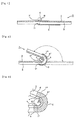
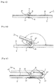
- Figs. 1 to 6 are conceptual illustrations for describing the opto-electric hybrid board of the present invention.
- the opto-electric hybrid board 1 of the present invention has, as shown in Fig.
- the opto-electric hybrid board of the present invention is applied to an electronic device having such a structure that a part of the opto-electric hybrid board is movable in a rotation direction with a hinge 4 as center, as shown in Fig. 2 .
- the reinforcing member 5 disposed on the part on the side of the optical waveguide film to be bent, and the part to be bent in the present invention (which will be referred to as a "bent part” hereinafter) includes a part that is in contact with a hinge and an outer peripheral part thereof in the state where the opto-electric hybrid board is bent. Specifically, as shown in Fig.
- the bent part includes a part surrounded by the bend starting point X 1 where the circuit board starts to be bent with the hinge in contact therewith, the bend ending point X 2 where the bending ends, and the points Y 1 and Y 2 on the side of the optical waveguide film corresponding to X 1 and X 2 , respectively, and also includes a part 6 expanded outward therefrom, i.e., a part surrounded by the points a, b, c and d.
- the distance between points a and X 1 in the expanded part is not particularly limited within the range where the advantages of the present invention are obtained, and may be approximately from 1 to 10% of the distance between the points X 1 and X 2 .
- the position where the reinforcing member 5 is disposed in the present invention is on the side of the optical waveguide film of the bent part 6 surrounded by the points a, b, c and d of the opto-electric hybrid board 1, and the reinforcing member 5 provided at least at part of the region imports significantly high bending durability thereto.
- the optical waveguide film 3 disposed on the outer peripheral side in Fig. 3 receives the maximum value of the bending stress on the outermost peripheral side, i.e., on the surface of the optical waveguide film 3, and in order to reduce the bending radius R, it is necessary to reduce the elastic modulus of the waveguide for facilitating the bending operation.
- reduction of the elastic modulus generally decreases the tensile strength, and therefore, in the case where the bending radius R is small, the optical waveguide film suffers shortage of the strength on the surface thereof to cause cracks, which bring about breakage thereof.
- the reinforcing member 5 is disposed on the surface of the optical waveguide film where the bending stress becomes maximum, whereby the bending strength against the maximum stress occurred on the surface is shared by the reinforcing member, and thus cracks are prevented from occurring in the film waveguide having low elastic modulus even in the state where the bending radius R is small. Furthermore, it has also been found that when the thickness of the reinforcing member 5 is increased, such a strength can be provided that resists the bending stress occurring inside within the thickness from the surface.
- Figs. 1 and 2 show an example of the opto-electric hybrid board of the present invention, which is an example where the reinforcing member 5 is disposed on the side of the optical waveguide film of the opto-electric hybrid board over the entire bent part 6.
- the reinforcing member 5 may be provided over the entire bent part 6 or may be provided on only a part thereof.
- the reinforcing number 5 may not be necessarily provided over the entire bent part unless the advantages of the present invention cannot be obtained.
- the part on the side of the optical waveguide film Y 1 corresponding to the bend starting point X 1 is particularly preferably reinforced, and for example, as shown in Figs. 4 and 5 , the reinforcing member 5 may be disposed only on a part covering the part Y 1 , thereby imparting high bending durability.
- Fig. 6 shows an example where an electronic device has a sliding mechanism.
- the opto-electric hybrid board 1 is bent with the bent part as center, and in this state, for example, the straight portions of the flexible opto-electric hybrid board disposed on the upper side and the lower side respectively arse substantially in parallel to each other, While maintaining the bent state, at least one end part X 0 of the opto-electric hybrid board 1 is moved (in the rightward direction in Fig. 6 ), and the bent part is also moved associated with the movement of the end part. Accordingly, the bend starting point is moved associated with the movement of the end part X 0 .
- the range, within which the bend starting point is moved is preferably reinforced with the reinforcing member 5. Specifically, as shown in Fig.
- the part (Y 1 to Y 3 ) on the side of the optical waveguide film within the range of from the move starting point (X 1 ) in the horizontal direction of the bent part 6 to the move ending point (X 3 ) thereof is preferably reinforced.
- the bent part means a part that is in contact with the bending shaft and an outer peripheral part thereof, and thus the definition thereof is the same as the aforementioned description of the bent part provided that the hinge 4 is replaced by the bending shaft 7.
- the bending shaft may be actually provided, whereby the sliding mechanism is achieved by moving the bending shaft 7 in the horizontal direction with or without rotation.
- the bending shaft 7 may not be actually provided, and the sliding structure is achieved by holding the opto-electric hybrid board 1 with lid members and the like from above and below, and moving the end part X 0 of the opto-electric hybrid board 1 in the horizontal direction through the movement of the lid members.
- the opposite end of the opto-electric hybrid board is generally fixed, but may have such a structure that the opposite end is moved in the opposite direction to the end part X 0 .
- the material used as the reinforcing member 5 is not particularly limited as far as the advantages of the present invention can be obtained, and a material having a tensile strength that is larger than that of the optical waveguide film is preferably used from the standpoint of effective exhibition of the bending durability. More specifically, the reinforcing member preferably has a tensile strength three times or more, more preferably a strength five times or more, and particularly preferably a strength eight times or more, greater than the tensile strength of the optical waveguide film.
- the tensile strength referred herein does not depend on the measurement method therefor, but what is important is the relative values between the reinforcing material and the optical waveguide film, and is generally measured according to JIS K7127.
- the material used as the reinforcing member include a polyimide resin used as a substrate of a flexible electric circuit board, and also include an aramid resin, a glass fiber-reinforced resin and a carbon fiber-reinforced resin, and among these, a polyimide resin and an aramid resin are preferred from the standpoint of exhibition of the advantages of the present invention. These resins may be used solely or as a combination of two or more of them.
- the thickness of the reinforcing member is not particularly limited within the range where the advantages of the present invention are exhibited, and the ratio to the thickness of the substrate constituting the flexible electric circuit board (reinforcing member/flexible electric circuit boared) is preferably in a range of from 4/1 to 1/4.
- the thickness of the reinforcing member is preferably relatively small for suppressing the optical loss, and the thickness of the reinforcing member is preferably relatively large for achieving the bending durability.
- the ratio in thickness of the reinforcing member and the flexible electric circuit board is preferably in a range of from 1/1 to 1/4, and particularly preferably in a range of from 1/1 to 1/2.
- the thickness of the reinforcing member is preferably in a range of from 4 to 50 ⁇ m, and for suppressing the optical loss, is more preferably in a range of from 4 to 25 ⁇ m, and particularly preferable in a range of from 4 to 15 ⁇ m.
- optical waveguide film and the flexible electric circuit board used in the present invention will be explained below.
- the optical waveguide film of the present invention has a core and a clad, and those having been used as an optical waveguide film can be used.
- a resin film for forming an optical waveguide formed of a resin composition containing (A) a base polymer, (B) a photopolymerizable compound and (C) a photopolymerization initiator can be used.
- the base polymer (A) is used for ensuring strength of the cured product, and is not particularly limited as far as the object thereof is attained, and examples thereof include a phenoxy resin, an epoxy resin, a (meth)acrylic resin, a polycarbonate resin, a polyallylate resin, polyetheramide, polyetherimide, polyethersulfone and derivatives thereof.
- the base polymer may be used solely or as a mixture of two or more thereof.
- the photopolymerizable compound (B) is not particularly limited as far as it is polymerized by irradiation with light, such as an ultraviolet ray, and is preferably a compound having an ethylenically unsaturated group in the molecule thereof from the standpoint of reactivity with light. Specific examples thereof include (meth)acrylate, vinylidene halide, vinyl ether, vinylpyridin and vinylphenol, and among these, (meth)acrylate is preferred from the standpoint of transparency and heat resistance. Any of a monofunctional compound, a bifunctional compound and a trifunctional compound can be used as the (meth)acrylate.
- the term (meth)acrylate herein means acrylate and methacrylate.
- the photopolymerization initiator (C) is not particularly limited, and examples thereof include an aromatic ketone, such as benzophenone, N.N'-tetramethyl-4,4'-diaminobenzophenone (Michler's ketone), N,N'-tetraethyl-4,4'-diaminobenzophenone, 4-methoxy-4'-dimethylaminobenzophenone, 2-benzyl-2-dimethylamino-1-(4-morpholinophenyl)-butan-1-one, 2,2-dimethoxy-1,2-diphenylethan-1-one, 1-hydroxycyclohexyl phenyl ketone, 2-hydroxy-2-methyl-1-phenylpropan-1-one, 1- (4- (2-hydroxyethoxy)phenyl)-2-hydroxy-2-methyl-1-propan-1-one and 1,2-methyl-1-(4- (methylthio)phenyl) -2-morpholinopropan-1-one; a quinone
- the amount of the base polymer (A) used is preferably from 10 to 80% by mass based on the total amount of the component (A) and the component (B). In the case where the amount is 10% by mass or more, a thick film having a thickness of 50 ⁇ m or more can be easily produced upon forming a film, In the case where the amount is 80% by mass or less, on the other hand, the photocuring reaction can sufficiently proceed. Taking these factors into consideration, the amount of the base polymer (A) used is more preferably from 20 to 70% by mass.
- the amount of the photopolymerizable compound (B) used is preferably from 20 to 90% by mass based on the total amount of the component (A) and the component (B). In the case where the amount is 20% by mass or more, the base polymer can be easily entwined therein and cured. In the case where the amount is 90% by mass or less, on the other hand, a film having a large thickness can be easily formed. Taking these factors into consideration, the amount of the photopolymerizable compound (B) used is more preferably from 30 to 80% by mass.
- the amount of the photopolymerization initiator (C) used is preferably from 0.1 to 10 parts by mass per 100 parts by mass of the component (A) and the component (B). In the case where the amount is 0.1 parts by mass or more, sufficient optical sensitivity can be obtained. In the case where the amount is 10% by mass or less, absorption on the surface layer of the photosensitive resin composition is prevented from becoming too large in exposure, and photocuring of the interior thereof can proceed sufficiently. Furthermore, transmission loss due to light absorption of the photopolymerization initiator itself can be favorably prevented from becoming larger. Taking these factors into consideration, the amount of the photopolymerization initiator (C) used is more preferably from 0.2 to 5% by mass.
- the optical waveguide film of the present invention can be easily produced by coating a resin composition containing the components (A) to (C) dissolved in a solvent on a substrate, followed by removing the solvent.
- the solvent used herein is not particularly limited as far as it can dissolve the resin composition, and examples thereof include such solvents as acetone, methyl ethyl ketone, methyl cellosolve, ethyl cellosolve, toluene, N,N-dimethylformamide, N,N-dimethylacetamide and propylene glycol monomethyl ether, and mixed solvents of them.
- the solid concentration in the resin solution is generally preferably approximately from 30 to 60% by mass.
- the thickness of the optical waveguide film of the present invention is not particularly limited, and the thickness after drying is generally from 10 to 250 ⁇ m, In the case where the thickness is 10 ⁇ m or more, such an advantage is obtained that the coupling tolerance with a light receiving-emitting device and an optical fiber can be enhanced, and in the case where the thickness is 250 ⁇ m or less, such an advantage is obtained that the coupling efficiency with a light receiving-emitting device and an optical fiber can be improved. Taking these factors into consideration, the thickness of the film is more preferably in a range of from 40 to 90 ⁇ m.
- the substrate used in the production process of the resin film for forming an optical waveguide in the present invention is a supporting substrate that supports the film for forming an optical waveguide, and is not particularly limited in material, and preferred examples thereof include polyester, such as polyethylene terephthalate, polypropylene and polyethylene since the film for forming an optical waveguide can be easily released therefrom later, and they have heat resistance and solvent resistance.
- the thickness of the substrate is preferably in a range of from 5 to 50 ⁇ m.
- the thickness of the substrate is more preferably in a range of from 10 to 40 ⁇ m, and more preferably from 20 to 30 ⁇ m.
- the film for forming an optical waveguide thus produced on the substrate can be easily stormed, for example, by winding in a roll form.
- a protective film may be provided on the film for forming an optical waveguide depending on necessity. The substrate and the protective film may be subjected to an antistatic treatment or the like for facilitating release of the film for forming an optical waveguide in a later stage.
- a production method for forming an optical waveguide by using the resin film for forming an optical waveguide obtained in the aforementioned manner will be described.
- the method include a method, in which a lower clad film released from the substrate is laminated under pressure with heating onto a board after removing the protective film in the case where the protective film is present.
- the lamination is preferably performed under reduced pressure from the standpoint of adhesiveness and followability.
- the heating temperature of the resin film is preferably from 50 to 130°C, and the pressing pressure therefor is preferably approximately from 0.1 to 1.0 MPa (approximately from 1 to 10 kgf/cm 2 ), although these conditions are not particularly limited.
- the thickness of the lower clad layer is not particularly limited and is preferably from 2 to 50 ⁇ m, In the case where the thickness is 2 ⁇ m or more, transmitted light can be easily confined inside the core, and in the case where the thickness is 50 ⁇ m or less, the total thickness of the optical waveguide may not become too large.
- the thickness of the lower clad layer is more preferably in a range of from 2 to 20 ⁇ m, and particularly preferably in a range of from 5 to 15 ⁇ m.
- the thickness of the lower clad layer herein is a value of from the interface between the core part and the lower clad layer to the lower surface of the lower clad layer.
- the lower clad film is cured with light or heat, and a core film having a higher refractive index than the lower clad film is laminated in the similar manner.
- the resin film thus laminated is irradiated with active light imagewise through a negative or positive mask pattern, which is referred to as an art work.
- a light source of the active light include known light source capable of radiating effectively an ultraviolet ray, such as a carbon arc lamp, a mercury vapor arc lamp, a superhigh pressure mercury lamp, a high pressure mercury lamp and a xenon lamp.
- those capable of radiating effectively visible light such as a photoflood lamp and a solar light lamp, may also be used.
- the height of the core part 2 is not particularly limited and is preferably from 10 to 150 ⁇ m. In the case where the height of the core part is 10 ⁇ m or more, the alignment tolerance on coupling with a light receiving-emitting device or an optical fiber after forming the optical waveguide can be prevented from being reduced, and in the case where the height is 150 ⁇ m or less, the coupling efficiency can be prevented from being reduced on coupling with a light receiving-emitting device or an optical fiber after forming the optical waveguide. In the present invention, for satisfying bending durability under a particularly small bending radius, the height of the core part is preferably in a range of from 30 to 120 ⁇ m, and particularly preferably in a range of from 50 to 90 ⁇ m.
- the non-exposed part is removed through development by wet development, dry development or the like, thereby producing the core pattern.
- the development is performed by using a developing liquid corresponding to the composition of the resin film, such as an organic solvent, an alkaline aqueous solution or an aqueous developing liquid, by a known method, such as spraying, immersion under oscillation, brushing and scraping.
- the developing liquid used is preferably ones that are safe and stable and are excellent in handleability, such as an organic solvent and an alkaline aqueous solution.
- organic solvent developing liquid examples include 1,1,1-trichloroethane, N-methylpyrrolidone, N,N-dimethylformamide, N,N-dimethylacetamide, cyclohexanone, methyl isobutyl ketone and ⁇ -butyrolactone.
- the organic solvent may contain water added in a range of from 1 to 20% by mass for preventing ignition.
- Examples of the base used in the alkaline aqueous solution include an alkalihydroxide, such as hydroxides of lithium, sodium and potassium, a carbonate alkali, such as carbonates and bicarbonates of lithium, sodium, potassium and ammonium, an alkali metal phosphate, such as potassium phosphate and sodium phosphate, and an alkali metal pyrophosphate, such as sodium pyrophosphate and potassium pyrophosphate.
- an alkalihydroxide such as hydroxides of lithium, sodium and potassium
- a carbonate alkali such as carbonates and bicarbonates of lithium, sodium, potassium and ammonium
- an alkali metal phosphate such as potassium phosphate and sodium phosphate
- an alkali metal pyrophosphate such as sodium pyrophosphate and potassium pyrophosphate.
- the alkaline aqueous solution used for development include a 0.1 to 5% by mass diluted solution of sodium carbonate, a 0.1 to 5% by mass diluted solution of potassium carbonate, a 0.1 to 5% by mass diluted solution of sodium hydroxide, and a 0.1 to 5% by mass diluted solution of sodium tetraborate.
- the alkaline aqueous solution used for development preferably has pH in a range of from 9 to 14, and the temperature thereof is controlled depending on the developing property of the layer of the photosensitive resin composition.
- the alkali aqueous solution may contain a surfactant, a defoaming agent and a small amount of an organic solvent for accelerating development.
- the aqueous developing liquid may contain water or an alkali aqueous solution and at least one organic solvent.
- the alkaline substance include, in addition to the aforementioned substances, borax, sodium metasilicate, tetramethylammonium hydroxide, ethanolamine, ethylenediamine, diethylenetriamine, 2-mini-2-hydraxymethyl-1,3-propanediol, 1,3-diaminopropanol-2-morpholine.
- the pH of the developing liquid is preferably as small as possible within a range capable of developing the resist sufficiently, and is preferably pH 8 to 12, and more preferably pH 9 to 10.
- organic solvent examples include triacetone alcohol, acetone, ethyl acetate, alkoxyethanol having an alkoxy group having from 1 to 4 carbon atoms, ethyl alcohol, isopropyl alcohol, butyl alcohol, diethylene glycol monomethyl ether, diethylene glycol monoethyl ether and diethylene glycol monobutyl ether. These may be used solely or in combination of two or more of them.
- concentration of the organic solvent is generally preferably from 2 to 90% by mass, and the temperature thereof can be controlled depending on the developing property.
- the aqueous developing liquid may contain a surfactant, a defoaming agent and the like added in a small amount.
- the developing method examples include a dipping method, a battle method, a spray method, such as a high pressure spray method, brushing and scraping.
- the core pattern may further be cured by heating to from 60 to 250°C or by exposing to from 0.1 to 1,000 mJ/cm 2 .
- an upper clad film having a lower refractive index than that of the core film is laminated thereon in the similar manner to produce an optical waveguide.
- the thickness of the upper clad layer is not particularly limited as far as it is in a range capable of embedding the core part, and is preferably from 2 to 50 ⁇ m after drying, For satisfying bending durability under a particularly small bending radius, the thickness is more Preferably in a range of from 2 to 20 ⁇ m, and particularly preferably in a range of from 5 to 15 ⁇ m.
- the thickness of the upper clad layer may be the same as or different from a thickness of the lower clad layer formed at the beginning.
- the thickness of the upper clad layer herein is a value from the boundary between the core part and the upper clad layer to the upper face of the upper clad layer.
- An FPC (flexible printed circuit) board can suitably be used as the flexible electric circuit board.
- the material for the FPC board may be polyimide, polyamide, polyetherimide, polyethylene terephthalate, a liquid crystal polymer and the like, and polyimide may be used from the standpoint of heat resistance and availability.
- Examples of a commercially available product thereof include an FPC board formed of Kapton (produced by Du Pont-Toray Co., Ltd.). While thickness of the board constituting the flexible electric circuit board is not particularly limited, the ratio in thickness of the reinforcing member and the board is preferably in a range of from 4/1 to 1/4 from the standpoint of bending durability as having been described above, and thus the thickness of the board is preferably selected to satisfy the range.
- the thickness of the board is also determined appropriately in consideration of the thickness that is demanded by the opto-electric hybrid board itself, and the thickness is preferably in a range of from 5 to 50 ⁇ m, more preferably in a range of from 5 to 25 ⁇ m, and particularly preferably in a range of from 5 to 15 ⁇ m.
- the opto-electric hybrid board of the present invention is produced by bonding the optical waveguide film and the flexible electric circuit board described above.
- an adhesive may be used depending on necessity.
- the kind of the adhesive can suitably be selected according to the materials of the optical waveguide film and the flexible electric circuit board.
- the adhesive preferably has flexibility after curing in order to provide the opto-electric hybrid board with flexibility, and specifically, the adhesive preferably has an elastic modulus of 700 MPa or less, more preferably 600 MPa or less, and particularly preferably 500 MPa or less, after curing.
- the elastic modulus is preferably 1 MPa or more, and more preferably 5 MPa or more, from the standpoint of the strength of the adhesive.
- Preferred examples of the kind of the adhesive include an acryl rubber base adhesive and, as a commercially available product, a high heat resistant adhesive insulating material KS7003 (elastic modulus: 700 MPa), produced by Hitachi Chemical Co., Ltd., an adhesive for a flexible printed circuit board Hi-Bon 808 (elastic modules: 50 MPa), produced by Hitachi Kasei polymer Co., Ltd. and the like.
- KS7003 elastic modulus: 700 MPa
- Hi-Bon 808 adhesive for a flexible printed circuit board Hi-Bon 808 (elastic modules: 50 MPa), produced by Hitachi Kasei polymer Co., Ltd. and the like.
- the bonding method of the optical waveguide film and the flexible electric circuit board is not particularly limited, and such methods are preferred as a method using a roll laminator and a method using a flat plate laminator from the standpoint of the adhesion property and prevention of entrainment of air bubbles.
- the lamination temperature of the roll laminator is preferably in a range of from room temperature (25°C) to 100°C. In the case where the temperature is room temperature (25°C) or more, the adhesive property to the optical waveguide is enhanced, and in the case where the temperature is 100°C or less, on the other hand, the adhesive layer is prevented from flowing, thereby providing the required thickness. Taking these factors into consideration, the temperature is more preferably in a range of from 40 to 100°C.
- the pressure is preferably from 0.2 to 1.0 MPa (from 1 to 10 kgf/cm 2 ), and the lamination speed is preferably from 0.1 to 3 m/min.
- the flat plate laminator herein means a laminator, in which materials to be laminated are held between a pair of flat plates and press-adhered by applying pressure to the flat plates, and a vacuum pressure laminator can be preferably used.
- the heating temperature thereon is preferably from 50 to 100°C, and the pressing pressure is preferably from 0.1 to 1.0 MPa (from 1 to 10 kgf/cm 2 ).
- these conditions are not particularly limited.
- the reinforcing member which is one of the features of the present invention, is attached to the opto-electric hybrid board thus produced in the aforementioned manner.
- the method for attaching the reinforcing member is not particularly limited, and a method using an adhesive may be conveniently employed.
- Examples of the adhesive used herein include the same ones as being used for bonding the optical waveguide film and the flexible electric circuit board.
- a specimen having a width of 10 mm and a length of 70 mm was obtained from the film to be measured, and was measured according to JIS K7127 under the following conditions with a tensile tester (RTM-100, produced by Orientec Co., Ltd.). Conditions: distance between chucks: 50 mm; temperature: 25°C; tensile speed: 50 mm/min
- the tensile elastic modulus was calculated by the following expression from the initial straight line part of the tensile stress-distortion curve. The maximum strength until breakage in the tensile stress-distortion curve was designated as the tensile strength.
- Tensile elastic modulus (MPa) (difference (N) in stress between two points on the straight line) / (original average cross-sectional area (mm 2 ) of optical waveguide film) / (difference in distortion between the two points)
- the opto-electric hybrid boards produced in Examples and Comparative Examples were subjected to a bending durability test under the conditions of a bending angle of from 0 to 180° a bending radius of 1.5 mm and a bending speed of 2 per second with a bending durability tester produced by Daisho Denshi Co., Ltd.), and the presence of breakage was observed every 100,000 times bending, thereby measuring the maximum number of bending until breakage.
- the bending durability test used for evaluating the transmission loss of light and the appearance of the core described below was performed for two or more specimens with a time difference therehetween, and the number of bending that was smaller by 10% than the number of bending when the specimen having been subjected to the test most precedently was broken was designated as the number immediately before breakage.
- the opto-electric hybrid boards produced in Examples and Comparative Examples were measured for transmission loss before bending and transmission loss after bending in the number immediately before breakage in the bending durability test, and the transmission loss of light was evaluated by the difference therebetween.
- the opto-electric hybrid boards produced in Examples and Comparative Examples were visually evaluated for appearance of the core after bending in the number immediately before breakage in the bending durability test.
- the evaluation standard was as follows.
- the resin vanish was filtrated under pressure through Polyflon Filter (a trade name, PFQ20, produced by Advantech Toyo Co., Ltd.) having a pore diameter of 2 ⁇ m under the conditions of a temperature of 25°C and a pressure of 0.4 MPa, and was further defoamed under reduced pressure for 15 minutes with a vacuum pump and a bell jar under the condition of a vacuum degree of 50 mm Hg.
- Polyflon Filter a trade name, PFQ20, produced by Advantech Toyo Co., Ltd.
- the resin vanish A for forming a clad layer thus obtained was coated on a corona-treated surface of a polyamide film (Mictron, a trade name, produced by Tory Industries, Inc., thickness: 12 ⁇ m) with a coating machine (Multicoater TM-MC, produced by Hirano Tecseed Co., Ltd.), and was dried at 80°C for 10 minutes and then at 100°C for 10 minutes.
- a releasable PET film (Purex A31, a trade name, produced by Teijin DuPont Films Japan Ltd., thickness; 25 ⁇ m) as a protective film was attached thereon with the releasable surface facing the resin side, thereby preparing a resin film for forming a clad layer.
- the thickness of the resin layer may be arbitrarily controlled by controlling the gap of the coating machine.
- the gap was controlled to make the film thicknesses after curing of 20 ⁇ m for the lower clad layer and 70 ⁇ m for the upper clad layer.
- a resin vanish B for forming a core layer was prepared in the same manner under the same conditions as in the production example of the resin film for forming a clad layer described above, except that 26 parts by mass of a phenoxy resin (Phenotohto YP-70, a trade name, produced by Tohto Kasei Co., Ltd.) as the binder polymer (A), 36 parts by mass of 9,9-bis(4-(2-acryloyloxyethoxy)phenyl)fluorene (A-BPEF, a trade name, produced by Shin-Nakamura Chemical Co., Ltd.) and 36 parts by mass of a bisphenol A type epoxy acrylate (EA-1020, a trade name, produced by Shin-Nakamura Chemical Co., Ltd.) as the photopolymerizable compound (B), 1 part by mass of bis(2,4,6-trimethylbenzoyl)phenylphosphine oxide (Irgacure 819, a trade name, produced by Ciba
- the resin vanish B for forming a core layer obtained above was coated on a non-treated surface of a PET film (COSMO SHINE A1517, a trade name, produced by Toyobo Co., Ltd., thickness: 16 ⁇ m) and dried in the same manner as in the production example described above.
- COSMO SHINE A1517 a trade name, produced by Toyobo Co., Ltd., thickness: 16 ⁇ m
- a releasable PET film (Purex A31, a trade name, produced by Teijin DuPont Films Japan Ltd., thickness: 25 ⁇ m) as a protective film was attached thereon with the releasable surface facing the resin side, thereby preparing a resin film for forming a core layer.
- the gap of the coating machine was controlled to make the film thickness after curing of 50 ⁇ m.
- the releasable PET film (Purex A31) as the protective film of the resin film for forming a lower clad layer obtained above was peeled off, and the resin film was irradiated with an ultraviolet ray (wavelength: 365 nm) at 1 J/cm 2 from the resin side (the opposite side to the substrate film) with an ultraviolet ray exposing machine (EXM-1172, produced by Orc Manufacturing Co., Lid.), and then heat-treated at 80°C for 10 minutes, thereby producing a lower clad layer.
- an ultraviolet ray wavelength: 365 nm
- the resin film for forming a core layer described above was then laminated on the lower clad layer under the conditions of a pressure of 0.4 MPa, a temperature of 50°C and a laminating speed of 0.2 m/min with a roll laminator (HLM-1500, produced by Hitachi Plant Techno Co., Ltd.), and then the assembly was depressurized to 500 Pa or lower, and was pressed with heating under the conditions of a pressure of 0.4 MPa, a temperature of 50°C and a pressing time of 30 seconds, with a vacuum press laminator (MVLP-500, produced by Meiki Co., Ltd.) as a flat plate type laminator, thereby forming a core layer.
- HLM-1500 roll laminator
- the resin film for forming a clad layer described above was then laminated thereon as an upper clad layer under the same laminating conditions as described above. Furthermore, both surfaces thereof were irradiated with an ultraviolet ray (wavelength: 365 nm) at 25 J/cm 2 in total, and then the resin film was heat-treated at 160°C for 1 hour, thereby producing an upper clad layer, whereby a flexible optical waveguide having the substrate film disposed outside was produced.
- the flexible optical waveguide was treated under a high temperature and high humidity condition of 85°C/85% for 24 hours for peeling the polyamide film off, thereby producing an optical waveguide, from which the substrate film had been removed.
- the core layer and the clad layer were measured for refractive index with a prism coupler (Model 2010), produced by Metricon Inc., and the refractive index was 1.584 for the core layer and 1.550 for the clad layer at a wavelength of 830 nm.
- the tensile elastic modulus and the tensile strength of the optical waveguide film obtained were measured by the methods described above.
- the tensile elastic modulus was 2,000 MPa, and the tensile strength was 70 MPa.
- HTR-860P-3 (a trade name, produced by Teikoku Chemical Industry Co., Ltd., glycidyl group-containing acryl rubber, molecular weight: 1,000,000, Tg: -7°C), 5.4 parts by mass of YDCN-703 (a trade name, produced by Tohto Kasei Co., Ltd., o-cresol novolak type epoxy resin, epoxy equivalent: 210), 16.2 parts by mass of YDCN-8170C (a trade name, produced by Tohto Kasei Co., Ltd., bisphenol F type epoxy resin, epoxy equivalent: 157), 15.3 parts by mass of Plyophen LF2882 (a trade name, produced by Dainippon Ink & Chemicals Inc., bisphenol A novolak resin), 0.1 part by mass of NUCA-189 (a trade name, produced by Nippon Unicar Co., Ltd., ⁇ -mercaptopropyltrimethoxysilane), 0.3 part by mass of NUCA-1160 (a trade name,
- ⁇ -ureidopropyltriethoxysilane parts by mass of A-DPH (a trade name, produced by Shin-Nakamura Chemical Co. , Ltd. , dipentaerythritol hexaacrylate), 1.5 part by mass of Irgacure 369 (a trade name, 2-benzyl-2-dimethylamino-1-(4-morpholinophenyl)butanon-l-one, I-369, produced by Ciba Specialty chemicals Co., Ltd.) and cyclohexanone were mixed under stirring, and the mixture was deaerated under vacuum.
- A-DPH a trade name, produced by Shin-Nakamura Chemical Co. , Ltd. , dipentaerythritol hexaacrylate
- Irgacure 369 a trade name, 2-benzyl-2-dimethylamino-1-(4-morpholinophenyl)butanon-l-one, I-369, produced by Cib
- the adhesive vanish thus obtained was coated on a surface release-treated polyethylene terephthalate having a thickness of 75 ⁇ m (Teijin Tetron film A-31, produced by Teijin Limited), and dried by heating to 80°C for 30 minutes, thereby preparing- a tacky adhesive sheet.
- a light transmitting supporting substate having a thickness of 80 ⁇ m FHF-100, produced by Thermo Co., Ltd., a three-layer film of low density polyethylene terephthalate/vinyl acetate/low density polyethylene terephthalate
- the thickness of the tacky adhesive layer was 10 ⁇ m.
- the tacky adhesive layer of the sheet adhesive thus prepared was cured at 160°C for 1 hour, and the light transmittance thereof was measured with U-3310 ultraviolet/visible ray spectrophotometer, produced by Hitachi High-Technologies Corporation. As a result, a high transmittance of 98% or more at a wavelength of 850 nm was obtained, and the transmission loss was equivalent to 0.1 dB or less.
- the refractive index was measured with a prism coupler (Model 2010), produced by Metricon Inc., and the refractive index was 1.505 at a wavelength of 830 nm.
- the tensile elastic modulus of the sheet adhesive thus obtained was measured by the method described above, and the tensile elastic modulus was 350 MPa.
- the waveguide was cut into a strip form (length: 120 mm, width: 2 mm) with a dicing saw (DAD-341, produced by DISCO Corporation) and irradiated with an ultraviolet ray (365 nm) from the side of the supporting substrate to decrease the adhesive strength between the tacky adhesive layer and the supporting substrate, followed by peeling the supporting substrate, thereby providing an optical waveguide having an adhesive layer.
- a dicing saw DAD-341, produced by DISCO Corporation
- the optical waveguide having an adhesive layer was aligned to the prescribed position of a flexible electric circuit board having electric wiring (length: 120 mm, width: 2 mm, substrate: Kapton 100EN (having a tensile strength of 370 MPa measured by the method described above), thickness: 25 ⁇ m, copper circuit thickness: 12 ⁇ m) by utilizing the mask aligner mechanism of an ultraviolet ray exposing equipment (MAP-1200-L, produced by Dainippon Screen Mfg.
- MAP-1200-L ultraviolet ray exposing equipment
- the optical waveguide was temporarily adhered thereon by pressing under the conditions of a pressure of 0.4 MPa, a temperature of 80°C and a laminating speed of 0.2 m/minute with the roll laminator, and then heated in a clean oven to 160°C for hour to adhere the flexible optical waveguide to the electric circuit board, thereby producing an opto-electric hybrid board.
- the light transmittance of Kapton EN as the substrate of the flexible electric circuit board was measured with a spectrophotometer U-3310, produced by Hitachi High-Technologies Corporation, and the light transmittance was 86% at a wavelength of 850 nm.
- the value was equivalent to a transmission loss corresponding to 0.7 dB, and the optical loss through the electric circuit board derived from the total transmission loss of the substrate and the tacky adhesive layer was as low as less than 1 dB. Accordingly, a structure having no through-hole for light transmission provided was employed in this example.
- a reinforcing member was provided to cover the part Y 1 on the side of the optical waveguide film at the point X 1 where the opto-electric hybrid board was in contact with the hinge part (bend starting point).
- the reinforcing member used was a polyimide resin film (Kapton 50EN, produced by Du Pont-Toray Co., Ltd., thickness: 12.5 ⁇ m, tensile strength: 380 MPa) having a length of 30 mm and a width of 2 mm, which was the same as the electric circuit board.
- the results of evaluation in the manner described above are shown in Table 1.
- An opto-electric hybrid board was produced in the same manner as in Example 1 except that a flexible electric circuit board having a thickness of 12.5 ⁇ m (length: 120 mm, width: 2 mm) and having a substrate of Kapton 50EN (tensile strength: 380 MPa, copper circuit thickness; 12 ⁇ m) was used.
- the results of evaluation in the same manner as in Example 1 are shown in Table 1.
- An opto-electric hybrid board was produced in the same manner as in Example 2 except that the thickness of the reinforcing member was changed to 25 ⁇ m (Kapton 100EN, produced by Du Pont-Toray Co., Ltd., tensile strength: 370 MPa). The results of evaluation in the same manner as in Example 1 are shown in Table 1.
- An opto-electric hybrid board was produced in the same manner as in Example 2 except that an aramid resin film (Mictron ML, produced by Du Pont-Toray Co., Ltd., thickness: 25 ⁇ m, tensile strength: 600 MPa) was used as the reinforcing member.
- the results of evaluation in the same manner as in Example 1 are shown in Table 1.
- An opto-electric hybrid board was produced in the same manner as in Example 4 except that an aramid resin film having a thickness of 12.5 ⁇ m (Mictron ML, produced by Du Pont-Toray Co., Ltd., tensile strength: 600 MPa) was used as the reinforcing member.
- the results of evaluation in the same manner as in Example 1 are shown in Table 1.
- An opto-electric hybrid board was produced in the same manner as in Example 1 except that the reinforcing member was not provided.
- the results of evaluation in the same manner as in Example 1 are shown in Table 1.
- the opto-electric hybrid board is significantly enhanced in bending durability only by providing a reinforcing material on at least a part on the side of the optical waveguide film where the opto-electric hybrid board is in contact with the hinge, particularly on the bend starting point.
- the opto-electric hybrid board of the present invention has such excellent bending durability that the optical waveguide film part does not suffer breakage and cracking even when the circuit board is repeatedly bent over a prolonged period of time. Accordingly, the opto-electric hybrid board of the present invention can suitably be used for an electronic device, such as a mobile phone, and can maintain favorable communication function for a prolonged period of time even in the case where the circuit board is demanded to be bent at a hinge part with a small bending radius R of approximately from 1.5 to 2 mm, thereby achieving high reliability and durability of the electronic device itself.
Landscapes
- Physics & Mathematics (AREA)
- General Physics & Mathematics (AREA)
- Optics & Photonics (AREA)
- Engineering & Computer Science (AREA)
- Microelectronics & Electronic Packaging (AREA)
- Optical Integrated Circuits (AREA)
- Structure Of Printed Boards (AREA)
Abstract
A flexible opto-electric hybrid board containing an optical waveguide film containing a core and a clad, and a flexible electric circuit board bonded to each other, the flexible opto-electric circuit board further having a reinforcing member disposed on at least a part on a side of the optical waveguide film to be bent, and an electronic device containing the flexible opto-electric hybrid board.
Such an opto-electric hybrid board having an optical waveguide film and a flexible electric circuit board bonded to each other is provided that does not suffer breakage or cracks even when the circuit board is bent or folded, and an electronic device containing the opto-electric hybrid board is also provided.
Description
- The present invention relates to an opto-electric hybrid board with flexibility having optical wiring and electrical wiring combined, and an electronic device containing the circuit board.
- In recent years, the high-speed and high-density signal transmission among electronic devices and among circuit boards is encountering limitation in increase of the speed and density thereof due to barriers in transmission through conventional electric wiring, i.e., mutual interference and attenuation of signals. In order to break the limitation, a technique for connecting electronic devices and circuit boards by means of light, i.e., so-called optical interconnection, is being investigated. A polymer optical waveguide receives attention as an optical transmission path owing to easiness in processing, low cost, and high freedom and high density in wiring.
In particular, the use of an optical waveguide in a mobile phone, a notebook computer and the like is investigated, and an opto-electric hybrid board having optical wiring and electric wiring combined receives attention for space saving and reduction in thickness (see, for example,Patent Document 1,Fig. 2 ). - In an electronic device, such as a mobile phone, which is one of the application fields of an opt-electric hybrid board, it is assumed to use a flexible opto-electric hybrid board for signal transmission between two openable and closable mechanical units, and it is considered that the flexible opto-electric hybrid board bridges the two mechanical units through a connecting part (hinge). The flexible opto-electric hybrid board is generally bent to make the flexible electric circuit board into contact with the hinge, and the optical waveguide part may suffer breakage and cracks by bending in some cases. In particular, the circuit board is required to be bent at the hinge in a small bending radius R of from 1.5 to 2 mm associated with demand of reduction in size of electronic devices in recent years, thereby causing a problem in notable occurrence of breakage and cracks at the hinge.
- In order to solve the problem, such a flexible opto-electric circuit board has been proposed that an optical waveguide film and a flexible electric circuit board are partly bonded to each other, and are not bonded to each other at least a part where the circuit board is bent (see,
Patent Document 2, scope of claim).
Even in the aforementioned techniques, however, the optical waveguide part receives stress when the circuit board is actually bent at the hinge, thereby failing to solve the problem in occurrence of breakage and cracks. - Patent Document 1: Japanese Patent No.
3193500
Patent Document 2: Japanese Paten Application Laid-Open No.284925/2006 - The present invention has been made for solving the aforementioned problems, and an object thereof is to provide such an opto-electric hybrid board having an optical waveguide film and a flexible electric circuit board bonded to each other that does not suffer breakage or cracks even when the circuit board is bent or folded, and to provide an electronic device containing the opto-electric hybrid board.
- As a result of earnest investigations made by the present inventors, it has been found that an opto-electric hybrid board can be significantly enhanced in strength by disposing a reinforcing member in a position that receives stress upon bending at a hinge, thereby preventing breakage and cracks from occurring in the optical waveguide part. The present invention has been completed based on the finding.
Accordingly, the present invention provides a flexible opto-electric hybrid board comprising an optical waveguide film containing a core and a clad, and a flexible electric circuit board bonded to each other, the flexible opto-electric circuit board further having a reinforcing member disposed on at least a part on a side of the optical waveguide film to be bent, and also provides an electronic device containing the flexible opto-electric hybrid board. - The opto-electric hybrid board and the electronic devices containing the opto-electric hybrid board according to the present invention have such a good bending durability that the opto-electric hybrid board does not suffer breakage and cracking even after suffering repeated bending over a prolonged period of time and maintains good communication function.
-
-
Fig. 1 is a conceptual illustration showing an example of a flexible opto-electric hybrid board according to the present invention. -
Fig. 2 is a conceptual illustration of the flexible opto-electric hybrid board according to the present invention shown inFig. 1 in a bent state. -
Fig. 3 is an enlarged illustration of a hinge part inFig. 2 . -
Fig. 4 is a conceptual illustration showing another example of a flexible opto-electric hybrid board according to the present invention. -
Fig. 5 is a conceptual illustration of the flexible opto-electric hybrid board according to the present invention shown inFig. 4 in a bent state. -
Fig. 6 is a conceptual illustration showing an example of a flexible opto-electric hybrid board in the case where an electronic device has a sliding mechanism. -
- 1. Flexible opto-electric hybrid board
- 2. Flexible electric circuit board
- 3. Optical waveguide film
- 4. Hinge
- 5. Reinforcing member
- 6. Bent part
- 7. Bending shaft
- The opto-electric hybrid board of the present invention contains an optical waveguide containing a core and a clad, and a flexible electric circuit board bonded to each other, and a reinforcing member is disposed on at least a part on a side of the optical waveguide film to be bent. The present invention will be described in detail with reference to the drawings below.
Figs. 1 to 6 are conceptual illustrations for describing the opto-electric hybrid board of the present invention. The opto-electric hybrid board 1 of the present invention has, as shown inFig. 1 , anoptical waveguide film 3 having a core and a clad, and a flexibleelectric circuit board 2 bonded to each other, and a reinforcingmember 5 is disposed on a part on the side of the optical waveguide film to be bent. Taking the adhesiveness between theoptical waveguide film 3 and the flexibleelectric circuit board 2 into consideration, it is preferred that they are adhered over the entire surfaces.
The opto-electric hybrid board of the present invention is applied to an electronic device having such a structure that a part of the opto-electric hybrid board is movable in a rotation direction with ahinge 4 as center, as shown inFig. 2 . - One of the features of the opto-electric hybrid board of the present invention is, as described above, the reinforcing
member 5 disposed on the part on the side of the optical waveguide film to be bent, and the part to be bent in the present invention (which will be referred to as a "bent part" hereinafter) includes a part that is in contact with a hinge and an outer peripheral part thereof in the state where the opto-electric hybrid board is bent. Specifically, as shown inFig. 3 , which is an enlarged illustration of the hinge part, the bent part includes a part surrounded by the bend starting point X1 where the circuit board starts to be bent with the hinge in contact therewith, the bend ending point X2 where the bending ends, and the points Y1 and Y2 on the side of the optical waveguide film corresponding to X1 and X2, respectively, and also includes apart 6 expanded outward therefrom, i.e., a part surrounded by the points a, b, c and d. The distance between points a and X1 in the expanded part is not particularly limited within the range where the advantages of the present invention are obtained, and may be approximately from 1 to 10% of the distance between the points X1 and X2.
Accordingly, the position where the reinforcingmember 5 is disposed in the present invention is on the side of the optical waveguide film of thebent part 6 surrounded by the points a, b, c and d of the opto-electric hybrid board 1, and the reinforcingmember 5 provided at least at part of the region imports significantly high bending durability thereto. - More specifically, the
optical waveguide film 3 disposed on the outer peripheral side inFig. 3 receives the maximum value of the bending stress on the outermost peripheral side, i.e., on the surface of theoptical waveguide film 3, and in order to reduce the bending radius R, it is necessary to reduce the elastic modulus of the waveguide for facilitating the bending operation. However, reduction of the elastic modulus generally decreases the tensile strength, and therefore, in the case where the bending radius R is small, the optical waveguide film suffers shortage of the strength on the surface thereof to cause cracks, which bring about breakage thereof.
In the present invention, it has been found that the reinforcingmember 5 is disposed on the surface of the optical waveguide film where the bending stress becomes maximum, whereby the bending strength against the maximum stress occurred on the surface is shared by the reinforcing member, and thus cracks are prevented from occurring in the film waveguide having low elastic modulus even in the state where the bending radius R is small.
Furthermore, it has also been found that when the thickness of the reinforcingmember 5 is increased, such a strength can be provided that resists the bending stress occurring inside within the thickness from the surface. -
Figs. 1 and 2 show an example of the opto-electric hybrid board of the present invention, which is an example where the reinforcingmember 5 is disposed on the side of the optical waveguide film of the opto-electric hybrid board over theentire bent part 6. In this manner, the reinforcingmember 5 may be provided over theentire bent part 6 or may be provided on only a part thereof. In other words, the reinforcingnumber 5 may not be necessarily provided over the entire bent part unless the advantages of the present invention cannot be obtained.
In thebent part 6, the part on the side of the optical waveguide film Y1 corresponding to the bend starting point X1 is particularly preferably reinforced, and for example, as shown inFigs. 4 and 5 , the reinforcingmember 5 may be disposed only on a part covering the part Y1, thereby imparting high bending durability. -
Fig. 6 shows an example where an electronic device has a sliding mechanism. The opto-electric hybrid board 1 is bent with the bent part as center, and in this state, for example, the straight portions of the flexible opto-electric hybrid board disposed on the upper side and the lower side respectively arse substantially in parallel to each other, While maintaining the bent state, at least one end part X0 of the opto-electric hybrid board 1 is moved (in the rightward direction inFig. 6 ), and the bent part is also moved associated with the movement of the end part. Accordingly, the bend starting point is moved associated with the movement of the end part X0. In this case, the range, within which the bend starting point is moved, is preferably reinforced with the reinforcingmember 5. Specifically, as shown inFig. 6 , the part (Y1 to Y3) on the side of the optical waveguide film within the range of from the move starting point (X1) in the horizontal direction of thebent part 6 to the move ending point (X3) thereof is preferably reinforced.
In an electronic device having a sliding mechanism, in which the opto-electric hybrid board is bent, and a shaft 7 (which will be referred to as a "bending shaft" hereinafter) corresponding to thehinge 4 is assumed, as shown inFig. 6 , the bent part means a part that is in contact with the bending shaft and an outer peripheral part thereof, and thus the definition thereof is the same as the aforementioned description of the bent part provided that thehinge 4 is replaced by the bendingshaft 7. The bending shaft may be actually provided, whereby the sliding mechanism is achieved by moving the bendingshaft 7 in the horizontal direction with or without rotation. In alternative, the bendingshaft 7 may not be actually provided, and the sliding structure is achieved by holding the opto-electric hybrid board 1 with lid members and the like from above and below, and moving the end part X0 of the opto-electric hybrid board 1 in the horizontal direction through the movement of the lid members. The opposite end of the opto-electric hybrid board is generally fixed, but may have such a structure that the opposite end is moved in the opposite direction to the end part X0. - The material used as the reinforcing
member 5 is not particularly limited as far as the advantages of the present invention can be obtained, and a material having a tensile strength that is larger than that of the optical waveguide film is preferably used from the standpoint of effective exhibition of the bending durability. More specifically, the reinforcing member preferably has a tensile strength three times or more, more preferably a strength five times or more, and particularly preferably a strength eight times or more, greater than the tensile strength of the optical waveguide film. The tensile strength referred herein does not depend on the measurement method therefor, but what is important is the relative values between the reinforcing material and the optical waveguide film, and is generally measured according to JIS K7127. - Specific examples of the material used as the reinforcing member include a polyimide resin used as a substrate of a flexible electric circuit board, and also include an aramid resin, a glass fiber-reinforced resin and a carbon fiber-reinforced resin, and among these, a polyimide resin and an aramid resin are preferred from the standpoint of exhibition of the advantages of the present invention. These resins may be used solely or as a combination of two or more of them.
- The thickness of the reinforcing member is not particularly limited within the range where the advantages of the present invention are exhibited, and the ratio to the thickness of the substrate constituting the flexible electric circuit board (reinforcing member/flexible electric circuit boared) is preferably in a range of from 4/1 to 1/4. The thickness of the reinforcing member is preferably relatively small for suppressing the optical loss, and the thickness of the reinforcing member is preferably relatively large for achieving the bending durability. In order to attain both factors, the ratio in thickness of the reinforcing member and the flexible electric circuit board is preferably in a range of from 1/1 to 1/4, and particularly preferably in a range of from 1/1 to 1/2.
In consideration of practical installation in an electronic device, the thickness of the reinforcing member is preferably in a range of from 4 to 50 µm, and for suppressing the optical loss, is more preferably in a range of from 4 to 25 µm, and particularly preferable in a range of from 4 to 15 µm. - The optical waveguide film and the flexible electric circuit board used in the present invention will be explained below.
- The optical waveguide film of the present invention has a core and a clad, and those having been used as an optical waveguide film can be used. For example, a resin film for forming an optical waveguide formed of a resin composition containing (A) a base polymer, (B) a photopolymerizable compound and (C) a photopolymerization initiator can be used.
- In the case where a cured product, such as a film, is to be formed, the base polymer (A) is used for ensuring strength of the cured product, and is not particularly limited as far as the object thereof is attained, and examples thereof include a phenoxy resin, an epoxy resin, a (meth)acrylic resin, a polycarbonate resin, a polyallylate resin, polyetheramide, polyetherimide, polyethersulfone and derivatives thereof. The base polymer may be used solely or as a mixture of two or more thereof.
- The photopolymerizable compound (B) is not particularly limited as far as it is polymerized by irradiation with light, such as an ultraviolet ray, and is preferably a compound having an ethylenically unsaturated group in the molecule thereof from the standpoint of reactivity with light. Specific examples thereof include (meth)acrylate, vinylidene halide, vinyl ether, vinylpyridin and vinylphenol, and among these, (meth)acrylate is preferred from the standpoint of transparency and heat resistance. Any of a monofunctional compound, a bifunctional compound and a trifunctional compound can be used as the (meth)acrylate.
The term (meth)acrylate herein means acrylate and methacrylate. - The photopolymerization initiator (C) is not particularly limited, and examples thereof include an aromatic ketone, such as benzophenone, N.N'-tetramethyl-4,4'-diaminobenzophenone (Michler's ketone), N,N'-tetraethyl-4,4'-diaminobenzophenone, 4-methoxy-4'-dimethylaminobenzophenone, 2-benzyl-2-dimethylamino-1-(4-morpholinophenyl)-butan-1-one, 2,2-dimethoxy-1,2-diphenylethan-1-one, 1-hydroxycyclohexyl phenyl ketone, 2-hydroxy-2-methyl-1-phenylpropan-1-one, 1- (4- (2-hydroxyethoxy)phenyl)-2-hydroxy-2-methyl-1-propan-1-one and 1,2-methyl-1-(4- (methylthio)phenyl) -2-morpholinopropan-1-one; a quinone, such as 2-ethylanthraquinone, phenanthrenequinone, 2-tert-butylanthraquinone, octamethylanthraquinone, 1,2-benzanthraquinone, 2,3-benzanthraquinone, 2-phenylanthraquinome, 2,3-diphenylanthraquinone, 1-chloroanthraquinone, 2-methylanthraquinone, 1,4-naphthoquinone, 9,10-phenanthraquinone, 2-methyl-1,4-naphthoquinone and 2,3-dimethylanthraquinone; a benzoin ether compound, such as benzoin methyl ether, benzoin ethyl ether and benzoin phenol ether; a benzoin compound, such as benzoin, methylbenzoin and ethylbenzoin; a benzyl derivative, such as benzyl dimethyl ketal; a 2,4,5-triarylimidazole dimer, such as 2-(o-chlorophenyl)-4,5-diphenylimidazole dimer, 2-(o-chlorophenyl)-4,5-di(methoxyphenyl)imidazole dimer, 2-(o-fluorophenyl)-4-5-diphenylimidazole dimer, 2- (o-methoxyphenyl)-4,5-diphenylimidazole dimer and 2- (p-methoxyphenyl)-4,5-diphenylimidazole dimer; a phosphine oxide, such as bis(2,4,6-trimethylbenzoyl)phenylphosphine oxide, bis(2,6-dimethoxybenzoyl)-2,4,4-trimethylpentylphosphine oxide and 2,4,6-trimethylbenzoyldiphenylphosphine oxide; an acridine derivative, such as 9-phenylacridine and 1,7-bis(9,9'-acridinyl)heptane; N-phenylglycine; an N-phenylglycine derivative; and a coumarin compound.
- The amount of the base polymer (A) used is preferably from 10 to 80% by mass based on the total amount of the component (A) and the component (B). In the case where the amount is 10% by mass or more, a thick film having a thickness of 50 µm or more can be easily produced upon forming a film, In the case where the amount is 80% by mass or less, on the other hand, the photocuring reaction can sufficiently proceed. Taking these factors into consideration, the amount of the base polymer (A) used is more preferably from 20 to 70% by mass.
- The amount of the photopolymerizable compound (B) used is preferably from 20 to 90% by mass based on the total amount of the component (A) and the component (B). In the case where the amount is 20% by mass or more, the base polymer can be easily entwined therein and cured. In the case where the amount is 90% by mass or less, on the other hand, a film having a large thickness can be easily formed. Taking these factors into consideration, the amount of the photopolymerizable compound (B) used is more preferably from 30 to 80% by mass.
- The amount of the photopolymerization initiator (C) used is preferably from 0.1 to 10 parts by mass per 100 parts by mass of the component (A) and the component (B). In the case where the amount is 0.1 parts by mass or more, sufficient optical sensitivity can be obtained. In the case where the amount is 10% by mass or less, absorption on the surface layer of the photosensitive resin composition is prevented from becoming too large in exposure, and photocuring of the interior thereof can proceed sufficiently. Furthermore, transmission loss due to light absorption of the photopolymerization initiator itself can be favorably prevented from becoming larger. Taking these factors into consideration, the amount of the photopolymerization initiator (C) used is more preferably from 0.2 to 5% by mass.
- The optical waveguide film of the present invention can be easily produced by coating a resin composition containing the components (A) to (C) dissolved in a solvent on a substrate, followed by removing the solvent. The solvent used herein is not particularly limited as far as it can dissolve the resin composition, and examples thereof include such solvents as acetone, methyl ethyl ketone, methyl cellosolve, ethyl cellosolve, toluene, N,N-dimethylformamide, N,N-dimethylacetamide and propylene glycol monomethyl ether, and mixed solvents of them. The solid concentration in the resin solution is generally preferably approximately from 30 to 60% by mass.
- The thickness of the optical waveguide film of the present invention is not particularly limited, and the thickness after drying is generally from 10 to 250 µm, In the case where the thickness is 10 µm or more, such an advantage is obtained that the coupling tolerance with a light receiving-emitting device and an optical fiber can be enhanced, and in the case where the thickness is 250 µm or less, such an advantage is obtained that the coupling efficiency with a light receiving-emitting device and an optical fiber can be improved. Taking these factors into consideration, the thickness of the film is more preferably in a range of from 40 to 90 µm.
- The substrate used in the production process of the resin film for forming an optical waveguide in the present invention is a supporting substrate that supports the film for forming an optical waveguide, and is not particularly limited in material, and preferred examples thereof include polyester, such as polyethylene terephthalate, polypropylene and polyethylene since the film for forming an optical waveguide can be easily released therefrom later, and they have heat resistance and solvent resistance. The thickness of the substrate is preferably in a range of from 5 to 50 µm. In the case where the thickness is 5 µm or more, such an advantage is obtained that the strength as the supporting substrate can be easily obtained, and in the case where the thickness is 50 µm or less, such an advantage is obtained that the gap to the mask used in pattern formation can be decreased to facilitate formation of a finer pattern. Taking these factors into consideration, the thickness of the substrate is more preferably in a range of from 10 to 40 µm, and more preferably from 20 to 30 µm.
The film for forming an optical waveguide thus produced on the substrate can be easily stormed, for example, by winding in a roll form. Furthermore, a protective film may be provided on the film for forming an optical waveguide depending on necessity. The substrate and the protective film may be subjected to an antistatic treatment or the like for facilitating release of the film for forming an optical waveguide in a later stage. - A production method for forming an optical waveguide by using the resin film for forming an optical waveguide obtained in the aforementioned manner will be described. Examples of the method include a method, in which a lower clad film released from the substrate is laminated under pressure with heating onto a board after removing the protective film in the case where the protective film is present. The lamination is preferably performed under reduced pressure from the standpoint of adhesiveness and followability. The heating temperature of the resin film is preferably from 50 to 130°C, and the pressing pressure therefor is preferably approximately from 0.1 to 1.0 MPa (approximately from 1 to 10 kgf/cm2), although these conditions are not particularly limited.
- The thickness of the lower clad layer is not particularly limited and is preferably from 2 to 50 µm, In the case where the thickness is 2 µm or more, transmitted light can be easily confined inside the core, and in the case where the thickness is 50 µm or less, the total thickness of the optical waveguide may not become too large. In the present invention, for satisfying bending durability under a particularly small bending radius, the thickness of the lower clad layer is more preferably in a range of from 2 to 20 µm, and particularly preferably in a range of from 5 to 15 µm.
The thickness of the lower clad layer herein is a value of from the interface between the core part and the lower clad layer to the lower surface of the lower clad layer. - Subsequently, the lower clad film is cured with light or heat, and a core film having a higher refractive index than the lower clad film is laminated in the similar manner. The resin film thus laminated is irradiated with active light imagewise through a negative or positive mask pattern, which is referred to as an art work. Examples of a light source of the active light include known light source capable of radiating effectively an ultraviolet ray, such as a carbon arc lamp, a mercury vapor arc lamp, a superhigh pressure mercury lamp, a high pressure mercury lamp and a xenon lamp. Furthermore, those capable of radiating effectively visible light, such as a photoflood lamp and a solar light lamp, may also be used.
- The height of the
core part 2 is not particularly limited and is preferably from 10 to 150 µm. In the case where the height of the core part is 10 µm or more, the alignment tolerance on coupling with a light receiving-emitting device or an optical fiber after forming the optical waveguide can be prevented from being reduced, and in the case where the height is 150 µm or less, the coupling efficiency can be prevented from being reduced on coupling with a light receiving-emitting device or an optical fiber after forming the optical waveguide. In the present invention, for satisfying bending durability under a particularly small bending radius, the height of the core part is preferably in a range of from 30 to 120 µm, and particularly preferably in a range of from 50 to 90 µm. - Subsequently, after exposure, the non-exposed part is removed through development by wet development, dry development or the like, thereby producing the core pattern. In the case of the wet development, the development is performed by using a developing liquid corresponding to the composition of the resin film, such as an organic solvent, an alkaline aqueous solution or an aqueous developing liquid, by a known method, such as spraying, immersion under oscillation, brushing and scraping.
The developing liquid used is preferably ones that are safe and stable and are excellent in handleability, such as an organic solvent and an alkaline aqueous solution. Examples of the organic solvent developing liquid include 1,1,1-trichloroethane, N-methylpyrrolidone, N,N-dimethylformamide, N,N-dimethylacetamide, cyclohexanone, methyl isobutyl ketone and γ-butyrolactone. The organic solvent may contain water added in a range of from 1 to 20% by mass for preventing ignition. - Examples of the base used in the alkaline aqueous solution include an alkalihydroxide, such as hydroxides of lithium, sodium and potassium, a carbonate alkali, such as carbonates and bicarbonates of lithium, sodium, potassium and ammonium, an alkali metal phosphate, such as potassium phosphate and sodium phosphate, and an alkali metal pyrophosphate, such as sodium pyrophosphate and potassium pyrophosphate. Preferred examples of the alkaline aqueous solution used for development include a 0.1 to 5% by mass diluted solution of sodium carbonate, a 0.1 to 5% by mass diluted solution of potassium carbonate, a 0.1 to 5% by mass diluted solution of sodium hydroxide, and a 0.1 to 5% by mass diluted solution of sodium tetraborate. The alkaline aqueous solution used for development preferably has pH in a range of from 9 to 14, and the temperature thereof is controlled depending on the developing property of the layer of the photosensitive resin composition. The alkali aqueous solution may contain a surfactant, a defoaming agent and a small amount of an organic solvent for accelerating development.
- The aqueous developing liquid may contain water or an alkali aqueous solution and at least one organic solvent. Examples of the alkaline substance include, in addition to the aforementioned substances, borax, sodium metasilicate, tetramethylammonium hydroxide, ethanolamine, ethylenediamine, diethylenetriamine, 2-mini-2-hydraxymethyl-1,3-propanediol, 1,3-diaminopropanol-2-morpholine. The pH of the developing liquid is preferably as small as possible within a range capable of developing the resist sufficiently, and is preferably pH 8 to 12, and more preferably pH 9 to 10. Examples of the organic solvent include triacetone alcohol, acetone, ethyl acetate, alkoxyethanol having an alkoxy group having from 1 to 4 carbon atoms, ethyl alcohol, isopropyl alcohol, butyl alcohol, diethylene glycol monomethyl ether, diethylene glycol monoethyl ether and diethylene glycol monobutyl ether. These may be used solely or in combination of two or more of them. The concentration of the organic solvent is generally preferably from 2 to 90% by mass, and the temperature thereof can be controlled depending on the developing property. The aqueous developing liquid may contain a surfactant, a defoaming agent and the like added in a small amount.
- Furthermore, two or more kinds of the developing methods may be used in combination depending on necessity. Examples of the developing method include a dipping method, a battle method, a spray method, such as a high pressure spray method, brushing and scraping.
As a treatment after the development, the core pattern may further be cured by heating to from 60 to 250°C or by exposing to from 0.1 to 1,000 mJ/cm2. - Subsequently, an upper clad film having a lower refractive index than that of the core film is laminated thereon in the similar manner to produce an optical waveguide. The thickness of the upper clad layer is not particularly limited as far as it is in a range capable of embedding the core part, and is preferably from 2 to 50 µm after drying, For satisfying bending durability under a particularly small bending radius, the thickness is more Preferably in a range of from 2 to 20 µm, and particularly preferably in a range of from 5 to 15 µm. The thickness of the upper clad layer may be the same as or different from a thickness of the lower clad layer formed at the beginning. The thickness of the upper clad layer herein is a value from the boundary between the core part and the upper clad layer to the upper face of the upper clad layer.
- An FPC (flexible printed circuit) board can suitably be used as the flexible electric circuit board. The material for the FPC board may be polyimide, polyamide, polyetherimide, polyethylene terephthalate, a liquid crystal polymer and the like, and polyimide may be used from the standpoint of heat resistance and availability. Examples of a commercially available product thereof include an FPC board formed of Kapton (produced by Du Pont-Toray Co., Ltd.).
While thickness of the board constituting the flexible electric circuit board is not particularly limited, the ratio in thickness of the reinforcing member and the board is preferably in a range of from 4/1 to 1/4 from the standpoint of bending durability as having been described above, and thus the thickness of the board is preferably selected to satisfy the range. The thickness of the board is also determined appropriately in consideration of the thickness that is demanded by the opto-electric hybrid board itself, and the thickness is preferably in a range of from 5 to 50 µm, more preferably in a range of from 5 to 25 µm, and particularly preferably in a range of from 5 to 15 µm. - The opto-electric hybrid board of the present invention is produced by bonding the optical waveguide film and the flexible electric circuit board described above.
Upon bonding the optical waveguide film and the flexible electric circuit board, an adhesive may be used depending on necessity. The kind of the adhesive can suitably be selected according to the materials of the optical waveguide film and the flexible electric circuit board.
The adhesive preferably has flexibility after curing in order to provide the opto-electric hybrid board with flexibility, and specifically, the adhesive preferably has an elastic modulus of 700 MPa or less, more preferably 600 MPa or less, and particularly preferably 500 MPa or less, after curing. The elastic modulus is preferably 1 MPa or more, and more preferably 5 MPa or more, from the standpoint of the strength of the adhesive.
Preferred examples of the kind of the adhesive include an acryl rubber base adhesive and, as a commercially available product, a high heat resistant adhesive insulating material KS7003 (elastic modulus: 700 MPa), produced by Hitachi Chemical Co., Ltd., an adhesive for a flexible printed circuit board Hi-Bon 808 (elastic modules: 50 MPa), produced by Hitachi Kasei polymer Co., Ltd. and the like. - The bonding method of the optical waveguide film and the flexible electric circuit board is not particularly limited, and such methods are preferred as a method using a roll laminator and a method using a flat plate laminator from the standpoint of the adhesion property and prevention of entrainment of air bubbles. The lamination temperature of the roll laminator is preferably in a range of from room temperature (25°C) to 100°C. In the case where the temperature is room temperature (25°C) or more, the adhesive property to the optical waveguide is enhanced, and in the case where the temperature is 100°C or less, on the other hand, the adhesive layer is prevented from flowing, thereby providing the required thickness. Taking these factors into consideration, the temperature is more preferably in a range of from 40 to 100°C. The pressure is preferably from 0.2 to 1.0 MPa (from 1 to 10 kgf/cm2), and the lamination speed is preferably from 0.1 to 3 m/min. However, these conditions are not particularly limited.
The flat plate laminator herein means a laminator, in which materials to be laminated are held between a pair of flat plates and press-adhered by applying pressure to the flat plates, and a vacuum pressure laminator can be preferably used. The heating temperature thereon is preferably from 50 to 100°C, and the pressing pressure is preferably from 0.1 to 1.0 MPa (from 1 to 10 kgf/cm2). However, these conditions are not particularly limited. - The reinforcing member, which is one of the features of the present invention, is attached to the opto-electric hybrid board thus produced in the aforementioned manner. The method for attaching the reinforcing member is not particularly limited, and a method using an adhesive may be conveniently employed. Examples of the adhesive used herein include the same ones as being used for bonding the optical waveguide film and the flexible electric circuit board.
- The present invention will be described in more detail with reference to examples below, but the present invention is not restricted in any way by the examples.
- A specimen having a width of 10 mm and a length of 70 mm was obtained from the film to be measured, and was measured according to JIS K7127 under the following conditions with a tensile tester (RTM-100, produced by Orientec Co., Ltd.).
Conditions: distance between chucks: 50 mm; temperature: 25°C; tensile speed: 50 mm/min
The tensile elastic modulus was calculated by the following expression from the initial straight line part of the tensile stress-distortion curve. The maximum strength until breakage in the tensile stress-distortion curve was designated as the tensile strength.
Tensile elastic modulus (MPa) = (difference (N) in stress between two points on the straight line) / (original average cross-sectional area (mm2) of optical waveguide film) / (difference in distortion between the two points) - The opto-electric hybrid boards produced in Examples and Comparative Examples were subjected to a bending durability test under the conditions of a bending angle of from 0 to 180° a bending radius of 1.5 mm and a bending speed of 2 per second with a bending durability tester produced by Daisho Denshi Co., Ltd.), and the presence of breakage was observed every 100,000 times bending, thereby measuring the maximum number of bending until breakage.
The bending durability test used for evaluating the transmission loss of light and the appearance of the core described below was performed for two or more specimens with a time difference therehetween, and the number of bending that was smaller by 10% than the number of bending when the specimen having been subjected to the test most precedently was broken was designated as the number immediately before breakage. - The opto-electric hybrid boards produced in Examples and Comparative Examples were measured for transmission loss before bending and transmission loss after bending in the number immediately before breakage in the bending durability test, and the transmission loss of light was evaluated by the difference therebetween. The transmission loss of light was measured with a plane emission laser of 850 nm (FLS-300-01-VCL, produced by EXFO, Inc.) as a light source and Q82214, produced by Advantest Corporation, was used as a light receiving sensor, under the conditions of a measured waveguide length of 10 cm, GI-50/125 multimode fiber (NA = 0.20) as an incoming fiber, and SI-114/125 (NA = 0.22) as an emission fiber.
- The opto-electric hybrid boards produced in Examples and Comparative Examples were visually evaluated for appearance of the core after bending in the number immediately before breakage in the bending durability test. The evaluation standard was as follows.
- A: The appearance was favorable.
- B: Minute cracks were formed, but it was such an extent that light was transmitted (the increment of light transmission loss after the light transmission loss test was 1 dB or more and less than 10 dB).
- C: Large cracks inducing breakage were formed.
- 48 parts by mass of a phenoxy resin (Phenotohto YP-70, a trade name, produced by Tohto Kasei Co., Ltd.) as the binder polymer (A), 49.6 parts by mass of an alicyclic diepoxycarboxylate (KRM-2110, a trade name, produced by Asahi Denka Co., Ltd., molecular weight: 252) as the photopolymerizable compound (B), 2 parts by mass of a triphenylsulfonium hexafluoroantimonate salt (SP-170, a trade name, produced by Asahi Denka Co., Ltd.) as the photopolymerization initiator (C), 0.4 part by mass of SP-100 (a trade name, produced by Asahi Denka Go., Ltd.) as a sensitizer and 40 parts by mass of propylene glycol monomethyl ether acetate as an organic solvent were weighed in a wide mouthed resin bottle, and were stirred for 6 hours under the conditions of a temperature of 25°C and a revolution number of 400 rpm with a mechanical stirrer, a shaft and a propeller, thereby preparing a resin vanish A for forming a clad layer. Thereafter, the resin vanish was filtrated under pressure through Polyflon Filter (a trade name, PFQ20, produced by Advantech Toyo Co., Ltd.) having a pore diameter of 2 µm under the conditions of a temperature of 25°C and a pressure of 0.4 MPa, and was further defoamed under reduced pressure for 15 minutes with a vacuum pump and a bell jar under the condition of a vacuum degree of 50 mm Hg.
- The resin vanish A for forming a clad layer thus obtained was coated on a corona-treated surface of a polyamide film (Mictron, a trade name, produced by Tory Industries, Inc., thickness: 12 µm) with a coating machine (Multicoater TM-MC, produced by Hirano Tecseed Co., Ltd.), and was dried at 80°C for 10 minutes and then at 100°C for 10 minutes. A releasable PET film (Purex A31, a trade name, produced by Teijin DuPont Films Japan Ltd., thickness; 25 µm) as a protective film was attached thereon with the releasable surface facing the resin side, thereby preparing a resin film for forming a clad layer. The thickness of the resin layer may be arbitrarily controlled by controlling the gap of the coating machine. In this example, the gap was controlled to make the film thicknesses after curing of 20 µm for the lower clad layer and 70 µm for the upper clad layer.
- A resin vanish B for forming a core layer was prepared in the same manner under the same conditions as in the production example of the resin film for forming a clad layer described above, except that 26 parts by mass of a phenoxy resin (Phenotohto YP-70, a trade name, produced by Tohto Kasei Co., Ltd.) as the binder polymer (A), 36 parts by mass of 9,9-bis(4-(2-acryloyloxyethoxy)phenyl)fluorene (A-BPEF, a trade name, produced by Shin-Nakamura Chemical Co., Ltd.) and 36 parts by mass of a bisphenol A type epoxy acrylate (EA-1020, a trade name, produced by Shin-Nakamura Chemical Co., Ltd.) as the photopolymerizable compound (B), 1 part by mass of bis(2,4,6-trimethylbenzoyl)phenylphosphine oxide (Irgacure 819, a trade name, produced by Ciba Specialty Chemicals Co., Ltd.) and 1 part by mass of 1-(4-(2-hydroxyethoxy)phenyl)-2-hydroxy-2-methyl-1-propan-1-one (Irgacure 2959, a trade name, produced by ciba Specialty Chemicals Co., Ltd.) as the photopolymerization initiator (C) and 40 parts by mass of propylene glycol monomethyl ether acetate as the organic solvent. Thereafter, the resin vanish was filtrated under pressure and further defoamed under reduced pressure in the same manner under the same conditions as in the production example described above.
The resin vanish B for forming a core layer obtained above was coated on a non-treated surface of a PET film (COSMO SHINE A1517, a trade name, produced by Toyobo Co., Ltd., thickness: 16 µm) and dried in the same manner as in the production example described above. A releasable PET film (Purex A31, a trade name, produced by Teijin DuPont Films Japan Ltd., thickness: 25 µm) as a protective film was attached thereon with the releasable surface facing the resin side, thereby preparing a resin film for forming a core layer. In this example, the gap of the coating machine was controlled to make the film thickness after curing of 50 µm. - The releasable PET film (Purex A31) as the protective film of the resin film for forming a lower clad layer obtained above was peeled off, and the resin film was irradiated with an ultraviolet ray (wavelength: 365 nm) at 1 J/cm2 from the resin side (the opposite side to the substrate film) with an ultraviolet ray exposing machine (EXM-1172, produced by Orc Manufacturing Co., Lid.), and then heat-treated at 80°C for 10 minutes, thereby producing a lower clad layer.
- The resin film for forming a core layer described above was then laminated on the lower clad layer under the conditions of a pressure of 0.4 MPa, a temperature of 50°C and a laminating speed of 0.2 m/min with a roll laminator (HLM-1500, produced by Hitachi Plant Techno Co., Ltd.), and then the assembly was depressurized to 500 Pa or lower, and was pressed with heating under the conditions of a pressure of 0.4 MPa, a temperature of 50°C and a pressing time of 30 seconds, with a vacuum press laminator (MVLP-500, produced by Meiki Co., Ltd.) as a flat plate type laminator, thereby forming a core layer.
- The core layer was irradiated with an ultraviolet ray (wavelength: 365 nm) at 0.6 J/cm2 with the UV ray exposing machine described above through a negative type photomask having a width of 50 µm and then heated to 80°C for 5 minutes after exposure. Thereafter, the PET film as the supporting film was peeled off, and the core pattern was developed with a developer liquid (propylene glycol monomethyl ether acetate/N,N-dimethylacetamide = 8/2, mass ratio) . Subsequently, the core layer was rinsed with a rinsing liquid (isopropanol) and dried by heating to 100°C for 10 minutes.
- The resin film for forming a clad layer described above was then laminated thereon as an upper clad layer under the same laminating conditions as described above. Furthermore, both surfaces thereof were irradiated with an ultraviolet ray (wavelength: 365 nm) at 25 J/cm2 in total, and then the resin film was heat-treated at 160°C for 1 hour, thereby producing an upper clad layer, whereby a flexible optical waveguide having the substrate film disposed outside was produced. The flexible optical waveguide was treated under a high temperature and high humidity condition of 85°C/85% for 24 hours for peeling the polyamide film off, thereby producing an optical waveguide, from which the substrate film had been removed.
- The core layer and the clad layer were measured for refractive index with a prism coupler (Model 2010), produced by Metricon Inc., and the refractive index was 1.584 for the core layer and 1.550 for the clad layer at a wavelength of 830 nm. The propagation loss of the optical waveguide thus prepared was measured by a cutback method (measured waveguide lengths: 10, 5, 3 and 2 cm, incoming fiber: GI-50/125 multimode fiber (NA = 0.20), emission fiber: SI-114/125 (NA = 0.22)) using a plane emission laser of 850 nm (FLS-300-01-VCL, produced by EXFO Inc.) as a light source and Q82214, produced by Advantest Corporation, as a receiving sensor, and the propagation loss was 0.05 dB/cm.
The tensile elastic modulus and the tensile strength of the optical waveguide film obtained were measured by the methods described above. The tensile elastic modulus was 2,000 MPa, and the tensile strength was 70 MPa. - 100 parts by mass of HTR-860P-3 (a trade name, produced by Teikoku Chemical Industry Co., Ltd., glycidyl group-containing acryl rubber, molecular weight: 1,000,000, Tg: -7°C), 5.4 parts by mass of YDCN-703 (a trade name, produced by Tohto Kasei Co., Ltd., o-cresol novolak type epoxy resin, epoxy equivalent: 210), 16.2 parts by mass of YDCN-8170C (a trade name, produced by Tohto Kasei Co., Ltd., bisphenol F type epoxy resin, epoxy equivalent: 157), 15.3 parts by mass of Plyophen LF2882 (a trade name, produced by Dainippon Ink & Chemicals Inc., bisphenol A novolak resin), 0.1 part by mass of NUCA-189 (a trade name, produced by Nippon Unicar Co., Ltd., γ-mercaptopropyltrimethoxysilane), 0.3 part by mass of NUCA-1160 (a trade name, produced by Nippon Unicar Co. Ltd., γ-ureidopropyltriethoxysilane), parts by mass of A-DPH (a trade name, produced by Shin-Nakamura Chemical Co. , Ltd. , dipentaerythritol hexaacrylate), 1.5 part by mass of Irgacure 369 (a trade name, 2-benzyl-2-dimethylamino-1-(4-morpholinophenyl)butanon-l-one, I-369, produced by Ciba Specialty chemicals Co., Ltd.) and cyclohexanone were mixed under stirring, and the mixture was deaerated under vacuum. The adhesive vanish thus obtained was coated on a surface release-treated polyethylene terephthalate having a thickness of 75 µm (Teijin Tetron film A-31, produced by Teijin Limited), and dried by heating to 80°C for 30 minutes, thereby preparing- a tacky adhesive sheet. A light transmitting supporting substate having a thickness of 80 µm (FHF-100, produced by Thermo Co., Ltd., a three-layer film of low density polyethylene terephthalate/vinyl acetate/low density polyethylene terephthalate) was laminated on the tacky adhesive sheet, thereby preparing a sheet adhesive containing the protective film (surface release-treated polyethylene terephthalate), the tacky adhesive layer and the light transmitting supporting substrate. The thickness of the tacky adhesive layer was 10 µm.
- The tacky adhesive layer of the sheet adhesive thus prepared was cured at 160°C for 1 hour, and the light transmittance thereof was measured with U-3310 ultraviolet/visible ray spectrophotometer, produced by Hitachi High-Technologies Corporation. As a result, a high transmittance of 98% or more at a wavelength of 850 nm was obtained, and the transmission loss was equivalent to 0.1 dB or less.
The refractive index was measured with a prism coupler (Model 2010), produced by Metricon Inc., and the refractive index was 1.505 at a wavelength of 830 nm.
The tensile elastic modulus of the sheet adhesive thus obtained was measured by the method described above, and the tensile elastic modulus was 350 MPa. - The sheet adhesive, from which the protective film had been peeled off, was laminated on the flexible optical waveguide under the conditions of a pressure of 0.4 MPa, a temperature of 50°C and a laminating speed of 0.2 m/min with a roll laminator (HLM-1500, produced by Hitachi Chemical Techno Plant Co., Lid.). Subsequently, the waveguide was cut into a strip form (length: 120 mm, width: 2 mm) with a dicing saw (DAD-341, produced by DISCO Corporation) and irradiated with an ultraviolet ray (365 nm) from the side of the supporting substrate to decrease the adhesive strength between the tacky adhesive layer and the supporting substrate, followed by peeling the supporting substrate, thereby providing an optical waveguide having an adhesive layer.
The optical waveguide having an adhesive layer was aligned to the prescribed position of a flexible electric circuit board having electric wiring (length: 120 mm, width: 2 mm, substrate: Kapton 100EN (having a tensile strength of 370 MPa measured by the method described above), thickness: 25 µm, copper circuit thickness: 12 µm) by utilizing the mask aligner mechanism of an ultraviolet ray exposing equipment (MAP-1200-L, produced by Dainippon Screen Mfg. Co., Ltd.), and the optical waveguide was temporarily adhered thereon by pressing under the conditions of a pressure of 0.4 MPa, a temperature of 80°C and a laminating speed of 0.2 m/minute with the roll laminator, and then heated in a clean oven to 160°C for hour to adhere the flexible optical waveguide to the electric circuit board, thereby producing an opto-electric hybrid board.
The light transmittance of Kapton EN as the substrate of the flexible electric circuit board was measured with a spectrophotometer U-3310, produced by Hitachi High-Technologies Corporation, and the light transmittance was 86% at a wavelength of 850 nm. The value was equivalent to a transmission loss corresponding to 0.7 dB, and the optical loss through the electric circuit board derived from the total transmission loss of the substrate and the tacky adhesive layer was as low as less than 1 dB. Accordingly, a structure having no through-hole for light transmission provided was employed in this example. - Subsequently, as shown in
Fig. 4 , a reinforcing member was provided to cover the part Y1 on the side of the optical waveguide film at the point X1 where the opto-electric hybrid board was in contact with the hinge part (bend starting point). The reinforcing member used was a polyimide resin film (Kapton 50EN, produced by Du Pont-Toray Co., Ltd., thickness: 12.5 µm, tensile strength: 380 MPa) having a length of 30 mm and a width of 2 mm, which was the same as the electric circuit board. The results of evaluation in the manner described above are shown in Table 1. - An opto-electric hybrid board was produced in the same manner as in Example 1 except that a flexible electric circuit board having a thickness of 12.5 µm (length: 120 mm, width: 2 mm) and having a substrate of Kapton 50EN (tensile strength: 380 MPa, copper circuit thickness; 12 µm) was used. The results of evaluation in the same manner as in Example 1 are shown in Table 1.
- An opto-electric hybrid board was produced in the same manner as in Example 2 except that the thickness of the reinforcing member was changed to 25 µm (Kapton 100EN, produced by Du Pont-Toray Co., Ltd., tensile strength: 370 MPa). The results of evaluation in the same manner as in Example 1 are shown in Table 1.
- An opto-electric hybrid board was produced in the same manner as in Example 2 except that an aramid resin film (Mictron ML, produced by Du Pont-Toray Co., Ltd., thickness: 25 µm, tensile strength: 600 MPa) was used as the reinforcing member. The results of evaluation in the same manner as in Example 1 are shown in Table 1.
- An opto-electric hybrid board was produced in the same manner as in Example 4 except that an aramid resin film having a thickness of 12.5 µm (Mictron ML, produced by Du Pont-Toray Co., Ltd., tensile strength: 600 MPa) was used as the reinforcing member. The results of evaluation in the same manner as in Example 1 are shown in Table 1.
- An opto-electric hybrid board was produced in the same manner as in Example 1 except that the reinforcing member was not provided. The results of evaluation in the same manner as in Example 1 are shown in Table 1.
-
Table 1 Example 1 Example 2 Example 3 Example 4 Example 5 Comparative Example 1 Flexible electric circuit board Material polyimide polyimide polyimide polyimide polyimide polyimide Thickness (µm) 25 12.5 12.5 12.5 12.5 25 Tensile strength (MPa) 370 380 380 380 380 370 Optical waveguide film Tensile elastic modulus (MPa) 2000 2000 2000 2000 2000 2000 Tensile strength (MPa) 70 70 70 70 70 70 Reinforcing material Material polyimide polyimide polymide aramid aramid none Thickness (µm) 12,5 12.5 25 25 12.5 - Tensile strength (MPa) 380 380 370 600 600 - Ratio in tensile strength of reinforcing material and optical waveguide film (reinforcing material/optical waveguide film) 5.4 5.4 5.2 8.6 8.6 - Ratio in thickness of reinforcing material and substrate 1/2 1/1 2/1 2/1 1/1 - Evaluation results Bending duragility test (times) 700,000 1,000,000 1,500,000 2,000,000 2,500,000 3,000 Transmission loss of light (dB) 2.5 0.2 1.5 3 1.5 40 Appearance of core B A B B B C - As shown in Table 1, it is understood that the opto-electric hybrid board is significantly enhanced in bending durability only by providing a reinforcing material on at least a part on the side of the optical waveguide film where the opto-electric hybrid board is in contact with the hinge, particularly on the bend starting point.
- The opto-electric hybrid board of the present invention has such excellent bending durability that the optical waveguide film part does not suffer breakage and cracking even when the circuit board is repeatedly bent over a prolonged period of time. Accordingly, the opto-electric hybrid board of the present invention can suitably be used for an electronic device, such as a mobile phone, and can maintain favorable communication function for a prolonged period of time even in the case where the circuit board is demanded to be bent at a hinge part with a small bending radius R of approximately from 1.5 to 2 mm, thereby achieving high reliability and durability of the electronic device itself.
Claims (13)
- A flexible opto-electric hybrid board comprising an optical waveguide film containing a core and a clad, and a flexible electric circuit board bonded to each other, the flexible opto-electric circuit board further having a reinforcing member disposed on at least a part on a side of the optical waveguide film to be bent.
- The flexible opto-electric hybrid board according to claim 1, wherein the reinforcing member reinforces the side of the optical waveguide film at a bend starting point of the flexible opto-electric hybrid board.
- The flexible opto-electric hybrid board according to claim 1 or 2, wherein a ratio of a thickness of the reinforcing member and a thickness of a substrate constituting the flexible electric circuit board is from 4/1 to 1/4.
- The flexible opto-electric hybrid board according to any one of claims 1 to 3, wherein the reinforcing member has a tensile strength that is larger than that of the optical waveguide, film,
- The flexible opto-electric hybrid board according to any one of claims 1 to 4, wherein the reinforcing member contains at least one member selected from the group consisting of a polyimide resin, an aramid resin, a glass fiber-reinforced resin and a carbon fiber-reinforced resin.
- The flexible opto-electric hybrid board according to any one of claims 1 to 5, wherein the reinforcing member has a thickness of from 4 to 50 µm.
- An electronic device comprising a opto-electric hybrid board comprising an optical waveguide film containing a core and a clad, and a flexible electric circuit board bonded to each other, and a hinge for bending the opto-electric hybrid board, the electronic device having such a structure that a part of the opto-electric hybrid board is movable in a rotation direction with the hinge as center, and further having a reinforcing member disposed on at least a part on a side of the optical waveguide film where the opto-electric hybrid board is in contact with the hinge.
- An electronic device comprising a opto-electric hybrid board comprising an optical waveguide film containing a core and a clad, and a flexible electric circuit board bonded to each other, the electronic device having such a structure that at least one end part of the opto-electric hybrid board is moved in a horizontal direction while maintaining a bent state of the opto-electric hybrid board with a bent part as canter, and the bent part is also moved associated with the movement of the end part, the opto-electric hybrid board having a reinforcing member disposed on at least a part on a side of the optical waveguide film at the bent part.
- The electronic device according to claim 7 or 8, wherein the reinforcing member reinforces the side of the optical waveguide film at a bend starting point of the flexible opto-electric hybrid board.
- The electronic device according to any one of claims 7 to 9, wherein a ratio of a thickness of the reinforcing member and a thickness of a substrate constituting the flexible electric circuit board is from 4/1 to 1/4.
- The electronic device according to any one of claims 7 to 10, wherein the reinforcing member has a tensile strength that is larger than that of the optical waveguide film.
- The electronic device according to any one of claims 7 to 11, wherein the reinforcing member contains at least one member selected from the group consisting of a polyimide resin, an aramid resin, a glass fiber-reinforced resin and a carbon fiber-reinforced resin.
- The electronic device according to any one of claims 7 to 12, wherein the reinforcing member has a thickness of from 4 to 50 µm.
Applications Claiming Priority (2)
| Application Number | Priority Date | Filing Date | Title |
|---|---|---|---|
| JP2008023116 | 2008-02-01 | ||
| PCT/JP2008/068364 WO2009096067A1 (en) | 2008-02-01 | 2008-10-09 | Opto-electric hybrid board and electronic device |
Publications (1)
| Publication Number | Publication Date |
|---|---|
| EP2239604A1 true EP2239604A1 (en) | 2010-10-13 |
Family
ID=40912430
Family Applications (1)
| Application Number | Title | Priority Date | Filing Date |
|---|---|---|---|
| EP08871802A Withdrawn EP2239604A1 (en) | 2008-02-01 | 2008-10-09 | Opto-electric hybrid board and electronic device |
Country Status (6)
| Country | Link |
|---|---|
| EP (1) | EP2239604A1 (en) |
| JP (1) | JPWO2009096067A1 (en) |
| KR (1) | KR20100110350A (en) |
| CN (1) | CN101932962A (en) |
| TW (1) | TW200936004A (en) |
| WO (1) | WO2009096067A1 (en) |
Cited By (3)
| Publication number | Priority date | Publication date | Assignee | Title |
|---|---|---|---|---|
| EP2333598A3 (en) * | 2009-12-07 | 2013-11-20 | OMRON Corporation, a corporation of Japan | Optical transmission module, electronic instrument, method for assembling optical transmission module, and optical transmission method |
| JP2015012098A (en) * | 2013-06-27 | 2015-01-19 | 住友電工プリントサーキット株式会社 | Shield film and printed wiring board |
| US9069128B2 (en) | 2008-11-21 | 2015-06-30 | Hitachi Chemical Company, Ltd. | Opto-electric combined circuit board and electronic devices |
Families Citing this family (12)
| Publication number | Priority date | Publication date | Assignee | Title |
|---|---|---|---|---|
| JP5109934B2 (en) * | 2008-11-07 | 2012-12-26 | 日立化成工業株式会社 | Flexible opto-electric hybrid board and electronic device |
| US20110194240A1 (en) * | 2010-02-05 | 2011-08-11 | Broadcom Corporation | Waveguide assembly and applications thereof |
| JP2011192851A (en) * | 2010-03-15 | 2011-09-29 | Omron Corp | Optical transmission module, electronic device, and method for manufacturing optical transmission module |
| JP2011248119A (en) * | 2010-05-27 | 2011-12-08 | Hitachi Cable Ltd | Photo-electric composite flexible wiring and method for manufacturing the same |
| KR101223701B1 (en) * | 2011-11-23 | 2013-01-21 | 스템코 주식회사 | Flexible circuit board, display device comprising the same, and fabricating method of the flexible circuit board |
| CN105282960B (en) * | 2014-07-24 | 2019-03-29 | 宸鸿科技(厦门)有限公司 | Flexible circuit board |
| CN104373855A (en) * | 2014-11-14 | 2015-02-25 | 广东酷柏光电股份有限公司 | Uniformly-luminous LED lamp strip |
| CN106369379A (en) * | 2014-11-14 | 2017-02-01 | 广东酷柏光电股份有限公司 | Energy-saving LED lamp strip |
| CN108248824B (en) * | 2017-12-29 | 2021-12-21 | 南京航空航天大学 | Wing surface leading edge structure of micro unmanned aerial vehicle, forming die and preparation method of wing surface leading edge structure |
| KR101934676B1 (en) * | 2018-07-24 | 2019-01-03 | 주식회사 기가레인 | Transmission line having improved bending durability |
| CN110323366B (en) * | 2019-07-12 | 2022-02-08 | 珠海冠宇电池股份有限公司 | Method for improving edge and corner cracks of side edge of soft package lithium ion battery |
| CN110337181B (en) * | 2019-08-14 | 2020-05-08 | 万诺电子(苏州)有限公司 | A circuit board production process |
Family Cites Families (9)
| Publication number | Priority date | Publication date | Assignee | Title |
|---|---|---|---|---|
| JP3193500B2 (en) | 1993-01-26 | 2001-07-30 | 日本電信電話株式会社 | Manufacturing method of flexible electric / optical wiring circuit module |
| JP2003258390A (en) * | 2002-03-06 | 2003-09-12 | Sumitomo Electric Printed Circuit Inc | Flexible printed circuit board |
| JP2006284925A (en) | 2005-03-31 | 2006-10-19 | Mitsui Chemicals Inc | Flexible opto-electric hybrid board and electronic apparatus using the same |
| JP4679582B2 (en) * | 2005-08-29 | 2011-04-27 | 三井化学株式会社 | Optical waveguide film and method for manufacturing the same, opto-electric hybrid film including the same, and electronic device |
| JP2007134473A (en) * | 2005-11-10 | 2007-05-31 | Matsushita Electric Ind Co Ltd | Flexible wiring board and manufacturing method thereof |
| JP2007165417A (en) * | 2005-12-09 | 2007-06-28 | Matsushita Electric Works Ltd | Flexible printed wiring board |
| US7844143B2 (en) * | 2006-05-12 | 2010-11-30 | Mitsui Chemicals, Inc. | Electrical and optical hybrid film, and electronic apparatus receiving the same |
| JP4642693B2 (en) * | 2006-05-15 | 2011-03-02 | 日本メクトロン株式会社 | Double-sided flexible circuit board |
| JP4096988B1 (en) * | 2006-12-22 | 2008-06-04 | 富士ゼロックス株式会社 | Photoelectric composite wiring module and information processing apparatus |
-
2008
- 2008-10-09 JP JP2009551395A patent/JPWO2009096067A1/en not_active Withdrawn
- 2008-10-09 CN CN2008801260102A patent/CN101932962A/en active Pending
- 2008-10-09 TW TW097139276A patent/TW200936004A/en unknown
- 2008-10-09 KR KR1020107017110A patent/KR20100110350A/en not_active Withdrawn
- 2008-10-09 WO PCT/JP2008/068364 patent/WO2009096067A1/en not_active Ceased
- 2008-10-09 EP EP08871802A patent/EP2239604A1/en not_active Withdrawn
Non-Patent Citations (1)
| Title |
|---|
| See references of WO2009096067A1 * |
Cited By (3)
| Publication number | Priority date | Publication date | Assignee | Title |
|---|---|---|---|---|
| US9069128B2 (en) | 2008-11-21 | 2015-06-30 | Hitachi Chemical Company, Ltd. | Opto-electric combined circuit board and electronic devices |
| EP2333598A3 (en) * | 2009-12-07 | 2013-11-20 | OMRON Corporation, a corporation of Japan | Optical transmission module, electronic instrument, method for assembling optical transmission module, and optical transmission method |
| JP2015012098A (en) * | 2013-06-27 | 2015-01-19 | 住友電工プリントサーキット株式会社 | Shield film and printed wiring board |
Also Published As
| Publication number | Publication date |
|---|---|
| CN101932962A (en) | 2010-12-29 |
| TW200936004A (en) | 2009-08-16 |
| JPWO2009096067A1 (en) | 2011-05-26 |
| KR20100110350A (en) | 2010-10-12 |
| WO2009096067A1 (en) | 2009-08-06 |
Similar Documents
| Publication | Publication Date | Title |
|---|---|---|
| US9069128B2 (en) | Opto-electric combined circuit board and electronic devices | |
| EP2159262B1 (en) | Optical waveguide comprising a resin film | |
| JPWO2009096067A1 (en) | Opto-electric hybrid board and electronic equipment | |
| CN102597827B (en) | Optical waveguide substrate and method for manufacturing same | |
| JP4265695B2 (en) | Flexible optical waveguide, manufacturing method thereof, and optical module | |
| JP2009258612A (en) | Method of manufacturing optoelectric composite board, optoelectric composite board manufactured thereby, and optoelectric composite module using the same | |
| JP5212141B2 (en) | Method for manufacturing flexible optical waveguide | |
| KR101665740B1 (en) | Method for producing optical waveguide, optical waveguide, and photoelectric composite wiring board | |
| JP5109934B2 (en) | Flexible opto-electric hybrid board and electronic device | |
| EP2264985A1 (en) | Electronic device | |
| JP5228947B2 (en) | Flexible optical waveguide and manufacturing method thereof | |
| JP2010197985A (en) | Method of manufacturing optical waveguide, optical waveguide, and photoelectric composite wiring board | |
| JP2010271371A (en) | Flexible optical waveguide | |
| TWI434087B (en) | Optical-electrical consolidated substrate and electronic apparatus | |
| JP2010271369A (en) | Flexible optical waveguide | |
| JP2011017993A (en) | Optical waveguide and optoelectric compound wiring board | |
| JP5458682B2 (en) | Optical waveguide forming resin film, optical waveguide using the same, manufacturing method thereof, and photoelectric composite wiring board | |
| JP2009260231A (en) | Method of manufacturing photoelectric composite substrate, photoelectric composite substrate manufactured by the method, and photoelectric composite module using the same | |
| JP2009258611A (en) | Method of manufacturing optoelectric composite board, optoelectric composite board manufactured thereby, and optoelectric composite module using the same | |
| JP2010271370A (en) | Flexible optical waveguide | |
| JP2010286674A (en) | Optical waveguide and photoelectric composite wiring board | |
| CN101995603A (en) | Photoelectric hybrid loaded substrate and electronic machine | |
| JP2011017992A (en) | Optical waveguide and optoelectric compound wiring board |
Legal Events
| Date | Code | Title | Description |
|---|---|---|---|
| PUAI | Public reference made under article 153(3) epc to a published international application that has entered the european phase |
Free format text: ORIGINAL CODE: 0009012 |
|
| 17P | Request for examination filed |
Effective date: 20100730 |
|
| AK | Designated contracting states |
Kind code of ref document: A1 Designated state(s): AT BE BG CH CY CZ DE DK EE ES FI FR GB GR HR HU IE IS IT LI LT LU LV MC MT NL NO PL PT RO SE SI SK TR |
|
| AX | Request for extension of the european patent |
Extension state: AL BA MK RS |
|
| DAX | Request for extension of the european patent (deleted) | ||
| STAA | Information on the status of an ep patent application or granted ep patent |
Free format text: STATUS: THE APPLICATION HAS BEEN WITHDRAWN |
|
| 18W | Application withdrawn |
Effective date: 20120511 |