EP2229626B1 - Elektronische digitale vorrichtung - Google Patents
Elektronische digitale vorrichtung Download PDFInfo
- Publication number
- EP2229626B1 EP2229626B1 EP08861872A EP08861872A EP2229626B1 EP 2229626 B1 EP2229626 B1 EP 2229626B1 EP 08861872 A EP08861872 A EP 08861872A EP 08861872 A EP08861872 A EP 08861872A EP 2229626 B1 EP2229626 B1 EP 2229626B1
- Authority
- EP
- European Patent Office
- Prior art keywords
- memory
- fpga unit
- fpga
- potentiometer
- digital
- Prior art date
- Legal status (The legal status is an assumption and is not a legal conclusion. Google has not performed a legal analysis and makes no representation as to the accuracy of the status listed.)
- Active
Links
Images
Classifications
-
- G—PHYSICS
- G06—COMPUTING OR CALCULATING; COUNTING
- G06F—ELECTRIC DIGITAL DATA PROCESSING
- G06F11/00—Error detection; Error correction; Monitoring
- G06F11/07—Responding to the occurrence of a fault, e.g. fault tolerance
- G06F11/16—Error detection or correction of the data by redundancy in hardware
- G06F11/1666—Error detection or correction of the data by redundancy in hardware where the redundant component is memory or memory area
-
- G—PHYSICS
- G06—COMPUTING OR CALCULATING; COUNTING
- G06F—ELECTRIC DIGITAL DATA PROCESSING
- G06F11/00—Error detection; Error correction; Monitoring
- G06F11/07—Responding to the occurrence of a fault, e.g. fault tolerance
- G06F11/14—Error detection or correction of the data by redundancy in operations
- G06F11/1402—Saving, restoring, recovering or retrying
- G06F11/1415—Saving, restoring, recovering or retrying at system level
- G06F11/1417—Boot up procedures
-
- G—PHYSICS
- G06—COMPUTING OR CALCULATING; COUNTING
- G06F—ELECTRIC DIGITAL DATA PROCESSING
- G06F11/00—Error detection; Error correction; Monitoring
- G06F11/07—Responding to the occurrence of a fault, e.g. fault tolerance
- G06F11/16—Error detection or correction of the data by redundancy in hardware
- G06F11/20—Error detection or correction of the data by redundancy in hardware using active fault-masking, e.g. by switching out faulty elements or by switching in spare elements
Definitions
- the present invention relates to an electronic digital device having an FPGA (Field Programmable Gate Array).
- FPGA Field Programmable Gate Array
- An FPGA Field Programmable Gate Array
- various circuits can be formed by specific configurations of internal structures.
- the FPGA has programmable logic components.
- the updated software may fail so booting the FPGA-based system is no longer possible. In such cases, it may be necessary to replace at least part of the electronic components.
- a controller may be provided in the FPGA-based system which may serve to control the software update.
- an electronic device having an FPGA unit, first and second memories for storing boot data for the FPGA unit and a digital potentiometer for storing first and second settings.
- the first memory for booting
- the second memory is coupled to the FPGA unit for booting.
- the FPGA unit and the digital potentiometer each have an integrated serial interface.
- the digital potentiometer is adapted to pass, in a test mode, the signals needed to boot the FPGA unit to the second memory so that the FPGA unit can be booted from the second memory.
- the present invention also relates to a digital microphone having an electronic device as described above.
- the invention also relates to a method for controlling an electronic device having an FPGA (Field Programmable Gate Array) unit, a first and second memory and a digital potentiometer.
- the first and second memory are used to store boot data of the FPGA unit.
- the digital potentiometer is used to store a first and second setting. In the first setting of the digital potentiometer, the first memory is coupled to the FPGA unit, and in the second setting of the digital potentiometer, the second memory is coupled to the FPGA unit for booting.
- FPGA Field Programmable Gate Array
- the invention relates to the idea of enabling an update of the operating software in two different boot sectors of the electronic digital device so that the device can boot from two different memories.
- an FPGA can be provided which allows automatic booting, for example, from a serial flash memory. Further, at least two different boot sectors are provided in the memory (s).
- the FPGA SPI bus generates signals such as CS ⁇ , MOSI, MISO, SCLK for reading out the serial flash PROM. By redirecting the chip-select signals CS, various boot PROMs can be addressed.
- the redirecting of the chip select signals can be done for example by means of a programmable (digital) potentiometer.
- the wiper position of the programmable potentiometer can be either temporary or volatile as well as permanent or non-volatile be set.
- the digital programmable potentiometer preferably has an SPI interface. Further embodiments of the invention are the subject of the dependent claims.
- the electronic potentiometer is used as a switch (between two memories) for boot adjustment of an FGPA. Due to the permanent storage of the wiper position in the potentiometer, the de-energized state can be bridged.
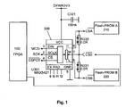
- Fig. 1 shows a schematic representation of an electronic (digital) device according to a first embodiment.
- the electronic device comprises a field programmable gate array FPGA module 100, a first memory 210 and a second memory 220 and a digital (programmable) potentiometer 300.
- a digital (programmable) potentiometer is a digitally controllable electronic component that can replicate the analog functions of a potentiometer. Non-volatile switching can be enabled with the digital potentiometer.
- the first and second memories 210, 220 may each be configured as a flash PROM.
- the digital potentiometer 300 may be configured to store at least two states.
- the first memory 210 is coupled to the FPGA 100 device, and in the second state of the digital potentiometer 300, the second memory 220 is coupled to the FPGA device 100.
- the first and second memories 210, 220 may each be used to store the data needed for booting the FPGA 100.
- the chip select signals of the FPGA can be redirected to the first or second memory 210, 220.
- the digital potentiometer 300 preferably has a Serial Peripheral Interface SPI interface.
- the FPGA 100 device may receive configuration data or update data via an interface (not shown) and store it in the first and / or second memory 210, 220.
- This data may include data required for booting the FPGA 100, for example.
- the FPGA 100 block can be booted from one of the two memories 210, 220.
- the chip select signal CS / is at least temporarily redirected.
- a successful boot-up process has been detected (eg, by reading the data needed for the boot-up process from the first or second memory 210, 220)
- a permanent translation of the digital potentiometer 310 may be performed, as shown in FIG the first or second memory is permanently coupled to the FPGA 100.
- the transmitted configuration or update data can thus be tested. If the boot was successful, then the configuration or update data was transferred without errors and stored in one of the two memories 210, 220.
- the FPGA 100 device described in the first embodiment, the first and second memories 210, 220, and the digital potentiometer 300 may be implemented in a digital microphone, for example.
- the microphone may include a software update mode that allows the software for the digital microphone to be updated.
- the solution should have a low space consumption on the printed circuit board, a low power consumption and a reliable solution.
- the solution should work without an additional controller. According to the invention, it is possible to boot two different memories 210, 220. If the data stored in one of the memories is faulty and booting is no longer possible, then the digital potentiometer 300 can switch to the other memory.
Landscapes
- Engineering & Computer Science (AREA)
- Theoretical Computer Science (AREA)
- Quality & Reliability (AREA)
- Physics & Mathematics (AREA)
- General Engineering & Computer Science (AREA)
- General Physics & Mathematics (AREA)
- Logic Circuits (AREA)
- Stored Programmes (AREA)
- Programmable Controllers (AREA)
- Input From Keyboards Or The Like (AREA)
- Design And Manufacture Of Integrated Circuits (AREA)
Description
- Die vorliegende Erfindung betrifft eine elektronische digitale Vorrichtung, welche einen FPGA (Field Programmable Gate Array) aufweist.
- Ein FPGA (Field Programmable Gate Array; vor Ort modifizierbarer Logikbaustein) stellt einen programmierbaren integrierten Schaltkreis dar. In einem FPGA können durch spezifische Konfigurationen interner Strukturen verschiedene Schaltungen gebildet werden. Der FPGA weist programmierbare logische Komponenten auf.
- Wenn ein Software-Update eines FPGA-basierten Systems durchgeführt wird, kann es vorkommen, dass die aktualisierte Software einen Fehler aufweist, so dass ein Booten bzw. Hochfahren des FPGA-basierten Systems nicht mehr möglich ist. In derartigen Fällen kann es erforderlich sein, zumindest einen Teil der Elektronikbausteine auszuwechseln. Um dies zu vermeiden, kann ein Controller in dem FPGA-basierten System vorgesehen werden, welcher dazu dienen kann, das Software-Update zu steuern.
- Als allgemeiner Stand der Technik sei auf die
US 6,079,016 und dieEP 0 939 367 A2 verwiesen. - Es ist eine Aufgabe der vorliegenden Erfindung, eine elektronische Vorrichtung mit einem FPGA vorzusehen, welcher ein Softwareupdate ermöglicht und kostengünstiger herzustellen ist.
- Diese Aufgabe wird durch eine elektronische Vorrichtung gemäß Anspruch 1 gelöst.
- Somit wird eine elektronische Vorrichtung mit einer FPGA Einheit, einem ersten und zweiten Speicher zum Speichern von Boot-Daten für die FPGA Einheit und einem digitalen Potentiometer zum Speichern einer erster und zweiten Einstellung vorgesehen. In der ersten Einstellung des Potentiometers ist der erste Speicher (zum Booten) mit der FPGA Einheit gekoppelt und in der zweiten Einstellung des Potentiometers ist der zweite Speicher zum Booten mit der FPGA Einheit gekoppelt.
- Gemäß einem Aspekt der vorliegenden Erfindung weisen die FPGA Einheit und das digitale Potentiometer jeweils eine integrierte serielle Schnittstelle auf.
- Gemäß einem weiteren Aspekt der vorliegenden Erfindung ist das digitale Potentiometer dazu geeignet, in einer Testbetriebsart die zum Booten der FPGA Einheit benötigten Signale an den zweiten Speicher weiter zu leiten, so dass die FPGA Einheit aus dem zweiten Speicher gebootet werden kann.
- Die vorliegende Erfindung betrifft ebenfalls ein digitales Mikrofon mit einer oben beschriebenen elektronischen Vorrichtung.
- Die Erfindung betrifft ebenfalls ein Verfahren zum Steuern einer elektronischen Vorrichtung mit einer FPGA (Field Programmable Gate Array) Einheit, einem ersten und zweiten Speicher und einem digitalen Potentiometer. Der erste und zweite Speicher wird zum Speichern von Boot-Daten der FPGA Einheit verwendet. Das digitale Potentiometer wird zum Speichern einer ersten und zweiten Einstellung verwendet. In der ersten Einstellung des digitalen Potentiometers wird der erste Speicher mit der FPGA Einheit gekoppelt und in der zweiten Einstellung des digitalen Potentiometers wird der zweite Speicher zum Booten mit der FPGA Einheit gekoppelt.
- Die Erfindung betrifft den Gedanken, ein Update der Betriebssoftware in zwei verschiedenen Bootsektoren der elektronischen digitalen Vorrichtung zu ermöglichen, so dass die Vorrichtung aus zwei verschiedenen Speichern booten kann. Dazu kann ein FPGA vorgesehen werden, welcher ein selbsttätiges Booten beispielsweise aus einem seriellen Flashspeicher ermöglicht. Ferner werden zumindest zwei verschiedene Bootsektoren in dem oder den Speicher(n) vorgesehen. Üblicherweise erzeugt das FPGA SPI-Bus Signale wie beispielsweise CS\, MOSI, MISO, SCLK zum Auslesen der seriellen Flash PROM. Indem die Chip-Select Signale CS umgeleitet werden, können verschiedene Boot PROMs angesprochen werden.
- Das Umleiten der Chip-Select Signale kann beispielsweise mittels eines programmierbaren (digitalen) Potentiometers erfolgen. Die Schleiferposition des programmierbaren Potentiometers kann sowohl temporär bzw. volatile als auch permanent bzw. non-volatile gesetzt werden. Das digitale programmierbare Potentiometer weist vorzugsweise eine SPI-Schnittstelle auf. Weitere Ausgestaltungen der Erfindung sind Gegenstand der Unteransprüche.
- Gemäß der Erfindung wird das elektronische Potentiometer als Umschalter (zwischen zwei Speichern) für eine Booteinstellung eines FGPA verwendet. Durch die permanente Speicherung der Schleiferposition im Potentiometer kann der stromlose Zustand überbrückt werden.
- Vorteile und Ausführungsbeispiele der Erfindung werden nachstehend unter Bezugnahme auf die Zeichnung näher erläutert.
- Fig. 1
- zeigt eine schematische Darstellung einer elektronischen Digitalvorrichtung gemäß einem ersten Ausführungsbeispiel
-
Fig. 1 zeigt eine schematische Darstellung einer elektronischen (Digital) Vorrichtung gemäß einem ersten Ausführungsbeispiel. Die elektronische Vorrichtung weist einen Field Programmable Gate Array FPGA Baustein 100, einen ersten Speicher 210 und einen zweiten Speicher 220 sowie ein digitales (programmierbares) Potentiometer 300 auf. Ein digitales (programmierbares) Potentiometer stellt eine digital steuerbare elektronische Komponente dar, welche die analogen Funktionen eines Potentiometers nachbilden kann. Mit dem digitalen Potentiometer kann ein nicht flüchtiges Umschalten ermöglicht werden. Der erste und zweite Speicher 210, 220 kann jeweils als ein Flash PROM ausgestaltet sein. Das digitale Potentiometer 300 kann dazu ausgestaltet sein, zumindest zwei Zustände zu speichern. In dem ersten Zustand des Potentiometers 300 wird der erste Speicher 210 mit dem FPGA 100 Baustein gekoppelt und in dem zweiten Zustand des digitalen Potentiometers 300 wird der zweite Speicher 220 mit dem FPGA Baustein 100 gekoppelt. Der erste und zweite Speicher 210, 220 kann jeweils zum Speichern der für den Boot-Vorgang des FPGA 100 benötigten Daten verwendet werden. Mittels des digitalen Potentiometers 300 können beispielsweise die Chip-Select Signale des FPGA zu dem ersten oder zweiten Speicher 210, 220 umgeleitet werden. Das digitale Potentiometer 300 weist vorzugsweise eine Serial Peripheral Interface SPI-Schnittstelle auf. - Der FPGA 100 Baustein kann über eine (nicht gezeigte) Schnittstelle Konfigurationsdaten oder Aktualisierungsdaten empfangen und in dem ersten und/oder zweiten Speicher 210, 220 speichern. Diese Daten können Daten enthalten, welche beispielsweise zum Booten des FPGA 100 benötigt werden. Nachdem die Daten in dem ersten und/oder zweiten Speicher 210, 220 gespeichert sind, kann der FPGA 100 Baustein aus einem der beiden Speicher 210, 220 gebootet werden. In einer Test-Boot-Betriebsart wird das Chip-Select Signal CS/ zumindest temporär umgeleitet. Nachdem ein erfolgreicher Boot-up Vorgang (z. B. indem die für den Boot-up Vorgang benötigten Daten aus dem ersten oder zweiten Speicher 210, 220 gelesen worden sind) erfasst worden ist, kann ein permanentes Umsetzen des digitalen Potentiometers 310 erfolgen, so dass der erste oder zweite Speicher permanent mit dem FPGA 100 gekoppelt ist. Insbesondere können somit die übertragenen Konfigurations- bzw. Aktualisierungsdaten getestet werden. Falls der Bootvorgang erfolgreich war, dann wurden die Konfigurations- bzw. Aktualisierungsdaten fehlerfrei übertragen und in einem der beiden Speicher 210, 220 gespeichert.
- Der gemäß dem ersten Ausführungsbeispiel beschriebene FPGA 100 Baustein, der erste und zweite Speicher 210, 220 und das digitale Potentiometer 300 können beispielsweise in einem digitalen Mikrofon implementiert werden.
- Das Mikrofon kann eine Betriebsart Softwareupdate aufweisen, welches es ermöglicht, die Software für das digitale Mikrofon zu aktualisieren. Dazu sollte die Lösung einen geringen Platzverbrauch auf der Leiterplatine, einen geringen Energieverbrauch und eine betriebssichere Lösung aufweisen. Vorzugsweise sollte die Lösung ohne einen zusätzlichen Controller auskommen. Gemäß der Erfindung ist es möglich, zwei verschiedene Speicher 210, 220 zu booten. Wenn die in einem der Speicher gespeicherten Daten fehlerhaft sind und ein Booten nicht mehr möglich ist, dann kann durch das digitale Potentiometer 300 zu dem anderen Speicher umgeschaltet werden.
Claims (5)
- Elektronische Vorrichtung, mit
einer FPGA Einheit (100),
einem ersten und zweiten Speicher (210, 220) zum Speichern von Bootdaten für die FPGA Einheit (100), und
einem digitalen Potentiometer (300) zum Speichern einer ersten und zweiten Einstellung,
wobei in der ersten Einstellung des digitalen Potentiometers (300) der erste Speicher (210) mit der FPGA Einheit (100) gekoppelt ist und wobei in der zweiten Einstellung des digitalen Potentiometers (300) der zweite Speicher (220) mit der FPGA Einheit (100) gekoppelt ist. - Vorrichtung nach Anspruch 1, wobei
die FPGA Einheit (100) und das digitale Potentiometer (300) jeweils über eine integrierte serielle Schnittstelle (SPI) verfügen. - Vorrichtung nach Anspruch 1 oder 2, wobei das digitale Potentiometer (300) dazu geeignet ist, in einer Testbetriebsart die zum Booten der FPGA Einheit (100) benötigten Signale an den zweiten Speicher (220) weiterzuleiten, so dass die FPGA Einheit aus dem zweiten Speicher (220) gebootet wird.
- Digitales Mikrofon mit einer elektronischen Vorrichtung nach einem der Ansprüche 1 bis 3.
- Verfahren zum Steuern einer elektronischen Vorrichtung, welche eine FPGA Einheit (100) aufweist, mit den Schritten:Speichern von Boot-Daten für die FPGA Einheit in einem ersten und/oder zweiten Speicher (210, 220),Speichern einer ersten und zweiten Einstellung in einem digitalen Potentiometer (300),Koppeln des ersten Speichers (210) mit der FPGA Einheit (100) in der ersten Einstellung des digitalen Potentiometers (300) undKoppeln des zweiten Speichers (220) mit der FPGA Einheit (100) zum Booten der FPGA Einheit (100) in der zweiten Einstellung des digitalen Potentiometers (300).
Applications Claiming Priority (2)
| Application Number | Priority Date | Filing Date | Title |
|---|---|---|---|
| DE102007060234A DE102007060234A1 (de) | 2007-12-14 | 2007-12-14 | Elektronische digitale Vorrichtung |
| PCT/EP2008/010646 WO2009077149A1 (de) | 2007-12-14 | 2008-12-15 | Elektronische digitale vorrichtung |
Publications (2)
| Publication Number | Publication Date |
|---|---|
| EP2229626A1 EP2229626A1 (de) | 2010-09-22 |
| EP2229626B1 true EP2229626B1 (de) | 2011-10-19 |
Family
ID=40561763
Family Applications (1)
| Application Number | Title | Priority Date | Filing Date |
|---|---|---|---|
| EP08861872A Active EP2229626B1 (de) | 2007-12-14 | 2008-12-15 | Elektronische digitale vorrichtung |
Country Status (5)
| Country | Link |
|---|---|
| US (1) | US8572363B2 (de) |
| EP (1) | EP2229626B1 (de) |
| AT (1) | ATE529806T1 (de) |
| DE (1) | DE102007060234A1 (de) |
| WO (1) | WO2009077149A1 (de) |
Family Cites Families (11)
| Publication number | Priority date | Publication date | Assignee | Title |
|---|---|---|---|---|
| JP2772103B2 (ja) * | 1990-03-28 | 1998-07-02 | 株式会社東芝 | 計算機システム立上げ方式 |
| KR100198382B1 (ko) * | 1996-05-07 | 1999-06-15 | 윤종용 | 멀티-부팅 기능을 갖는 컴퓨터 장치 |
| US5987605A (en) * | 1998-02-28 | 1999-11-16 | Hewlett-Packard Co. | Methods and apparatus for dual-boot memory selection, update, and recovery in a programmable device |
| US6219721B1 (en) * | 1998-10-26 | 2001-04-17 | Chen-Chang Su | Computer in which multiple operating systems are installed in different peripheral access devices |
| US6754818B1 (en) * | 2000-08-31 | 2004-06-22 | Sun Microsystems, Inc. | Method and system for bootstrapping from a different boot image when computer system is turned on or reset |
| US7146598B2 (en) * | 2002-11-07 | 2006-12-05 | Computer Network Technoloy Corp. | Method and apparatus for configuring a programmable logic device |
| US7146541B2 (en) * | 2003-05-20 | 2006-12-05 | Lucent Technologies Inc. | Back out provision for failed programmable hardware update |
| JP4207881B2 (ja) * | 2004-11-15 | 2009-01-14 | ソニー株式会社 | マイクシステムおよびマイク装置 |
| JP2007148604A (ja) * | 2005-11-25 | 2007-06-14 | Elpida Memory Inc | 可変電圧電源装置 |
| US7487344B2 (en) * | 2006-03-03 | 2009-02-03 | Alcatel Lucent | Implementing a microprocessor boot configuration prom within an FPGA |
| US7822958B1 (en) * | 2006-03-10 | 2010-10-26 | Altera Corporation | Booting mechanism for FPGA-based embedded system |
-
2007
- 2007-12-14 DE DE102007060234A patent/DE102007060234A1/de not_active Withdrawn
-
2008
- 2008-12-15 US US12/747,153 patent/US8572363B2/en not_active Expired - Fee Related
- 2008-12-15 EP EP08861872A patent/EP2229626B1/de active Active
- 2008-12-15 AT AT08861872T patent/ATE529806T1/de active
- 2008-12-15 WO PCT/EP2008/010646 patent/WO2009077149A1/de not_active Ceased
Also Published As
| Publication number | Publication date |
|---|---|
| EP2229626A1 (de) | 2010-09-22 |
| ATE529806T1 (de) | 2011-11-15 |
| US8572363B2 (en) | 2013-10-29 |
| US20100325407A1 (en) | 2010-12-23 |
| DE102007060234A1 (de) | 2009-06-18 |
| WO2009077149A1 (de) | 2009-06-25 |
Similar Documents
| Publication | Publication Date | Title |
|---|---|---|
| EP2318920B1 (de) | Steuergerät für ein fahrzeug und verfahren für eine datenaktualisierung für ein steuergerät für ein fahrzeug | |
| EP2943748B1 (de) | Verfahren und vorrichtung zum verwalten von kartendaten einer digitalen karte einer navigationseinrichtung | |
| DE102015217933B4 (de) | Vorrichtung zum Verarbeiten von Daten und Verfahren zum Betreiben einer solchen Vorrichtung | |
| DE102017211433A1 (de) | Verfahren zum Durchführen eines Funktionstests eines Steuergeräts in einem Hardware-in-the-Loop-Test, HIL-Test, sowie HIL-Prüfstand und Steuergerät | |
| DE10231956A1 (de) | Verfahren und Vorrichtung zur systeminternen Programmierung durch einen gemeinsamen Verbindungspunkt von programmierbaren logischen Bauelementen auf mehreren Schaltungsplatinen eines Systems | |
| DE102004012279B3 (de) | Verfahren und Vorrichtung zum Speicherselbsttest von eingebetteten Speichern in Halbleiterchips | |
| DE102007045851A1 (de) | Elektronische Vorrichtung, Verfahren zum Betreiben einer elektronischen Vorrichtung, Speicherschaltung und Verfahren zum Betreiben einer Speicherschaltung | |
| DE10322748B4 (de) | Elektronische Steuereinrichtung | |
| DE60309157T2 (de) | Speichersystem mit Fehlererkennungsvorrichtung | |
| DE102009005399A1 (de) | Verfahren und Kommunikationssystem zum Konfigurieren eines einen Logikbaustein enthaltenden Kommunikationsmoduls | |
| DE3820728A1 (de) | Verfahren zum pruefen eines festwertspeichers und anordnung zur durchfuehrung des verfahrens | |
| EP2229626A1 (de) | Elektronische digitale vorrichtung | |
| DE102009002898A1 (de) | Verfahren zur Aktualisierung eines Steuergeräts eines Fahrzeugs | |
| EP3399425B1 (de) | Verfahren zur erkennung einer verdrahtungstopologie | |
| DE10303654A1 (de) | Integrierte Halbleiterschaltung mit eingebauter Selbsttestfunktion und zugehöriges System | |
| EP0214451A2 (de) | Anordnung zum Programmieren eines Festwertspeichers | |
| DE19748181B4 (de) | Verfahren zum Prüfen einer Funktion oder Einrichtung eines Fahrzeugs | |
| DE102018221786B4 (de) | Anordnung mit einem ersten Steuergerät für ein Fahrzeug und einem zweiten Steuergerät für ein Fahrzeug; wobei das erste Steuergerät und das zweite Steuergerät jeweils Getriebesteuergeräte sind und in Abhängigkeit von in einer Software enthaltenen Anweisungen ein Getriebe des Fahrzeugs steuern oder regeln | |
| WO2009103728A1 (de) | Verfahren und vorrichtung zum speichern von informationsdaten | |
| DE102018214980A1 (de) | Rechnersystem und Betriebsverfahren dafür mit verbesserter Zuverlässigkeit | |
| EP1745386B1 (de) | Steuerungsschaltung für eine busplatine eines computersystems | |
| DE102005017298B4 (de) | Verfahren und Vorrichtung zum Schreiben eines Ablaufsprogramms in eine Speichervorrichtung einer programmgesteuerten Steuervorrichtung | |
| DE19733113B4 (de) | Verfahren zum Testen einer elektronischen Baugruppe und elektronische Baugruppe mit Testhilfe | |
| DE102023110712A1 (de) | System zum testen eines elektronischen geräts | |
| DE69803851T2 (de) | Verfahren zur steuerung eines integrierten mikroprozessors mit einem festwertprogrammspeicher und intergrierte schaltung zur durchführung dieses verfahrens |
Legal Events
| Date | Code | Title | Description |
|---|---|---|---|
| PUAI | Public reference made under article 153(3) epc to a published international application that has entered the european phase |
Free format text: ORIGINAL CODE: 0009012 |
|
| 17P | Request for examination filed |
Effective date: 20100714 |
|
| AK | Designated contracting states |
Kind code of ref document: A1 Designated state(s): AT BE BG CH CY CZ DE DK EE ES FI FR GB GR HR HU IE IS IT LI LT LU LV MC MT NL NO PL PT RO SE SI SK TR |
|
| AX | Request for extension of the european patent |
Extension state: AL BA MK RS |
|
| RIN1 | Information on inventor provided before grant (corrected) |
Inventor name: FREY, TOM-FABIAN Inventor name: WATERMANN, JAN |
|
| DAX | Request for extension of the european patent (deleted) | ||
| GRAP | Despatch of communication of intention to grant a patent |
Free format text: ORIGINAL CODE: EPIDOSNIGR1 |
|
| GRAS | Grant fee paid |
Free format text: ORIGINAL CODE: EPIDOSNIGR3 |
|
| GRAA | (expected) grant |
Free format text: ORIGINAL CODE: 0009210 |
|
| AK | Designated contracting states |
Kind code of ref document: B1 Designated state(s): AT BE BG CH CY CZ DE DK EE ES FI FR GB GR HR HU IE IS IT LI LT LU LV MC MT NL NO PL PT RO SE SI SK TR |
|
| REG | Reference to a national code |
Ref country code: GB Ref legal event code: FG4D Free format text: NOT ENGLISH |
|
| REG | Reference to a national code |
Ref country code: CH Ref legal event code: EP |
|
| REG | Reference to a national code |
Ref country code: IE Ref legal event code: FG4D |
|
| REG | Reference to a national code |
Ref country code: DE Ref legal event code: R096 Ref document number: 502008005293 Country of ref document: DE Effective date: 20111229 |
|
| REG | Reference to a national code |
Ref country code: NL Ref legal event code: VDEP Effective date: 20111019 |
|
| LTIE | Lt: invalidation of european patent or patent extension |
Effective date: 20111019 |
|
| PG25 | Lapsed in a contracting state [announced via postgrant information from national office to epo] |
Ref country code: IS Free format text: LAPSE BECAUSE OF FAILURE TO SUBMIT A TRANSLATION OF THE DESCRIPTION OR TO PAY THE FEE WITHIN THE PRESCRIBED TIME-LIMIT Effective date: 20120219 Ref country code: NO Free format text: LAPSE BECAUSE OF FAILURE TO SUBMIT A TRANSLATION OF THE DESCRIPTION OR TO PAY THE FEE WITHIN THE PRESCRIBED TIME-LIMIT Effective date: 20120119 Ref country code: LT Free format text: LAPSE BECAUSE OF FAILURE TO SUBMIT A TRANSLATION OF THE DESCRIPTION OR TO PAY THE FEE WITHIN THE PRESCRIBED TIME-LIMIT Effective date: 20111019 |
|
| REG | Reference to a national code |
Ref country code: IE Ref legal event code: FD4D |
|
| PG25 | Lapsed in a contracting state [announced via postgrant information from national office to epo] |
Ref country code: HR Free format text: LAPSE BECAUSE OF FAILURE TO SUBMIT A TRANSLATION OF THE DESCRIPTION OR TO PAY THE FEE WITHIN THE PRESCRIBED TIME-LIMIT Effective date: 20111019 Ref country code: GR Free format text: LAPSE BECAUSE OF FAILURE TO SUBMIT A TRANSLATION OF THE DESCRIPTION OR TO PAY THE FEE WITHIN THE PRESCRIBED TIME-LIMIT Effective date: 20120120 Ref country code: SE Free format text: LAPSE BECAUSE OF FAILURE TO SUBMIT A TRANSLATION OF THE DESCRIPTION OR TO PAY THE FEE WITHIN THE PRESCRIBED TIME-LIMIT Effective date: 20111019 Ref country code: SI Free format text: LAPSE BECAUSE OF FAILURE TO SUBMIT A TRANSLATION OF THE DESCRIPTION OR TO PAY THE FEE WITHIN THE PRESCRIBED TIME-LIMIT Effective date: 20111019 Ref country code: LV Free format text: LAPSE BECAUSE OF FAILURE TO SUBMIT A TRANSLATION OF THE DESCRIPTION OR TO PAY THE FEE WITHIN THE PRESCRIBED TIME-LIMIT Effective date: 20111019 Ref country code: PT Free format text: LAPSE BECAUSE OF FAILURE TO SUBMIT A TRANSLATION OF THE DESCRIPTION OR TO PAY THE FEE WITHIN THE PRESCRIBED TIME-LIMIT Effective date: 20120220 Ref country code: NL Free format text: LAPSE BECAUSE OF FAILURE TO SUBMIT A TRANSLATION OF THE DESCRIPTION OR TO PAY THE FEE WITHIN THE PRESCRIBED TIME-LIMIT Effective date: 20111019 |
|
| PG25 | Lapsed in a contracting state [announced via postgrant information from national office to epo] |
Ref country code: CY Free format text: LAPSE BECAUSE OF FAILURE TO SUBMIT A TRANSLATION OF THE DESCRIPTION OR TO PAY THE FEE WITHIN THE PRESCRIBED TIME-LIMIT Effective date: 20111019 |
|
| BERE | Be: lapsed |
Owner name: SENNHEISER ELECTRONIC G.M.B.H. & CO. KG Effective date: 20111231 |
|
| PG25 | Lapsed in a contracting state [announced via postgrant information from national office to epo] |
Ref country code: EE Free format text: LAPSE BECAUSE OF FAILURE TO SUBMIT A TRANSLATION OF THE DESCRIPTION OR TO PAY THE FEE WITHIN THE PRESCRIBED TIME-LIMIT Effective date: 20111019 Ref country code: MC Free format text: LAPSE BECAUSE OF NON-PAYMENT OF DUE FEES Effective date: 20111231 Ref country code: SK Free format text: LAPSE BECAUSE OF FAILURE TO SUBMIT A TRANSLATION OF THE DESCRIPTION OR TO PAY THE FEE WITHIN THE PRESCRIBED TIME-LIMIT Effective date: 20111019 Ref country code: DK Free format text: LAPSE BECAUSE OF FAILURE TO SUBMIT A TRANSLATION OF THE DESCRIPTION OR TO PAY THE FEE WITHIN THE PRESCRIBED TIME-LIMIT Effective date: 20111019 Ref country code: IE Free format text: LAPSE BECAUSE OF FAILURE TO SUBMIT A TRANSLATION OF THE DESCRIPTION OR TO PAY THE FEE WITHIN THE PRESCRIBED TIME-LIMIT Effective date: 20111019 Ref country code: CZ Free format text: LAPSE BECAUSE OF FAILURE TO SUBMIT A TRANSLATION OF THE DESCRIPTION OR TO PAY THE FEE WITHIN THE PRESCRIBED TIME-LIMIT Effective date: 20111019 Ref country code: BG Free format text: LAPSE BECAUSE OF FAILURE TO SUBMIT A TRANSLATION OF THE DESCRIPTION OR TO PAY THE FEE WITHIN THE PRESCRIBED TIME-LIMIT Effective date: 20120119 |
|
| PLBE | No opposition filed within time limit |
Free format text: ORIGINAL CODE: 0009261 |
|
| STAA | Information on the status of an ep patent application or granted ep patent |
Free format text: STATUS: NO OPPOSITION FILED WITHIN TIME LIMIT |
|
| PG25 | Lapsed in a contracting state [announced via postgrant information from national office to epo] |
Ref country code: IT Free format text: LAPSE BECAUSE OF FAILURE TO SUBMIT A TRANSLATION OF THE DESCRIPTION OR TO PAY THE FEE WITHIN THE PRESCRIBED TIME-LIMIT Effective date: 20111019 Ref country code: PL Free format text: LAPSE BECAUSE OF FAILURE TO SUBMIT A TRANSLATION OF THE DESCRIPTION OR TO PAY THE FEE WITHIN THE PRESCRIBED TIME-LIMIT Effective date: 20111019 Ref country code: RO Free format text: LAPSE BECAUSE OF FAILURE TO SUBMIT A TRANSLATION OF THE DESCRIPTION OR TO PAY THE FEE WITHIN THE PRESCRIBED TIME-LIMIT Effective date: 20111019 |
|
| 26N | No opposition filed |
Effective date: 20120720 |
|
| PG25 | Lapsed in a contracting state [announced via postgrant information from national office to epo] |
Ref country code: BE Free format text: LAPSE BECAUSE OF NON-PAYMENT OF DUE FEES Effective date: 20111231 |
|
| REG | Reference to a national code |
Ref country code: DE Ref legal event code: R097 Ref document number: 502008005293 Country of ref document: DE Effective date: 20120720 |
|
| PG25 | Lapsed in a contracting state [announced via postgrant information from national office to epo] |
Ref country code: MT Free format text: LAPSE BECAUSE OF FAILURE TO SUBMIT A TRANSLATION OF THE DESCRIPTION OR TO PAY THE FEE WITHIN THE PRESCRIBED TIME-LIMIT Effective date: 20111019 |
|
| PG25 | Lapsed in a contracting state [announced via postgrant information from national office to epo] |
Ref country code: ES Free format text: LAPSE BECAUSE OF FAILURE TO SUBMIT A TRANSLATION OF THE DESCRIPTION OR TO PAY THE FEE WITHIN THE PRESCRIBED TIME-LIMIT Effective date: 20120130 |
|
| PG25 | Lapsed in a contracting state [announced via postgrant information from national office to epo] |
Ref country code: LU Free format text: LAPSE BECAUSE OF NON-PAYMENT OF DUE FEES Effective date: 20111215 |
|
| PG25 | Lapsed in a contracting state [announced via postgrant information from national office to epo] |
Ref country code: FI Free format text: LAPSE BECAUSE OF FAILURE TO SUBMIT A TRANSLATION OF THE DESCRIPTION OR TO PAY THE FEE WITHIN THE PRESCRIBED TIME-LIMIT Effective date: 20111019 |
|
| REG | Reference to a national code |
Ref country code: CH Ref legal event code: PL |
|
| PG25 | Lapsed in a contracting state [announced via postgrant information from national office to epo] |
Ref country code: TR Free format text: LAPSE BECAUSE OF FAILURE TO SUBMIT A TRANSLATION OF THE DESCRIPTION OR TO PAY THE FEE WITHIN THE PRESCRIBED TIME-LIMIT Effective date: 20111019 |
|
| PG25 | Lapsed in a contracting state [announced via postgrant information from national office to epo] |
Ref country code: CH Free format text: LAPSE BECAUSE OF NON-PAYMENT OF DUE FEES Effective date: 20121231 Ref country code: LI Free format text: LAPSE BECAUSE OF NON-PAYMENT OF DUE FEES Effective date: 20121231 Ref country code: HU Free format text: LAPSE BECAUSE OF FAILURE TO SUBMIT A TRANSLATION OF THE DESCRIPTION OR TO PAY THE FEE WITHIN THE PRESCRIBED TIME-LIMIT Effective date: 20111019 |
|
| REG | Reference to a national code |
Ref country code: AT Ref legal event code: MM01 Ref document number: 529806 Country of ref document: AT Kind code of ref document: T Effective date: 20131215 |
|
| PG25 | Lapsed in a contracting state [announced via postgrant information from national office to epo] |
Ref country code: AT Free format text: LAPSE BECAUSE OF NON-PAYMENT OF DUE FEES Effective date: 20131215 |
|
| REG | Reference to a national code |
Ref country code: FR Ref legal event code: PLFP Year of fee payment: 8 |
|
| REG | Reference to a national code |
Ref country code: FR Ref legal event code: PLFP Year of fee payment: 9 |
|
| REG | Reference to a national code |
Ref country code: FR Ref legal event code: PLFP Year of fee payment: 10 |
|
| PGFP | Annual fee paid to national office [announced via postgrant information from national office to epo] |
Ref country code: DE Payment date: 20241204 Year of fee payment: 17 |
|
| PGFP | Annual fee paid to national office [announced via postgrant information from national office to epo] |
Ref country code: GB Payment date: 20241218 Year of fee payment: 17 |
|
| PGFP | Annual fee paid to national office [announced via postgrant information from national office to epo] |
Ref country code: FR Payment date: 20241218 Year of fee payment: 17 |
|
| REG | Reference to a national code |
Ref country code: DE Ref legal event code: R081 Ref document number: 502008005293 Country of ref document: DE Owner name: SENNHEISER ELECTRONIC SE & CO. KG, DE Free format text: FORMER OWNER: SENNHEISER ELECTRONIC GMBH & CO. KG, 30900 WEDEMARK, DE |