EP2228753B1 - Bildverarbeitungsvorrichtung und Bildverarbeitungsverfahren - Google Patents
Bildverarbeitungsvorrichtung und Bildverarbeitungsverfahren Download PDFInfo
- Publication number
- EP2228753B1 EP2228753B1 EP10154035.9A EP10154035A EP2228753B1 EP 2228753 B1 EP2228753 B1 EP 2228753B1 EP 10154035 A EP10154035 A EP 10154035A EP 2228753 B1 EP2228753 B1 EP 2228753B1
- Authority
- EP
- European Patent Office
- Prior art keywords
- edge code
- image
- value
- edge
- code value
- Prior art date
- Legal status (The legal status is an assumption and is not a legal conclusion. Google has not performed a legal analysis and makes no representation as to the accuracy of the status listed.)
- Not-in-force
Links
Images








Classifications
-
- G—PHYSICS
- G06—COMPUTING OR CALCULATING; COUNTING
- G06V—IMAGE OR VIDEO RECOGNITION OR UNDERSTANDING
- G06V10/00—Arrangements for image or video recognition or understanding
- G06V10/94—Hardware or software architectures specially adapted for image or video understanding
-
- G—PHYSICS
- G06—COMPUTING OR CALCULATING; COUNTING
- G06V—IMAGE OR VIDEO RECOGNITION OR UNDERSTANDING
- G06V10/00—Arrangements for image or video recognition or understanding
- G06V10/40—Extraction of image or video features
- G06V10/46—Descriptors for shape, contour or point-related descriptors, e.g. scale invariant feature transform [SIFT] or bags of words [BoW]; Salient regional features
-
- G—PHYSICS
- G06—COMPUTING OR CALCULATING; COUNTING
- G06V—IMAGE OR VIDEO RECOGNITION OR UNDERSTANDING
- G06V10/00—Arrangements for image or video recognition or understanding
- G06V10/70—Arrangements for image or video recognition or understanding using pattern recognition or machine learning
- G06V10/74—Image or video pattern matching; Proximity measures in feature spaces
- G06V10/75—Organisation of the matching processes, e.g. simultaneous or sequential comparisons of image or video features; Coarse-fine approaches, e.g. multi-scale approaches; using context analysis; Selection of dictionaries
- G06V10/752—Contour matching
Definitions
- the present invention relates to an image processing device and an image processing method for performing pattern matching process and the like.
- pattern matching process based on a standard pattern (hereinafter also referred to as "mode! image") registered in advance is used on an input image obtained by imaging a target (hereinafter also referred to as "target work"). Defects such as scratches and dust that appear on the target work can be detected, and a portion on the target work similar to the model image can be searched through the pattern matching process.
- mode! image a standard pattern registered in advance
- target work an input image obtained by imaging a target
- Defects such as scratches and dust that appear on the target work can be detected, and a portion on the target work similar to the model image can be searched through the pattern matching process.
- a window needs to be set in the input image obtained by imaging the target work, and a partial image (image information) in the window and the model image registered in advance need to be compared.
- the image information of each pixel (typically, gray value of 8 bits) is sequentially outputted from the imaging device along a predetermined scanning direction. In other words, the image information of the pixels contained in the set window is outputted not at the same timing, but in time-series with a delay time.
- a buffer memory of a predetermined amount (typically, worth one screen) is prepared, and the image information from the imaging device is sequentially stored in the buffer memory and the pattern matching process is executed on the stored image information to resolve such a temporal shift.
- the image processing device for performing the pattern matching process thus has problems in that the circuit configuration enlarges and becomes complicating.
- edge portion
- EC Error Code
- the image processing device disclosed in International Publication No. WO93/18471 pamphlet is configured to perform the pattern matching process based on the gray value of the input image, and is not to perform the pattern matching based on the edge code.
- the circuit configuration thus enlarges and becomes complicating when performing the pattern matching based on the edge code.
- the processing time also becomes long compared to the hardware when implemented with the software process using a processor.
- JACOBUS C ET AL "Intermediate-Level Vision-Building Vertex-String-Surface (V-S-S) Graphs", COMPUTER GRAPHICS AND IMAGE PROCESSING, US, vol. 15, no. 4, 1 April 1981 (1981-04-01), pages 339-363, XP 001375239, ISSN: 0146-664X , BARUCH O ET AL: "SEGMENTATION OF TWO-DIMENSIONAL BOUNDARIES USING THE CHAIN CODE", PATTERN-RECOGNITION, ELSEVIER, GB, vol. 21, no.
- the present invention has been devised to solve the problems described above, and an object thereof is to provide an image processing device and an image processing method capable of implementing pattern matching based on an edge code at relatively high speed with a smaller circuit configuration.
- an image processing device includes a generation unit for generating an edge code image based on a gray value of an input image.
- Each element contained in the edge code image includes an edge code value and information indicating valid/invalid of the edge code value.
- the image processing device further includes a compression unit for compressing the edge code image by assigning information representing the edge code value for an element having a valid edge code value to an element having an invalid edge code value, a storage unit for sequentially storing the compressed edge code image; a decompression unit for decompressing the compressed edge code image stored in the storage unit; and a comparator for calculating a similarity degree between the edge code image decompressed by the decompression unit and a model image defined in advance.
- the generation unit is preferably inputted with the gray value of each pixel contained in the input image in a predetermined order; the generation unit sequentially generates the edge code value for every input of the gray value; and the compression unit outputs information for specifying the valid edge code value in correspondence to an element, which is generated before an element having a valid edge code value and which has an invalid edge code value.
- the compression unit When a first zone in which the valid edge code value continues, a second zone, following the first zone, in which the invalid edge code value continues, and a third zone, following the second zone, in which the valid edge code value continues appear in a profile of the sequentially outputted edge code value, the compression unit preferably outputs increase/decrease information from the edge code value contained in the first zone to the edge code value contained in the third zone in correspondence with an element corresponding to the second zone.
- the compression unit preferably includes a plurality of first delay elements, connected in series, sequentially inputted with the edge code values generated by the generation unit at a predetermined cycle, a plurality of second delay elements, connected in series, sequentially inputted with the information indicating valid/invalid of the edge code value generated by the generation unit at the predetermined cycle, a position specifying unit for specifying a position of the second delay element storing information indicating valid of the information indicating valid/invalid of the edge code value held in the plurality of second delay elements, an extracting unit for extracting the edge code value held in the first delay element corresponding to the position specified by the position specifying unit of the edge code values held in the plurality of first delay elements, and a difference calculation unit for sequentially outputting a difference between the edge code value extracted by the extracting unit in a previous cycle and the edge code value extracted by the extracting unit in a current cycle as the increase/decrease information.
- the decompression unit includes an integrating portion for integrating the sequentially outputted increase/decrease information.
- the decompression unit includes a plurality of third delay elements, connected in series, sequentially inputted with the edge code value held at a predetermined position of the storage unit at the predetermined cycle, and a selection unit for outputting, to the integrating portion, the edge code value held in the delay element corresponding to relative positional information contained in the model image of the plurality of third delay elements.
- the model image includes an edge code value at an evaluation position for calculating the similarity degree, and the relative positional information indicating a difference in a relative position between the evaluation position and another evaluation position.
- the generation unit preferably includes a detector for detecting an edge intensity at each pixel of the input image, and a determination unit for outputting information indicating that the corresponding edge code value is valid when the edge intensity detected by the detector exceeds a predetermined value.
- an image processing method includes the steps of generating an edge code image based on a gray value of an input image. Each element contained in the edge code image including an edge code value and information indicating valid/invalid of the edge code value.
- the image processing method further includes the steps of compressing the edge code image by assigning information representing the edge code value for an element having a valid edge code value to an element having an invalid edge code value; sequentially storing the compressed edge code image; decompressing the stored compressed edge code image; and calculating a similarity degree between the decompressed edge code image and a model image defined in advance.
- the pattern matching based on the edge code can be executed with a smaller circuit configuration and at a relatively high speed.
- Fig. 1 is a schematic view showing an overall configuration of a pattern matching processing system 1 according to a first embodiment of the present invention.
- the pattern matching processing system 1 includes an image processing device 100 and an imaging device 200.
- the pattern matching processing system 1 is representatively incorporated in a production line and the like, and executes pattern matching process based on a model image registered in advance ("edge code image" is used as hereinafter described) with respect to a target work 2.
- the target work 2 is conveyed by a conveying mechanism 6 such as a belt conveyor, and the conveyed target work 2 is imaged by the imaging device 200 at a predetermined timing.
- An image (hereinafter also referred to as "input image") obtained through imaging by the imaging device 200 is outputted to the image processing device 100.
- the image processing device 100 executes the pattern matching process on the input image received from the imaging device 200, and displays the result on a mounted display unit or outputs a result to an external device.
- Figs. 2A and 2B are views describing an outline of the pattern matching process based on an edge code according to the embodiment of the present invention.
- Fig. 2A shows one example of the input image
- Fig. 2B shows one example in which an edge code image obtained from the input image shown in Fig. 2A is visualized.
- a region showing an alphabet "A" exists on a substantially even background.
- a portion corresponding to a contour of the alphabet "A" (white region in Fig. 2B ) as shown in Fig. 2B is extracted as a portion of high edge intensity.
- a value indicating a changing direction of the extracted edge is calculated as an edge code value (EC value) at the relevant edge position.
- EC value edge code value
- a direction in which the edge exists i.e., direction (angle) of arrow shown in Fig. 2B
- the edge code is calculated as one example of the value indicating the changing direction of the edge.
- Fig. 3 is a view describing a calculation procedure of the edge code according to the present embodiment.
- a case in which scanning is performed in a B direction to perform the edge extraction process on the image as shown in Fig. 3 will be considered.
- the edge extraction process an edge intensity is detected based on a gray value of the relevant pixel and a gray value of the surrounding pixels, and a maximum value in the profile of the edge intensity with respect to the B direction is extracted as the edge for each pixel existing in the B direction.
- a coordinate E(x, y) is extracted as one part of an edge EDG. In which direction the edge EDG continues is then determined based on the gray value of the surrounding pixel of the extracted coordinate E(x, y), and the like. In other words, a tangent line vector C at the coordinate E(x, y) of the edge EDG is calculated.
- An angle Ec(x, y) formed by the tangent vector C and a reference vector (B direction in the example shown in Fig. 3 ) is calculated as an edge code.
- the angle Ec(x, y) may be defined with 0° to 360° as an effective range, or may be defined with 0° to 180° as an effective range. In the latter case, it becomes a relative angular difference of the tangent line vector C and the reference vector.
- a changing direction of a shading in the extracted edge may be calculated as an edge code.
- a direction orthogonal to the tangent line vector C shown in Fig. 3 becomes the edge code.
- each element configuring the edge code image includes an edge code value corresponded to each coordinate of the input image.
- each element configuring the edge code image further includes information indicating valid/invalid of the valid edge code value (typically, "valid/invalid flag” described later).
- valid/invalid flag typically, "valid/invalid flag” described later.
- the edge code image is created and registered in advance for the model image used in the pattern matching process.
- the edge code image for the registered model and the edge code image generated from the input image are compared to calculate a similarity degree thereof.
- a portion most similar to the model image is searched based on the calculated similarity degree.
- the model image for a partial image smaller than the entire size of the input image is used in the pattern matching process.
- a window having a size corresponding to the model image registered in advance is sequentially set on the input image, the position of the partial image having the highest degree of similarly with the model image of the partial images in each sequentially set window is searched, and the position obtained by such a search is outputted as a result.
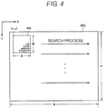
- Fig. 4 is a view describing an outline of the pattern matching process (search process) according to the embodiment of the present invention.
- an input image IMG acquired through imaging by the imaging device 200 is two-dimensionally arranged in an X-direction and a Y-direction orthogonal to each other.
- the input image IMG has a size of H pixels ⁇ W pixels.
- a window WN corresponding to the size of the model image registered in advance is sequentially set along a predetermined direction of the input image IMG, and the pattern matching process is sequentially executed on the partial image contained in each set window WN.
- the window WN is typically set in a range of M pixels ⁇ N pixels, with a coordinate of a vertex closest to the origin as (x, y).
- the position (region) most similar to the model image is specified in the input image IMG by executing the search process using such a window WN.
- An image signal indicating the input image is sequentially outputted in time-series along a predetermined scanning direction from the imaging device 200.
- the output of the image signal will be described with reference to Figs. 5 and 6 .
- Fig. 5 is a view showing an order of input images outputted from the imaging device 200 according to the embodiment of the present invention.
- Fig. 6 is a view showing a timing signal used in the output of the input image from the imaging device 200 according to the embodiment of the present invention.
- the imaging device 200 typically sequentially outputs pixels information (gray value) representing each pixel of the input image IMG by combining horizontal scanning (scanning in the X-direction) and vertical scanning (scanning in the Y-direction).
- the imaging device 200 first outputs pixel information in which a first line of the input image IMG is horizontally scanned.
- the imaging device 200 then outputs pixel information in which a second line is horizontally scanned.
- the horizontal scanning is similarly repeated hereinafter for lines adjacent in a vertical direction.
- interlace interlaced scanning
- the horizontal scanning is performed for every other line (or plurality of lines).
- the output (readout) of the pixel information is performed in synchronization with a clock signal CL.
- the pixel information worth one pixel contained in the input image is outputted in correspondence with the clock signal CL for one cycle.
- a horizontal synchronization signal HD is outputted from the imaging device 200 to control the horizontal scanning described above.
- the length of one cycle of the horizontal synchronization signal HD corresponds to a period in which a period for performing the horizontal scanning for one line of the input image IMG and a preparation period for performing the horizontal scanning of the next line (hereinafter also referred to as "horizontal blank period") are combined.
- the horizontal blank period corresponds to a "horizontal flyback period" in a television signal.
- the horizontal scanning of the corresponding line starts at the timing the horizontal synchronization signal HD changes from "Hi” to "Lo". in other words, the horizontal synchronization signal HD changes from "Hi” to "Lo” by the number of lines contained in the input image in a period of outputting the input images for one screen.
- a vertical synchronization signal VD is outputted from the imaging device 200 in addition to the horizontal synchronization signal HD to control the vertical scanning as described above.
- the horizontal scanning of the first line starts and the input of a new input image starts at the timing the vertical synchronization signal VD changes from "Hi” to "Lo".
- the vertical synchronization signal VD changes from "Hi” to "Lo” only once in a period of outputting the input images for one screen.
- the image processing device 100 operates so that the time required for the pattern matching process with respect to one input image is substantially equal to the time required for the input of one input image from the imaging device 200 to the image processing device 100.
- Such a process is also referred to as "real time process”.
- the pattern matching process in the window set at a certain position is synchronously executed every time the image information of one pixel contained in one input image is inputted to the image processing device 100.
- Figs. 7A and 7B are fundamental diagrams describing the outline of the operation in the image processing device 100 according to the embodiment of the present invention.
- the image processing device includes a line buffer 300 for sequentially storing the image information of each pixel provided from the imaging device 200 in FIFO (First In First Out).
- M delay units 302 are arranged in correspondence to a predetermined position of the line buffer 300.
- Each delay unit 302 calculates the edge code with respect to N continuing pixels at the predetermined position of the line buffer 300.
- the relative positional relationship among the M delay units 302 is defined to correspond to the size (M pixels ⁇ N pixels) of the window WN shown in Fig. 4 .
- one delay unit 302 and the adjacent delay unit 302 are spaced apart by the number of pixels corresponding from the end of the window WN on one line to the right end of the window on the next line shown in Fig. 4 .
- the edge code value is outputted in parallel from the respective delay unit 302.
- a pattern matching circuit 304 performs the pattern matching process in the window WN set at a certain position of the input image by collectively evaluating the edge code values outputted in parallel from the delay units 302.
- the image information of each pixel contained in the input image provided from the imaging device 200 is sequentially inputted from the left side of the plane of the drawing of the line buffer 300, and entirely moves to the right side of the plane of the drawing with elapse of time. Since the positional relationship of the delay unit 302 with respect to the line buffer 300 is fixed, the position of the window WN with respect to the input image substantially moves sequentially when the input image entirely moves.
- the real time process as described above is achieved by synchronously executing the output of the edge code by the respective delay units 302 and the pattern matching process by the pattern matching circuit 304 at the input cycle of the image information of each pixel contained in the input image.
- the edge code image is sequentially stored in the storage unit after being compressed, and one part of the compressed edge code image that is stored is decompressed and the pattern matching process is performed based on the decompressed edge code image.
- the circuit configuration becomes small by using the compression/decompression process of the edge code image.
- compression of edge code refers to a process of reducing the amount of information while maintaining the effective information contained in the edge code image.
- each element contained in the edge code image includes the edge code value and the valid/invalid flag indicating valid/invalid of the edge code value.
- the valid edge code value and the invalid edge code value coexist in the edge code image.
- the image processing device 100 assigns information representing the edge code value for the element having a valid edge code value to the element having an invalid edge code value to compress the edge code image.
- a configuration of performing compression using differentiation (difference) with respect to a series of edge code values will be described.
- Other arbitrary methods can be adopted as long as the above-described principle is used
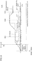
- Fig. 8 is a view describing the compression/decompression process of the edge code according to the embodiment of the present invention.
- Fig. 9 is a view showing results of the edge code extraction process along line IX-IX of the input image IMG shown in Fig. 8 .
- the input image IMG in which the target work is imaged will be considered.
- the edge code extraction process is executed along line IX-IX of the input image IMG shown in Fig. 8 .
- the valid edge code values are acquired near three edges EDG31, EDG2, EDG3.
- the edge code image configured by the edge code values on line IX-IX is obtained, as shown in Fig. 9 .
- the edge code value is invalid at a portion distant from the edges EDG1, EDG2, EDG3 of the input image IMG.
- the edge code value is less likely to greatly change at a small pixel interval in the input image obtained by imaging the target work.
- the direction of the edge that is, the contour of the target work, the structure of the surface, and the like need to physically change in order for the edge code value to greatly change, but the amount of change rate thereof is self-limited.
- the amount of information of the valid zone is diffused to the entire edge code image.
- the amount of information used in the entire edge code image is compressed by reducing the number of bits assigned to each pixel, and effectively using the number of bits assigned to each pixel as a whole.
- the image processing device 100 assigns the increase/decrease information from the edge code value contained in the valid zone for the edge EDG1 to the edge code value contained in the valid zone for the edge EDG2 to the element corresponding to the invalid zone when the valid zone for the edge EDG1 in which the valid edge code values continue, the invalid zone in which the invalid edge code values continue following the valid zone for the edge EDG1, and the valid zone for the edge EDG2 in which the valid edge code values continue following the invalid zone appear in the profile of the sequentially outputted edge code value.
- information for specifying the valid edge code value is assigned in correspondence to an element generated before the element having a valid edge code value and having an invalid edge code value.
- the differential image as shown in Fig. 9 is generated by sequentially calculating the difference in the edge code value between the adjacent elements of the edge code image.
- the differential image shows whether the edge code value in the element at a certain position is increasing or decreasing with respect to the edge code value of the element positioned one before.
- the amount of information assigned to each element is only 1 bit when such an differential image is used.
- the decompressed image as shown in Fig. 9 is obtained by storing the differential image in the memory and integrating along the input order of the differential images when performing the pattern matching process. The pattern matching process is then executed based on the decompressed image.
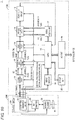
- Fig. 10 is a schematic view showing the hardware configuration of the pattern matching processing system 1 according to the embodiment of the present invention.
- the imaging device 200 includes a lens 21, an imaging element 22, an A/D (Analog to Digital) converter 23, and a control circuit 24, and outputs the input image (image signal) obtained by imaging the target work.
- A/D Analog to Digital
- the lens 21 is arranged on an optical axis entering the imaging element 22, and guides the reflected light from the subject to the imaging element 22 after being optically adjusted.
- the imaging element 22 typically includes a CCD (Coupled Charged Device), a CMOS (Complementary Metal Oxide Semiconductor) sensor, and the like, and outputs an image signal corresponding to the intensity of the incident light.
- the A/D converter 23 converts the image signal (analog signal) from the imaging element 22 to a digital signal.
- the A/D converter 23 typically samples the image signal from the imaging element 22 at a resolution of a predetermined number of bits, and outputs a corresponding digital value.
- the control circuit 24 is responsible for the overall control of the imaging process in the imaging device 200.
- the control circuit 24 includes a clock signal generation circuit 25 for generating a clock signal CL having a predetermined cycle.
- the readout of the image signal from the imaging element 22 and the A/D conversion process in the A/D converter 23 are periodically executed according to the clock signal CL generated by the clock signal generation circuit 25.
- the control circuit 24 gives a control command to the imaging element 22 to output the detected image signal along a predetermined scanning direction according to the clock signal CL. Therefore, the image information of each pixel contained in the input image is outputted in time-series along the predetermined scanning direction as an image signal from the A/D converter 23.
- the control circuit 24 outputs the image signal outputted from the A/D converter 23 to the image processing device 100.
- the control circuit 24 also outputs the clock signal CL generated by the clock signal generation circuit 25 to the image processing device 100.
- the input image may be a monochrome (grayscale) image or a color image
- the gray value represented by a predetermined number of bits typically, eight bits
- the gray value of the basic colors typically, red (R), green (G), blue (B)
- a predetermined number of bits typically, eight bits
- information representing the gray value of cyan (C), magenta (M), and yellow (Y). which are complementary colors of three primary colors of light may be used.
- the imaging device 200 has greater number of bands (sensitivity wavelength)
- the gray value of a number corresponding to the number of bands may be outputted.
- the image processing device 100 includes an EC (Edge Code) image generation circuit 11, a differential image generation circuit 12. an image decompression circuit 13, a difference calculation circuit 14, a peak hold circuit 15, an image memory 16, a model holding unit 17, a CPU (Central Processing Unit) 18, an I/O (Input/Output) port 19, and a display unit 20, and executes the pattern matching process on the input image acquired by the imaging device 200.
- the EC image generation circuit 11, the differential image generation circuit 12, the image decompression circuit 13, the difference calculation circuit 14, and the peak hold circuit 15 operate in synchronization with each other according to the clock signal CL.
- the EC image generation circuit 11 executes the edge extraction process (described later), based on the gray value of the input image received from the imaging device 200 to extract the edge and to specify the changing direction of the extracted edge.
- the EC image generation circuit 11 outputs the specified changing direction of the edge as an edge code value. More specifically, the EC image generation circuit 11 sequentially generates the "edge code value (EC value)" and the "valid/invalid flag” every time the gray value of each pixel for the input image is inputted.
- EC value edge code value
- the "valid/invalid flag" is the information of one bit indicating whether the corresponding edge code is valid or invalid.
- the differential image generation circuit 12 generates a differential image as shown in Fig. 9 based on a series of edge code values and the valid/invalid flag (and also edge code image) continuously outputted from the EC image generation circuit 11
- the (differential image has an element of the same number as the input image, but the amount of information assigned to each element is compressed from six bits to one bit.
- the differential image generation circuit 12 includes a storage unit for sequentially storing the edge code image (differential value and valid/invalid flag)after the compression. One part of the compressed edge code image stored in the storage unit is sequentially outputted to the image decompression circuit 13.
- the image decompression circuit 13 holds the compressed edge code image (differential value and valid/invalid flag) inputted in time-series by a predetermined element, and decompresses the held edge code image after the compression to the edge code image. The image decompression circuit 13 then provides the decompressed edge code image to the difference calculation circuit 14.
- the difference calculation circuit 14 performs the pattern matching process on the decompressed edge code image received from the image decompression circuit 13. In other words, the difference calculation circuit 14 calculates the similarity degree between the decompressed edge code image and the model image defined in advance. More specifically, the difference calculation circuit 14 reads out the edge code image (coordinate, as well as, edge code value and valid/invalid flag at each coordinate) representing the standard pattern (model image) registered in advance from the model holding unit 17, and compares the read edge code image of the model image and the decompressed edge code image provided from the difference calculation circuit 14. Furthermore, the difference calculation circuit 14 outputs the degree of similarly calculated by comparing the edge code images to the peak hold circuit 15.
- the peak hold circuit 15 holds the highest value (peak value) of the similarity degree outputted from the difference calculation circuit 14. In this case, the peak hold circuit 15 associates and holds the window position on the input image corresponding to the timing the peak value appeared based on the clock signal CL.
- the position of the window WN ( Fig. 4 ) set on the input image substantially moves one pixel at a time every time a new image signal worth one pixel contained in the input image is inputted to the image processing device 100,
- the portion having a high similarity degree with the model image that is, that matches the most with the model image can be specified by specifying the window position on the input image corresponding to the timing the peak value appeared.
- the CPU 18 is responsible for the overall control in the image processing device 100.
- the CPU 18 can use a ROM (Read Only Memory) for storing programs, and RAM (Random Access Memory) for work (both of which are not shown).
- the CPU 18 develops the program read out from the ROM on the RAM and executes the process.
- the image memory 16 is a storage region for temporarily storing the input image outputted from the imaging device 200, where the input image stored in the image memory 16 is typically displayed on the display unit 20 as a result of the pattern matching process in accordance with the position specified in the peak hold circuit 15.
- the I/O port 19 intermediates a data exchange between an external device connected to the image processing device 100 and the CPU 18.
- the display unit 20 displays or notifies the result of the pattern matching process in the image processing device 100.
- the display unit 20 typically includes a liquid crystal display, an LED (Light Emitting Diode), and the like.
- Fig. 11 is a block diagram showing a more detailed configuration of the EC image generation circuit 11 shown in Fig. 10 .
- the EC image generation circuit 11 includes a horizontal edge intensity detector 111, a vertical edge intensity detector 112, an EC value calculator 113, a quantizer 114, an edge intensity calculator 115, and a threshold value processor 116.
- the horizontal edge intensity detector 111 calculates the edge intensity in the horizontal direction based on the gray values of the adjacent pixels for each pixel contained in the input image provided from the imaging device 200 ( Fig. 10 ).
- the vertical edge intensity detector 112 calculates the edge intensity in the vertical direction based on the gray values of the adjacent pixels for each pixel contained in the input image provided from the imaging device 200 ( Fig. 10 ).
- a known method can be adopted for the configuration of calculating the edge intensity, but a maximum value of the difference in the gray values between the adjacent pixels may be assumed as the edge intensity.
- the horizontal edge intensity detector 111 and the vertical edge intensity detector 112 operate according to the clock signal CL, and respectively calculate the edge intensity every time a new pixel contained in the input image is inputted, and output the result to the EC value calculator 113 and the edge intensity calculator 115.
- the EC value calculator 113 outputs the calculated angle ⁇ to the quantizer 114.
- the following equation (1') may be used when defining the EC value in the range of between 0° and 180°.
- angle ⁇ tan ⁇ 1 B / A
- the quantizer 114 quantizes the angle ⁇ provided from the EC value calculator 113 to six bits, and outputs as the edge code value.
- the amount of information of the edge code value can be suppressed to the number of bits same as in the case of the monochrome image even if the color image having a greater number of bits is provided.
- the calculated edge code is valid is determined for the edge intensity calculator 115 and the threshold value processor 116. In other words, whether or not a sufficiently strong edge exists at the target position of the input image is determined based on the edge intensity, and the calculated edge code value is made valid at the relevant timing only if the edge having a predetermined intensity exists.
- the edge intensity calculator 115 calculates the edge intensity in each pixel of the input image according to the following equation (2) based on the horizontal edge intensity A calculated by the horizontal edge intensity detector 111 and the vertical edge intensity B calculated by the vertical edge intensity detector 112.
- Edge intensity ⁇ A 2 + B 2
- the threshold value processor 116 compares the edge intensity calculated by the edge intensity calculator 115 with a threshold value TH1 set in advance.
- the threshold value processor 116 outputs "1" indicating a valid value for the valid/invalid flag if the calculated edge intensity exceeds the threshold value TH1, and outputs "0" indicating an invalid value for the valid/invalid flag if the calculated edge intensity does not exceed the threshold value TH1.
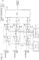
- Fig. 12 is a block diagram showing a more detailed configuration of the differential image generation circuit 12 shown in Fig. 10 .
- the (differential image generation circuit 12 includes flip-flops (FF) 121-1 to 121-4, 125, 126-1 to 126-4, a valid EC value extracting unit 122, a difference unit 123, an adder 124, and a valid pixel position specifying unit 127.
- FF flip-flops
- the flip-flops 121-1 to 121-4 are typical examples of delay elements connected in series, and sequentially shift the data in synchronization according to the clock signal CL.
- the edge code value generated by the EC image generation circuit 11 ( Fig. 10 ) is sequentially inputted to the input end of the flip-flop 121-4.
- the output end of the flip-flop 121-1 is connected to the valid EC value extracting unit 122.
- the edge code value at each input end of the flip-flops 121-1 to 121-4 is also inputted to the valid EC value extracting unit 122.
- an edge code value generated at time t by the EC image generation circuit 11 is represented as EC(t), and the time worth one cycle of the clock signal CL is represented as Dc.
- the EC(t-4Dc) is outputted from the flip-flop 121-1
- the EC(t-3Dc) is outputted from the flip-flop 121-2
- the EC(t-2Dc) is outputted from the flip-flop 121-3
- the EC(t-Dc) is outputted from the flip-flop 121-4.
- the flip-flops 121-1 to 121-4 coincide the timing for a plurality of continuous edge code values inputted at a different timing.
- the valid EC value extracting unit 122 outputs to the difference unit 123 one corresponding edge code value of the EC values (EC(t), EC(t-Dc), EC(t-2Dc), EC(t-3Dc), EC(t-4Dc)) respectively held by the flip-flops 121-1 to 121-4 according to a valid pixel position X specified by the valid pixel position specifying unit 127, to be described later.
- a valid pixel position X specified by the valid pixel position specifying unit 127, to be described later.
- the edge code value needs to be changed in advance after the termination of a certain valid zone and before the next valid zone appears, as shown by the decompressed image of Fig 9 .
- the valid pixel position specifying unit 127 foresees at which position the next valid zone appears. Specifically, the valid pixel position specifying unit 127 outputs that having the smallest value of X holding the valid edge code value of the series of flip-flops 121-1 to 121-4 as the valid pixel position X.
- the valid EC value extracting unit 122 outputs the edge code value held by the corresponding flip-flop 121 according to the extracted valid pixel position X.
- the flip-flops 126-1 to 126-4 are typical examples of delay elements connected in series, and sequentially shift the data in synchronization according to the clock signal CL.
- the valid/invalid flag value generated by the EC image generation circuit 11 ( Fig. 10 ) is sequentially inputted to the input end of the flip-flop 126-4.
- the output end of the flip-flop 126-1 is connected to the valid pixel position specifying unit 127.
- the valid/invalid flag value at each input end of the flip-flops 126-1 to 126-4 is also inputted to the valid pixel position specifying unit 127.
- the valid pixel position specifying unit 127 specifies that having the smallest value of the corresponding valid pixel position X of those in which the value is "1" indicating valid of the inputted valid/invalid flag values. The valid pixel position specifying unit 127 then outputs the specified value of X to the valid EC value extracting unit 122. If all of the inputted valid/invalid flag values are "0" , the valid pixel position specifying unit 127 outputs "4" as the valid pixel position X.
- the difference unit 123 compares a magnitude relationship of the edge code value (current value) outputted from the valid EC value extracting unit 122 and the edge code value (previous value) in the cycle one before the relevant cycle in each cycle of the clock signal CL, and outputs a differential, value (one bit) based on the difference as the increase/decrease information. In other words, the difference unit 123 outputs "1", which means increase in terms of differential value, if the edge code value (current value) is greater than the edge code value (previous value), and outputs "0", which means decrease in terms of differential value, if the edge code value (current value) is not greater than the edge code value (previous value).
- the adder 124 and the flip-flop 125 are circuits for calculating the edge code value (previous value).
- the adder 124 calculates a new edge code value (previous value) by adding or subtracting "one bit" to the edge code value (previous value) outputted from the flip-flop 125 according to the differential value outputted from the difference unit 123.
- the new edge code value (previous value) calculated by the adder 124 is provided to, and held by the flip-flop 125.
- the new edge code value (previous value) provided from the adder 124 to the flip-flop 125 is used as the edge code value (previous value) in the next clock cycle.
- the number of connecting stages of the flip-flops 121 and 126 shown in Fig. 12 corresponds to the number of elements (number of pixels) for foreseeing the valid zone that appears next. Therefore, a great number of stages (e.g., 16 stages or 32 stages) is preferably provided so that the foreseeing amount is preferably increased, and the information on the valid edge code value in the original edge code image can be compressed/decompressed at high accuracy.
- the edge code image can be more accurately compressed even if the foreseeing accuracy is relatively low by assigning a greater amount of information to the differential value (differential image) that is the increase/decrease information.
- Fig. 13 is a block diagram showing a more detailed configuration of the image decompression circuit 13 shown in Fig. 10 .
- the image decompression circuit 13 includes a shift register 131, a delay unit 132, and a decompression unit 133.
- a plurality of shift registers 131 is series-connected in sequence, and sequentially stores the differential value and the valid/invalid flag provided from the differential image generation unit 12 ( Fig. 10 ) in FIFO.
- One shift register 131 typically has a storage capacity of storing the differential value and the valid/invalid flag worth one horizontal line.
- each shift register 131 has a memory capacity of 2 ⁇ W ⁇ H (bit) if the input image has a size of W pixels ⁇ H lines.
- the differential image for one input image can be temporarily stored by preparing the shift register 131 by the number same as the number of lines of the input image.
- the storage capacity of the shift register 131 can be reduced to 1/4 in simple calculation compared to when storing a monochrome image in which each element is defined with a gray value of eight bits as is.
- a set of the delay unit 132 and the decompression unit 133 is arranged by the number of evaluation devices for performing the pattern matching process in the window set in the input image. In other words, the pattern matching process based on the edge code is performed in each set of the delay unit 132 and the decompression unit 133.
- n sets of the delay unit 132 and the decompression unit 133 are arranged in the horizontal direction, and m sets of the delay unit 132 and the decompression unit 133 are arranged in the vertical direction.
- This arrangement means that m evaluation lines can be set in the window, and n evaluation positions can be set on each evaluation line.
- the delay unit 132 is connected to the output end of each shift register 131.
- Fig. 14 is a schematic view showing one example of a model image registered in the image processing device according to the embodiment of the present invention.
- an input image IMG is acquired by imaging a standard work, which becomes a reference of the pattern matching process.
- a window WN is set in a range to be the model image in the input image IMG.
- a plurality of edge codes used in the pattern matching process is extracted from the partial image in the window WN.
- m evaluation lines L0, L1, ..., L(m-1) are set with respect to the window WN, and the edge code is calculated on each evaluation line.
- the valid edge code is extracted at a coordinate point P1 on the evaluation line L0, and the valid edge code is extracted at coordinates P2 and P3 on the evaluation line L1.
- the valid edge codes are also extracted on the remaining evaluation lines.
- the coordinate P1 is at a position spaced apart by a distance d1 from the left end of the window WN, and the coordinate P2 is at a position spaced apart by a distance d2 from the coordinate P1.
- the similarity degree may be evaluated at the respective coordinates where the valid edge codes are extracted.
- the position (coordinate) of the pixel where the valid edge code is not extracted on a certain evaluation line does not need to be the target of evaluation. Therefore, at which position the similarity degree with the edge code is to be evaluated on each evaluation fine needs to be registered in advance.
- the model image is defined using the relative positional information indicating the difference in the relative positions between the adjacent evaluation positions on the same evaluation line.
- Such relative positional information uses "number of delays” indicating the number of elements that exists between the adjacent evaluation positions.
- a configuration for extracting the differential value (or edge code value to be decompressed) at a coordinate spaced apart by such "number of delays" on the same evaluation line is the delay unit 132 shown in Fig. 13 .
- the differential value at each evaluation position registered in advance is then outputted to the decompression unit 133 through the delay unit 132.
- the edge code value is decompressed from the differential value at each evaluation position in the decompression unit 133.
- Fig. 15 is a block diagram showing a more detailed configuration of the delay unit 132 shown in Fig. 13 .
- the delay unit 132 includes flip-flops (FF) 1321-1, 1321-2, ..., 1321-k, and a selector (SEL) 1322.
- FF flip-flops
- SEL selector
- the flip-flop 1321-1 to 1321-k are typical examples of delay elements connected in series, and sequentially shift the data in synchronization according to the clock signal CL.
- the value same as the differential value and the valid/invalid flag held at a predetermined position of the shift register 131 ( Fig. 13 ) (connection node of adjacent shift register 131) is sequentially inputted to the input end of the flip-flop 1321-1.
- the respective output ends of the flip-flops 1321-1 to 1321-k are connected to the selector 1322.
- the selector 1322 is typically configured with a multiplexer.
- the selector 1322 outputs one of the outputs of the flip-flops 1321-1 to 1321-k to the delay unit 132 and the corresponding decompression unit 133 connected to the post-stage according to the corresponding number of delays stored in the model holding unit 17, to be described later.
- the selector 1322 selects the output of the flip-flop 1321-1.
- the delay amount between the target delay unit 132 and the delay unit 132 connected to the pre-stage thereof is worth one pixel. Therefore, the coordinate spaced apart by one pixel on the target evaluation line of the input image from the evaluation position, which is the target for the set of the delay unit 132 and the decompression unit 133 connected at the pre-stage, is set as the evaluation position.
- the target evaluation position on the same evaluation line can be freely set by setting the number of delays according to the model image.
- Fig. 16 is a block diagram showing a more detailed configuration of the decompression unit 133 shown in Fig. 13 .
- the decompression unit 133 includes an adder 1331, a flip-flop (FF) 1332, and a timing adjuster 1333.
- FF flip-flop
- the adder 1331 and the flip-flop 1332 are an integration circuit for calculating the edge code decompression value from the differential value.
- the adder 1331 calculates the edge code decompression value (current value) by adding "+1" or "-1" to the edge code decompression value (previous value) outputted from the flip-flop 1332 according to the differential value outputted from the corresponding delay unit 132 ( Fig. 15 ),
- the edge code decompression value (current value) calculated by the adder 1331 is provided to, and held by the flip-flop 1332, and also outputted to the difference calculation circuit 14 arranged at the post-stage.
- the edge code decompression value (current value) provided to the flip-flop 1332 is used as the edge code decompression value (previous value) in the next clock cycle.
- the timing adjuster 1333 resets the flip-flop 1332 at the timing defined in advance. Since the edge code decompression value is typically calculated for every horizontal line of the input image, the calculation of the edge code decompression value on the next horizontal line may not be influenced after the calculation of the edge code decompression value for a certain horizontal line is completed.
- the timing adjuster 1333 outputs a reset signal to the flip-flop 1332 at the timing of the horizontal blank period, and clears the integration value held by the flip-flop 1332 to zero.
- the resetting is not necessarily required by the timing adjuster 1333.
- the "edge code (EC) decompression value” and the “valid/invalid flag value” for the corresponding evaluation position are outputted from each set of delay unit 132 and decompression unit 133.
- Fig. 17 is a block diagram showing a more detailed configuration of the difference calculation circuit 14 shown in Fig. 10 .
- Figs. 18A and 18B are views showing one example of a data structure held by the model holding unit 17 shown in Fig. 10 .
- Fig. 19 is a view schematically showing an angle indicating the edge code value shown in Figs. 18A and 18B .
- the difference calculation circuit 14 includes a plurality of difference units 141, a determination unit 142 corresponded with each difference unit 141, and an adder 143.
- Each set of the difference unit 141 and the determination unit 142 determines success and fail of pattern matching at the evaluation position by comparing the edge code decompression value and the valid/invalid flag provided from the decompression unit 133 ( Fig. 16 ) arranged at the pre-stage, and the corresponding edge code value and the value of the valid/invalid flag read out from the model holding unit 17.
- the adder 143 adds up the result outputted from each set of the difference unit 141 and the determination unit 142, and outputs the added result to the peak hold circuit 15 ( Fig. 10 ) as the similarity degree by pattern matching.
- each difference unit 141 calculates a difference value (L1, L2, ..., Li) of the edge code decompression value from the decompression unit 133 arranged at the pre-stage, and the corresponding edge code value read out from the model holding unit 17.
- Each determination unit 142 outputs, to the adder 143, "1" that means matching is successful at the corresponding evaluation position when both of (1) absolute value of the difference value provided from the difference unit 141 arranged at the pre-stage is smaller than the threshold TH2, and (2) the corresponding valid/invalid flag read out from the model holding unit 17 is "1" are satisfied. If (1) or (2) is not satisfied, the determination unit 142 outputs, to the adder 143, "0" that means matching has failed at the corresponding evaluation position.
- condition of (1) is a condition for determining that matching is successful only when the value of the edge code at the evaluation position in the window set on the input image is the same or approximate to the value of the edge code at the corresponding evaluation position of the model image.
- condition of (2) is a condition for excluding the result calculated for the coordinate that is not the original evaluation position since the position that is not the original evaluation position is sometimes set as the evaluation position in the model holding unit 17, as described later.
- the model holding unit 17 stores three parameters "valid/invalid flag”, “edge code (EC) value”, and "number of delays" for each evaluation position set on the model image.
- the set values shown in Fig. 18A correspond to the model image shown in Fig. 14 .
- the "valid/invalid flag” is set with either "0" indicating that the corresponding evaluation position is invalid, or "1" indicating that the corresponding evaluation position is valid.
- the "EC value” is set with a value (i.e., 0 to 63) in which the value of the edge code at the corresponding evaluation position is quantized to six bits.
- the "number of delays” is set with a positive integer having the number of steps of the flip-flops 1321-1, 1321-2 to 1321-k contained in the delay unit 132 shown in Fig. 15 as a maximum value.
- Figs. 18A and 18B illustrate a case in which the delay unit 132 includes the flip-flops 1321 connected in series in eight stages. In other words, the number of stages of the flip-flops 1321 contained in the delay unit 132 becomes the maximum value of the degree of delays that can be set.
- the edge code is "90°” when the quantized edge code value is "15”
- the edge code is "180°” when the quantized edge code value is "31”
- the edge code is "270°” when the quantized edge code value is "47”.
- the evaluation line L1 will be considered with reference to Fig. 14 again.
- the number of delays d1 from the left end of the window WN to the coordinate P2 is "20”
- the number of delays d2 from the coordinate P2 to the coordinate P3 is "16”.
- the maximum number of delays that can be set with respect to one delay unit 132 is "8” if the flip-flops 1321 configuring the delay unit 132 is eight stages.
- the necessary number of delays "20" is realized by using a plurality of delay units 132.
- the number of delays "8" is set with respect to the delay unit 132 at the most pre-stage (intersection of L1 and X0 in the table of Fig. 18A ), the number of delays "8” is also set with respect to the following delay unit 132 of the second stage (intersection of L1 and X1 in the table of Fig. 18A ), and the number of delays "4" is set with respect to the following delay unit 132 of the third stage (intersection of L1 and X2 in the table of Fig. 18A ). Since the delay units 132 of the first stage and the second stage are not original evaluation positions, the valid/invalid flag of the corresponding parameters is set to "0". Since the delay unit 132 of the third stage is the original evaluation position, the valid/invalid flag of the corresponding parameters is set to "1" and the extracted edge code value is set.
- the parameter representing the characteristics of the model image is similarly registered in the model holding unit 17.
- the cell with hatching in the table shown in Fig. 18A corresponds to the evaluation position shown in Fig. 14 .
- Fig. 20 is a flowchart showing the processing procedure of the model registration according to the embodiment of the present invention.
- the processing procedure shown in Fig. 20 is implemented when the CPU 18 shown in Fig. 10 executes the program.
- the processing procedure may be executed with the image processing device of a different body from the image processing device 100 according to the present embodiment.
- the CPU 18 calculates the profile of the edge intensity on the evaluation line corresponding to the line number variable k (step S108). In other words, the CPU 18 calculates the edge intensity at the position of each pixel on the evaluation line. Furthermore, the CPU 18 extracts a maximum point in the profile of the calculated edge intensity (step S110), and calculates the edge code value at each maximum point (step S112). Assuming n maximum points are extracted, the coordinate and the edge code value at the respective maximum point are (x0, y0: c0), (x2, y2, c2), ⁇ , (x(n-1), y(n-1) ;c(n-1)). The maximum point number is assigned to 0 to (n-1) from the number closest to the origin position on the X-axis.
- the CPU 18 determines whether or not the number variable j after the update is smaller than n, i.e., the number of extracted maximum points (step S128). If the number variable j is smaller than n (YES in step S128), the process returns to step S116.
- step S1208 If the number variable j is greater than or equal to n (NO in step S128), the CPU 18 adds "1" to the line number variable k to update to a new line number variable k (step S130). Furthermore, the CPU 18 determines whether or not the line number variable k after the update is smaller than m, i.e., the number of set evaluation lines (step S132), If the line number variable k is smaller than m (YES in step S132), the process returns to step S108.
- step S132 If the line number variable k is greater than or equal to m (NO in step S132), the registration process is terminated.
- the processing procedure in the image processing device 100 according to the present embodiment is summarized in a flowchart of Fig. 21 .
- Fig. 21 is a flowchart showing the processing procedure in the pattern matching processing system 1 according to the embodiment of the present invention. The processes shown in Fig. 21 are repeatedly executed at the cycle of the clock signal CL.
- the imaging device 200 outputs image information (gray value) on one pixel contained in the input image obtained by imaging to the image processing device 100 (step S2).
- the horizontal edge intensity detector 111 and the vertical edge intensity detector 112 of the image processing device 100 calculate the edge intensity in the horizontal direction and the vertical direction, respectively (step S4). Since the edge intensity needs to be calculated based on the gray value at the target pixel and the surrounding pixels thereof, the process of step S4 is skipped if the surrounding pixels are not inputted.
- the EC value calculator 113 of the image processing device 100 calculates the angle ⁇ indicating the changing direction of the edge based on the edge intensities in the horizontal direction and the vertical direction calculated in step S4 (step S6).
- the angle ⁇ calculated by the EC value calculator 113 of the image processing device 100 ( Fig. 11 ) is then quantized to calculate the edge code value (step S8).
- the edge intensity calculator 115 of the image processing device 100 calculates the edge intensity on the pixel to become the target based on the edge intensities in the horizontal direction and the vertical direction calculated in step S4 (step S10).
- the threshold value processor 116 of the image processing device 100 compares the calculated edge intensity and the threshold value TH1 to determine the value of the valid/invalid flag (step S12).
- the differential image generation circuit 12 provides the edge code value calculated in step S8 to the flip-flop 121-4 ( Fig. 12 ) and shifts the data held by the flip-flops 121-1 to 121-4, and also provides the value of the valid/invalid flag determined in step S12 to the flip-flop 126-4 ( Fig. 12 ) and shifts the data held by the flip-flops 126-1 to 126-4 (step S14).
- the valid pixel position specifying unit 127 of the differential image generation circuit 12 ( Fig. 12 ) then specifies the position of the flip-flop having the valid/invalid flag value of "1'' of the flip-flops 126-1 to 126-4 as a valid pixel position X (step S16).
- the valid EC value extracting unit 122 of the differential image generation circuit 12 extracts the edge code value held by the flip-flop corresponding to the valid pixel position X specified in step S16 of the flip-flops 121-1 to 121-4 (step S18).
- the difference unit 123 of the differential image generation circuit 12 calculates the (differential value based on a difference between the edge code value (current value) extracted in step S18 and the edge code value (previous value) extracted in the previous processing cycle (step S20).
- the image decompression circuit 13 ( Fig. 13 ) provides the edge code value calculated in step S20 and the value of the valid/invalid flag shifted in step S14 to the shift register 131, and shifts the data held by the shift register 131 (step S22.
- each delay unit 132 provides the edge code value and the value of the valid/invalid flag held after being shifted in the shift register 131 of the connecting destination to the flip-flop 1321-1 ( Fig. 15 ), and shifts the data held by the flip-flops 1321-1 to 1321-k (step S24).
- the selector 1322 of each delay unit 132 selects one of the flip-flops 1321-1 to 1321-k and outputs the value being held according to the corresponding number of delays stored in the model holding unit 17 (step S26).
- Each decompression unit 133 of the image decompression circuit 13 adds the differential value (current value) outputted from the selector 1322 of the corresponding delay unit 132 in step S26, and the edge code decompression value (previous value) calculated in the previous processing cycle, and calculates the edge code decompression value (current value) (step S28).
- the difference calculation circuit 14 receives the edge code decompression value calculated by a plurality of decompression units 133 of the image decompression circuit 13 in step S28, calculates the similarity degree with the model image defined in advance, and outputs to the peak hold circuit 15 ( Fig. 10 ) (step S30). The process in the current clock cycle is then terminated.
- step S2 When the next clock cycle arrives, the processes after step S2 are again executed.
- the edge code image generated based on the gray value of the input image is sequentially stored in the line buffer after being compressed, and thus the necessary storage region can be reduced compared to a case where the edge code image is stored as is in the line buffer.
- the pattern matching based on the edge code thus can be implemented with a smaller circuit configuration.
- compression is carried out using the increase/decrease information (i.e., differential value) of the edge code value between the adjacent elements in the edge code image, and thus decompression to the edge code value can be carried out by simply integrating the differential value in time-series.
- decompression to the edge code image can be carried out within one clock cycle.
- the circuit configuration for decompressing the compressed edge code image can be simplified, and the decompression process can be carried out in a short time.
- the real time processing in which the pattern matching process completes at a time substantially similar to the time required to acquire one input image can be realized.
- a configuration of decompressing the differential image to the edge code image and performing the pattern matching process with the model has been illustrated, but a model image corresponding to the differential image may be registered in advance, and the pattern matching process may be performed with the input image compressed to a differential image.
- each element of the edge code image independently includes the edge code value and the valid/invalid flag has been illustrated, but a data structure of an integrated form may be adopted.
- data of seven bits may be assigned to each element of the edge code image, a range the data of seven bits may take may be set, for example, to a range of (-1 to 126), and invalid may be indicated when "-1".
Landscapes
- Engineering & Computer Science (AREA)
- Theoretical Computer Science (AREA)
- Physics & Mathematics (AREA)
- General Physics & Mathematics (AREA)
- Multimedia (AREA)
- Computer Vision & Pattern Recognition (AREA)
- Software Systems (AREA)
- Artificial Intelligence (AREA)
- Health & Medical Sciences (AREA)
- Computing Systems (AREA)
- Databases & Information Systems (AREA)
- Evolutionary Computation (AREA)
- General Health & Medical Sciences (AREA)
- Medical Informatics (AREA)
- Image Analysis (AREA)
- Image Processing (AREA)
- Compression Or Coding Systems Of Tv Signals (AREA)
- Compression Of Band Width Or Redundancy In Fax (AREA)
Claims (9)
- Bildverarbeitungsvorrichtung (100) für einen Musterabgleich, die Folgendes umfasst:eine Generierungseinheit (11), die dafür konfiguriert ist, ein Kantencodebild auf der Basis eines Grauwertes eines eingegebenen Bildes zu generieren, wobei jedes in dem Kantencodebild enthaltene Element einen Kantencodewert und Informationen enthält, die anzeigen, ob der Kantencodewert gültig oder ungültig ist, wobei jedes Element einem einzelnen in dem eingegebenen Bild enthaltenen Pixel entspricht, wobei der Kantencodewert einem gültigen Pixel entspricht, wenn eine Kante an dem Pixel detektiert wird;eine Komprimierungseinheit (12), die dafür konfiguriert ist, das Kantencodebild zu komprimieren, indem einem Element, das einen ungültigen Kantencodewert besitzt, Informationen zugewiesen werden, die den Kantencodewert für ein Element darstellen, das einen gültigen Kantencodewert besitzt;eine Speichereinheit (131), die dafür konfiguriert ist, das komprimierte Kantencodebild der Reihe nach zu speichern;eine Dekomprimierungseinheit (13), die dafür konfiguriert ist, das in der Speichereinheit (131) gespeicherte komprimierte Kantencodebild zu dekomprimieren; undeinen Komparator (14), der dafür konfiguriert ist, den Musterabgleich durch Berechnen eines Ähnlichkeitsgrades zwischen dem durch die Dekomprimierungseinheit (13) dekomprimierten Kantencodebild und einem im Voraus definierten Modellbild auszuführen,wobei die Komprimierungseinheit (12) dafür konfiguriert ist, den in jedem zuvor festgelegten Zyklus durch die Generierungseinheit (11) generierten Kantencodewert und die Informationen, die anzeigen, ob der Kantencodewert gültig oder ungültig ist, über mehrere Verarbeitungszyklen hinweg zu halten und einen Differenzialwert als eine Erhöhungsinformation auszugeben, falls der Kantencodewert in einem momentanen Zyklus größer ist als der Kantencodewert in einem vorherigen Zyklus, und anderenfalls als eine Verringerungsinformation auszugeben, unddie Dekomprimierungseinheit dafür konfiguriert ist, das komprimierte Kantencodebild durch Integrieren der erhaltenen Differenzialwerte zu dekomprimieren.
- Bildverarbeitungsvorrichtung (100) nach Anspruch 1, wobeiin die Generierungseinheit (11) der Grauwert eines jeden in dem eingegebenen Bild enthaltenen Pixels in einer vorgegebenen Reihenfolge eingespeist wird;die Generierungseinheit (11) der Reihe nach den Kantencodewert für jede Eingabe des Grauwert generiert; unddie Komprimierungseinheit (12) Informationen zum Spezifizieren des gültigen Kantencodewertes in Entsprechung zu einem Element ausgibt, das vor einem Element mit einem gültigen Kantencodewert generiert wird und das einen ungültigen Kantencodewert hat.
- Bildverarbeitungsvorrichtung (100) nach Anspruch 1, wobei,wenn eine erste Zone (EGD1), in der sich der gültige Kantencodewert fortsetzt, eine zweite Zone, die der ersten Zone (EGD1) folgt, in der sich der ungültige Kantencodewert fortsetzt, und eine dritte Zone (EGD2),die der zweiten Zone folgt, in der sich der gültige Kantencodewert fortsetzt, in einem Profil des der Reihe nach ausgegebenen Kantencodewertes erscheinen,die Komprimierungseinheit (12) Erhöhungs-/verringerungs-Informationen von dem in der ersten Zone (EGD1) enthaltenen Kantencodewert zu dem in der dritten Zone (EGD2) enthaltenen Kantencodewert in Entsprechung zu einem Element, das der zweiten Zone entspricht, ausgibt.
- Bildverarbeitungsvorrichtung (100) nach einem der Ansprüche 1 bis 3, wobei die Komprimierungseinheit (12) Folgendes enthält:mehrere in Reihe verbundene erste Verzögerungselemente (121-1, 121-2, 121-3, 121-4), in die der Reihe nach die durch die Generierungseinheit (11) generierten Kantencodewerte in einem vorgegebenen Zyklus eingespeist werden,mehrere in Reihe verbundene zweite Verzögerungselemente (126-1, 126-2, 126-3, 126-4), in die der Reihe nach in dem vorgegebenen Zyklus die Informationen eingespeist werden, die anzeigen, ob der durch die Generierungseinheit (11) generierte Kantencodewert gültig oder ungültig ist,eine Positionsspezifizierungseinheit (127) zum Spezifizieren einer Position des zweiten Verzögerungselements, das Informationen speichert, die die Gültigkeit von Informationen anzeigen, die anzeigen, ob der in den mehreren zweiten Verzögerungselementen (126-1, 126-2, 126-3, 126-4) gehaltene Kantencodewert gültig oder ungültig ist,eine Extraktionseinheit (122) zum Extrahieren des in dem ersten Verzögerungselement gehaltenen Kantencodewertes, welcher der durch die Positionsspezifizierungseinheit (127) spezifizierten Position der in den mehreren ersten Verzögerungselementen (121-1, 121-2, 121-3, 121-4) gehaltenen Kantencodewerte entspricht, undeine Differenzberechnungseinheit (123), um der Reihe nach eine Differenz zwischen dem durch die Extraktionseinheit (12) in einem vorherigen Zyklus extrahierten Kantencodewert und dem durch die Extraktionseinheit (12) in einem momentanen Zyklus extrahierten Kantencodewert als die Erhöhungs-/Verringerungs-Informationen auszugeben.
- Bildverarbeitungsvorrichtung (100) nach Anspruch 4, wobei die Dekomprimierungseinheit (13) einen Integrationsabschnitt (1331, 1332) zum Integrieren der der Reihe nach ausgegebenen Erhöhungs-/Verringerungs-Informationen enthält.
- Bildverarbeitungsvorrichtung (100) nach Anspruch 5, wobeidie Dekomprimierungseinheit (13) Folgendes enthält:mehrere in Reihe verbundene dritte Verzögerungselemente (1321-1, 1321-2, ..., 1312-k), in die der Reihe nach in dem vorgegebenen Zyklus der an einer vorgegebenen Position der Speichereinheit (131) gehaltene Kantencodewert eingespeist wird, undeine Auswahleinheit (1332) zum Ausgeben, an den Integrationsabschnitt (1331, 1332), des in dem Verzögerungselement gehaltenen Kantencodewertes, der Relativpositionsinformationen entspricht, die in dem Modellbild der mehreren dritten Verzögerungselemente (1321-1, 1321 -2, ..., 1312-k) enthalten sind.
- Bildverarbeitungsvorrichtung (100) nach Anspruch 6, wobei das Modellbild einen Kantencodewert an einer Beurteilungsposition zum Berechnen des Ähnlichkeitsgrades enthält, und die Relativpositionsinformationen eine Differenz einer relativen Position zwischen der Beurteilungsposition und einer anderen Beurteilungsposition anzeigen.
- Bildverarbeitungsvorrichtung (100) nach einem der Ansprüche 1 bis 3, wobei die Generierungseinheit (11) Folgendes enthält:einen Detektor (111, 112) zum Detektieren einer Kantenintensität an jedem Pixel des eingegebenen Bildes; undeine Bestimmungseinheit (116) zum Ausgeben von Informationen, die anzeigen, dass der entsprechende Kantencodewert gültig ist, wenn die durch den Detektor detektierte Kantenintensität einen vorgegebenen Wert übersteigt.
- Bildverarbeitungsverfahren für einen Musterabgleich, das folgende Schritte umfasst:Generieren eines Kantencodebildes auf der Basis eines Grauwertes eines eingegebenen Bildes, wobei jedes in dem Kantencodebild enthaltene Element einen Kantencodewert und Informationen enthält, die anzeigen, ob der Kantencodewert gültig oder ungültig ist, wobei jedes Element einem einzelnen in dem eingegebenen Bild enthaltenen Pixel entspricht, wobei der Kantencodewert einem gültigen Pixel entspricht, wenn eine Kante an dem Pixel detektiert wird (S8, S12);Komprimieren des Kantencodebildes durch Zuweisen von Informationen, die den Kantencodewert für ein Element darstellen, das einen gültigen Kantencodewert besitzt, zu einem Element, das einen ungültigen Kantencodewert besitzt;Speichern, der Reihe nach, des komprimierten Kantencodebildes (S22);Dekomprimieren des gespeicherten komprimierten Kantencodebildes (S28); undAusführen des Musterabgleichs durch Berechnen eines Ähnlichkeitsgrades zwischen dem dekomprimierten Kantencodebild und einem im Voraus definierten Modellbild (S30),wobei der Schritt des Komprimierens des Kantencodebildes folgende Schritte enthält: Halten des in jedem zuvor festgelegten Zyklus in dem Generierungsschritt generierten Kantencodewertes und der Informationen, die anzeigen, ob der Kantencodewert gültig oder ungültig ist, über mehrere Verarbeitungszyklen hinweg (S14), und Ausgeben eines Differenzialwertes als eine Erhöhungsinformation, falls der Kantencodewert in einem momentanen Zyklus größer ist als der Kantencodewert in einem vorherigen Zyklus, und anderenfalls als eine Verringerungsinformation (S20); undwobei das gespeicherte komprimierte Kantencodebild durch Integrieren der erhaltenen Differenzialwerte dekomprimiert wird.
Applications Claiming Priority (1)
| Application Number | Priority Date | Filing Date | Title |
|---|---|---|---|
| JP2009061066A JP5212195B2 (ja) | 2009-03-13 | 2009-03-13 | 画像処理装置および画像処理方法 |
Publications (3)
| Publication Number | Publication Date |
|---|---|
| EP2228753A2 EP2228753A2 (de) | 2010-09-15 |
| EP2228753A3 EP2228753A3 (de) | 2013-11-20 |
| EP2228753B1 true EP2228753B1 (de) | 2017-08-23 |
Family
ID=42246091
Family Applications (1)
| Application Number | Title | Priority Date | Filing Date |
|---|---|---|---|
| EP10154035.9A Not-in-force EP2228753B1 (de) | 2009-03-13 | 2010-02-18 | Bildverarbeitungsvorrichtung und Bildverarbeitungsverfahren |
Country Status (3)
| Country | Link |
|---|---|
| US (1) | US8611679B2 (de) |
| EP (1) | EP2228753B1 (de) |
| JP (1) | JP5212195B2 (de) |
Families Citing this family (4)
| Publication number | Priority date | Publication date | Assignee | Title |
|---|---|---|---|---|
| JP2011247957A (ja) * | 2010-05-24 | 2011-12-08 | Toshiba Corp | パターン検査方法および半導体装置の製造方法 |
| JP5521975B2 (ja) * | 2010-10-25 | 2014-06-18 | セイコーエプソン株式会社 | 電気泳動表示装置の駆動方法、制御回路、および電気泳動表示装置 |
| CN106204661B (zh) * | 2016-06-23 | 2020-05-05 | 海信视像科技股份有限公司 | 图片有效性识别方法、装置及智能终端 |
| CN114693707B (zh) * | 2020-12-31 | 2023-09-26 | 北京小米移动软件有限公司 | 物体轮廓模板获取方法、装置、设备及存储介质 |
Family Cites Families (11)
| Publication number | Priority date | Publication date | Assignee | Title |
|---|---|---|---|---|
| DE2220624A1 (de) * | 1972-04-27 | 1973-11-08 | Licentia Gmbh | Verfahren zur erkennung von linienfoermigen mustern |
| FR2590703B1 (fr) * | 1985-11-25 | 1991-03-29 | Commissariat Energie Atomique | Procede de reconnaissance de caracteres en temps reel, notamment sur des objets en defilement rapide |
| US4961231A (en) * | 1987-01-20 | 1990-10-02 | Ricoh Company, Ltd. | Pattern recognition method |
| US5058181A (en) * | 1989-01-25 | 1991-10-15 | Omron Tateisi Electronics Co. | Hardware and software image processing system |
| DE69330813T2 (de) | 1992-03-06 | 2002-06-13 | Omron Corp., Kyoto | Bildprozessor und verfahren dafuer |
| JP3464308B2 (ja) * | 1995-03-28 | 2003-11-10 | 富士フイルムマイクロデバイス株式会社 | 画像圧縮装置 |
| JP2000101972A (ja) * | 1998-09-21 | 2000-04-07 | Sony Corp | 映像信号記録装置及び映像信号再生装置 |
| JP2002140713A (ja) * | 2000-11-02 | 2002-05-17 | Omron Corp | 画像処理方法およびその装置 |
| JP4023096B2 (ja) * | 2001-02-05 | 2007-12-19 | オムロン株式会社 | 画像処理方法およびその装置 |
| US6895104B2 (en) * | 2001-02-16 | 2005-05-17 | Sac Technologies, Inc. | Image identification system |
| JP4679425B2 (ja) * | 2006-04-20 | 2011-04-27 | 株式会社東芝 | 画像処理装置、画像処理方法およびプログラム |
-
2009
- 2009-03-13 JP JP2009061066A patent/JP5212195B2/ja not_active Expired - Fee Related
-
2010
- 2010-02-18 EP EP10154035.9A patent/EP2228753B1/de not_active Not-in-force
- 2010-02-25 US US12/712,913 patent/US8611679B2/en active Active
Non-Patent Citations (1)
| Title |
|---|
| None * |
Also Published As
| Publication number | Publication date |
|---|---|
| EP2228753A3 (de) | 2013-11-20 |
| JP2010217990A (ja) | 2010-09-30 |
| US20100232707A1 (en) | 2010-09-16 |
| EP2228753A2 (de) | 2010-09-15 |
| US8611679B2 (en) | 2013-12-17 |
| JP5212195B2 (ja) | 2013-06-19 |
Similar Documents
| Publication | Publication Date | Title |
|---|---|---|
| US8417059B2 (en) | Image processing device, image processing method, and program | |
| US11272163B2 (en) | Image processing apparatus and image processing method | |
| US10805528B2 (en) | Image capturing apparatus, information processing system, information processing apparatus, and polarized-image processing method | |
| EP3477582B1 (de) | Verfahren und system zur verarbeitung eines pixelstroms. | |
| US10057554B2 (en) | Projection control device, projection control method and non-transitory storage medium | |
| EP2228753A2 (de) | Bildverarbeitungsvorrichtung und Bildverarbeitungsverfahren | |
| US20200145641A1 (en) | Image processing apparatus and method | |
| JP6362632B2 (ja) | 画像処理装置、画像処理方法 | |
| US11551462B2 (en) | Document scanning system | |
| US6259813B1 (en) | Method and apparatus for image processing using a signal of multiple scale values | |
| JPH11220650A (ja) | 階調パターン整合による動き検出装置及びその方法 | |
| US8035703B2 (en) | Device and method for measuring noise characteristics | |
| US8526738B2 (en) | Information processing apparatus including a plurality of multi-stage connected information processing units | |
| US9167175B2 (en) | Flicker detection method and flicker detection apparatus | |
| EP3477584A1 (de) | Systeme und verfahren zur verarbeitung eines stroms von datenwerten | |
| US20150055825A1 (en) | Object detection apparatus and storage medium | |
| WO2018037479A1 (ja) | 画像処理装置、ステレオカメラ装置及び画像処理方法 | |
| EP3404534A1 (de) | Bedingter fluss mit hardwarebeschleunigung | |
| US9977992B2 (en) | Identifying points of interest in an image | |
| EP3933341A1 (de) | Berechnungsvorrichtung und parallaxenberechnungsverfahren | |
| JP5754931B2 (ja) | 画像解析装置、画像解析方法及びプログラム | |
| US9389731B2 (en) | Optical touch system having an image sensing module for generating a two-dimensional image and converting to a one-dimensional feature | |
| JP4144752B2 (ja) | 画像解析 | |
| JP2005250561A (ja) | 動きベクトル検出装置、および動きベクトル検出方法、並びにコンピュータ・プログラム | |
| JP6468703B2 (ja) | 動き検出装置、動き検出方法及びプログラム |
Legal Events
| Date | Code | Title | Description |
|---|---|---|---|
| PUAI | Public reference made under article 153(3) epc to a published international application that has entered the european phase |
Free format text: ORIGINAL CODE: 0009012 |
|
| AK | Designated contracting states |
Kind code of ref document: A2 Designated state(s): AT BE BG CH CY CZ DE DK EE ES FI FR GB GR HR HU IE IS IT LI LT LU LV MC MK MT NL NO PL PT RO SE SI SK SM TR |
|
| AX | Request for extension of the european patent |
Extension state: AL BA RS |
|
| RAP1 | Party data changed (applicant data changed or rights of an application transferred) |
Owner name: OMRON CORPORATION |
|
| PUAL | Search report despatched |
Free format text: ORIGINAL CODE: 0009013 |
|
| RIC1 | Information provided on ipc code assigned before grant |
Ipc: G06K 9/48 20060101AFI20131004BHEP Ipc: G06K 9/64 20060101ALI20131004BHEP Ipc: G06K 9/62 20060101ALN20131004BHEP Ipc: G06K 9/00 20060101ALI20131004BHEP |
|
| AK | Designated contracting states |
Kind code of ref document: A3 Designated state(s): AT BE BG CH CY CZ DE DK EE ES FI FR GB GR HR HU IE IS IT LI LT LU LV MC MK MT NL NO PL PT RO SE SI SK SM TR |
|
| AX | Request for extension of the european patent |
Extension state: AL BA RS |
|
| RIC1 | Information provided on ipc code assigned before grant |
Ipc: G06K 9/00 20060101ALI20131014BHEP Ipc: G06K 9/62 20060101ALN20131014BHEP Ipc: G06K 9/64 20060101ALI20131014BHEP Ipc: G06K 9/48 20060101AFI20131014BHEP |
|
| 17P | Request for examination filed |
Effective date: 20140520 |
|
| RBV | Designated contracting states (corrected) |
Designated state(s): AT BE BG CH CY CZ DE DK EE ES FI FR GB GR HR HU IE IS IT LI LT LU LV MC MK MT NL NO PL PT RO SE SI SK SM TR |
|
| STAA | Information on the status of an ep patent application or granted ep patent |
Free format text: STATUS: EXAMINATION IS IN PROGRESS |
|
| 17Q | First examination report despatched |
Effective date: 20170224 |
|
| GRAP | Despatch of communication of intention to grant a patent |
Free format text: ORIGINAL CODE: EPIDOSNIGR1 |
|
| STAA | Information on the status of an ep patent application or granted ep patent |
Free format text: STATUS: GRANT OF PATENT IS INTENDED |
|
| RIC1 | Information provided on ipc code assigned before grant |
Ipc: G06K 9/64 20060101ALI20170424BHEP Ipc: G06K 9/00 20060101ALI20170424BHEP Ipc: G06K 9/48 20060101AFI20170424BHEP Ipc: G06K 9/62 20060101ALN20170424BHEP |
|
| RIC1 | Information provided on ipc code assigned before grant |
Ipc: G06K 9/48 20060101AFI20170504BHEP Ipc: G06K 9/64 20060101ALI20170504BHEP Ipc: G06K 9/62 20060101ALN20170504BHEP Ipc: G06K 9/00 20060101ALI20170504BHEP |
|
| INTG | Intention to grant announced |
Effective date: 20170517 |
|
| GRAS | Grant fee paid |
Free format text: ORIGINAL CODE: EPIDOSNIGR3 |
|
| GRAA | (expected) grant |
Free format text: ORIGINAL CODE: 0009210 |
|
| STAA | Information on the status of an ep patent application or granted ep patent |
Free format text: STATUS: THE PATENT HAS BEEN GRANTED |
|
| AK | Designated contracting states |
Kind code of ref document: B1 Designated state(s): AT BE BG CH CY CZ DE DK EE ES FI FR GB GR HR HU IE IS IT LI LT LU LV MC MK MT NL NO PL PT RO SE SI SK SM TR |
|
| REG | Reference to a national code |
Ref country code: GB Ref legal event code: FG4D |
|
| REG | Reference to a national code |
Ref country code: CH Ref legal event code: EP |
|
| REG | Reference to a national code |
Ref country code: AT Ref legal event code: REF Ref document number: 922085 Country of ref document: AT Kind code of ref document: T Effective date: 20170915 |
|
| REG | Reference to a national code |
Ref country code: IE Ref legal event code: FG4D |
|
| REG | Reference to a national code |
Ref country code: DE Ref legal event code: R096 Ref document number: 602010044549 Country of ref document: DE |
|
| REG | Reference to a national code |
Ref country code: NL Ref legal event code: MP Effective date: 20170823 |
|
| REG | Reference to a national code |
Ref country code: LT Ref legal event code: MG4D |
|
| REG | Reference to a national code |
Ref country code: AT Ref legal event code: MK05 Ref document number: 922085 Country of ref document: AT Kind code of ref document: T Effective date: 20170823 |
|
| PG25 | Lapsed in a contracting state [announced via postgrant information from national office to epo] |
Ref country code: HR Free format text: LAPSE BECAUSE OF FAILURE TO SUBMIT A TRANSLATION OF THE DESCRIPTION OR TO PAY THE FEE WITHIN THE PRESCRIBED TIME-LIMIT Effective date: 20170823 Ref country code: FI Free format text: LAPSE BECAUSE OF FAILURE TO SUBMIT A TRANSLATION OF THE DESCRIPTION OR TO PAY THE FEE WITHIN THE PRESCRIBED TIME-LIMIT Effective date: 20170823 Ref country code: NO Free format text: LAPSE BECAUSE OF FAILURE TO SUBMIT A TRANSLATION OF THE DESCRIPTION OR TO PAY THE FEE WITHIN THE PRESCRIBED TIME-LIMIT Effective date: 20171123 Ref country code: AT Free format text: LAPSE BECAUSE OF FAILURE TO SUBMIT A TRANSLATION OF THE DESCRIPTION OR TO PAY THE FEE WITHIN THE PRESCRIBED TIME-LIMIT Effective date: 20170823 Ref country code: NL Free format text: LAPSE BECAUSE OF FAILURE TO SUBMIT A TRANSLATION OF THE DESCRIPTION OR TO PAY THE FEE WITHIN THE PRESCRIBED TIME-LIMIT Effective date: 20170823 Ref country code: SE Free format text: LAPSE BECAUSE OF FAILURE TO SUBMIT A TRANSLATION OF THE DESCRIPTION OR TO PAY THE FEE WITHIN THE PRESCRIBED TIME-LIMIT Effective date: 20170823 Ref country code: LT Free format text: LAPSE BECAUSE OF FAILURE TO SUBMIT A TRANSLATION OF THE DESCRIPTION OR TO PAY THE FEE WITHIN THE PRESCRIBED TIME-LIMIT Effective date: 20170823 |
|
| PG25 | Lapsed in a contracting state [announced via postgrant information from national office to epo] |
Ref country code: BG Free format text: LAPSE BECAUSE OF FAILURE TO SUBMIT A TRANSLATION OF THE DESCRIPTION OR TO PAY THE FEE WITHIN THE PRESCRIBED TIME-LIMIT Effective date: 20171123 Ref country code: GR Free format text: LAPSE BECAUSE OF FAILURE TO SUBMIT A TRANSLATION OF THE DESCRIPTION OR TO PAY THE FEE WITHIN THE PRESCRIBED TIME-LIMIT Effective date: 20171124 Ref country code: ES Free format text: LAPSE BECAUSE OF FAILURE TO SUBMIT A TRANSLATION OF THE DESCRIPTION OR TO PAY THE FEE WITHIN THE PRESCRIBED TIME-LIMIT Effective date: 20170823 Ref country code: LV Free format text: LAPSE BECAUSE OF FAILURE TO SUBMIT A TRANSLATION OF THE DESCRIPTION OR TO PAY THE FEE WITHIN THE PRESCRIBED TIME-LIMIT Effective date: 20170823 Ref country code: IS Free format text: LAPSE BECAUSE OF FAILURE TO SUBMIT A TRANSLATION OF THE DESCRIPTION OR TO PAY THE FEE WITHIN THE PRESCRIBED TIME-LIMIT Effective date: 20171223 Ref country code: PL Free format text: LAPSE BECAUSE OF FAILURE TO SUBMIT A TRANSLATION OF THE DESCRIPTION OR TO PAY THE FEE WITHIN THE PRESCRIBED TIME-LIMIT Effective date: 20170823 |
|
| PG25 | Lapsed in a contracting state [announced via postgrant information from national office to epo] |
Ref country code: RO Free format text: LAPSE BECAUSE OF FAILURE TO SUBMIT A TRANSLATION OF THE DESCRIPTION OR TO PAY THE FEE WITHIN THE PRESCRIBED TIME-LIMIT Effective date: 20170823 Ref country code: DK Free format text: LAPSE BECAUSE OF FAILURE TO SUBMIT A TRANSLATION OF THE DESCRIPTION OR TO PAY THE FEE WITHIN THE PRESCRIBED TIME-LIMIT Effective date: 20170823 Ref country code: CZ Free format text: LAPSE BECAUSE OF FAILURE TO SUBMIT A TRANSLATION OF THE DESCRIPTION OR TO PAY THE FEE WITHIN THE PRESCRIBED TIME-LIMIT Effective date: 20170823 |
|
| REG | Reference to a national code |
Ref country code: DE Ref legal event code: R097 Ref document number: 602010044549 Country of ref document: DE |
|
| PG25 | Lapsed in a contracting state [announced via postgrant information from national office to epo] |
Ref country code: SK Free format text: LAPSE BECAUSE OF FAILURE TO SUBMIT A TRANSLATION OF THE DESCRIPTION OR TO PAY THE FEE WITHIN THE PRESCRIBED TIME-LIMIT Effective date: 20170823 Ref country code: IT Free format text: LAPSE BECAUSE OF FAILURE TO SUBMIT A TRANSLATION OF THE DESCRIPTION OR TO PAY THE FEE WITHIN THE PRESCRIBED TIME-LIMIT Effective date: 20170823 Ref country code: SM Free format text: LAPSE BECAUSE OF FAILURE TO SUBMIT A TRANSLATION OF THE DESCRIPTION OR TO PAY THE FEE WITHIN THE PRESCRIBED TIME-LIMIT Effective date: 20170823 Ref country code: EE Free format text: LAPSE BECAUSE OF FAILURE TO SUBMIT A TRANSLATION OF THE DESCRIPTION OR TO PAY THE FEE WITHIN THE PRESCRIBED TIME-LIMIT Effective date: 20170823 |
|
| PLBE | No opposition filed within time limit |
Free format text: ORIGINAL CODE: 0009261 |
|
| STAA | Information on the status of an ep patent application or granted ep patent |
Free format text: STATUS: NO OPPOSITION FILED WITHIN TIME LIMIT |
|
| 26N | No opposition filed |
Effective date: 20180524 |
|
| PG25 | Lapsed in a contracting state [announced via postgrant information from national office to epo] |
Ref country code: SI Free format text: LAPSE BECAUSE OF FAILURE TO SUBMIT A TRANSLATION OF THE DESCRIPTION OR TO PAY THE FEE WITHIN THE PRESCRIBED TIME-LIMIT Effective date: 20170823 |
|
| REG | Reference to a national code |
Ref country code: CH Ref legal event code: PL |
|
| PG25 | Lapsed in a contracting state [announced via postgrant information from national office to epo] |
Ref country code: MC Free format text: LAPSE BECAUSE OF FAILURE TO SUBMIT A TRANSLATION OF THE DESCRIPTION OR TO PAY THE FEE WITHIN THE PRESCRIBED TIME-LIMIT Effective date: 20170823 |
|
| GBPC | Gb: european patent ceased through non-payment of renewal fee |
Effective date: 20180218 |
|
| REG | Reference to a national code |
Ref country code: IE Ref legal event code: MM4A |
|
| REG | Reference to a national code |
Ref country code: BE Ref legal event code: MM Effective date: 20180228 |
|
| PG25 | Lapsed in a contracting state [announced via postgrant information from national office to epo] |
Ref country code: LU Free format text: LAPSE BECAUSE OF NON-PAYMENT OF DUE FEES Effective date: 20180218 Ref country code: CH Free format text: LAPSE BECAUSE OF NON-PAYMENT OF DUE FEES Effective date: 20180228 Ref country code: LI Free format text: LAPSE BECAUSE OF NON-PAYMENT OF DUE FEES Effective date: 20180228 |
|
| REG | Reference to a national code |
Ref country code: FR Ref legal event code: ST Effective date: 20181031 |
|
| PG25 | Lapsed in a contracting state [announced via postgrant information from national office to epo] |
Ref country code: IE Free format text: LAPSE BECAUSE OF NON-PAYMENT OF DUE FEES Effective date: 20180218 |
|
| PG25 | Lapsed in a contracting state [announced via postgrant information from national office to epo] |
Ref country code: FR Free format text: LAPSE BECAUSE OF NON-PAYMENT OF DUE FEES Effective date: 20180228 Ref country code: GB Free format text: LAPSE BECAUSE OF NON-PAYMENT OF DUE FEES Effective date: 20180218 Ref country code: BE Free format text: LAPSE BECAUSE OF NON-PAYMENT OF DUE FEES Effective date: 20180228 |
|
| PG25 | Lapsed in a contracting state [announced via postgrant information from national office to epo] |
Ref country code: MT Free format text: LAPSE BECAUSE OF NON-PAYMENT OF DUE FEES Effective date: 20180218 |
|
| PG25 | Lapsed in a contracting state [announced via postgrant information from national office to epo] |
Ref country code: TR Free format text: LAPSE BECAUSE OF FAILURE TO SUBMIT A TRANSLATION OF THE DESCRIPTION OR TO PAY THE FEE WITHIN THE PRESCRIBED TIME-LIMIT Effective date: 20170823 |
|
| PG25 | Lapsed in a contracting state [announced via postgrant information from national office to epo] |
Ref country code: PT Free format text: LAPSE BECAUSE OF FAILURE TO SUBMIT A TRANSLATION OF THE DESCRIPTION OR TO PAY THE FEE WITHIN THE PRESCRIBED TIME-LIMIT Effective date: 20170823 Ref country code: HU Free format text: LAPSE BECAUSE OF FAILURE TO SUBMIT A TRANSLATION OF THE DESCRIPTION OR TO PAY THE FEE WITHIN THE PRESCRIBED TIME-LIMIT; INVALID AB INITIO Effective date: 20100218 |
|
| PG25 | Lapsed in a contracting state [announced via postgrant information from national office to epo] |
Ref country code: CY Free format text: LAPSE BECAUSE OF FAILURE TO SUBMIT A TRANSLATION OF THE DESCRIPTION OR TO PAY THE FEE WITHIN THE PRESCRIBED TIME-LIMIT Effective date: 20170823 Ref country code: MK Free format text: LAPSE BECAUSE OF NON-PAYMENT OF DUE FEES Effective date: 20170823 |
|
| REG | Reference to a national code |
Ref country code: DE Ref legal event code: R079 Ref document number: 602010044549 Country of ref document: DE Free format text: PREVIOUS MAIN CLASS: G06K0009480000 Ipc: G06V0030182000 |
|
| PGFP | Annual fee paid to national office [announced via postgrant information from national office to epo] |
Ref country code: DE Payment date: 20211230 Year of fee payment: 13 |
|
| REG | Reference to a national code |
Ref country code: DE Ref legal event code: R119 Ref document number: 602010044549 Country of ref document: DE |
|
| PG25 | Lapsed in a contracting state [announced via postgrant information from national office to epo] |
Ref country code: DE Free format text: LAPSE BECAUSE OF NON-PAYMENT OF DUE FEES Effective date: 20230901 |