EP2225110B1 - Security element - Google Patents
Security element Download PDFInfo
- Publication number
- EP2225110B1 EP2225110B1 EP08867771.1A EP08867771A EP2225110B1 EP 2225110 B1 EP2225110 B1 EP 2225110B1 EP 08867771 A EP08867771 A EP 08867771A EP 2225110 B1 EP2225110 B1 EP 2225110B1
- Authority
- EP
- European Patent Office
- Prior art keywords
- security element
- gratings
- grating
- security
- subwavelength gratings
- Prior art date
- Legal status (The legal status is an assumption and is not a legal conclusion. Google has not performed a legal analysis and makes no representation as to the accuracy of the status listed.)
- Active
Links
- 239000002086 nanomaterial Substances 0.000 claims description 41
- 230000000694 effects Effects 0.000 claims description 35
- 239000004922 lacquer Substances 0.000 claims description 26
- 239000000758 substrate Substances 0.000 claims description 21
- 230000005670 electromagnetic radiation Effects 0.000 claims description 17
- 230000000737 periodic effect Effects 0.000 claims description 16
- 238000004049 embossing Methods 0.000 claims description 12
- 238000004519 manufacturing process Methods 0.000 claims description 11
- 230000003595 spectral effect Effects 0.000 claims description 11
- 238000000034 method Methods 0.000 claims description 7
- 238000001465 metallisation Methods 0.000 claims description 4
- 239000004033 plastic Substances 0.000 claims description 2
- 229920003023 plastic Polymers 0.000 claims description 2
- 239000002105 nanoparticle Substances 0.000 description 56
- 230000005540 biological transmission Effects 0.000 description 27
- 229910052751 metal Inorganic materials 0.000 description 25
- 239000002184 metal Substances 0.000 description 25
- 239000002245 particle Substances 0.000 description 13
- 238000007740 vapor deposition Methods 0.000 description 12
- 230000005284 excitation Effects 0.000 description 8
- 239000000463 material Substances 0.000 description 8
- 230000005855 radiation Effects 0.000 description 8
- 238000001228 spectrum Methods 0.000 description 8
- 230000010287 polarization Effects 0.000 description 7
- 229910052782 aluminium Inorganic materials 0.000 description 6
- XAGFODPZIPBFFR-UHFFFAOYSA-N aluminium Chemical compound [Al] XAGFODPZIPBFFR-UHFFFAOYSA-N 0.000 description 6
- 239000003086 colorant Substances 0.000 description 6
- 238000013461 design Methods 0.000 description 6
- 239000010408 film Substances 0.000 description 6
- 150000002739 metals Chemical class 0.000 description 6
- 238000007639 printing Methods 0.000 description 6
- 238000004040 coloring Methods 0.000 description 5
- PCHJSUWPFVWCPO-UHFFFAOYSA-N gold Chemical compound [Au] PCHJSUWPFVWCPO-UHFFFAOYSA-N 0.000 description 5
- 229910052737 gold Inorganic materials 0.000 description 5
- 239000010931 gold Substances 0.000 description 5
- 230000003287 optical effect Effects 0.000 description 5
- 239000002023 wood Substances 0.000 description 5
- 230000010355 oscillation Effects 0.000 description 4
- 238000012546 transfer Methods 0.000 description 4
- BQCADISMDOOEFD-UHFFFAOYSA-N Silver Chemical compound [Ag] BQCADISMDOOEFD-UHFFFAOYSA-N 0.000 description 3
- 238000011161 development Methods 0.000 description 3
- 230000018109 developmental process Effects 0.000 description 3
- 238000009826 distribution Methods 0.000 description 3
- 238000000609 electron-beam lithography Methods 0.000 description 3
- 238000005516 engineering process Methods 0.000 description 3
- 238000007306 functionalization reaction Methods 0.000 description 3
- 229920002120 photoresistant polymer Polymers 0.000 description 3
- 230000001681 protective effect Effects 0.000 description 3
- 229910052709 silver Inorganic materials 0.000 description 3
- 239000004332 silver Substances 0.000 description 3
- 239000010409 thin film Substances 0.000 description 3
- 230000000007 visual effect Effects 0.000 description 3
- VYZAMTAEIAYCRO-UHFFFAOYSA-N Chromium Chemical compound [Cr] VYZAMTAEIAYCRO-UHFFFAOYSA-N 0.000 description 2
- RYGMFSIKBFXOCR-UHFFFAOYSA-N Copper Chemical compound [Cu] RYGMFSIKBFXOCR-UHFFFAOYSA-N 0.000 description 2
- PXHVJJICTQNCMI-UHFFFAOYSA-N Nickel Chemical compound [Ni] PXHVJJICTQNCMI-UHFFFAOYSA-N 0.000 description 2
- KDLHZDBZIXYQEI-UHFFFAOYSA-N Palladium Chemical compound [Pd] KDLHZDBZIXYQEI-UHFFFAOYSA-N 0.000 description 2
- 229910010413 TiO 2 Inorganic materials 0.000 description 2
- 239000006096 absorbing agent Substances 0.000 description 2
- 230000002730 additional effect Effects 0.000 description 2
- 238000000576 coating method Methods 0.000 description 2
- 230000004456 color vision Effects 0.000 description 2
- 238000007796 conventional method Methods 0.000 description 2
- 229910052802 copper Inorganic materials 0.000 description 2
- 239000010949 copper Substances 0.000 description 2
- 238000001704 evaporation Methods 0.000 description 2
- 230000008020 evaporation Effects 0.000 description 2
- 238000011049 filling Methods 0.000 description 2
- 239000012530 fluid Substances 0.000 description 2
- 239000003574 free electron Substances 0.000 description 2
- 230000006870 function Effects 0.000 description 2
- 230000031700 light absorption Effects 0.000 description 2
- 239000011159 matrix material Substances 0.000 description 2
- 230000000704 physical effect Effects 0.000 description 2
- BASFCYQUMIYNBI-UHFFFAOYSA-N platinum Chemical compound [Pt] BASFCYQUMIYNBI-UHFFFAOYSA-N 0.000 description 2
- 239000002966 varnish Substances 0.000 description 2
- 239000004793 Polystyrene Substances 0.000 description 1
- 238000003848 UV Light-Curing Methods 0.000 description 1
- 238000010521 absorption reaction Methods 0.000 description 1
- 230000006978 adaptation Effects 0.000 description 1
- 229910045601 alloy Inorganic materials 0.000 description 1
- 239000000956 alloy Substances 0.000 description 1
- 238000004873 anchoring Methods 0.000 description 1
- 238000000149 argon plasma sintering Methods 0.000 description 1
- 238000003491 array Methods 0.000 description 1
- 230000002146 bilateral effect Effects 0.000 description 1
- 239000011230 binding agent Substances 0.000 description 1
- 230000015572 biosynthetic process Effects 0.000 description 1
- 239000002800 charge carrier Substances 0.000 description 1
- 238000001311 chemical methods and process Methods 0.000 description 1
- 238000006243 chemical reaction Methods 0.000 description 1
- 229910052804 chromium Inorganic materials 0.000 description 1
- 239000011651 chromium Substances 0.000 description 1
- 239000011248 coating agent Substances 0.000 description 1
- 230000000295 complement effect Effects 0.000 description 1
- 239000011258 core-shell material Substances 0.000 description 1
- 230000001419 dependent effect Effects 0.000 description 1
- 239000003989 dielectric material Substances 0.000 description 1
- 238000001035 drying Methods 0.000 description 1
- 239000011888 foil Substances 0.000 description 1
- 238000000608 laser ablation Methods 0.000 description 1
- 239000002122 magnetic nanoparticle Substances 0.000 description 1
- 229910001092 metal group alloy Inorganic materials 0.000 description 1
- 238000000465 moulding Methods 0.000 description 1
- 229910052759 nickel Inorganic materials 0.000 description 1
- 229910052763 palladium Inorganic materials 0.000 description 1
- 239000000049 pigment Substances 0.000 description 1
- 239000002985 plastic film Substances 0.000 description 1
- 229920006255 plastic film Polymers 0.000 description 1
- 229910052697 platinum Inorganic materials 0.000 description 1
- 229920003229 poly(methyl methacrylate) Polymers 0.000 description 1
- 239000004926 polymethyl methacrylate Substances 0.000 description 1
- 229920002223 polystyrene Polymers 0.000 description 1
- 238000012545 processing Methods 0.000 description 1
- 230000002441 reversible effect Effects 0.000 description 1
- 230000035945 sensitivity Effects 0.000 description 1
- 239000002904 solvent Substances 0.000 description 1
- 238000004544 sputter deposition Methods 0.000 description 1
- 238000010025 steaming Methods 0.000 description 1
- 230000004936 stimulating effect Effects 0.000 description 1
- 239000012780 transparent material Substances 0.000 description 1
- WFKWXMTUELFFGS-UHFFFAOYSA-N tungsten Chemical compound [W] WFKWXMTUELFFGS-UHFFFAOYSA-N 0.000 description 1
- 229910052721 tungsten Inorganic materials 0.000 description 1
- 239000010937 tungsten Substances 0.000 description 1
- 229910052720 vanadium Inorganic materials 0.000 description 1
- LEONUFNNVUYDNQ-UHFFFAOYSA-N vanadium atom Chemical compound [V] LEONUFNNVUYDNQ-UHFFFAOYSA-N 0.000 description 1
- 238000009834 vaporization Methods 0.000 description 1
- 230000008016 vaporization Effects 0.000 description 1
- 238000001429 visible spectrum Methods 0.000 description 1
Images


Classifications
-
- B—PERFORMING OPERATIONS; TRANSPORTING
- B42—BOOKBINDING; ALBUMS; FILES; SPECIAL PRINTED MATTER
- B42D—BOOKS; BOOK COVERS; LOOSE LEAVES; PRINTED MATTER CHARACTERISED BY IDENTIFICATION OR SECURITY FEATURES; PRINTED MATTER OF SPECIAL FORMAT OR STYLE NOT OTHERWISE PROVIDED FOR; DEVICES FOR USE THEREWITH AND NOT OTHERWISE PROVIDED FOR; MOVABLE-STRIP WRITING OR READING APPARATUS
- B42D25/00—Information-bearing cards or sheet-like structures characterised by identification or security features; Manufacture thereof
- B42D25/30—Identification or security features, e.g. for preventing forgery
- B42D25/36—Identification or security features, e.g. for preventing forgery comprising special materials
- B42D25/373—Metallic materials
-
- B—PERFORMING OPERATIONS; TRANSPORTING
- B42—BOOKBINDING; ALBUMS; FILES; SPECIAL PRINTED MATTER
- B42D—BOOKS; BOOK COVERS; LOOSE LEAVES; PRINTED MATTER CHARACTERISED BY IDENTIFICATION OR SECURITY FEATURES; PRINTED MATTER OF SPECIAL FORMAT OR STYLE NOT OTHERWISE PROVIDED FOR; DEVICES FOR USE THEREWITH AND NOT OTHERWISE PROVIDED FOR; MOVABLE-STRIP WRITING OR READING APPARATUS
- B42D25/00—Information-bearing cards or sheet-like structures characterised by identification or security features; Manufacture thereof
- B42D25/20—Information-bearing cards or sheet-like structures characterised by identification or security features; Manufacture thereof characterised by a particular use or purpose
- B42D25/29—Securities; Bank notes
-
- B—PERFORMING OPERATIONS; TRANSPORTING
- B42—BOOKBINDING; ALBUMS; FILES; SPECIAL PRINTED MATTER
- B42D—BOOKS; BOOK COVERS; LOOSE LEAVES; PRINTED MATTER CHARACTERISED BY IDENTIFICATION OR SECURITY FEATURES; PRINTED MATTER OF SPECIAL FORMAT OR STYLE NOT OTHERWISE PROVIDED FOR; DEVICES FOR USE THEREWITH AND NOT OTHERWISE PROVIDED FOR; MOVABLE-STRIP WRITING OR READING APPARATUS
- B42D25/00—Information-bearing cards or sheet-like structures characterised by identification or security features; Manufacture thereof
- B42D25/20—Information-bearing cards or sheet-like structures characterised by identification or security features; Manufacture thereof characterised by a particular use or purpose
- B42D25/21—Information-bearing cards or sheet-like structures characterised by identification or security features; Manufacture thereof characterised by a particular use or purpose for multiple purposes
-
- B—PERFORMING OPERATIONS; TRANSPORTING
- B42—BOOKBINDING; ALBUMS; FILES; SPECIAL PRINTED MATTER
- B42D—BOOKS; BOOK COVERS; LOOSE LEAVES; PRINTED MATTER CHARACTERISED BY IDENTIFICATION OR SECURITY FEATURES; PRINTED MATTER OF SPECIAL FORMAT OR STYLE NOT OTHERWISE PROVIDED FOR; DEVICES FOR USE THEREWITH AND NOT OTHERWISE PROVIDED FOR; MOVABLE-STRIP WRITING OR READING APPARATUS
- B42D25/00—Information-bearing cards or sheet-like structures characterised by identification or security features; Manufacture thereof
- B42D25/30—Identification or security features, e.g. for preventing forgery
- B42D25/351—Translucent or partly translucent parts, e.g. windows
-
- B—PERFORMING OPERATIONS; TRANSPORTING
- B42—BOOKBINDING; ALBUMS; FILES; SPECIAL PRINTED MATTER
- B42D—BOOKS; BOOK COVERS; LOOSE LEAVES; PRINTED MATTER CHARACTERISED BY IDENTIFICATION OR SECURITY FEATURES; PRINTED MATTER OF SPECIAL FORMAT OR STYLE NOT OTHERWISE PROVIDED FOR; DEVICES FOR USE THEREWITH AND NOT OTHERWISE PROVIDED FOR; MOVABLE-STRIP WRITING OR READING APPARATUS
- B42D25/00—Information-bearing cards or sheet-like structures characterised by identification or security features; Manufacture thereof
- B42D25/40—Manufacture
- B42D25/405—Marking
- B42D25/41—Marking using electromagnetic radiation
-
- B42D2035/24—
-
- Y—GENERAL TAGGING OF NEW TECHNOLOGICAL DEVELOPMENTS; GENERAL TAGGING OF CROSS-SECTIONAL TECHNOLOGIES SPANNING OVER SEVERAL SECTIONS OF THE IPC; TECHNICAL SUBJECTS COVERED BY FORMER USPC CROSS-REFERENCE ART COLLECTIONS [XRACs] AND DIGESTS
- Y10—TECHNICAL SUBJECTS COVERED BY FORMER USPC
- Y10T—TECHNICAL SUBJECTS COVERED BY FORMER US CLASSIFICATION
- Y10T428/00—Stock material or miscellaneous articles
- Y10T428/24—Structurally defined web or sheet [e.g., overall dimension, etc.]
- Y10T428/24479—Structurally defined web or sheet [e.g., overall dimension, etc.] including variation in thickness
Definitions
- the invention relates to a security element for security papers, documents of value and the like with a feature area which selectively influences incident electromagnetic radiation.
- the invention also relates to a method for producing such a security element as well as a security paper and a data carrier with such a security element.
- holograms preferably consist of sinusoidal surface profiles with grating periods between approximately 600 nm and 2 ⁇ m, are used today on countless banknotes as a sign of their authenticity.
- the grating periods of at least 600 nm used in the holograms can be produced not only with electron beam lithography systems, but also by interferometric direct exposure using a laser, which significantly reduces the forgery-proofness of the holograms.
- Falsified holograms are often produced with the help of dot matrix systems, the functionality of which is ultimately also based on the interference of laser beams.
- moiré magnification arrangements have also been used as security features for some time.
- the basic mode of operation of such moiré magnification arrangements is described in the article " The moire magnifier ", MC Hutley, R. Hunt, RF Stevens and P. Savander, Pure Appl. Opt. 3 (1994), pp. 133-142 described.
- moiré magnification denotes a phenomenon which occurs when a grid of image objects is viewed through a lenticular screen with approximately the same pitch. As with every pair of similar grids, a moiré pattern results, in which case each of the moiré strips appears in the form of an enlarged and rotated image of the elements of the image grid.
- the WO 2007/140484 A describes a colored, reflective security feature that optionally has color-shifting properties.
- the feature contains nanoparticles and a dye that preferably modifies a light spectrum that is reflected by a reflective layer formed from the nanoparticles.
- the WO 2004/077468 A2 describes a security element with an incident electromagnetic radiation selectively influencing feature area which contains metallic nanostructures in which volume or surface plasmons are excited and / or resonance phenomena are excited by the incident electromagnetic radiation and the feature area as metallic nanostructures sub-wavelength grating with grating periods below the wavelength of visible light contains.
- the grids form a monogrid.
- the invention is based on the object of avoiding the disadvantages of the prior art and, in particular, of creating a security element with an attractive visual appearance and high level of protection against forgery.
- a generic security element provides that the feature area contains metallic nanostructures in which volume or surface plasmons are excited and / or resonance phenomena are caused by the incident electromagnetic radiation.
- Plasmons are collective oscillations of free electrons relative to the ion cores in metals. At the so-called plasma frequency, there is an increased absorption of the stimulating light. By recombining plasmons in radiation, light scattering can occur, especially when the metal is in particulate form.
- Surface plasmon polaritons SPs are electromagnetic radiation bound to metallic interfaces, which propagates along their boundary layer and is absorbed in the process. The excitation of surface plasmon polaritons takes place via the pulse adaptation of the incident light and the surface plasmon polaritons via a dielectric or via the reciprocal lattice vector of the periodic structuring of the metal surface.
- the present invention is defined by the spatial-physical configuration of the proposed security elements and not to the given explanation of the phenomena by excitation of volume or surface plasmons or the occurrence of Resonance phenomena bound.
- the feature range of the security element selectively influences incident electromagnetic radiation in the visible spectral range.
- the feature area can selectively reflect and / or transmit incident electromagnetic radiation.
- the feature area can reflect certain spectral components of the visible light and transmit other spectral components of the visible light and thus appear with different colors in reflection and transmission.
- the feature area can in particular be made transparent or translucent.
- the feature area or the substrate of the security element can also be opaque.
- the feature area can contain different metallic nanostructures in different partial areas, for example in order to produce different colored areas within the security element.
- the carrier medium is preferably formed by a transparent or colored lacquer layer.
- the feature area contains, as metallic nanostructures, one or more subwavelength gratings with grating periods below the wavelength of visible light.
- the subwavelength gratings are designed as binary structures that contain only flat metallic surface sections at only two different height levels.
- the subwavelength gratings can also be combined with a diffraction structure that spectrally splits the incident electromagnetic radiation.
- the subwavelength gratings can have grating lines of varying width.
- laterally different color impressions are generated by subwavelength gratings which have a lateral variation of the grating profiles, namely a lateral variation of the profile depths. In this way, any color images are introduced into the security elements, for example screened color images which consist of a large number of small and differently colored pixel elements.
- the security element contains a colored image made up of a plurality of pixel elements, the grid profiles within a pixel element being constant and in which the grid profiles are of different colors Pixel elements are designed differently in accordance with the respective desired color impression.
- the generation of color images by means of subwavelength gratings is particularly suitable for diagonally metallically vapor-deposited dielectric gratings which show different colors in transmission and reflection, as explained in more detail below. Due to the asymmetrical grating profile, an asymmetry of the color appearance in the viewing angle in transmission or in reflection can usually be observed.
- the lateral variation of the grating profile can in particular consist of a lateral variation of the trench depth of the metallized dielectric grating. In addition to binary structures, obliquely vaporized asymmetrical multilevel profiles with laterally different depths can also be considered.
- the following procedure can be used, for example: First, photoresist is applied to a grating substrate with a laterally constant trench depth, so that the trenches are completely filled. The substrate with the applied photoresist is then exposed to laser radiation of different intensity laterally and the trenches are partially exposed by removing the exposed photoresist.
- the underlying physical effect for color generation is in particular polarization conversion through resonance excitation on gratings, which leads to selective transmission or reflection when a subwavelength grating is arranged between two crossed polarizers.
- the grating periods of the subwavelength gratings are preferably between 10 nm and 500 nm, preferably between 50 nm and 400 nm and particularly preferably between 100 nm and 350 nm.
- the subwavelength gratings can be formed by linear, one-dimensional gratings or also by two-dimensional cross gratings which are periodic in one or two spatial directions.
- the subwavelength gratings are formed by one or two-dimensional repeated arrangement of metallic structural elements, the structural elements being in particular in the form of squares, rectangles, circular areas, ring structures, strips or a combination of these elements or any other shape.
- Other possible shapes are, in particular, spheres, rhombuses or rods, but also strongly asymmetrical shapes such as open rings. All the arrangements mentioned can be periodic in one or two spatial directions.
- one- or two-dimensional curved grids can also be provided according to the invention.
- the azimuth angle of the grid lines changes continuously without abrupt jumps.
- the azimuth angle indicates the local angle between the grid lines (more precisely a tangent to the grid lines) and a reference direction, i.e. it describes the local orientation of the grid lines in the plane.
- the subwavelength gratings can be integrated into an interference layer system in order to modify or enhance their optical effect.
- the feature area can be in the form of patterns, characters or a code.
- security elements Due to the small size of the metallic nanostructures, they can be used with particular advantage in security elements whose feature areas contain microstructures with a line thickness between approximately 1 ⁇ m and approximately 10 ⁇ m.
- security elements are micro-optical moiré magnification arrangements, as they are in the publications DE 10 2005 062132 A1 and WO 2007/076952 A2 are described, micro-optical magnification arrangement of the moiré type, as described in the applications DE 10 2007 029 203.3 and PCT / EP2008 / 005173 are described, as well as modulo magnification arrangements, as they are in the application PCT / EP2008 / 005172 are described.
- micro-optical magnification arrangements contain a motif image with microstructures which, when viewed with a suitably coordinated viewing grid, reconstructs a predetermined target image.
- a large number of visually attractive magnification and movement effects can be generated, which lead to a high recognition value and a high level of protection against forgery of the security elements produced.
- the microstructures for this purpose form a motif image which is divided into a plurality of cells in which each of the mapped areas of a predetermined target image are arranged.
- the lateral dimensions of the areas shown are preferably between approximately 5 ⁇ m and approximately 50 ⁇ m, in particular between approximately 10 ⁇ m and approximately 35 ⁇ m.
- the depicted areas of the cells of the motif image each represent reduced images of the predefined target image which are completely accommodated within a cell.
- the depicted Areas of several spaced apart cells of the motif image taken together each represent a reduced image of the target image, the extent of which is larger than a cell of the motif image.
- the magnification arrangement represents a modulo magnification arrangement in which the mapped areas of the cells of the motif image each represent incomplete sections of the specified target image mapped by a modulo operation.
- the security element preferably also has a viewing grid made up of a plurality of viewing grid elements for reconstructing the predetermined target image when viewing the motif image with the aid of the viewing grid.
- the lateral dimensions of the viewing grid elements are advantageously between approximately 5 ⁇ m and approximately 50 ⁇ m, in particular between approximately 10 ⁇ m and approximately 35 ⁇ m.
- a motif image from a planar periodic or at least locally periodic arrangement of a plurality of micromotif elements is preferably applied as the microstructure.
- the lateral dimensions of the micromotif elements are advantageously between approximately 5 ⁇ m and approximately 50 ⁇ m, preferably between approximately 10 ⁇ m and approximately 35 ⁇ m.
- the opposite side of the carrier is expediently provided with a planar periodic or at least locally periodic arrangement of a plurality of microfocusing elements for the moiré-enlarged observation of the micromotif elements of the motif image.
- bilateral designs in which a micromotif element arrangement is replaced by two opposite Microfocusing element arrays can be considered infage.
- the invention also includes a method for producing a security element of the type described.
- One or more subwavelength gratings with grating periods below the wavelength of visible light are applied to a substrate as metallic nanostructures.
- a relief structure in the form of the desired subwavelength gratings can be embossed into an embossed lacquer layer and a metallization can be applied, in particular vapor-deposited, to this relief structure.
- the metallization is expediently vapor deposited at a vapor deposition angle Q which is between 0 ° and 90 °, preferably between 30 ° and 80 °.
- the metallized relief structure is then advantageously covered with a further lacquer layer.
- a one- or two-dimensional repeated arrangement of metallic structural elements can also be applied to the substrate, in particular vapor-deposited, as a sub-wavelength grating, as described in more detail below.
- the nanostructures are produced by laser irradiation of a thin metal layer.
- the metal layer can be arranged on structured or unstructured areas of a substrate and either be exposed or embedded.
- the metal layer can be full-area and bombarded with a laser over the full area, or it can only be formed in certain areas, so that the laser irradiation leads to the formation of nanostructures only in the metallized and illuminated areas.
- a full-surface metal layer can only be illuminated vertically or at an angle at predetermined points with laser radiation, for example the radiation of a focused laser, so that nanostructures only arise at the illuminated points.
- the invention also contains a security paper for the production of documents of value or the like as well as a data carrier, in particular a document of value such as a bank note, a passport, a certificate, an identity card or the like.
- a security paper or the data carrier is equipped with a security element of the type described.
- the security element can, in particular when it is present on a transparent or translucent substrate, also be arranged in or above a window area or a continuous opening in the security paper or the data carrier.
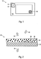
- Fig. 1 shows a schematic representation of a bank note 10, which is provided with two security elements 12 and 16 according to embodiments of the invention.
- the first security element represents a see-through security element 12, which is arranged over a see-through area 14, for example a window area or a continuous opening, of the bank note 10.
- the second security element 16 is formed by an opaque, glued-on transfer element of any shape.
- Both security elements have metallic nanostructures in a feature area in which incident visible light excites volume or surface plasmons or resonance effects that generate novel color effects that are difficult to forge due to the small size of the respective coloring nanostructures.
- plasmons represent the eigenmodes of collective vibrations of the free electrons relative to the ion cores in metals, which can be excited by incident electromagnetic radiation.
- the freely movable charge carriers are excited to resonant oscillations, so that the light of this wavelength is preferentially absorbed and scattered in all spatial directions.
- radiation with wavelengths outside the resonance range can pass largely undisturbed.
- the metallic nanostructures according to the invention appear in transparency with a color impression that results from the wavelengths of the unaffected, non-resonant portion of the incident light.
- the color impression of the nanostructures is mainly determined by the resonant portion of the spectrum. Which wavelengths can excite the resonant plasma oscillations depends not only on the material from which the nanostructures are made, but also on the shape and size of the nanostructures and the embedding medium.
- the embodiment not according to the invention of Fig. 2 shows first of all a see-through security element 20 with a substrate 22 and a feature area, which is formed by a feature layer applied over the entire surface 24 is formed.
- the feature layer 24 contains a multiplicity of metallic nanoparticles 28 which are embedded in a carrier medium 26.
- Such a feature layer 24 can be produced, for example, by printing on a transparent lacquer 26 in which prefabricated metallic nanoparticles 28 with desired properties are dissolved.
- the nanoparticles 28 have a diameter below the wavelength of visible light, preferably between 300 nm and 5 nm and in particular between 200 nm and 10 nm.
- the nanoparticles 28 are gold or silver particles.
- other metals such as copper, aluminum, nickel, chromium, tungsten, vanadium, palladium, platinum or alloys of these metals, albeit partially in a weakened or modified form, show color effects due to plasmon excitation, so that these metals or metal alloys are also considered to be Material for the nanoparticles 28 come into consideration.
- spherical nanoparticles 28 it is also possible to use particles of other shape, such as ellipsoids of revolution, any polyhedron or rod-shaped or platelet-shaped particles. Particles deviating from the spherical shape show, if they are oriented in a preferred direction in space, additional effects that are dependent on the polarization direction of the incident light.
- coated core-shell particles can also be used for color generation. These can have both a metallic core with a dielectric or metallic shell and a dielectric core with a metallic sheath. Examples of such designs are silver particles with a TiO 2 shell or polystyrene cores with a gold coating. There is hardly any limit to the number of possible combinations, especially since the materials can also be in crystalline or polycrystalline form in addition to the amorphous phase.
- the transparent lacquer 26, in which the nanoparticles 28 are dissolved is applied over the entire surface to the substrate 22, for example printed on, as in FIG Fig. 2 shown.
- Broadband incident light 30 then excites specific plasma oscillations (plasmons) in the nanoparticles 28 depending on the material, shape and size of the particles 28 and their embedding medium 26.
- plasma oscillations plasmas
- the resonance frequency for essentially spherical gold particles with a diameter of 50 nm is approximately 520 nm, for gold particles with a diameter of 150 nm it is approximately 580 nm.
- the nanoparticles 28 and the embedding medium 26 are matched to one another in such a way that the resonance frequency of the embedded nanoparticles 28 is green at a wavelength of approximately 530 nm.
- the feature layer 24 therefore appears green.
- the feature layer 24 appears in the subtractive complementary color, that is to say with a red color impression.
- the color impression of the metallic nanoparticles does not depend on the angle of incidence of the radiation and the viewing direction.
- the security elements according to the invention also do not run through the visible spectrum or sections thereof when tilted, but essentially have one constant color impression. Since the color effects are caused by nanostructures that are much smaller than the period of conventional diffraction gratings, they are particularly resistant to forgery, since such small structures can hardly be produced using conventional methods such as direct exposure or dot-matrix methods.
- the feature area of the security element 20 can also be designed in the form of patterns, characters or a code. It is also possible to provide different metallic nanostructures in different partial areas of the feature area, for example nanoparticles 28 made of different materials and / or nanoparticles 28 of different shapes and sizes. This allows different areas of the feature area to be colored differently.
- the lacquer 26 provided with the coloring nanoparticles 28 can additionally contain conventional color or effect pigments in order to modify the observable color effects.
- Different types of metallic nanoparticles 28, for example with varying diameters, can also be mixed with one another in order to produce a desired color effect in cooperation.
- measures can be taken to influence the spatial distribution of nanoparticles 28 initially homogeneously dispersed in a carrier medium or the preferred direction of non-spherical nanoparticles. This can be done, for example, by equipping the nanoparticles with a magnetic core so that they can be concentrated at the intended locations of the feature area with the aid of spatially varying magnetic fields.
- the nanoparticles 28 are initially still movable in the carrier medium 26.
- the binding agent of the carrier medium 26 is cured, for example by drying or irradiation with UV light, or the carrier medium 26 or at least the solvent contained therein is evaporated by supplying heat.
- Functionalized surfaces of nanoparticles offer additional possibilities to influence the arrangement of the nanoparticles. For example, through a suitable functionalization of the surface, it can be achieved that the particles are arranged at a certain distance and / or in a defined grid. In addition, a suitably selected functionalization can prevent clustering of the nanoparticles.
- Functionalization of the substrate surface can also serve to arrange and periodically align the nanoparticles.
- these can be deposited in a targeted manner on predefined areas of the substrate. This makes it possible, for example, to arrange the nanoparticles on grating lines in order to influence the diffraction property of the grating, for example to increase it.
- non-magnetic nanoparticles 28 can also be coupled to magnetic carrier particles by functional coatings, which are then specifically arranged and / or aligned together with the coloring nanoparticles 28 by external magnetic fields.
- the distribution of the nanoparticles 28 is specifically influenced by structuring the surface to which they are applied.
- a transparent UV-curing lacquer layer 40 can be provided with a desired relief embossing in a manner known per se, so that a structured surface with elevations 42 and depressions 44 is created.
- a fluid medium 46 in which the nanoparticles 48 are dissolved is then applied, for example printed, to the surface structured in this way. Then the fluid medium 46 is knife-coated or wiped off the coated surface, so that the nanoparticles 48 only remain in the depressions 44, but not on the raised surface regions 42.
- the structure can be covered with a further lacquer layer, not shown in the figures. If the lacquer used for covering flows around the nanoparticles 48, the refractive index of the medium embedding the particles can also be defined in this way. At present, however, it is preferred that the nanoparticles 48 remain embedded in the original carrier medium 46, which remains in the depressions 44 together with the nanoparticles 48 when the surface is doctored off.
- the in Fig. 4 is additionally provided with a metal layer 50 between substrate 22 and UV lacquer layer 40 in order to modify the color impression of the nanoparticles 48 in a targeted manner.
- a metal layer 52 is applied to the embossed UV lacquer layer 40, for example by vapor deposition, thereby modifying the color impression of the nanoparticles 48.
- microtogravure printing technology provides a mold, the surface of which has an arrangement of elevations and depressions in the form of a desired microstructure.
- the depressions of the tool mold are filled with a curable colored or colorless varnish containing the nanoparticles, and the carrier to be printed is pretreated for good anchoring of the varnish.
- the surface of the tool mold is then brought into contact with the carrier and the lacquer in contact with the carrier is hardened in the depressions of the tool mold and thereby bonded to the carrier.
- the visual impression can not only be generated by the effects of the plasmon excitation in the nanoparticles 48, but can also be influenced by diffraction effects on the structures that are predetermined by the elevations 42 and depressions 44.
- diffraction effects can be specifically integrated into the design of the security element. Are such in other designs Strongly color-producing additional effects are undesirable, so the elevations and depressions 42, 44 can also be arranged irregularly and color phenomena caused by diffraction can be largely suppressed.
- Fig. 6 (a) a plan view of the feature area 60 of a security element not according to the invention, in which the depressions 44 with the nanoparticles 48 are periodically arranged in two spatial directions.
- the period lengths denoted by px and py can be the same or different, so that the same or different diffraction color effects occur in the x-direction and y-direction.
- the depressions 44 with the nanoparticles 48 are only arranged periodically in the y-direction, while they are randomly distributed in the x-direction. Diffraction effects due to the periodic arrangement of the depressions 44 occur with such a design only in the y-direction, while they are suppressed in the x-direction. If the color-splitting diffraction effects are to be completely suppressed, the depressions 44 can also be arranged randomly in both spatial directions, as in the feature area 64 of FIG Fig. 6 (c) shown.
- Fig. 7 shows an embodiment 70 of a further variant not according to the invention, in which the nanoparticles 78 are integrated in a thin-film element 72 with a color-shift effect.
- a reflective metal layer 74 for example an aluminum layer with a thickness of at least 10 nm
- a dielectric intermediate layer 75 made of a UV-curable material and a semitransparent absorber layer 76, which can be formed, for example, by an approximately 8 nm thick chrome layer, is applied to a substrate 22 can.
- the intermediate dielectric layer 75 is preferably formed from a carrier medium with a high refractive index.
- the desired metallic nanoparticles 78 which can be achieved, for example, in that the nanoparticles 78 are admixed with the intermediate layer material before application.
- the filter effect of the nanoparticles 78 is combined with the color filter effect of the color-shifting thin-film system 72.
- the semitransparent absorber layer 76 can also be dispensed with. If the security element 70 is to be used in transmission, that is to say for example in the see-through window of a bank note, then the lower metal layer 74 is expediently designed to be semitransparent. It goes without saying that the feature area also in the exemplary embodiments of Figures 3 to 7 can be designed in the form of patterns, characters or a coding and that here too different metallic nanostructures can be provided in different partial areas. Both transparent and non-transparent layer systems can be used as the substrate 22.
- the substrate 22 can be formed, for example, by a transparent or opaque plastic film that remains in the finished security element or by a transfer film that is peeled off after the security element has been transferred to the bank note 10.
- the substrate 22 can also be formed by the bank note paper itself.
- the nanoparticles can, for example, be suspended in a primer before printing and printed directly onto the banknote paper.
- the production of the metallic nanoparticles themselves can take place by physical or chemical processes known to the person skilled in the art.
- a physical process is, for example, laser ablation.
- one or more subwavelength gratings can also be applied directly to the substrate of the security element according to the invention.
- Such periodic nanostructures allow stronger color effects than the previously described metallic nanoparticles, on the other hand the large number of degrees of freedom in the manufacture of counterfeit security of such security elements increases further.
- Wood anomalies also influence the transmission and reflection spectra of gratings in the zeroth diffraction order regardless of the polarization of the incident light.
- a Wood anomaly is associated with the creation of a new diffraction order, that is, it occurs when the angle of reflection is 90 °.
- FIG. 8 shows a cross section through a security element 80 with a transparent carrier film 82, on which a UV embossing lacquer layer 84 is printed and embossed in the form of a rectangular profile, which has a period length p, for example 300 nm, a web width b, for example 100 nm, and a pitch h , for example 100 nm.
- the metallic binary structure 86 embedded in the lacquer layers 84, 88 which contains exclusively flat metallic surface sections at only two different height levels (metallic bi-grating).
- the width of the metal application in the lower level is predetermined by the geometric shading during vapor deposition and that the thickness d of the metal film 90 is identical on the upper and lower levels.
- the transmission and reflection spectra of such subwavelength gratings can be calculated, for example, with the aid of electromagnetic diffraction theories.
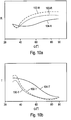
- the spectrum calculated for the visible wavelength range is convoluted with the spectrum of the standard lamp D65 and the sensitivity curves of the human eye. This results in the parameters X, Y and Z, which reflect the color values red, green and blue.
- Fig. 10 (a) the color values X (curve 100-R), Y (curve 102-R) and Z (curve 104-R) of the reflected light in the zeroth order of diffraction as a function of the vapor deposition angle Q are shown.
- Fig. 10 (b) shows the color values X (curve 100-T), Y (curve 102-T) and Z (curve 104-T) of the transmitted light also in the zeroth order of diffraction.
- a nano-structure becomes very colorful if one of the color values X, Y, Z is dominant compared to the other color values or if the color values differ greatly from one another.
- the color value Z dominates the transmission ( Fig. 10 (b) , Curve 104-T), while the color values X and Y dominate the reflected radiation ( Fig. 10 (a) , Curves 100-R, 102-R).
- Such subwavelength gratings thus appear with a clearly pronounced color in transmission and reflection.
- the reflection of an object is at least 20% so that the color spectrum reflected on the object stands out from the reflected light of the surrounding medium.
- the transmission can be lower for color perception, since usually only the transmitted light of the object is observed and the scattered light of the surroundings is covered.
- a reflection of 30% to 60% and a transmission between 5% and 45% are obtained for an evaporation angle Q in the range between 30 ° and 90 °. In the case of inclined vaporization angles, the transmission increases while the reflection is reduced.
- the color effect of the subwavelength gratings according to the invention changes when viewed in polarized light.
- the intensity of the color value Z blue
- the described subwavelength gratings can be combined with a diffraction structure which spectrally splits incident electromagnetic radiation.
- a security element 110 the feature area of which is provided with a metallized embossed structure 112 with two superimposed grids.
- the grating with the smaller grating period p s forms a sub-wavelength grating of the type described above.
- This sub-wavelength grating is superimposed with a second grating of a significantly larger period p 1 , which is used to generate a multiplication or spectral broadening of the resonances of the sub-wavelength grating described above.
- the plasmon resonances can be spectrally broadened.
- a broader range of the visible light spectrum can be influenced in its intensity than would be the case with a strictly periodic grating.
- FIG. 12 shows a schematic plan view of a feature area 120 with a rectangular cross grid 122 which is periodic in two spatial directions.
- the sequence of hatched and non-hatched rectangles 124, 126 each represents higher or lower lying metallized surface sections, as shown in cross section, for example in FIG Fig. 8 are shown.
- the cross grating 122 Due to the rectangular design of the cross grating 122, the period lengths in the x-direction and y-direction, px and py, are generally different. With different period lengths px, py, the cross grating 122 produces a different color impression in the polarized light, depending on whether the light is polarized vertically or horizontally. When viewing with unpolarized light, the viewer perceives a mixed color. If, on the other hand, the period lengths px and py are the same, the cross grating looks the same when viewed with unpolarized light as when viewed with vertically or horizontally polarized light.
- the one- or two-dimensional sub-wavelength gratings can also be formed by a repeated arrangement of metallic structural elements, In addition to square or rectangular elements, circular, elliptical, ring-shaped or any shaped elements can also be considered.
- Fig. 13 For illustration, in (a) shows a plan view 130 of a subwavelength grating which is formed from a two-dimensional periodic arrangement of ring elements 132.
- the ring width of the ring elements 132 is of particular importance.
- the strips 136 are excited by the external electromagnetic radiation. They transport the absorbed electromagnetic energy to the ring elements 132 and partially transfer it to them. Since structural elements of different geometry generally also have different plasmon resonances, such a combination of different structural elements can lead to a modified resonance behavior and thus to a changed color impression of the overall system.
- the arbitrarily shaped elements can be distributed statistically or stochastically on the surface that is to appear colored.
- the variants described for the one-dimensional subwavelength gratings in particular the use of Wood anomalies and the combination of the subwavelength gratings with diffraction gratings can also be used with two-dimensional cross gratings and the one- or two-dimensional structure element arrangements.
- the described subwavelength gratings can also be integrated into an interference layer system in order to modify or enhance their optical effect.
- An exemplary layer system is shown in the cross section of Fig. 14 shown.
- a UV embossing lacquer layer 142 is printed on a transparent carrier film 140 and embossed in the form of a desired one- or two-dimensional subwavelength grating.
- An aluminum layer 144 of a desired thickness is then vapor-deposited onto the embossing lacquer layer 142 perpendicularly or at a certain vapor deposition angle Q.
- the optical effect of the high-index dielectric layer 146 is essentially determined by its thickness and the difference in refractive index to the surroundings.
- the high resolution required for the described subwavelength gratings can be achieved, for example, with the aid of electron beam lithography systems, with even the smallest particles with a lateral extent of a few 10 nm still being produced with individual outlines can.
- PMMA is typically used as the resist.
- embossing tools with the help of which the nanostructures can then be reproduced by embossing in UV-curable lacquer or a thermoplastically deformable plastic on film webs.
- the metallic nanostructures are obtained in the next step by vapor deposition or sputtering with the appropriate material in the desired layer thickness, whereby it should be noted that the metal layer thickness should generally be smaller than the embossing depth.
- the metals used are preferably gold, silver, copper and aluminum.
- a particular advantage of the metallic nanostructures according to the invention is that they can be arranged in a sufficient number of periods or quasi-periods even in small microstructures with dimensions of a few micrometers.
- Typical examples of such microstructures are letters and symbols that form the micromotif images of a moiré magnification arrangement.
- the mode of operation and advantageous arrangements for such moiré magnification arrangements are given in the publications DE 10 2005 062 132 A1 and WO 2007/076952 A2 described, the disclosure content of which is included in the present application. If such microstructures are filled with nanostructures according to the invention, they can be given a color that is difficult or impossible to achieve in any other way, in particular with several colors in a very small space.
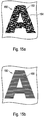
- Fig. 15 shows in (a) to (c) by way of example three embodiments of micromotif elements 150 which appear colored when filled with metallic nanostructures.
- the micromotif elements 150 shown in Fig. 15 for illustration are only represented by the letter "A", typically have a lateral dimension between 10 ⁇ m and 35 ⁇ m and a line width between 1 ⁇ m and 10 ⁇ m and can therefore be designed in color with conventional methods only with difficulty.
- the region of the micromotif elements 150 contains metallic nanoparticles 152 which are embedded in a carrier medium 154, as described in more detail above.
- the micromotif elements 150 of the Fig. 15 (b) are filled with a linear subwavelength grating 156, and the in Fig. 15 (c) micromotif elements 150 shown with a square cross grating 158.
- the color generation or blackening is brought about by the excitation of plasmons in the respective nanostructures 152, 156, 158, as already described above.
- the line grating 156 the period of which should be significantly smaller than the wavelength of visible light, a polarizing effect can also be observed in addition to the color effect.
- Which color is created in detail depends on the nature of the nanostructures and the type of dielectric embedding, as already explained in detail.
- the deterministic structures 156, 158 of the Figures 15 (b) and (c) can be produced by embossing in UV lacquer and subsequent vapor deposition of a metal layer of suitable thickness. If necessary, instead of a simple metal layer, a layer system can also be applied, as described above, for example in order to additionally intensify the plasmonic color effects.
- the surface sections provided with nanostructures can be located on the level of the vellum area or can be offset downwards or upwards in comparison to this level.
- Typical Embossing depths are in the range between 10 nm and 500 nm for the nanostructures and up to a maximum of 10 ⁇ m for the microstructures.
- the areas offset upwards or downwards, which define the surfaces of the micromotif elements 150 can also have curved profiles.
- the vellum area consists of an unstructured, smooth surface, while the surfaces forming the microstructures are equipped with nanostructures.
- the reverse case is also possible, in which the microstructures do not experience any additional structuring, but the surrounding vellum area is nanostructured.
- a combination of both possibilities comes into consideration, in which both the micromotif elements 160 and the surrounding vellum area 162 are provided with nanostructures 164, 166, each of which achieves different color effects.
- the nanostructures can also change within a microstructure, for example continuously, abruptly or statistically.
- the surface sections that do not contain any nanostructures can also be unstructured or filled with other structures.
- microstructures such as sawtooth structures or retroreflective cube-corner structures or so-called moth-eye structures that absorb light and therefore look dark to black are possible.
Description
Die Erfindung betrifft ein Sicherheitselement für Sicherheitspapiere, Wertdokumente und dergleichen mit einem Merkmalsbereich, der einfallende elektromagnetische Strahlung selektiv beeinflusst. Die Erfindung betrifft ferner ein Verfahren zur Herstellung eines derartigen Sicherheitselements sowie ein Sicherheitspapier und einen Datenträger mit einem solchen Sicherheitselement.The invention relates to a security element for security papers, documents of value and the like with a feature area which selectively influences incident electromagnetic radiation. The invention also relates to a method for producing such a security element as well as a security paper and a data carrier with such a security element.
Zur Echtheitsabsicherung von Kreditkarten, Banknoten und anderen Wertdokumenten werden seit einigen Jahren Hologramme, holographische Gitterbilder und andere hologrammähnliche Beugungsstrukturen eingesetzt. Metallisierte Prägehologramme, die vorzugsweise aus sinusförmigen Oberflächenprofilen mit Gitterperioden zwischen etwa 600 nm und 2 µm bestehen, dienen heutzutage auf unzähligen Banknoten als Zeichen ihrer Echtheit.For some years now, holograms, holographic grating images and other hologram-like diffraction structures have been used to ensure the authenticity of credit cards, bank notes and other documents of value. Metallized embossed holograms, which preferably consist of sinusoidal surface profiles with grating periods between approximately 600 nm and 2 μm, are used today on countless banknotes as a sign of their authenticity.
Um die Attraktivität und Fälschungssicherheit weiter zu steigern, wurde eine Vielzahl von optisch variablen Effekten entwickelt: Sobald die Banknote relativ zum Betrachter und/oder zur Lichtquelle bewegt wird, verändert das Hologramm sein Erscheinungsbild drastisch. Besonders typisch sind Farbänderungen, die sich in sogenannten Lauf-, Kipp- oder Morph-Effekten manifestieren. Diese optische Variabilität sowie der metallische Glanz der metallisierten Hologrammfolien sorgen dafür, dass sich echte Banknoten deutlich von Fälschungen unterscheiden, die mithilfe von Farbdruckern erstellt wurden. Vergleichbare optische Variabilität kann mit handelsüblichen Farben nicht erreicht werden. Beugungsgitter, die Grundbausteine derartiger Hologramme, erzeugen grundsätzlich eine spektrale Farbaufspaltung.In order to further increase the attractiveness and protection against forgery, a large number of optically variable effects have been developed: As soon as the bank note is moved relative to the viewer and / or the light source, the hologram changes its appearance drastically. Color changes that manifest themselves in so-called run, tilt or morph effects are particularly typical. This optical variability and the metallic sheen of the metallized hologram foils ensure that real banknotes are clearly different from counterfeits that were created with the help of color printers. Comparable optical variability cannot be achieved with commercially available colors. Diffraction gratings, the basic building blocks of such holograms, basically create a spectral color split.
Trotz des hohen Entwicklungsstandes, den die zum Schutz von Banknoten gegen Fälschung eingesetzten Hologramme mittlerweile erreicht haben, gelangen immer bessere Fälschungen auf den Markt. Die in den Hologrammen verwendeten Gitterperioden von mindestens 600 nm sind nicht nur mit Elektronenstrahllithographie-Anlagen, sondern auch durch interferometrische Direktbelichtung mithilfe eines Lasers herstellbar, wodurch die Fälschungssicherheit der Hologramme deutlich vermindert wird. Besonders häufig werden Hologrammfälschungen mithilfe von Dot-Matrix-Systemen angefertigt, deren Funktionsweise letztlich ebenfalls auf der Interferenz von Laserstrahlen beruht.Despite the high level of development that the holograms used to protect banknotes against counterfeiting have meanwhile reached, better and better counterfeits are coming onto the market. The grating periods of at least 600 nm used in the holograms can be produced not only with electron beam lithography systems, but also by interferometric direct exposure using a laser, which significantly reduces the forgery-proofness of the holograms. Falsified holograms are often produced with the help of dot matrix systems, the functionality of which is ultimately also based on the interference of laser beams.
Seit einiger Zeit werden auch sogenannte Moire-Vergrößerungsanordnungen als Sicherheitsmerkmale eingesetzt. Die prinzipielle Funktionsweise derartiger Moire-Vergrößerungsanordnungen ist in dem Artikel "
Aufgrund der geringen Strichstärke der in derartigen Moire-Vergrößerungsanordnungen eingesetzten Buchstaben und Symbole von etwa einem Mikrometer war es bisher nicht möglich, farbige Buchstaben durch fein strukturierte metallische Oberflächen zu erzeugen. Beugungseffekte kommen für die Farbgebung kaum infrage, weil Gitter mit den üblichen Perioden nicht oder nur in Spezialfällen in den Linien, aus denen die Buchstaben bzw. Symbole des Mikrostrukturarrays bestehen, untergebracht werden können. Darüber hinaus egalisiert das zur Betrachtung eingesetzten Linsenarray die Winkelaufspaltung einzelner Spektralfarben, so dass klassische Gitterbeugung in der ersten Beugungsordnung zur Farbgebung in Moire-Vergrößerungsanordnungen oder in den allgemeineren Modulo-Vergrößerungsanordnungen wenig geeignet ist.Due to the small line thickness of the letters and symbols used in such moiré magnification arrangements of approximately one micrometer, it has not previously been possible to produce colored letters through finely structured metallic surfaces. Diffraction effects are hardly an option for the coloring because lattices with the usual periods are not or only in special cases in the lines that make up the letters or symbols of the microstructure array. In addition, the lens array used for viewing equalizes the angular splitting of individual spectral colors, so that classic lattice diffraction in the first order of diffraction is not very suitable for coloring in moiré magnification arrangements or in the more general modulo magnification arrangements.
Die
Die
Davon ausgehend liegt der Erfindung die Aufgabe zugrunde, die Nachteile des Standes der Technik zu vermeiden und insbesondere ein Sicherheitselement mit einem attraktiven visuellen Erscheinungsbild und hoher Fälschungssicherheit zu schaffen.On this basis, the invention is based on the object of avoiding the disadvantages of the prior art and, in particular, of creating a security element with an attractive visual appearance and high level of protection against forgery.
Diese Aufgabe wird durch das Sicherheitselement mit den Merkmalen des Hauptanspruchs gelöst. Ein Verfahren zur Herstellung eines derartigen Sicherheitselements, ein Sicherheitspapier und ein Datenträger sind in den nebengeordneten Ansprüchen angegeben. Weiterbildungen der Erfindung sind Gegenstand der Unteransprüche.This object is achieved by the security element with the features of the main claim. A method for producing such a security element, a security paper and a data carrier are specified in the independent claims. Further developments of the invention are the subject of the subclaims.
Nach der Erfindung ist bei einem gattungsgemäßen Sicherheitselement vorgesehen, dass der Merkmalsbereich metallische Nanostrukturen enthält, in denen durch die einfallende elektromagnetische Strahlung Volumen- oder Oberflächenplasmonen angeregt und/oder Resonanzerscheinungen hervorgerufen werden.According to the invention, a generic security element provides that the feature area contains metallic nanostructures in which volume or surface plasmons are excited and / or resonance phenomena are caused by the incident electromagnetic radiation.
Plasmonen sind kollektive Schwingungen der freien Elektronen relativ zu den Ionenrümpfen in Metallen. Bei der sogenannten Plasmafrequenz tritt eine erhöhte Absorption des anregenden Lichtes auf. Durch Rekombination von Plasmonen in Strahlung kann Lichtstreuung auftreten, vor allem, wenn das Metall in Partikelform vorliegt. Oberflächenplasmon-Polaritonen (SPs) sind an metallische Grenzflächen gebundene elektromagnetische Strahlung, die sich entlang ihrer Grenzschicht ausbreitet und dabei eine Absorption erleidet. Die Anregung von Oberflächenplasmon-Polaritonen erfolgt über die Impulsanpassung des einfallenden Lichtes und den Oberflächenplasmon-Polaritonen über ein Dielektrikum bzw. über den reziproken Gittervektor der periodischen Strukturierung der Metalloberfläche.Plasmons are collective oscillations of free electrons relative to the ion cores in metals. At the so-called plasma frequency, there is an increased absorption of the stimulating light. By recombining plasmons in radiation, light scattering can occur, especially when the metal is in particulate form. Surface plasmon polaritons (SPs) are electromagnetic radiation bound to metallic interfaces, which propagates along their boundary layer and is absorbed in the process. The excitation of surface plasmon polaritons takes place via the pulse adaptation of the incident light and the surface plasmon polaritons via a dielectric or via the reciprocal lattice vector of the periodic structuring of the metal surface.
Ferner können an Subwellenlängengittern außergewöhnliche Intensitätsänderungen in der Transmission bzw. in der Reflexion auftreten, wenn das einfallende Licht zu Resonanzen in den Zwischenräumen bzw. in den Hohlräumen der Gitterstruktur führt. Auch derartige Resonanzeffekte können durch die Anregung von Oberflächenplasmonen bzw. Oberflächenpolaritonen durch die einfallende Strahlung erklärt werden. Man kann bei Transmissionsgittern hierbei eine starke Intensitätsumverteilung zwischen Reflexion und Transmission für bestimmte Wellenlängenbereiche beobachten. Diese sogenannten Hohlraumresonanzen führen ebenso zu einer erhöhten Absorption des Lichtes. Erwähnenswert ist, dass dieser Effekt auch eine außergewöhnliche Transmissionserhöhung hervorrufen kann.Furthermore, unusual intensity changes in the transmission or in the reflection can occur at subwavelength gratings if the incident light leads to resonances in the interstices or in the cavities of the grating structure. Such resonance effects can also be caused by the excitation of surface plasmons or surface polaritons can be explained by the incident radiation. In the case of transmission gratings, a strong redistribution of intensity between reflection and transmission can be observed for certain wavelength ranges. These so-called cavity resonances also lead to increased absorption of light. It is worth mentioning that this effect can also cause an extraordinary increase in transmission.
Auch wenn die genannten physikalischen Effekte gegenwärtig als die korrekte Beschreibung der auftretenden Phänomene angesehen werden, ist die vorliegende Erfindung durch die räumlich-körperliche Ausgestaltung der vorgeschlagenen Sicherheitselemente definiert und nicht an die gegebene Erklärung der Phänomene durch Anregung von Volumen- oder Oberflächenplasmonen oder dem Auftreten von Resonanzerscheinungen gebunden.Even if the mentioned physical effects are currently regarded as the correct description of the phenomena occurring, the present invention is defined by the spatial-physical configuration of the proposed security elements and not to the given explanation of the phenomena by excitation of volume or surface plasmons or the occurrence of Resonance phenomena bound.
Im Rahmen der Erfindung ist bevorzugt, wenn der Merkmalsbereich des Sicherheitselements einfallende elektromagnetische Strahlung im sichtbaren Spektralbereich selektiv beeinflusst. Insbesondere kann der Merkmalsbereich einfallende elektromagnetische Strahlung selektiv reflektieren und/oder transmittieren. Beispielsweise kann der Merkmalsbereich bestimmte Spektralanteile des sichtbaren Lichts reflektieren und andere Spektralanteile des sichtbaren Lichts transmittieren und so in Reflexion und Transmission mit unterschiedlichen Farben erscheinen.In the context of the invention, it is preferred if the feature range of the security element selectively influences incident electromagnetic radiation in the visible spectral range. In particular, the feature area can selectively reflect and / or transmit incident electromagnetic radiation. For example, the feature area can reflect certain spectral components of the visible light and transmit other spectral components of the visible light and thus appear with different colors in reflection and transmission.
Zur Ausbildung eines Durchsichtssicherheitselements kann der Merkmalsbereich insbesondere transparent oder transluzent ausgebildet sein. Bei Sicherheitselementen, die auf Betrachtung in Reflexion ausgelegt sind, kann der Merkmalsbereich oder das Substrat des Sicherheitselements auch opak sein.To form a see-through security element, the feature area can in particular be made transparent or translucent. In the case of security elements that are designed to be viewed in reflection, the feature area or the substrate of the security element can also be opaque.
Der Merkmalsbereich kann in verschiedenen Teilbereichen verschiedene metallische Nanostrukturen enthalten, beispielsweise um verschiedenfarbige Bereiche innerhalb des Sicherheitselements zu erzeugen.The feature area can contain different metallic nanostructures in different partial areas, for example in order to produce different colored areas within the security element.
Das Trägermedium ist im Rahmen der Erfindung vorzugsweise durch eine transparente oder gefärbte Lackschicht gebildet.In the context of the invention, the carrier medium is preferably formed by a transparent or colored lacquer layer.
Der Merkmalsbereich enthält als metallische Nanostrukturen ein oder mehrere Subwellenlängengitter mit Gitterperioden unterhalb der Wellenlänge des sichtbaren Lichts. Die Subwellenlängengitter sind als Binärstrukturen ausgebildet, die ausschließlich ebene metallische Flächenabschnitte auf nur zwei verschiedenen Höhenstufen enthalten.The feature area contains, as metallic nanostructures, one or more subwavelength gratings with grating periods below the wavelength of visible light. The subwavelength gratings are designed as binary structures that contain only flat metallic surface sections at only two different height levels.
Auch die Subwellenlängengitter können mit einer Beugungsstruktur kombiniert sein, die die einfallende elektromagnetische Strahlung spektral aufspaltet. Zur spektralen Verbreiterung der auftretenden Resonanzen können die Subwellenlängengitter Gitterlinien einer variierenden Breite aufweisen. Erfindungsgemäß werden durch Subwellenlängengitter, die eine laterale Variation der Gitterprofile, nämlich eine laterale Variation der Profiltiefen, aufweisen, lateral unterschiedliche Farbeindrücke erzeugt. In die Sicherheitselemente werden auf diese Weise beliebige farbige Bilder eingebracht, beispielsweise gerasterte Farbbilder, die aus einer Vielzahl kleiner und verschiedenfarbiger Pixelelemente bestehen.The subwavelength gratings can also be combined with a diffraction structure that spectrally splits the incident electromagnetic radiation. For the spectral broadening of the resonances that occur, the subwavelength gratings can have grating lines of varying width. According to the invention, laterally different color impressions are generated by subwavelength gratings which have a lateral variation of the grating profiles, namely a lateral variation of the profile depths. In this way, any color images are introduced into the security elements, for example screened color images which consist of a large number of small and differently colored pixel elements.
Erfindungsgemäß enthält das Sicherheitselement ein farbiges Bild aus einer Mehrzahl von Pixelelementen, wobei die Gitterprofile innerhalb eines Pixelelements jeweils konstant sind und bei dem die Gitterprofile verschiedenfarbiger Pixelelemente entsprechend dem jeweils gewünschten Farbeindruck unterschiedlich ausgebildet sind.According to the invention, the security element contains a colored image made up of a plurality of pixel elements, the grid profiles within a pixel element being constant and in which the grid profiles are of different colors Pixel elements are designed differently in accordance with the respective desired color impression.
Die Farbbilderzeugung durch Subwellenlängengitter eignet sich insbesondere für schräg metallisch bedampfte dielektrische Gitter, die in Transmission und Reflexion unterschiedliche Farben zeigen, wie weiter unten genauer erläutert. Aufgrund des asymmetrischen Gitterprofils ist dabei in der Regel auch eine Asymmetrie der Farberscheinung im Betrachtungswinkel in Transmission bzw. in Reflexion zu beobachten. Die laterale Variation des Gitterprofils kann insbesondere in einer lateralen Variation der Grabentiefe des metallisierten dielektrischen Gitters bestehen. Neben Binärstrukturen kommen auch schräg bedampfte asymmetrische Multilevelprofile mit lateral unterschiedlichen Tiefen in Betracht.The generation of color images by means of subwavelength gratings is particularly suitable for diagonally metallically vapor-deposited dielectric gratings which show different colors in transmission and reflection, as explained in more detail below. Due to the asymmetrical grating profile, an asymmetry of the color appearance in the viewing angle in transmission or in reflection can usually be observed. The lateral variation of the grating profile can in particular consist of a lateral variation of the trench depth of the metallized dielectric grating. In addition to binary structures, obliquely vaporized asymmetrical multilevel profiles with laterally different depths can also be considered.
Um Subwellenlängengitter mit unterschiedlicher Profiltiefe zu erzeugen, kann beispielsweise wie folgt vorgegangen werden: Zunächst wird auf ein Gittersubstrat mit lateral konstanter Grabentiefe Photolack aufgebracht, so dass die Gräben komplett gefüllt sind. Dann wird das Substrat mit dem aufgebrachten Photolack mit Laserstrahlung lateral unterschiedlicher Intensität beaufschlagt und die Gräben durch Entfernen des belichteten Photolacks teilweise freigelegt.In order to generate subwavelength gratings with different profile depths, the following procedure can be used, for example: First, photoresist is applied to a grating substrate with a laterally constant trench depth, so that the trenches are completely filled. The substrate with the applied photoresist is then exposed to laser radiation of different intensity laterally and the trenches are partially exposed by removing the exposed photoresist.
Für die Farberzeugung kommt als zugrunde liegender physikalischer Effekt insbesondere die Polarisationskonversion durch Resonanzanregung an Gittern infrage, die zu einer selektive Transmission bzw. Reflexion bei Anordnung eines Subwellenlängengitters zwischen zwei gekreuzten Polarisatoren führt.The underlying physical effect for color generation is in particular polarization conversion through resonance excitation on gratings, which leads to selective transmission or reflection when a subwavelength grating is arranged between two crossed polarizers.
Die Gitterperioden der Subwellenlängengitter liegen vorzugsweise zwischen 10 nm und 500 nm, bevorzugt zwischen 50 nm und 400 nm und besonders bevorzugt zwischen 100 nm und 350 nm.The grating periods of the subwavelength gratings are preferably between 10 nm and 500 nm, preferably between 50 nm and 400 nm and particularly preferably between 100 nm and 350 nm.
Die Subwellenlängengitter können durch lineare, eindimensionale Gitter gebildet sein oder auch durch zweidimensionale Kreuzgitter, die in einer oder zwei Raumrichtungen periodisch sind. In einer weiteren Variante sind die Subwellenlängengitter durch ein- oder zweidimensionale wiederholte Anordnung von metallischen Strukturelementen gebildet, wobei die Strukturelemente insbesondere in Form von Quadraten, Rechtecken, Kreisflächen, Ringstrukturen, Streifen oder einer Kombination dieser Elemente oder eine beliebige andere Form gebildet sind. Als weitere Formen kommen insbesondere Kugeln, Rhomben oder Stäbchen, aber auch stark asymmetrische Formen, wie etwa offene Ringe, in Betracht. Alle genannten Anordnungen können in einer oder zwei Raumrichtungen periodisch sein.The subwavelength gratings can be formed by linear, one-dimensional gratings or also by two-dimensional cross gratings which are periodic in one or two spatial directions. In a further variant, the subwavelength gratings are formed by one or two-dimensional repeated arrangement of metallic structural elements, the structural elements being in particular in the form of squares, rectangles, circular areas, ring structures, strips or a combination of these elements or any other shape. Other possible shapes are, in particular, spheres, rhombuses or rods, but also strongly asymmetrical shapes such as open rings. All the arrangements mentioned can be periodic in one or two spatial directions.
Neben ein- oder zweidimensionalen linearen Gittern können erfindungsgemäß auch ein- oder zweidimensionale gekrümmte Gitter vorgesehen sein. Bei diesen gekrümmten Gittern verändert sich der Azimutwinkel der Gitterlinien ohne abrupte Sprünge kontinuierlich. Der Azimutwinkel gibt dabei den lokalen Winkel zwischen den Gitterlinien (genauer einer Tangente an die Gitterlinien) und einer Referenzrichtung an, beschreibt also die lokale Orientierung der Gitterlinien in der Ebene.In addition to one- or two-dimensional linear grids, one- or two-dimensional curved grids can also be provided according to the invention. With these curved grids, the azimuth angle of the grid lines changes continuously without abrupt jumps. The azimuth angle indicates the local angle between the grid lines (more precisely a tangent to the grid lines) and a reference direction, i.e. it describes the local orientation of the grid lines in the plane.
Die Subwellenlängengitter können in ein Interferenzschichtsystem integriert sein, um ihre optische Wirkung zu modifizieren oder zu verstärken.The subwavelength gratings can be integrated into an interference layer system in order to modify or enhance their optical effect.
In allen Erfindungsvarianten kann der Merkmalsbereich in Form von Mustern, Zeichen oder einer Codierung vorliegen.In all variants of the invention, the feature area can be in the form of patterns, characters or a code.
Aufgrund der Kleinheit der metallischen Nanostrukturen können diese mit besonderem Vorteil in Sicherheitselementen eingesetzt werden, deren Merkmalsbereiche Mikrostrukturen mit einer Strichstärke zwischen etwa 1 µm und etwa 10 µm enthalten. Beispiele derartiger Sicherheitselemente stellen mikrooptische Moire-Vergrößerungsanordnungen dar, wie sie in den Druckschriften
In einer vorteilhaften Weiterbildung der Erfindung bilden die Mikrostrukturen dazu ein Motivbild, das in eine Mehrzahl von Zellen eingeteilt ist, in denen jeweils abgebildete Bereiche eines vorgegebenen Sollbilds angeordnet sind. Die lateralen Abmessungen der abgebildeten Bereiche liegen vorzugsweise zwischen etwa 5 µm und etwa 50 µm, insbesondere zwischen etwa 10 µm und etwa 35 µm. Bei den oben zuerst genannten mikrooptischen Moire-Vergrößerungsanordnungen stellen die abgebildeten Bereiche der Zellen des Motivbilds jeweils verkleinerte Abbilder des vorgegebenen Sollbilds dar, die vollständig innerhalb einer Zelle Platz finden. Bei den mikrooptischen Vergrößerungsanordnungen vom Moiretyp stellen die abgebildeten Bereiche mehrerer beabstandeter Zellen des Motivbilds zusammengenommen jeweils ein verkleinertes Abbild des Sollbilds dar, dessen Ausdehnung größer als eine Zelle des Motivbilds ist. Im allgemeinsten Fall stellt die Vergrößerungsanordnung eine Modulo-Vergrößerungsanordnung dar, bei der die abgebildeten Bereiche der Zellen des Motivbilds jeweils durch eine Modulo-Operation abgebildete, nicht vollständige Ausschnitte des vorgegebenen Sollbilds darstellen.In an advantageous development of the invention, the microstructures for this purpose form a motif image which is divided into a plurality of cells in which each of the mapped areas of a predetermined target image are arranged. The lateral dimensions of the areas shown are preferably between approximately 5 μm and approximately 50 μm, in particular between approximately 10 μm and approximately 35 μm. In the case of the above-mentioned first-mentioned micro-optical moiré magnification arrangements, the depicted areas of the cells of the motif image each represent reduced images of the predefined target image which are completely accommodated within a cell. In the case of the micro-optical magnification arrangements of the moiré type, the depicted Areas of several spaced apart cells of the motif image taken together each represent a reduced image of the target image, the extent of which is larger than a cell of the motif image. In the most general case, the magnification arrangement represents a modulo magnification arrangement in which the mapped areas of the cells of the motif image each represent incomplete sections of the specified target image mapped by a modulo operation.
Das Sicherheitselement weist vorzugsweise weiter ein Betrachtungsraster aus einer Mehrzahl von Betrachtungsrasterelementen zur Rekonstruktion des vorgegebenen Sollbilds bei der Betrachtung des Motivbilds mithilfe des Betrachtungsrasters auf. Die lateralen Abmessungen der Betrachtungsrasterelemente liegen dabei mit Vorteil zwischen etwa 5 µm und etwa 50 µm, insbesondere zwischen etwa 10 µm und etwa 35 µm.The security element preferably also has a viewing grid made up of a plurality of viewing grid elements for reconstructing the predetermined target image when viewing the motif image with the aid of the viewing grid. The lateral dimensions of the viewing grid elements are advantageously between approximately 5 μm and approximately 50 μm, in particular between approximately 10 μm and approximately 35 μm.
Im Spezialfall einer mikrooptischen Moire-Vergrößerungsanordnung wird als Mikrostruktur vorzugsweise ein Motivbild aus einer planaren periodischen oder zumindest lokal periodischen Anordnung einer Mehrzahl von Mikromotivelementen aufgebracht. Die lateralen Abmessungen der Mikromotivelemente liegen dabei mit Vorteil zwischen etwa 5 µm und etwa 50 µm, vorzugsweise zwischen etwa 10 µm und etwa 35 µm. Zusätzlich wird die gegenüberliegende Seite des Trägers zweckmäßig mit einer planaren periodischen oder zumindest lokal periodischen Anordnung einer Mehrzahl von Mikrofokussierelementen zur Moire-vergrößerten Betrachtung der Mikromotivelemente des Motivbilds versehen. In manchen Ausgestaltungen bietet es sich an, die Mikrofokussierelemente und die Mikromotivelemente auf derselben Seite des Trägers anzuordnen. Auch beidseitige Gestaltungen, bei denen eine Mikromotivelement-Anordnung durch zwei gegenüberliegende Mikrofokussierelement-Anordnungen betrachtet werden kann, kommen infage.In the special case of a micro-optical moiré magnification arrangement, a motif image from a planar periodic or at least locally periodic arrangement of a plurality of micromotif elements is preferably applied as the microstructure. The lateral dimensions of the micromotif elements are advantageously between approximately 5 μm and approximately 50 μm, preferably between approximately 10 μm and approximately 35 μm. In addition, the opposite side of the carrier is expediently provided with a planar periodic or at least locally periodic arrangement of a plurality of microfocusing elements for the moiré-enlarged observation of the micromotif elements of the motif image. In some configurations it is advisable to arrange the microfocusing elements and the micromotif elements on the same side of the carrier. Also bilateral designs in which a micromotif element arrangement is replaced by two opposite Microfocusing element arrays can be considered infage.
Die Erfindung enthält auch ein Verfahren zum Herstellen eines Sicherheitselements der beschriebenen Art.The invention also includes a method for producing a security element of the type described.
Dabei werden als metallische Nanostrukturen ein oder mehrere Subwellenlängengitter mit Gitterperioden unterhalb der Wellenlänge des sichtbaren Lichts auf ein Substrat aufgebracht. Dazu kann beispielsweise in eine Prägelackschicht eine Reliefstruktur in Form der gewünschten Subwellenlängengitter eingeprägt werden und auf diese Reliefstruktur eine Metallisierung aufgebracht, insbesondere aufgedampft werden. Die Metallisierung wird zweckmäßig in einem Aufdampfwinkel Q aufgedampft, der zwischen 0° und 90°, vorzugsweise zwischen 30° und 80° liegt. Die metallisierte Reliefstruktur wird dann vorteilhaft mit einer weiteren Lackschicht abgedeckt.One or more subwavelength gratings with grating periods below the wavelength of visible light are applied to a substrate as metallic nanostructures. For this purpose, for example, a relief structure in the form of the desired subwavelength gratings can be embossed into an embossed lacquer layer and a metallization can be applied, in particular vapor-deposited, to this relief structure. The metallization is expediently vapor deposited at a vapor deposition angle Q which is between 0 ° and 90 °, preferably between 30 ° and 80 °. The metallized relief structure is then advantageously covered with a further lacquer layer.
Als Subwellenlängengitter kann auch eine ein- oder zweidimensionale wiederholte Anordnung von metallischen Strukturelementen auf das Substrat aufgebracht, insbesondere aufgedampft werden, wie weiter unten genauer beschrieben.A one- or two-dimensional repeated arrangement of metallic structural elements can also be applied to the substrate, in particular vapor-deposited, as a sub-wavelength grating, as described in more detail below.
In einem weiteren vorteilhaften Herstellungsverfahren werden die Nanostrukturen durch Laserbestrahlung einer dünnen Metallschicht erzeugt. Die Metallschicht kann dabei auf strukturierten oder unstrukturierten Bereichen eines Substrats angeordnet sein und entweder frei liegen oder eingebettet sein. Die Metallschicht kann sowohl vollflächig sein und mit einem Laser vollflächig beschossen werden, als auch nur bereichsweise ausgebildet sein, so dass die Laserbestrahlung nur in den metallisierten und beleuchteten Bereichen zur Ausbildung von Nanostrukturen führt. In einer weiteren Ausgestaltung kann eine vollflächige Metallschicht nur an vorbestimmten Stellen mit Laserstrahlung, beispielsweise der Strahlung eines fokussierten Lasers, senkrecht oder schräg beleuchtet werden, so dass Nanostrukturen nur an den beleuchteten Stellen entstehen.In a further advantageous production method, the nanostructures are produced by laser irradiation of a thin metal layer. The metal layer can be arranged on structured or unstructured areas of a substrate and either be exposed or embedded. The metal layer can be full-area and bombarded with a laser over the full area, or it can only be formed in certain areas, so that the laser irradiation leads to the formation of nanostructures only in the metallized and illuminated areas. In a further embodiment For example, a full-surface metal layer can only be illuminated vertically or at an angle at predetermined points with laser radiation, for example the radiation of a focused laser, so that nanostructures only arise at the illuminated points.
Die Erfindung enthält ferner ein Sicherheitspapier für die Herstellung von Wertdokumenten oder dergleichen sowie einen Datenträger, insbesondere ein Wertdokument, wie eine Banknote, ein Pass, eine Urkunde, eine Ausweiskarte oder dergleichen. Das Sicherheitspapier bzw. der Datenträger sind erfindungsgemäß mit einem Sicherheitselement der beschriebenen Art ausgestattet. Das Sicherheitselement kann, insbesondere wenn es auf einem transparenten oder transluzenten Substrat vorliegt, auch in oder über einem Fensterbereich oder einer durchgehenden Öffnung des Sicherheitspapiers bzw. des Datenträgers angeordnet sein.The invention also contains a security paper for the production of documents of value or the like as well as a data carrier, in particular a document of value such as a bank note, a passport, a certificate, an identity card or the like. According to the invention, the security paper or the data carrier is equipped with a security element of the type described. The security element can, in particular when it is present on a transparent or translucent substrate, also be arranged in or above a window area or a continuous opening in the security paper or the data carrier.
Weitere Ausführungsbeispiele sowie Vorteile der Erfindung werden nachfolgend anhand der Figuren erläutert. Zur besseren Anschaulichkeit wird in den Figuren auf eine maßstabs- und proportionsgetreue Darstellung verzichtet.Further exemplary embodiments and advantages of the invention are explained below with reference to the figures. For the sake of clarity, a representation true to scale and proportion is dispensed with in the figures.
Die in den
Es zeigen:
- Fig. 1
- eine schematische Darstellung einer Banknote mit einem Durchsichtssicherheitselement und einem aufgeklebten Transferelement, jeweils nach Ausführungsbeispielen der Erfindung,
- Fig. 2
- ein nicht erfindungsgemäßes Durchsichtssicherheitselement im Querschnitt,
- Fig. 3 bis 5
- nicht erfindungsgemäße Ausführungsbeispiele mit strukturierten Oberflächen zur Steuerung der räumlichen Verteilung der metallischen Nanopartikel,
- Fig. 6
- in (a) bis (c) Aufsichten auf Merkmalsbereiche weiterer Sicherheitselemente,
- Fig. 7
- ein nicht erfindungsgemäßes Ausführungsbeispiel, bei dem metallische Nanopartikel in ein Dünnschichtelement mit Farbkippeffekt integriert sind,
- Fig. 8 und 9
- schematische Querschnitte durch ein erfindungsgemäßes Sicherheitselement gemäß der
Figur 8 mit Subwellenlängengitter und durch ein nicht erfindungsgemäßes Sicherheitselement gemäß derFigur 9 mit Subwellenlängengitter, - Fig. 10
- stark schematisiert die Farbigkeit bestimmter, erfindungsgemäßer Subwellenlängengitter in Abhängigkeit von dem Bedampfungswinkel Q, wobei in (a) die Farbigkeit in Reflexion und in (b) die Farbigkeit in Transmission, jeweils in der nullten Beugungsordnung gezeigt ist,
- Fig. 11
- ein erfindungsgemäßes Sicherheitselement, dessen Merkmalsbereich mit einer metallisierten Prägestruktur mit zwei überlagerten Gittern versehen ist,
- Fig. 12
- eine schematische Aufsicht auf einen Merkmalsbereich mit einem in zwei Raumrichtungen periodischen, rechteckigen Kreuzgitter,
- Fig. 13
- in (a) und (b) Aufsichten auf Subwellenlängengitter, die aus zweidimensionalen periodischen Anordnungen von Strukturelementen gebildet sind,
- Fig. 14
- ein in ein Interferenzschichtsystem integriertes Subwellenlängengitter,
- Fig. 15
- in (a) bis (c) drei Ausführungsformen von Mikromotivelementen, die durch Füllung mit metallischen Nanostrukturen farbig erscheinen, und
- Fig. 16
- ein Ausführungsbeispiel wie in
Fig. 15 , bei dem sowohl die Mikromotivelemente als auch der umgebende Velinbereich nanostrukturiert sind.
- Fig. 1
- a schematic representation of a banknote with a see-through security element and a glued-on transfer element, each according to exemplary embodiments of the invention,
- Fig. 2
- a see-through security element not according to the invention in cross section,
- Figures 3 to 5
- Embodiments not according to the invention with structured surfaces for controlling the spatial distribution of the metallic nanoparticles,
- Fig. 6
- in (a) to (c) supervision of feature areas of further security elements,
- Fig. 7
- an exemplary embodiment not according to the invention in which metallic nanoparticles are integrated into a thin-film element with a color-shift effect,
- Figures 8 and 9
- schematic cross-sections through a security element according to the invention according to FIG
Figure 8 with a subwavelength grating and by a security element not according to the invention according to FIGFigure 9 with subwavelength grating, - Fig. 10
- The color of certain subwavelength gratings according to the invention is strongly schematized as a function of the vapor deposition angle Q, whereby in (a) the color in reflection and in (b) the color in transmission, in each case in the zeroth order of diffraction,
- Fig. 11
- a security element according to the invention, the feature area of which is provided with a metallized embossed structure with two superimposed grids,
- Fig. 12
- a schematic plan view of a feature area with a rectangular cross grating that is periodic in two spatial directions,
- Fig. 13
- in (a) and (b) plan views of subwavelength gratings, which are formed from two-dimensional periodic arrangements of structural elements,
- Fig. 14
- a sub-wavelength grating integrated into an interference layer system,
- Fig. 15
- in (a) to (c) three embodiments of micromotif elements that appear colored when filled with metallic nanostructures, and
- Fig. 16
- an embodiment as in
Fig. 15 , in which both the micromotif elements and the surrounding vellum area are nano-structured.
Die Erfindung wird nun am Beispiel von Sicherheitselementen für Banknoten erläutert.
Beide Sicherheitselemente weisen in einem Merkmalsbereich metallische Nanostrukturen auf, in denen durch einfallendes sichtbares Licht Volumen- oder Oberflächenplasmonen angeregt bzw. Resonanzeffekte hervorgerufen werden, die neuartige Farbeffekte erzeugen, die aufgrund der Kleinheit der jeweils farbgebenden Nanostrukturen nur schwer zu fälschen sind.Both security elements have metallic nanostructures in a feature area in which incident visible light excites volume or surface plasmons or resonance effects that generate novel color effects that are difficult to forge due to the small size of the respective coloring nanostructures.
Wie oben bereits erläutert, stellen Plasmonen die Eigenmoden kollektiver Schwingungen der freien Elektronen relativ zu den Ionenrümpfen in Metallen dar, die durch einfallende elektromagnetische Strahlung angeregt werden können. Bei einer bestimmten Wellenlänge werden die frei beweglichen Ladungsträger zu resonanten Schwingungen anregt, so dass das Licht dieser Wellenlänge bevorzugt absorbiert und in alle Raumrichtungen gestreut wird. Strahlung mit Wellenlängen außerhalb des Resonanzbereichs kann dagegen weitgehend ungestört passieren.As already explained above, plasmons represent the eigenmodes of collective vibrations of the free electrons relative to the ion cores in metals, which can be excited by incident electromagnetic radiation. At a certain wavelength, the freely movable charge carriers are excited to resonant oscillations, so that the light of this wavelength is preferentially absorbed and scattered in all spatial directions. In contrast, radiation with wavelengths outside the resonance range can pass largely undisturbed.
Durch diesen Effekt erscheinen die erfindungsgemäßen metallischen Nanostrukturen in Durchsicht mit einem Farbeindruck, der sich aus den Wellenlängen des unbeeinflussten, nichtresonanten Anteils des einfallenden Lichts ergibt. Bei Betrachtung in Reflexion, bei der das Streulicht das visuelle Erscheinungsbild dominiert, wird der Farbeindruck der Nanostrukturen dagegen hauptsächlich durch den resonanten Anteil des Spektrums bestimmt. Welche Wellenlängen die resonanten Plasmaschwingungen anregen können, hängt neben dem Material, aus dem die Nanostrukturen bestehen, auch von der Form und Größe der Nanostrukturen und dem einbettenden Medium ab.As a result of this effect, the metallic nanostructures according to the invention appear in transparency with a color impression that results from the wavelengths of the unaffected, non-resonant portion of the incident light. When viewed in reflection, in which the scattered light dominates the visual appearance, the color impression of the nanostructures, on the other hand, is mainly determined by the resonant portion of the spectrum. Which wavelengths can excite the resonant plasma oscillations depends not only on the material from which the nanostructures are made, but also on the shape and size of the nanostructures and the embedding medium.
Das nicht erfindungsgemäße Ausführungsbeispiel der
Die Nanopartikel 28 weisen einen Durchmesser unterhalb der Wellenlänge des sichtbaren Lichts, vorzugsweise zwischen 300 nm und 5 nm und insbesondere zwischen 200 nm und 10 nm auf. In einer bevorzugten Erfindungsvariante handelt es sich bei den Nanopartikeln 28 um Gold- oder Silber-Partikel. Allerdings zeigen auch andere Metalle, wie etwa Kupfer, Aluminium, Nickel, Chrom, Wolfram, Vanadium, Palladium, Platin oder Legierungen dieser Metalle, wenn auch teilweise in abgeschwächter oder modifizierter Form, Farbeffekte aufgrund von Plasmonenanregung, so dass auch diese Metalle oder Metalllegierungen als Material für die Nanopartikel 28 in Betracht kommen.The
Neben kugelförmigen Nanopartikeln 28 können auch anders geformte Partikel, wie etwa Rotationsellipsoide, beliebige Vielflächler oder auch stäbchen-oder plättchenförmige Partikel eingesetzt werden. Von der Kugelform abweichende Partikel zeigen, wenn sie nach einer Vorzugsrichtung im Raum orientiert sind, zusätzlich von der Polarisationsrichtung des einfallenden Lichts abhängige Effekte.In addition to
Neben homogenen metallischen Nanopartikeln 28 kommen auch beschichtete Kern-Hülle Teilchen für die Farberzeugung in Betracht. Diese können sowohl einen metallischen Kern mit dielektrischer oder metallischer Hülle aufweisen als auch einen dielektrischen Kern mit metallischer Ummantelung. Beispiele für derartige Gestaltungen sind Silber-Partikel mit einer TiO2-Hülle oder Polystyrol-Kerne mit einer Gold-Beschichtung. Der Zahl an Kombinationsmöglichkeiten ist hier kaum eine Grenze gesetzt, zumal die Materialien neben der amorphen Phase auch in kristalliner bzw. polykristalliner Form vorliegen können.In addition to homogeneous
Im einfachsten Fall wird der transparente Lack 26, in dem die Nanopartikel 28 gelöst sind, vollflächig auf das Substrat 22 aufgetragen, beispielsweise aufgedruckt, wie in
Im Ausführungsbeispiel der
Anders als bei periodischen Beugungsstrukturen oder Interferenzschichtsystemen hängt der Farbeindruck der metallischen Nanopartikel nicht vom Einfallswinkel der Strahlung und der Betrachtungsrichtung ab. Die erfindungsgemäßen Sicherheitselemente durchlaufen beim Kippen auch nicht das sichtbare Spektrum oder Ausschnitte davon, sondern weisen einen im Wesentlichen konstanten Farbeindruck auf. Da die Farbeffekte durch Nanostrukturen, die wesentlich kleiner als die Periode herkömmlicher Beugungsgitter sind, hervorgerufen werden, weisen sie eine besonders hohe Fälschungssicherheit auf, da derart kleine Strukturen mit herkömmlichen Verfahren, wie etwa Direktbelichtung oder Dot-Matrix-Verfahren, kaum herzustellen sind.In contrast to periodic diffraction structures or interference layer systems, the color impression of the metallic nanoparticles does not depend on the angle of incidence of the radiation and the viewing direction. The security elements according to the invention also do not run through the visible spectrum or sections thereof when tilted, but essentially have one constant color impression. Since the color effects are caused by nanostructures that are much smaller than the period of conventional diffraction gratings, they are particularly resistant to forgery, since such small structures can hardly be produced using conventional methods such as direct exposure or dot-matrix methods.
Anstatt vollflächig ausgebildet zu sein, kann der Merkmalsbereich des Sicherheitselements 20 auch in Form von Mustern, Zeichen oder einer Codierung gestaltet sein. Es ist auch möglich, in verschiedenen Teilbereichen des Merkmalsbereichs verschiedene metallische Nanostrukturen vorzusehen, beispielsweise Nanopartikel 28 aus unterschiedlichen Materialien und/oder Nanopartikel 28 verschiedener Form und Größe. Dadurch können verschiedene Bereiche des Merkmalsbereichs unterschiedlich eingefärbt werden.Instead of being designed over the full area, the feature area of the
Darüber hinaus kann der mit den farbgebenden Nanopartikeln 28 versehene Lack 26 zusätzlich herkömmliche Farb- oder Effektpigmente enthalten, um die beobachtbaren Farbeffekte zu modifizieren. Auch können verschiedene Arten von metallischen Nanopartikeln 28, beispielsweise mit variierendem Durchmesser, miteinander vermischt werden, um in Zusammenwirkung eine gewünschte Farbwirkung zu erzeugen.
In einer weiteren Ausgestaltung können Maßnahmen ergriffen werden, um die räumliche Verteilung von zunächst homogen in einem Trägermedium dispergierten Nanopartikeln 28 oder die Vorzugsrichtung nicht-sphärischer Nanopartikel zu beeinflussen. Dies kann beispielsweise dadurch geschehen, dass die Nanopartikel mit einem magnetischen Kern ausgestattet werden, so dass sie mithilfe räumlich variierender Magnetfelder an den vorgesehenen Orten des Merkmalsbereichs konzentriert werden können. Die Nanopartikel 28 sind dabei zunächst noch im Trägermedium 26 beweglich. Erst nachdem sie mithilfe des Magnetfelds platziert und/oder ausgerichtet wurden, werden sie immobilisiert, indem das Bindemittel des Trägermediums 26, beispielsweise durch Trocknen oder Bestrahlung mit UV-Licht ausgehärtet wird, oder das Trägermedium 26 oder zumindest das darin enthaltene Lösungsmittel durch Wärmezufuhr verdampft wird.In addition, the
In a further embodiment, measures can be taken to influence the spatial distribution of
Funktionalisierte Oberflächen von Nanopartikeln bieten zusätzliche Möglichkeiten, die Anordnung der Nanopartikel zu beeinflussen. Beispielsweise kann durch eine geeignete Funktionalisierung der Oberfläche erreicht werden, dass sich die Partikel in einem bestimmten Abstand und/oder in einem definierten Gitter anordnen. Darüber hinaus kann durch eine geeignet gewählte Funktionalisierung eine Clusterbildung der Nanopartikel verhindert werden.Functionalized surfaces of nanoparticles offer additional possibilities to influence the arrangement of the nanoparticles. For example, through a suitable functionalization of the surface, it can be achieved that the particles are arranged at a certain distance and / or in a defined grid. In addition, a suitably selected functionalization can prevent clustering of the nanoparticles.
Auch eine Funktionalisierung der Substratoberfläche kann der Anordnung und periodischen Ausrichtung der Nanopartikel dienen. Durch eine Funktionalisierung der Substratoberfläche und gegebenenfalls auch der Oberfläche der Nanopartikel können diese gezielt auf vordefinierten Bereichen des Substrats deponiert werden. Dadurch ist es beispielsweise möglich, die Nanopartikel auf Gitterlinien anzuordnen, um die Beugungseigenschaft des Gitters zu beeinflussen, beispielsweise zu verstärken.
Alternativ können auch an sich unmagnetische Nanopartikel 28 durch funktionale Beschichtungen an magnetische Träger-Partikel gekoppelt werden, die dann zusammen mit den farbgebenden Nanopartikeln 28 durch externe Magnetfelder gezielt angeordnet und/oder ausgerichtet werden.Functionalization of the substrate surface can also serve to arrange and periodically align the nanoparticles. By functionalizing the substrate surface and possibly also the surface of the nanoparticles, these can be deposited in a targeted manner on predefined areas of the substrate. This makes it possible, for example, to arrange the nanoparticles on grating lines in order to influence the diffraction property of the grating, for example to increase it.
Alternatively,
Nach einer bevorzugten Erfindungsvariante wird die Verteilung der Nanopartikel 28 durch eine Strukturierung der Oberfläche, auf die sie aufgebracht werden, gezielt beeinflusst. Wie im nicht erfindungsgemäßen Ausführungsbeispiel der
Um zu verhindern, dass die Nanopartikel 48 während der Weiterverarbeitung aus den Vertiefungen 44 herausfallen, kann die Struktur mit einer weiteren, in den Figuren nicht dargestellten Lackschicht abgedeckt werden. Umfließt der zur Abdeckung verwendete Lack die Nanopartikel 48, so kann auf diese Weise auch der Brechungsindex des die Partikel einbettenden Mediums definiert werden. Gegenwärtig ist jedoch bevorzugt, dass die Nanopartikel 48 im ursprünglichen Trägermedium 46 eingebettet bleiben, das beim Abrakeln der Oberfläche zusammen mit den Nanopartikeln 48 in den Vertiefungen 44 verbleibt.In order to prevent the
Bei dem in
Nach einer vorteilhaften Herstellungsvariante kann auch die in der internationalen Patentanmeldung
Bei den oben beschriebenen Sicherheitselementen kann der visuelle Eindruck nicht nur von den Effekten der Plasmonenanregung in den Nanopartikeln 48 erzeugt werden, sondern kann auch durch Beugungseffekte an den Strukturen, die durch die Erhebungen 42 und Vertiefungen 44 vorgegeben sind, beeinflusst werden. Im Falle periodisch angeordneter linearer Gräben kann sich beispielsweise zusätzlich zu den beschriebenen Plasmoneneffekten eine für Beugung an einem linearen Gitter typische spektrale Aufspaltung des Lichts zeigen. Diese Beugungseffekte können gezielt in das Design des Sicherheitselements integriert werden. Sind bei anderen Gestaltungen solche stark farberzeugende Zusatzeffekte unerwünscht, so können die Erhebungen und Vertiefungen 42, 44 auch unregelmäßig angeordnet und beugungsbedingte Farberscheinungen weitgehend unterdrückt werden.In the case of the security elements described above, the visual impression can not only be generated by the effects of the plasmon excitation in the
Zur Illustration zeigt
Bei der Aufsicht auf den Merkmalsbereich 62 der
In manchen Ausgestaltungen kann auf die semitransparente Absorberschicht 76 auch verzichtet werden. Soll das Sicherheitselement 70 in Transmission, also beispielsweise im Durchsichtsfenster einer Banknote, eingesetzt werden, so wird die untere Metallschicht 74 zweckmäßig semitransparent gestaltet. Es versteht sich, dass der Merkmalsbereich auch bei den Ausführungsbeispielen der
Die Herstellung der metallischen Nanopartikel selbst kann durch dem Fachmann bekannte physikalische oder chemische Verfahren erfolgen. Ein physikalisches Verfahren ist beispielsweise Laserablation.The production of the metallic nanoparticles themselves can take place by physical or chemical processes known to the person skilled in the art. A physical process is, for example, laser ablation.
Anstatt auf vorgefertigte Nanopartikel zurückzugreifen, die in geeigneten Medien gelöst und beispielsweise durch Drucken auf ein gewünschtes Substrat aufgebracht werden, können erfindungsgemäß auch ein oder mehrere Subwellenlängengitter direkt auf das Substrat des Sicherheitselements aufgebracht werden. Derartige periodische Nanostrukturen erlauben einerseits stärkere Farbeffekte als die bisher beschriebenen metallischen Nanopartikel, andererseits erhöht sich die Vielzahl der Freiheitsgrade bei der Herstellung die Fälschungssicherheit derartiger Sicherheitselemente weiter.Instead of using prefabricated nanoparticles that are dissolved in suitable media and applied to a desired substrate, for example by printing, one or more subwavelength gratings can also be applied directly to the substrate of the security element according to the invention. Such periodic nanostructures on the one hand allow stronger color effects than the previously described metallic nanoparticles, on the other hand the large number of degrees of freedom in the manufacture of counterfeit security of such security elements increases further.
Bei Subwellenlängengittern können außergewöhnliche Intensitätsänderungen in der Transmission bzw. in der Reflexion auftreten, wenn das einfallende Licht zu Resonanzen in den Zwischenräumen oder in den Hohlräumen der Gitterstruktur führt. Man kann bei Transmissionsgittern hierbei eine starke Intensitätsumverteilung zwischen Reflexion und Transmission für bestimmte Wellenlängenbereiche beobachten. Diese sogenannten Hohlraumresonanzen führen ebenso zu einer erhöhten Absorption des Lichtes. Erwähnenswert ist, dass dieser Effekt auch eine außergewöhnliche Transmissionserhöhung hervorrufen kann.In the case of subwavelength gratings, extraordinary changes in intensity can occur in the transmission or in the reflection if the incident light leads to resonances in the spaces or in the cavities of the grating structure. In the case of transmission gratings, a strong redistribution of intensity between reflection and transmission can be observed for certain wavelength ranges. These so-called cavity resonances also lead to increased absorption of light. It is worth mentioning that this effect can also cause an extraordinary increase in transmission.
Auch die sogenannten Wood-Anomalien beeinflussen unabhängig von der Polarisierung des einfallenden Lichtes die Transmissions- bzw. Reflexionsspektren von Gittern in der nullten Beugungsordnung. Eine Wood-Anomalie ist mit der Entstehung einer neuen Beugungsordnung verbunden, d.h. sie tritt auf, wenn der Ausfallswinkel 90° beträgt. Die spektralen Positionen der Wood-Anomalien können damit aus der Gittergleichung abgeleitet werden. Sie ergeben sich für Wellenlängen λ = (p/m) (1 ± sin a), wobei p die Gitterperiode, a den Einfallswinkel und m die Beugungsordnung darstellen. Beim Verschwinden einer Beugungsordnung muss ihre Intensität auf die verbleibenden Beugungsordnungen umverteilt werden, was auch zu einer spektralen Intensitätsänderung in der nullten Beugungsordnung führt. Schließlich wurde eine Erhöhung der Transmission, einhergehend mit einer Verringerung der Reflexion, bei Drahtgittern für Wellenlängen der Wood-Anomalien unter TE-Polarisation (E-Vektor parallel zur Gitterstruktur) beobachtet. Für zunehmend größere Wellenlängen reduziert sich die Transmission und geht schließlich im Grenzfall gegen Null.The so-called Wood anomalies also influence the transmission and reflection spectra of gratings in the zeroth diffraction order regardless of the polarization of the incident light. A Wood anomaly is associated with the creation of a new diffraction order, that is, it occurs when the angle of reflection is 90 °. The spectral positions of the Wood anomalies can thus be derived from the lattice equation. They result for wavelengths λ = (p / m) (1 ± sin a), where p is the grating period, a is the angle of incidence and m is the order of diffraction. When a diffraction order disappears, its intensity has to be redistributed to the remaining diffraction orders, which also results in a spectral one Changes in intensity in the zeroth diffraction order leads. Finally, an increase in transmission, accompanied by a decrease in reflection, was observed in wire grids for wavelengths of the Wood anomalies under TE polarization (E vector parallel to the grating structure). The transmission is reduced for increasingly larger wavelengths and ultimately tends to zero in the limit case.
Zur Illustration werden zunächst Strukturen beschrieben, die nur in einer Dimension eine Periodizität aufweisen.
Auf diese Weise ergibt sich eine in die Lackschichten 84, 88 eingebettete metallische Binärstruktur 86, die ausschließlich ebene metallische Flächenabschnitte auf nur zwei verschiedenen Höhenstufen enthält (metallisches Bi-Grating). Gemäß nicht unter den Schutzumfang fallenden Varianten können die metallischen Flächenabschnitte auch auf mehr als zwei Höhenniveaus, insbesondere auf n = 3 bis n = 16 verschiedenen Höhenstufen angeordnet sein und so eine allgemeinere Multilevelstruktur bilden.This results in a metallic
Wenn der Aufdampfwinkel Q der Metallschicht 90 von 90° abweicht, entsteht gemäß einer nicht unter den Schutzumfang fallenden Variante ein Subwellenlängengitter mit einem z-förmigen Metallprofil, wie in
Die Transmissions- bzw. Reflexionsspektren solcher Subwellenlängengitterkönnen beispielsweise mithilfe von elektromagnetischen Beugungstheorien berechnet werden. Um die wahrgenommene Farbigkeit dieser Gitter abschätzen zu können, wird das für den sichtbaren Wellenlängenbereich berechnete Spektrum mit dem Spektrum der Normlampe D65 und den Empfindlichkeitskurven des menschlichen Auges gefaltet. Daraus ergeben sich die Parameter X, Y und Z, die die Farbwerte Rot, Grün und Blau widerspiegeln.The transmission and reflection spectra of such subwavelength gratings can be calculated, for example, with the aid of electromagnetic diffraction theories. In order to be able to estimate the perceived color of these grids, the spectrum calculated for the visible wavelength range is convoluted with the spectrum of the standard lamp D65 and the sensitivity curves of the human eye. This results in the parameters X, Y and Z, which reflect the color values red, green and blue.
Der in
Eine starke Farbigkeit einer Nanostruktur ergibt sich, wenn einer der Farbwerte X, Y, Z gegenüber den anderen Farbwerten dominant ist oder wenn die Farbwerte stark voneinander abweichen. Wie den Kurvenverläufen 100, 102 und 104 der
Für die Farbwahrnehmung ist weiter wünschenswert, dass die Reflexion eines Objekts mindestens 20% beträgt, damit sich das am Objekt reflektierte Farbspektrum vom reflektierten Licht des umgebenden Mediums abhebt. Die Transmission kann dagegen für die Farbwahrnehmung geringer sein, da üblicherweise nur das transmittierte Licht des Objekts beobachtet wird und das Streulicht der Umgebung verdeckt ist. Für die Lichtintensität des oben beschriebenen Gitters erhält man für Aufdampfwinkel Q im Bereich zwischen 30° und 90° eine Reflexion von 30% bis 60% und eine Transmission zwischen 5% und 45%. Bei schrägeren Bedampfungswinkeln erhöht sich dabei die Transmission, während sich die Reflexion reduziert.For color perception it is also desirable that the reflection of an object is at least 20% so that the color spectrum reflected on the object stands out from the reflected light of the surrounding medium. In contrast, the transmission can be lower for color perception, since usually only the transmitted light of the object is observed and the scattered light of the surroundings is covered. For the light intensity of the grating described above, a reflection of 30% to 60% and a transmission between 5% and 45% are obtained for an evaporation angle Q in the range between 30 ° and 90 °. In the case of inclined vaporization angles, the transmission increases while the reflection is reduced.
Zusätzlich zu den beschriebenen Effekten ändert sich bei den erfindungsgemäßen Subwellenlängengittern die Farbwirkung bei Betrachtung in polarisiertem Licht. Auch dadurch unterscheiden sich die erfindungsgemäßen farbgebenden Merkmalsbereiche von farbigen Oberflächen, die mit konventionellen Mitteln erzeugt wurden. Beispielsweise ändert sich für Subwellenlängengitter mit den oben genannten Gitterparametern insbesondere die Intensität des Farbwerts Z (Blau) mit der Polarisation des einfallenden Lichts, wobei die Unterschiede zwischen TE-Polarisation (E-Vektor des einfallenden Lichts parallel zu den Gitterlinien) und TM-Polarisation (E-Vektor des einfallenden Lichts senkrecht zu den Gitterlinien) bei einem Bedampfungswinkel im Bereich von Q = 45° besonders groß sind.In addition to the effects described, the color effect of the subwavelength gratings according to the invention changes when viewed in polarized light. This is also how the color-imparting feature areas according to the invention differ from colored surfaces that were produced with conventional means. For example, for subwavelength gratings with the above-mentioned grating parameters, in particular the intensity of the color value Z (blue) changes with the polarization of the incident light, with the differences between TE polarization (E vector of the incident light parallel to the grating lines) and TM polarization ( E-vector of the incident light perpendicular to the grid lines) are particularly large at an evaporation angle in the range of Q = 45 °.
Aufgrund des asymmetrischen Gitterprofils ist dabei auch eine Asymmetrie der Farberscheinung im Betrachtungswinkel in Transmission bzw. in Reflexion zu beobachten. Durch gezielte laterale Variation der Gitterprofile, insbesondere der Profiltiefe, lassen sich daher lateral unterschiedliche Farbeindrücke innerhalb des Sicherheitselements und damit auch Farbbilder erzeugen, wie weiter oben ausführlicher geschildert.Due to the asymmetrical grating profile, an asymmetry of the color appearance in the viewing angle in transmission or in reflection can also be observed. By means of targeted lateral variation of the grating profiles, in particular the profile depth, it is therefore possible to generate laterally different color impressions within the security element and thus also color images, as described in more detail above.
In weiteren Ausführungsbeispielen der Erfindung können die beschriebenen Subwellenlängengitter mit einer Beugungsstruktur kombiniert sein, die einfallende elektromagnetische Strahlung spektral aufspaltet. Zur Illustration zeigt
Verwendet man örtlich variierende Breiten der metallischen Gitterlinien, beispielsweise eine Modulation der Gitterlinienbreite in Form einer Schwebung oder eine statistische Variation der Gitterlinienbreiten, so können die Plasmonen-Resonanzen spektral verbreitert werden. Dadurch kann ein breiterer Bereich des sichtbaren Lichtspektrums in seiner Intensität beeinflusst werden als dies durch ein streng periodisches Gitter der Fall wäre.If locally varying widths of the metallic grid lines are used, for example a modulation of the grid line width in the form of a beat or a statistical variation of the grid line widths, the plasmon resonances can be spectrally broadened. As a result, a broader range of the visible light spectrum can be influenced in its intensity than would be the case with a strictly periodic grating.
In Verallgemeinerung der bisher beschriebenen eindimensionalen Subwellenlängengitter können auch zweidimensionale Kreuzgitter eingesetzt werden, die in einer oder zwei Raumrichtungen periodisch oder auch statistisch angeordnet sind.
Aufgrund der rechteckigen Gestaltung des Kreuzgitters 122 sind die Periodenlängen in x-Richtung und y-Richtung, px und py, im Allgemeinen verschieden. Bei unterschiedlichen Periodenlängen px, py erzeugt das Kreuzgitter 122 im polarisierten Licht einen unterschiedlichen Farbeneindruck, je nachdem, ob das Licht vertikal oder horizontal polarisiert ist. Bei Betrachtung mit unpolarisiertem Licht nimmt der Betrachter eine Mischfarbe wahr. Sind die Periodenlängen px und py dagegen gleich, so sieht das Kreuzgitter bei Betrachtung mit unpolarisiertem Licht ebenso aus, wie wenn man es mit vertikal oder horizontal polarisiertem Licht betrachtet.Due to the rectangular design of the cross grating 122, the period lengths in the x-direction and y-direction, px and py, are generally different. With different period lengths px, py, the cross grating 122 produces a different color impression in the polarized light, depending on whether the light is polarized vertically or horizontally. When viewing with unpolarized light, the viewer perceives a mixed color. If, on the other hand, the period lengths px and py are the same, the cross grating looks the same when viewed with unpolarized light as when viewed with vertically or horizontally polarized light.
Die ein- oder zweidimensionalen Subwellenlängengitter können auch durch eine wiederholte Anordnung metallischer Strukturelemente gebildet sein, wobei neben quadratischen oder rechteckigen Elementen insbesondere auch kreisförmige, elliptische, ringförmige oder beliebig geformte Elemente in Betracht kommen.The one- or two-dimensional sub-wavelength gratings can also be formed by a repeated arrangement of metallic structural elements, In addition to square or rectangular elements, circular, elliptical, ring-shaped or any shaped elements can also be considered.
Bei der Aufsicht 134 der
Allgemein können die beliebig geformten Elemente statistisch oder stochastisch auf der Fläche die farbig erscheinen soll verteilt werden.In general, the arbitrarily shaped elements can be distributed statistically or stochastically on the surface that is to appear colored.
Es versteht sich, dass die bei den eindimensionalen Subwellenlängengittern beschriebenen Varianten, insbesondere die Nutzung von Wood-Anomalien und die Kombination der Subwellenlängengitter mit Beugungsgittern, auch bei zweidimensionalen Kreuzgittern und den ein- oder zweidimensionalen Strukturelement-Anordnungen eingesetzt werden können.It goes without saying that the variants described for the one-dimensional subwavelength gratings, in particular the use of Wood anomalies and the combination of the subwavelength gratings with diffraction gratings can also be used with two-dimensional cross gratings and the one- or two-dimensional structure element arrangements.
Die beschriebenen Subwellenlängengitter können auch in ein Interferenzschichtsystem integriert werden, um ihre optische Wirkung zu modifizieren oder zu verstärken. Ein beispielhaftes Schichtsystem ist in dem Querschnitt der
Anschließend wird eine Schicht 146 mit hohem Brechungsindex, vorzugsweise ZnS oder TiO2, aufgebracht, beispielsweise ebenfalls durch Bedampfen. Ob bzw. wie deutlich sich die Prägestruktur an der Oberfläche dieser hochbrechenden Schicht 146 noch wiederfindet, hängt von den Umständen ab, unter denen die Schicht aufgebracht wurde. Der diesbezüglich wichtigste Parameter ist natürlich die Schichtdicke. Das Interferenzschichtsystem wird durch Aufbringen einer weiteren Schicht 148 eines transparenten Materials mit geringerem Brechungsindex, zum Beispiel Schutzlack mit n = 1,5, abgeschlossen. Die optische Wirkung der hochbrechenden dielektrischen Schicht 146 wird wesentlich durch ihre Dicke und den Brechzahlunterschied zur Umgebung bestimmt.A
Die für die beschriebenen Subwellenlängengitter erforderliche hohe Auflösung lässt sich beispielsweise mitjilfe von Elektronenstrahllithographie-Anlagen erreichen, wobei selbst kleinste Partikel mit einer lateralen Ausdehnung von wenigen 10 nm noch mit individuellen Umrissen erzeugen werden können. Als Resist wird dabei typischerweise PMMA verwendet. Der Origination mittels Elektronenstrahllithographie folgt galvanisches Abformen und die Herstellung von Prägewerkzeugen, mit deren Hilfe die Nanostrukturen anschließend durch Prägen in UV-härtbaren Lack oder einen thermoplastisch verformbaren Kunststoff auf Folienbahnen vervielfältigt werden können. Die metallischen Nanostrukturen erhält man im darauffolgenden Schritt durch Bedampfen oder Besputtern mit dem entsprechenden Material in der gewünschten Schichtdicke, wobei zu beachten ist, dass die Metallschichtdicke in der Regel kleiner als die Prägetiefe sein sollte. Als Metalle werden vorzugsweise Gold, Silber, Kupfer und Aluminium eingesetzt.The high resolution required for the described subwavelength gratings can be achieved, for example, with the aid of electron beam lithography systems, with even the smallest particles with a lateral extent of a few 10 nm still being produced with individual outlines can. PMMA is typically used as the resist. The origination by means of electron beam lithography is followed by galvanic molding and the production of embossing tools, with the help of which the nanostructures can then be reproduced by embossing in UV-curable lacquer or a thermoplastically deformable plastic on film webs. The metallic nanostructures are obtained in the next step by vapor deposition or sputtering with the appropriate material in the desired layer thickness, whereby it should be noted that the metal layer thickness should generally be smaller than the embossing depth. The metals used are preferably gold, silver, copper and aluminum.
Ein besonderer Vorteil der erfindungsgemäßen metallischen Nanostrukturen besteht darin, dass sie selbst in kleinen Mikrostrukturen mit Ausdehnungen von wenigen Mikrometern in einer ausreichenden Zahl von Perioden oder Quasiperioden angeordnet werden können. Typische Beispiele für solche Mikrostrukturen sind Buchstaben und Symbole, die die Mikromotivbilder einer Moire-Vergrößerungsanordnung bilden. Die Funktionsweise und vorteilhafte Anordnungen für derartige Moire-Vergrößerungsanordnungen sind in den Druckschriften
Füllt man derartige Mikrostrukturen mit erfindungsgemäßen Nanostrukturen, so kann ihnen eine auf andere Weise nur schwer oder gar nicht erreichbare Farbigkeit insbesondere mit mehreren Farben auf sehr kleinem Raum verliehen werden.A particular advantage of the metallic nanostructures according to the invention is that they can be arranged in a sufficient number of periods or quasi-periods even in small microstructures with dimensions of a few micrometers. Typical examples of such microstructures are letters and symbols that form the micromotif images of a moiré magnification arrangement. The mode of operation and advantageous arrangements for such moiré magnification arrangements are given in the
If such microstructures are filled with nanostructures according to the invention, they can be given a color that is difficult or impossible to achieve in any other way, in particular with several colors in a very small space.
Bei der in
Die Farberzeugung bzw. Schwärzung wird durch die Anregung von Plasmonen in den jeweiligen Nanostrukturen 152, 156, 158 bewerkstelligt, wie oben bereits beschrieben. Im Falle der Füllung mit dem Liniengitter 156, dessen Periode deutlich kleiner sein soll als die Wellenlänge sichtbaren Lichts, wird neben dem Farbeffekt auch ein polarisierender Effekt zu beobachten sein. Welche Farbe im Detail entsteht, hängt von der Beschaffenheit der Nanostrukturen und der Art der dielektrischen Einbettung ab, wie bereits ausführlich erläutert. Die deterministischen Strukturen 156, 158 der
Bei den entstehenden Profilformen können sich die mit Nanostrukturen versehenen Flächenabschnitte auf der Ebene des Velinbereichs befinden oder im Vergleich zu dieser Ebene nach unten oder nach oben versetzt sein. Typische Prägetiefen liegen im Bereich zwischen 10 nm und 500 nm für die Nanostrukturen und bis maximal 10 µm für die Mikrostrukturen.In the case of the profile shapes that are created, the surface sections provided with nanostructures can be located on the level of the vellum area or can be offset downwards or upwards in comparison to this level. Typical Embossing depths are in the range between 10 nm and 500 nm for the nanostructures and up to a maximum of 10 µm for the microstructures.
Darüber hinaus können die nach oben oder unten versetzten Bereiche, die die Flächen der Mikromotivelemente 150 definieren, auch gekrümmte Profile aufweisen.In addition, the areas offset upwards or downwards, which define the surfaces of the
In den Darstellungen der
In Ergänzung zu den bisher beschriebenen Ausgestaltungen können sich die Nanostrukturen auch innerhalb einer Mikrostruktur verändern, beispielsweise kontinuierlich, abrupt oder statistisch. Das Gleiche gilt für die Nanostrukturfüllung des Velinbereichs: auch sie muss nicht zwangsweise homogen sein, wie in den Ausführungsbeispielen der
Claims (15)
- A security element (80) for security papers, value documents and the like, having a feature region that selectively influences incident electromagnetic radiation and that includes metallic nanostructures in which volume or surface plasmons are excited and/ or resonance effects are caused by the incident electromagnetic radiation and the feature region includes, as metallic nanostructures, one or more subwavelength gratings having grating periods below the wavelength of visible light, characterized in that the subwavelength gratings are formed as binary structures (86) that include exclusively planar metallic areal sections on only two different height levels, the subwavelength gratings having a lateral variation in the grating profiles, specifically a lateral variation in the profile depths, in order to produce laterally differing color impressions, and the security element including, composed of a plurality of pixel elements, a colored image in which, in each case, the grating profiles are constant within a pixel element, and the grating profiles of different colored pixel elements are differently developed in accordance with the respective color impression.
- The security element according to claim 1, characterized in that the feature region selectively influences incident electromagnetic radiation in the visible spectral range.
- The security element according to one of claims 1 or 2, characterized in that the feature region selectively reflects and/or transmits incident electromagnetic radiation.
- The security element according to at least one of claims 1 to 3, characterized in that the feature region is transparent or translucent.
- The security element according to at least one of claims 1 to 4, characterized in that the feature region includes different metallic nanostructures in different sub-regions.
- The security element according to at least one of claims 1 to 5, characterized in that the subwavelength gratings are combined with a diffraction structure that splits the incident electromagnetic radiation spectrally.
- The security element according to at least one of claims 1 to 6, characterized in that the subwavelength gratings comprise grating lines having a varying width.
- The security element according to at least one of claims 1 to 7, characterized in that the grating periods of the subwavelength gratings are between 10 nm and 500 nm, preferably between 50 and 400 nm and particularly preferably between 100 nm and 350 nm.
- The security element according to at least one of claims 1 to 8, characterized in that the subwavelength gratings are formed by linear gratings, or the subwavelength gratings are formed by two-dimensional cross-line gratings that are periodic in one or two spatial directions, or the subwavelength gratings are formed by curved one- or two-dimensional gratings having a continually changing azimuth angle of the grating lines, or the subwavelength gratings are formed by repeated one- or two-dimensional arrangement of metallic structure elements.
- A method for manufacturing a security element (80) according to at least one of claims 1 to 9, in which, in a feature region, the security element (80) is provided with metallic nanostructures in which volume or surface plasmons are excited and/or resonance effects are caused by the incident electromagnetic radiation, and as metallic nanostructures, one or more subwavelength gratings having grating periods below the wavelength of visible light are applied to a substrate, the subwavelength gratings being applied having a lateral variation in the grating profiles, specifically having a lateral variation in the profile depths.
- The method according to claim 10, characterized in that a relief structure is embossed in an embossing lacquer layer (84) in the form of the desired subwavelength gratings, and a metalization (86) is applied to, especially evaporated onto, the relief structure.
- A security paper for manufacturing security or value documents, such as banknotes, checks, identification cards, certificates or the like, that is furnished with a security element according to at least one of claims 1 to 9.
- The security paper according to claim 12, characterized in that the security paper comprises a carrier substrate composed of paper or plastic.
- A data carrier, especially a branded article, value document or the like, having a security element according to one of claims 1 to 9.
- The data carrier according to claim 14, characterized in that the security element is arranged in or over a window region or a through opening in the data carrier.
Applications Claiming Priority (2)
| Application Number | Priority Date | Filing Date | Title |
|---|---|---|---|
| DE102007061979A DE102007061979A1 (en) | 2007-12-21 | 2007-12-21 | security element |
| PCT/EP2008/010747 WO2009083151A1 (en) | 2007-12-21 | 2008-12-17 | Security element |
Publications (2)
| Publication Number | Publication Date |
|---|---|
| EP2225110A1 EP2225110A1 (en) | 2010-09-08 |
| EP2225110B1 true EP2225110B1 (en) | 2021-06-16 |
Family
ID=40651754
Family Applications (1)
| Application Number | Title | Priority Date | Filing Date |
|---|---|---|---|
| EP08867771.1A Active EP2225110B1 (en) | 2007-12-21 | 2008-12-17 | Security element |
Country Status (4)
| Country | Link |
|---|---|
| US (1) | US9004540B2 (en) |
| EP (1) | EP2225110B1 (en) |
| DE (1) | DE102007061979A1 (en) |
| WO (1) | WO2009083151A1 (en) |
Families Citing this family (106)
| Publication number | Priority date | Publication date | Assignee | Title |
|---|---|---|---|---|
| DE102005022018A1 (en) * | 2005-05-12 | 2006-11-16 | Giesecke & Devrient Gmbh | Security paper and process for its production |
| DE102006058513A1 (en) | 2006-12-12 | 2008-06-19 | Giesecke & Devrient Gmbh | Drainage screen and process for its production |
| DE102007029204A1 (en) * | 2007-06-25 | 2009-01-08 | Giesecke & Devrient Gmbh | security element |
| DE102007029203A1 (en) | 2007-06-25 | 2009-01-08 | Giesecke & Devrient Gmbh | security element |
| DE102007061827A1 (en) * | 2007-12-20 | 2009-06-25 | Giesecke & Devrient Gmbh | Security element and method for its production |
| DE102007061828A1 (en) * | 2007-12-20 | 2009-06-25 | Giesecke & Devrient Gmbh | Security element and method for its production |
| DE102007062089A1 (en) | 2007-12-21 | 2009-07-02 | Giesecke & Devrient Gmbh | Method for creating a microstructure |
| DE102007061979A1 (en) | 2007-12-21 | 2009-06-25 | Giesecke & Devrient Gmbh | security element |
| DE102008008685A1 (en) * | 2008-02-12 | 2009-08-13 | Giesecke & Devrient Gmbh | Security element and method for its production |
| DE102008009296A1 (en) * | 2008-02-15 | 2009-08-20 | Giesecke & Devrient Gmbh | Security element and method for its production |
| DE102008013167A1 (en) | 2008-03-07 | 2009-09-10 | Giesecke & Devrient Gmbh | Security element and method for its production |
| DE102008016795A1 (en) | 2008-04-02 | 2009-10-08 | Giesecke & Devrient Gmbh | Method for producing a micro-optical moiré magnification arrangement |
| DE102008027952A1 (en) | 2008-06-12 | 2009-12-17 | Giesecke & Devrient Gmbh | Security element with screened layer of raster elements |
| DE102008028187A1 (en) * | 2008-06-12 | 2009-12-17 | Giesecke & Devrient Gmbh | Security element with optically variable element. |
| DE102008029638A1 (en) * | 2008-06-23 | 2009-12-24 | Giesecke & Devrient Gmbh | security element |
| DE102008031325A1 (en) | 2008-07-02 | 2010-01-07 | Giesecke & Devrient Gmbh | Security element and method for its production |
| DE102008032224A1 (en) * | 2008-07-09 | 2010-01-14 | Giesecke & Devrient Gmbh | security element |
| DE102008046511A1 (en) | 2008-09-10 | 2010-03-11 | Giesecke & Devrient Gmbh | representation arrangement |
| CN102369081B (en) | 2009-03-30 | 2015-09-02 | 伯格利-格拉维瑞斯股份有限公司 | For using the second laser of pulse within the scope of the first laser instrument of pulse in nano-seconds and psec or femtosecond there is the method and apparatus of the surface of solids of hard-coating |
| ES2541834T3 (en) * | 2009-03-30 | 2015-07-27 | Boegli-Gravures S.A. | Procedure and device for structuring a solid body surface with a hard coating with a laser using mask and diaphragm |
| DE102009033221A1 (en) * | 2009-07-14 | 2011-01-27 | Human Bios Gmbh | Security element for marking or identification of objects and living beings |
| DE102009035413A1 (en) | 2009-07-31 | 2011-02-03 | Giesecke & Devrient Gmbh | Identification document with a personalized visual identification and method for its production |
| DE102009041583A1 (en) | 2009-09-15 | 2011-03-17 | Giesecke & Devrient Gmbh | Thin-film element with interference layer structure |
| DE102009042022A1 (en) | 2009-09-21 | 2011-03-24 | Giesecke & Devrient Gmbh | Elongated security element with machine-readable magnetic areas |
| ES2359411B1 (en) | 2009-10-19 | 2012-04-03 | Universidad De Zaragoza | METHOD OF AUTHENTICATION OF OBJECTS. |
| PL2504400T3 (en) | 2009-11-27 | 2018-02-28 | Basf Se | Coating compositions for security elements and holograms |
| DE102009056933A1 (en) | 2009-12-04 | 2011-06-09 | Giesecke & Devrient Gmbh | Security element with color filter, value document with such a security element and production method of such a security element |
| WO2011116425A1 (en) * | 2010-03-24 | 2011-09-29 | Securency International Pty Ltd | Security document with integrated security device and method of manufacture |
| DE102010019766A1 (en) | 2010-05-07 | 2011-11-10 | Giesecke & Devrient Gmbh | Method for producing a microstructure on a support |
| EP2399756B1 (en) * | 2010-06-23 | 2017-07-26 | Fábrica Nacional De Moneda Y Timbre | Security element |
| DE102010025775A1 (en) | 2010-07-01 | 2012-01-05 | Giesecke & Devrient Gmbh | Security element and value document with such a security element |
| GB201011720D0 (en) * | 2010-07-13 | 2010-08-25 | Univ Southampton | Controlling the colours of metals: bas-relief and intaglio metamaterials |
| AU2011288969B2 (en) * | 2010-08-11 | 2015-11-19 | Ccl Secure Pty Ltd | Optically variable device |
| DE102010050110B3 (en) * | 2010-10-29 | 2012-01-19 | Christian-Albrechts-Universität Zu Kiel | Metal composite coating with high optical transmissivity in the visual spectrum |
| DE102010050895A1 (en) * | 2010-11-10 | 2012-05-10 | Giesecke & Devrient Gmbh | Thin-film element with multilayer structure |
| AU2011100315B4 (en) * | 2011-03-22 | 2011-09-08 | Innovia Security Pty Ltd | Security element |
| FR2973917B1 (en) * | 2011-04-08 | 2014-01-10 | Hologram Ind | OPTICAL SECURITY COMPONENT WITH TRANSMISSIVE EFFECT, MANUFACTURE OF SUCH A COMPONENT AND SECURE DOCUMENT EQUIPPED WITH SUCH A COMPONENT |
| DE102011101635A1 (en) | 2011-05-16 | 2012-11-22 | Giesecke & Devrient Gmbh | Two-dimensionally periodic, color-filtering grid |
| US20140233126A1 (en) * | 2011-05-31 | 2014-08-21 | Suzhou University | Reflective color filter |
| FR2976848B1 (en) * | 2011-06-24 | 2013-07-12 | Ass Pour La Rech Et Le Dev De Methodes Et Processus Ind Armines | METHOD FOR MARKING AN OBJECT BY MICRODIAMENTS |
| GB2493698B (en) * | 2011-08-08 | 2018-02-28 | Univ Nottingham Trent | Surface plasmon resonance in thin films |
| DE102011115589A1 (en) * | 2011-10-11 | 2013-04-11 | Giesecke & Devrient Gmbh | security element |
| FR2982038B1 (en) | 2011-10-28 | 2013-11-15 | Hologram Ind | OPTICAL SECURITY COMPONENT WITH REFLECTIVE EFFECT, MANUFACTURE OF SUCH A COMPONENT AND SECURE DOCUMENT EQUIPPED WITH SUCH A COMPONENT |
| EP2644376B1 (en) | 2012-03-26 | 2015-03-04 | Nagravision S.A. | Card including a visible object of value and method for the production thereof |
| CN102975568B (en) | 2012-05-30 | 2014-12-03 | 中钞特种防伪科技有限公司 | Optical anti-fake component and products using the same and preparation method of optical anti-fake component |
| DE102012015900A1 (en) * | 2012-08-10 | 2014-03-06 | Giesecke & Devrient Gmbh | Security element with coloreffective grid |
| DE102012108169A1 (en) | 2012-09-03 | 2014-05-28 | Ovd Kinegram Ag | Security element as well as security document |
| FR2996338B1 (en) * | 2012-09-28 | 2020-10-16 | Hologram Ind | SAFETY OPTICAL COMPONENT WITH REFLECTIVE EFFECT, MANUFACTURE OF SUCH COMPONENT AND SECURE DOCUMENT EQUIPPED WITH SUCH COMPONENT |
| EP2727739A1 (en) * | 2012-11-01 | 2014-05-07 | Trüb AG | Card body with changeable film layers |
| DE102012110630A1 (en) * | 2012-11-06 | 2014-05-08 | Ovd Kinegram Ag | Multi-layer body and method for producing a security element |
| US10139295B2 (en) * | 2012-11-15 | 2018-11-27 | Arizona Board Of Regents On Behalf Of Arizona State University | Methods for in-plane strain measurement of a substrate |
| EP3326832B1 (en) * | 2012-11-19 | 2022-04-06 | Toppan Printing Co., Ltd. | Counterfeit prevention structure and manufacturing method therefor |
| DE102012025264B4 (en) | 2012-12-21 | 2020-06-04 | Giesecke+Devrient Currency Technology Gmbh | Method of manufacturing a security element |
| DE102012025262B4 (en) | 2012-12-21 | 2020-06-04 | Giesecke+Devrient Currency Technology Gmbh | Method of manufacturing a security element |
| JP6237759B2 (en) * | 2013-02-21 | 2017-11-29 | 凸版印刷株式会社 | Display and labeled goods |
| CN105264591B (en) | 2013-06-10 | 2018-04-13 | 凸版印刷株式会社 | Multiple images display body |
| US9574135B2 (en) * | 2013-08-22 | 2017-02-21 | Nanoco Technologies Ltd. | Gas phase enhancement of emission color quality in solid state LEDs |
| ES2558461T3 (en) * | 2013-09-20 | 2016-02-04 | Hueck Folien Ges.M.B.H | Security element, in particular security label |
| CN104656167B (en) * | 2013-11-22 | 2016-08-24 | 中钞特种防伪科技有限公司 | A kind of optical anti-counterfeit element and use the optical anti-counterfeiting product of this optical anti-counterfeit element |
| FR3015357B1 (en) | 2013-12-19 | 2016-01-29 | Arjowiggins Security | SECURITY ARTICLE |
| WO2015100414A1 (en) | 2013-12-27 | 2015-07-02 | Arizona Board Of Regents On Behalf Of Arizona State University | Deformable origami batteries |
| FR3017231B1 (en) * | 2014-01-31 | 2020-07-24 | Hologram Ind | OPTICAL SAFETY COMPONENT WITH A PLASMONIC EFFECT, MANUFACTURE OF SUCH COMPONENT AND SAFE DOCUMENT EQUIPPED WITH SUCH COMPONENT |
| CA2943501C (en) | 2014-03-27 | 2018-11-20 | Toppan Printing Co., Ltd. | Display body and observing method for display body |
| FR3019496A1 (en) * | 2014-04-07 | 2015-10-09 | Hologram Ind | OPTICAL SECURITY COMPONENT WITH REFLECTIVE EFFECT, MANUFACTURE OF SUCH A COMPONENT AND SECURE DOCUMENT EQUIPPED WITH SUCH A COMPONENT |
| US11126902B2 (en) * | 2014-06-03 | 2021-09-21 | IE-9 Technology Corp. | Optically variable data storage device |
| US9489604B2 (en) * | 2014-06-03 | 2016-11-08 | IE-9 Technology Corp. | Optically variable data storage device |
| US10418664B2 (en) | 2014-09-26 | 2019-09-17 | Arizona Board Of Regents On Behalf Of Arizona State University | Stretchable batteries |
| CN107431059B (en) | 2015-01-02 | 2020-03-17 | 亚利桑那州立大学董事会 | Archimedes spiral design for deformable electronics |
| JP6641738B2 (en) * | 2015-02-04 | 2020-02-05 | 凸版印刷株式会社 | Display body and display body observation method |
| US10502991B2 (en) | 2015-02-05 | 2019-12-10 | The Arizona Board Of Regents On Behalf Of Arizona State University | Origami displays and methods for their manufacture |
| FR3040015B1 (en) | 2015-08-11 | 2017-09-08 | Hologram Ind | PLASMONICALLY EFFECTIVE SECURITY COMPONENT AND METHOD FOR MANUFACTURING SUCH COMPONENT |
| US9627114B2 (en) | 2015-09-14 | 2017-04-18 | Elwha Llc | Magnetic plasmonic nanoparticle positioned on a magnetic plasmonic substrate |
| US9627115B2 (en) * | 2015-09-14 | 2017-04-18 | Elwha Llc | Magnetic plasmonic nanoparticle dimer |
| KR101837710B1 (en) * | 2015-11-27 | 2018-03-13 | 한국과학기술연구원 | anti-counterfeiting and re-use prevention structure, a method for manufacturing the same and method for discriminating the re-use and anti-counterfeiting using the same |
| CN105479974B (en) | 2015-12-01 | 2018-07-13 | 中钞特种防伪科技有限公司 | A kind of optical anti-counterfeit element and the optical anti-counterfeiting product using the optical anti-counterfeit element |
| FR3046111B1 (en) * | 2015-12-29 | 2022-03-25 | Arjowiggins Security | SECURE ARTICLE COMPRISING A REVELATION FRAME AND A COMBINED IMAGE |
| DE102016002451A1 (en) * | 2016-02-29 | 2017-08-31 | Giesecke & Devrient Gmbh | Embossing plate, manufacturing process and embossed security element |
| USD868888S1 (en) * | 2016-03-03 | 2019-12-03 | Fine Swiss Metals Ag | Transaction card |
| JP6402838B2 (en) * | 2016-03-25 | 2018-10-10 | 大日本印刷株式会社 | Electromagnetic wave responsive laminate |
| JP6874275B2 (en) * | 2016-04-04 | 2021-05-19 | 凸版印刷株式会社 | Information display medium and articles with information display medium |
| US10390698B2 (en) | 2016-06-16 | 2019-08-27 | Arizona Board Of Regents On Behalf Of Arizona State University | Conductive and stretchable polymer composite |
| JP6891457B2 (en) * | 2016-11-11 | 2021-06-18 | 大日本印刷株式会社 | Display |
| JP7046953B2 (en) * | 2016-12-29 | 2022-04-04 | コーニング インコーポレイテッド | Light guide plate with fine structure and pattern, and equipment using it |
| CN108454265B (en) | 2017-02-20 | 2023-09-08 | 中钞特种防伪科技有限公司 | Anti-counterfeiting element and optical anti-counterfeiting product |
| AT520011B1 (en) * | 2017-05-16 | 2019-10-15 | Hueck Folien Gmbh | Method for producing a security element and security element produced by this method and its use |
| WO2019000048A1 (en) * | 2017-06-30 | 2019-01-03 | Ccl Secure Pty Ltd | Method of producing micro-image elements on a substrate |
| US10532596B2 (en) * | 2017-07-24 | 2020-01-14 | Korea Institute Of Science And Technology | Plasmonic structure having an identifier pattern indicating a genuine product and method of use for preventing counterfeiting, falsification or reuse of the product |
| KR101975106B1 (en) * | 2017-08-09 | 2019-05-03 | 광주과학기술원 | Physical Unclonable Function Device And Method of Random Number Generation Using The Same |
| WO2019039572A1 (en) * | 2017-08-23 | 2019-02-28 | 凸版印刷株式会社 | Display body, anti-counterfeiting thread paper, and anti-counterfeiting medium |
| CN111615648A (en) * | 2018-01-17 | 2020-09-01 | 纳米科技安全有限公司 | Microstructured patterned nanostructures |
| TR201817901A2 (en) * | 2018-11-26 | 2020-06-22 | Atilim Ueniversitesi | Optical encryption and decryption structure with thin-film surface coloring. |
| US11655377B2 (en) | 2018-12-11 | 2023-05-23 | University Of Central Florida Research Foundation, Inc. | Inorganic paint pigment with plasmonic aluminum reflector layers and related methods |
| US10921680B2 (en) * | 2018-12-11 | 2021-02-16 | University Of Central Florida Research Foundation, Inc. | Plasmonic aluminum particle based display device and related methods |
| EP3914458B1 (en) * | 2019-01-21 | 2022-12-21 | Basf Se | Security element |
| WO2020180255A1 (en) * | 2019-03-07 | 2020-09-10 | Singapore University Of Technology And Design | Optical security device, methods of forming and using the same |
| FR3095981B1 (en) * | 2019-05-13 | 2021-06-04 | Surys | Safety optical component with plasmonic effect, manufacture of such a component and secure object equipped with such a component |
| EP3972849A4 (en) | 2019-05-20 | 2023-07-12 | Crane & Co., Inc. | Use of nanoparticles to tune index of refraction of layers of a polymeric matrix to optimize microoptic (mo) focus |
| CN112346156B (en) * | 2019-12-30 | 2022-12-27 | 广东聚华印刷显示技术有限公司 | Structural color substrate, optical element, manufacturing method of optical element and display device |
| AT523690B1 (en) * | 2020-03-16 | 2022-03-15 | Hueck Folien Gmbh | Flat security element with optical security features |
| CN114891367A (en) * | 2021-01-26 | 2022-08-12 | 中钞特种防伪科技有限公司 | Flaky optical pigment, preparation method thereof and anti-counterfeiting element |
| CN114958077B (en) * | 2021-02-24 | 2023-04-25 | 惠州市华阳光学技术有限公司 | Magnetic pigment flakes, optically variable inks, and security articles |
| CN115230277A (en) * | 2021-04-25 | 2022-10-25 | 中钞特种防伪科技有限公司 | Film element, transparent security element and data carrier |
| DE102021123069B4 (en) | 2021-09-07 | 2023-07-06 | Ovd Kinegram Ag | Functional element, a method for manufacturing a functional element and a product |
| WO2022253717A2 (en) * | 2021-05-31 | 2022-12-08 | Ovd Kinegram Ag | Functional element, a method for producing a functional element, and a product |
| JP6971511B1 (en) * | 2021-06-01 | 2021-11-24 | 株式会社ユーロックテクノパーツ | Laser engraved sticker |
| DE102022002470A1 (en) | 2022-07-06 | 2024-01-11 | Giesecke+Devrient Currency Technology Gmbh | Optically variable area pattern, value document with an optically variable area pattern and method for producing an optically variable area pattern |
Citations (5)
| Publication number | Priority date | Publication date | Assignee | Title |
|---|---|---|---|---|
| US4892385A (en) | 1981-02-19 | 1990-01-09 | General Electric Company | Sheet-material authenticated item with reflective-diffractive authenticating device |
| WO2004077468A2 (en) * | 2003-02-26 | 2004-09-10 | Giesecke & Devrient Gmbh | Safety element |
| US20050088739A1 (en) | 2003-10-23 | 2005-04-28 | Chih-Ho Chiu | Wire grid polarizer with double metal layers |
| US20070024975A1 (en) | 2003-05-06 | 2007-02-01 | New Light Industries, Ltd. | Form birefringent grating structure, viewer, anticounterfeit security device, and method for making the same |
| WO2008119487A1 (en) * | 2007-04-03 | 2008-10-09 | Giesecke & Devrient Gmbh | Safety element |
Family Cites Families (69)
| Publication number | Priority date | Publication date | Assignee | Title |
|---|---|---|---|---|
| GB9309673D0 (en) | 1993-05-11 | 1993-06-23 | De La Rue Holographics Ltd | Security device |
| EP0712012A1 (en) * | 1994-11-09 | 1996-05-15 | International Business Machines Corporation | Authentication label and authenticating pattern incorporating diffracting structure and method of fabricating them |
| DE19516741C2 (en) * | 1995-05-06 | 1997-05-07 | Kurz Leonhard Fa | Diffractive-optical structure arrangement |
| AUPP624498A0 (en) | 1998-09-29 | 1998-10-22 | Securency Pty Ltd | Security document including a nanoparticle-based authentication device |
| DE19915943A1 (en) * | 1999-04-09 | 2000-10-12 | Ovd Kinegram Ag Zug | Decorative film |
| GB9929752D0 (en) | 1999-12-17 | 2000-02-09 | Secr Defence | Textured surface |
| DE10042461C2 (en) | 2000-08-29 | 2002-11-07 | November Ag Molekulare Medizin | Method for counterfeit-proof marking of objects and counterfeit-proof marking |
| JP2004538586A (en) | 2001-08-16 | 2004-12-24 | ノヴェンバー アクティエンゲゼルシャフト ゲゼルシャフト フューア モレクラーレ メディツィーン | Anti-counterfeit marking of objects and method of identifying the marking |
| DE10208036A1 (en) | 2001-08-16 | 2003-08-21 | November Ag Molekulare Medizin | Forgery-proof marking system for e.g. check cards comprises plastic film and layers whose color varies with angle of observation, made up of absorbing layer of metal clusters, spacer and reflecting layers |
| US7322530B2 (en) * | 2001-08-16 | 2008-01-29 | November Aktiengesellschaft Gesellschaft Fur Molekulare Medizin | Forgery-proof marking for objects and method for identifying such a marking |
| DE10146508C2 (en) * | 2001-09-21 | 2003-07-24 | Ovd Kinegram Ag Zug | Label with a diffractive bar code and reading arrangement for such labels |
| US7221512B2 (en) | 2002-01-24 | 2007-05-22 | Nanoventions, Inc. | Light control material for displaying color information, and images |
| AT413360B (en) * | 2002-08-06 | 2006-02-15 | Hueck Folien Gmbh | METHOD FOR PRODUCING FAKE-SECURE IDENTIFICATION FEATURES |
| DE10246563A1 (en) | 2002-10-05 | 2004-04-15 | november Aktiengesellschaft Gesellschaft für Molekulare Medizin | Color determination device for determining the colors on a surface, said colors varying dependent on the angle of observation, e.g. for banknote checking, whereby an arrangement of angled light emitters and detectors is used |
| US7295717B2 (en) * | 2002-10-16 | 2007-11-13 | Ecole polytechnique fédérale de Lausanne (EPFL) | Synthesis of superposition images for watches, valuable articles and publicity |
| US20050052650A1 (en) * | 2003-09-05 | 2005-03-10 | Zhen Wu | System for high-resolution measurement of a magnetic field/gradient and its application to a magnetometer or gradiometer |
| EP2397883B1 (en) | 2003-11-21 | 2018-10-24 | Visual Physics, LLC | Micro-optic security and image presentation system |
| EP2287011B1 (en) | 2004-04-30 | 2017-06-28 | Giesecke & Devrient GmbH | Security element and process for manufacturing it |
| US7808605B2 (en) | 2004-04-30 | 2010-10-05 | Giesecke & Devrient Gmbh | Sheeting and methods for the production thereof |
| DE102004021247A1 (en) | 2004-04-30 | 2005-11-24 | Giesecke & Devrient Gmbh | Security element and method for its production |
| DE102004039355A1 (en) | 2004-08-12 | 2006-02-23 | Giesecke & Devrient Gmbh | Security element and method for its production |
| DE102004021246A1 (en) | 2004-04-30 | 2005-11-24 | Giesecke & Devrient Gmbh | Security element and method for its production |
| DE102004022079A1 (en) | 2004-05-05 | 2005-11-24 | Giesecke & Devrient Gmbh | Value document with serial number |
| DE102004022080A1 (en) | 2004-05-05 | 2005-11-24 | Giesecke & Devrient Gmbh | Value document with visually recognizable markings |
| GB0410245D0 (en) | 2004-05-07 | 2004-06-09 | Suisse Electronique Microtech | Diffractive filter |
| DE102004035979A1 (en) | 2004-07-14 | 2006-02-02 | Giesecke & Devrient Gmbh | Security element and method for its production |
| DE102004038542A1 (en) | 2004-08-06 | 2006-02-23 | Giesecke & Devrient Gmbh | Data carrier with security element and method for its production |
| AU2005274464C1 (en) | 2004-08-12 | 2013-07-25 | Giesecke+Devrient Currency Technology Gmbh | Security element comprising a support |
| DE102004049118A1 (en) | 2004-10-07 | 2006-04-13 | Giesecke & Devrient Gmbh | Security element and method for its production |
| DE102004056553B4 (en) | 2004-11-23 | 2013-03-14 | Giesecke & Devrient Gmbh | Security arrangement for security documents and method for producing the security documents |
| DE102004063217A1 (en) | 2004-12-29 | 2006-07-13 | Giesecke & Devrient Gmbh | Security feature for value documents |
| DE102005028162A1 (en) | 2005-02-18 | 2006-12-28 | Giesecke & Devrient Gmbh | Security element for protecting valuable objects, e.g. documents, includes focusing components for enlarging views of microscopic structures as one of two authenication features |
| DE102005045566A1 (en) | 2005-03-23 | 2006-09-28 | Giesecke & Devrient Gmbh | Multi-layer security paper |
| DE102005022018A1 (en) | 2005-05-12 | 2006-11-16 | Giesecke & Devrient Gmbh | Security paper and process for its production |
| DE102005025095A1 (en) | 2005-06-01 | 2006-12-07 | Giesecke & Devrient Gmbh | Data carrier and method for its production |
| DE102005032815A1 (en) | 2005-07-12 | 2007-01-18 | Giesecke & Devrient Gmbh | Method for producing a security paper, paper screen and forming element for paper screen |
| DE102005032997A1 (en) | 2005-07-14 | 2007-01-18 | Giesecke & Devrient Gmbh | Lattice image and method for its production |
| DE102005061749A1 (en) | 2005-12-21 | 2007-07-05 | Giesecke & Devrient Gmbh | Optically variable security element for making valuable objects safe has an achromatic reflecting micro-structure taking the form of a mosaic made from achromatic reflecting mosaic elements |
| DE102005062132A1 (en) | 2005-12-23 | 2007-07-05 | Giesecke & Devrient Gmbh | Security unit e.g. seal, for e.g. valuable document, has motive image with planar periodic arrangement of micro motive units, and periodic arrangement of lens for moire magnified observation of motive units |
| DE102006015023A1 (en) * | 2006-03-31 | 2007-10-04 | Giesecke & Devrient Gmbh | Security element for security papers, value documents, has relief structure, which is formed on basis of cholesteric, liquid crystalline polymer material and top layer contains reflecting or high-refracting layer |
| US20070281177A1 (en) | 2006-05-31 | 2007-12-06 | Cabot Corporation | Colored Reflective Features And Inks And Processes For Making Them |
| DE102006029850A1 (en) | 2006-06-27 | 2008-01-03 | Giesecke & Devrient Gmbh | security element |
| DE102006029852A1 (en) * | 2006-06-27 | 2008-01-03 | Giesecke & Devrient Gmbh | Method of applying a microstructure, mold and microstructured article |
| DE102006039305A1 (en) | 2006-07-21 | 2008-01-24 | Giesecke & Devrient Gmbh | Security thread with optically variable security feature |
| DE102006050047A1 (en) | 2006-10-24 | 2008-04-30 | Giesecke & Devrient Gmbh | Transparent security element for security papers, data carrier, particularly valuable documents such as bank note, identification card and for falsification of goods, has transparent substrate and marking layer applied on substrate |
| DE102006055680A1 (en) * | 2006-11-23 | 2008-05-29 | Giesecke & Devrient Gmbh | Security element with metallization |
| DE102006058513A1 (en) * | 2006-12-12 | 2008-06-19 | Giesecke & Devrient Gmbh | Drainage screen and process for its production |
| DE102007029203A1 (en) | 2007-06-25 | 2009-01-08 | Giesecke & Devrient Gmbh | security element |
| DE102007029204A1 (en) | 2007-06-25 | 2009-01-08 | Giesecke & Devrient Gmbh | security element |
| DE102007034716A1 (en) | 2007-07-23 | 2009-01-29 | Giesecke & Devrient Gmbh | security element |
| DE102007039591A1 (en) * | 2007-08-22 | 2009-02-26 | Giesecke & Devrient Gmbh | grid image |
| DE102007061827A1 (en) * | 2007-12-20 | 2009-06-25 | Giesecke & Devrient Gmbh | Security element and method for its production |
| DE102007061828A1 (en) | 2007-12-20 | 2009-06-25 | Giesecke & Devrient Gmbh | Security element and method for its production |
| DE102007062089A1 (en) | 2007-12-21 | 2009-07-02 | Giesecke & Devrient Gmbh | Method for creating a microstructure |
| DE102007061979A1 (en) | 2007-12-21 | 2009-06-25 | Giesecke & Devrient Gmbh | security element |
| EP2251243B1 (en) * | 2008-02-12 | 2014-01-29 | JTEKT Corporation | Vehicle steering device |
| DE102008008685A1 (en) * | 2008-02-12 | 2009-08-13 | Giesecke & Devrient Gmbh | Security element and method for its production |
| DE102008009296A1 (en) | 2008-02-15 | 2009-08-20 | Giesecke & Devrient Gmbh | Security element and method for its production |
| DE102008013167A1 (en) * | 2008-03-07 | 2009-09-10 | Giesecke & Devrient Gmbh | Security element and method for its production |
| DE102008016795A1 (en) | 2008-04-02 | 2009-10-08 | Giesecke & Devrient Gmbh | Method for producing a micro-optical moiré magnification arrangement |
| DE102008028187A1 (en) | 2008-06-12 | 2009-12-17 | Giesecke & Devrient Gmbh | Security element with optically variable element. |
| DE102008027952A1 (en) * | 2008-06-12 | 2009-12-17 | Giesecke & Devrient Gmbh | Security element with screened layer of raster elements |
| DE102008029638A1 (en) * | 2008-06-23 | 2009-12-24 | Giesecke & Devrient Gmbh | security element |
| DE102008031325A1 (en) | 2008-07-02 | 2010-01-07 | Giesecke & Devrient Gmbh | Security element and method for its production |
| DE102008032224A1 (en) * | 2008-07-09 | 2010-01-14 | Giesecke & Devrient Gmbh | security element |
| DE102008046511A1 (en) * | 2008-09-10 | 2010-03-11 | Giesecke & Devrient Gmbh | representation arrangement |
| DE102009035413A1 (en) | 2009-07-31 | 2011-02-03 | Giesecke & Devrient Gmbh | Identification document with a personalized visual identification and method for its production |
| DE102009041583A1 (en) | 2009-09-15 | 2011-03-17 | Giesecke & Devrient Gmbh | Thin-film element with interference layer structure |
| DE102009042022A1 (en) * | 2009-09-21 | 2011-03-24 | Giesecke & Devrient Gmbh | Elongated security element with machine-readable magnetic areas |
-
2007
- 2007-12-21 DE DE102007061979A patent/DE102007061979A1/en not_active Withdrawn
-
2008
- 2008-12-17 US US12/809,334 patent/US9004540B2/en not_active Expired - Fee Related
- 2008-12-17 WO PCT/EP2008/010747 patent/WO2009083151A1/en active Application Filing
- 2008-12-17 EP EP08867771.1A patent/EP2225110B1/en active Active
Patent Citations (5)
| Publication number | Priority date | Publication date | Assignee | Title |
|---|---|---|---|---|
| US4892385A (en) | 1981-02-19 | 1990-01-09 | General Electric Company | Sheet-material authenticated item with reflective-diffractive authenticating device |
| WO2004077468A2 (en) * | 2003-02-26 | 2004-09-10 | Giesecke & Devrient Gmbh | Safety element |
| US20070024975A1 (en) | 2003-05-06 | 2007-02-01 | New Light Industries, Ltd. | Form birefringent grating structure, viewer, anticounterfeit security device, and method for making the same |
| US20050088739A1 (en) | 2003-10-23 | 2005-04-28 | Chih-Ho Chiu | Wire grid polarizer with double metal layers |
| WO2008119487A1 (en) * | 2007-04-03 | 2008-10-09 | Giesecke & Devrient Gmbh | Safety element |
Non-Patent Citations (1)
| Title |
|---|
| "Optics. 3rd ed.", 1 January 1998, ADDISON-WESLEY, article HECHT E.: "Polarizers", pages: 326 - 328, 466-469, XP055905944 |
Also Published As
| Publication number | Publication date |
|---|---|
| EP2225110A1 (en) | 2010-09-08 |
| WO2009083151A1 (en) | 2009-07-09 |
| US9004540B2 (en) | 2015-04-14 |
| US20100307705A1 (en) | 2010-12-09 |
| DE102007061979A1 (en) | 2009-06-25 |
Similar Documents
| Publication | Publication Date | Title |
|---|---|---|
| EP2225110B1 (en) | Security element | |
| EP2795376B1 (en) | Security element for security papers, documents of value, or similar | |
| EP1853763B2 (en) | Security element and method for the production thereof | |
| DE102008046128B4 (en) | Optically variable security element with matt area | |
| EP3174728B1 (en) | Security element for producing securities | |
| EP3339048B1 (en) | Security element having reflective surface area | |
| EP2643716B1 (en) | Reflective security element for security papers, value documents or the like | |
| EP2228671B1 (en) | Safety element | |
| DE102009056933A1 (en) | Security element with color filter, value document with such a security element and production method of such a security element | |
| EP1878584A2 (en) | Multi-layer body with micro optics | |
| EP2453269B1 (en) | Thin film element with multi-layer structure | |
| EP2874820B1 (en) | Security element for securities, documents of value or suchlike | |
| EP3302995B1 (en) | Visually variable security element | |
| EP2335100B1 (en) | Grid image having achromatic grid fields | |
| DE102015016713A1 (en) | Optically variable security element with reflective surface area | |
| EP3606765B1 (en) | Security element with relief structure and method for the production thereof | |
| EP3034315B1 (en) | Security element, method for its production and data carrier equipped wth the security element | |
| EP3184319B1 (en) | Safety element for security papers, valuable documents or the like and method for manufacturing a safety element | |
| EP2312345B1 (en) | Diffraction grating image with adjoining grating fields | |
| EP2207051A1 (en) | Safety element and method for manufacturing a safety element |
Legal Events
| Date | Code | Title | Description |
|---|---|---|---|
| PUAI | Public reference made under article 153(3) epc to a published international application that has entered the european phase |
Free format text: ORIGINAL CODE: 0009012 |
|
| 17P | Request for examination filed |
Effective date: 20100721 |
|
| AK | Designated contracting states |
Kind code of ref document: A1 Designated state(s): AT BE BG CH CY CZ DE DK EE ES FI FR GB GR HR HU IE IS IT LI LT LU LV MC MT NL NO PL PT RO SE SI SK TR |
|
| AX | Request for extension of the european patent |
Extension state: AL BA MK RS |
|
| RIN1 | Information on inventor provided before grant (corrected) |
Inventor name: KAEMPFE, THOMAS Inventor name: LOCHBIHLER, HANS Inventor name: HEIM, MANFRED Inventor name: DICHTL, MARIUS Inventor name: RAHM, MICHAEL Inventor name: KLEY, ERNST-BERNHARD Inventor name: PERTSCH, THOMAS Inventor name: PETSCHULAT, JOERG |
|
| DAX | Request for extension of the european patent (deleted) | ||
| STAA | Information on the status of an ep patent application or granted ep patent |
Free format text: STATUS: EXAMINATION IS IN PROGRESS |
|
| 17Q | First examination report despatched |
Effective date: 20170120 |
|
| REG | Reference to a national code |
Ref country code: DE Ref legal event code: R079 Ref document number: 502008017210 Country of ref document: DE Free format text: PREVIOUS MAIN CLASS: B42D0015100000 Ipc: B42D0015000000 |
|
| RIC1 | Information provided on ipc code assigned before grant |
Ipc: B42D 25/00 20140101ALI20170622BHEP Ipc: B42D 15/00 20060101AFI20170622BHEP |
|
| RAP1 | Party data changed (applicant data changed or rights of an application transferred) |
Owner name: GIESECKE+DEVRIENT CURRENCY TECHNOLOGY GMBH |
|
| GRAP | Despatch of communication of intention to grant a patent |
Free format text: ORIGINAL CODE: EPIDOSNIGR1 |
|
| STAA | Information on the status of an ep patent application or granted ep patent |
Free format text: STATUS: GRANT OF PATENT IS INTENDED |
|
| INTG | Intention to grant announced |
Effective date: 20170823 |
|
| TPAC | Observations filed by third parties |
Free format text: ORIGINAL CODE: EPIDOSNTIPA |
|
| GRAS | Grant fee paid |
Free format text: ORIGINAL CODE: EPIDOSNIGR3 |
|
| GRAJ | Information related to disapproval of communication of intention to grant by the applicant or resumption of examination proceedings by the epo deleted |
Free format text: ORIGINAL CODE: EPIDOSDIGR1 |
|
| GRAL | Information related to payment of fee for publishing/printing deleted |
Free format text: ORIGINAL CODE: EPIDOSDIGR3 |
|
| STAA | Information on the status of an ep patent application or granted ep patent |
Free format text: STATUS: EXAMINATION IS IN PROGRESS |
|
| INTC | Intention to grant announced (deleted) | ||
| RIC1 | Information provided on ipc code assigned before grant |
Ipc: B42D 25/00 20140101ALI20170622BHEP Ipc: B42D 15/00 20060101AFI20170622BHEP |
|
| GRAP | Despatch of communication of intention to grant a patent |
Free format text: ORIGINAL CODE: EPIDOSNIGR1 |
|
| STAA | Information on the status of an ep patent application or granted ep patent |
Free format text: STATUS: GRANT OF PATENT IS INTENDED |
|
| INTG | Intention to grant announced |
Effective date: 20210118 |
|
| GRAS | Grant fee paid |
Free format text: ORIGINAL CODE: EPIDOSNIGR3 |
|
| GRAA | (expected) grant |
Free format text: ORIGINAL CODE: 0009210 |
|
| STAA | Information on the status of an ep patent application or granted ep patent |
Free format text: STATUS: THE PATENT HAS BEEN GRANTED |
|
| AK | Designated contracting states |
Kind code of ref document: B1 Designated state(s): AT BE BG CH CY CZ DE DK EE ES FI FR GB GR HR HU IE IS IT LI LT LU LV MC MT NL NO PL PT RO SE SI SK TR |
|
| REG | Reference to a national code |
Ref country code: GB Ref legal event code: FG4D Free format text: NOT ENGLISH |
|
| REG | Reference to a national code |
Ref country code: CH Ref legal event code: EP |
|
| REG | Reference to a national code |
Ref country code: DE Ref legal event code: R096 Ref document number: 502008017210 Country of ref document: DE |
|
| REG | Reference to a national code |
Ref country code: AT Ref legal event code: REF Ref document number: 1402013 Country of ref document: AT Kind code of ref document: T Effective date: 20210715 |
|
| REG | Reference to a national code |
Ref country code: IE Ref legal event code: FG4D Free format text: LANGUAGE OF EP DOCUMENT: GERMAN |
|
| REG | Reference to a national code |
Ref country code: LT Ref legal event code: MG9D |
|
| PG25 | Lapsed in a contracting state [announced via postgrant information from national office to epo] |
Ref country code: LT Free format text: LAPSE BECAUSE OF FAILURE TO SUBMIT A TRANSLATION OF THE DESCRIPTION OR TO PAY THE FEE WITHIN THE PRESCRIBED TIME-LIMIT Effective date: 20210616 Ref country code: FI Free format text: LAPSE BECAUSE OF FAILURE TO SUBMIT A TRANSLATION OF THE DESCRIPTION OR TO PAY THE FEE WITHIN THE PRESCRIBED TIME-LIMIT Effective date: 20210616 Ref country code: BG Free format text: LAPSE BECAUSE OF FAILURE TO SUBMIT A TRANSLATION OF THE DESCRIPTION OR TO PAY THE FEE WITHIN THE PRESCRIBED TIME-LIMIT Effective date: 20210916 Ref country code: HR Free format text: LAPSE BECAUSE OF FAILURE TO SUBMIT A TRANSLATION OF THE DESCRIPTION OR TO PAY THE FEE WITHIN THE PRESCRIBED TIME-LIMIT Effective date: 20210616 |
|
| PG25 | Lapsed in a contracting state [announced via postgrant information from national office to epo] |
Ref country code: NO Free format text: LAPSE BECAUSE OF FAILURE TO SUBMIT A TRANSLATION OF THE DESCRIPTION OR TO PAY THE FEE WITHIN THE PRESCRIBED TIME-LIMIT Effective date: 20210916 Ref country code: GR Free format text: LAPSE BECAUSE OF FAILURE TO SUBMIT A TRANSLATION OF THE DESCRIPTION OR TO PAY THE FEE WITHIN THE PRESCRIBED TIME-LIMIT Effective date: 20210917 Ref country code: LV Free format text: LAPSE BECAUSE OF FAILURE TO SUBMIT A TRANSLATION OF THE DESCRIPTION OR TO PAY THE FEE WITHIN THE PRESCRIBED TIME-LIMIT Effective date: 20210616 Ref country code: SE Free format text: LAPSE BECAUSE OF FAILURE TO SUBMIT A TRANSLATION OF THE DESCRIPTION OR TO PAY THE FEE WITHIN THE PRESCRIBED TIME-LIMIT Effective date: 20210616 |
|
| PG25 | Lapsed in a contracting state [announced via postgrant information from national office to epo] |
Ref country code: NL Free format text: LAPSE BECAUSE OF FAILURE TO SUBMIT A TRANSLATION OF THE DESCRIPTION OR TO PAY THE FEE WITHIN THE PRESCRIBED TIME-LIMIT Effective date: 20210616 Ref country code: RO Free format text: LAPSE BECAUSE OF FAILURE TO SUBMIT A TRANSLATION OF THE DESCRIPTION OR TO PAY THE FEE WITHIN THE PRESCRIBED TIME-LIMIT Effective date: 20210616 Ref country code: PT Free format text: LAPSE BECAUSE OF FAILURE TO SUBMIT A TRANSLATION OF THE DESCRIPTION OR TO PAY THE FEE WITHIN THE PRESCRIBED TIME-LIMIT Effective date: 20211018 Ref country code: ES Free format text: LAPSE BECAUSE OF FAILURE TO SUBMIT A TRANSLATION OF THE DESCRIPTION OR TO PAY THE FEE WITHIN THE PRESCRIBED TIME-LIMIT Effective date: 20210616 Ref country code: EE Free format text: LAPSE BECAUSE OF FAILURE TO SUBMIT A TRANSLATION OF THE DESCRIPTION OR TO PAY THE FEE WITHIN THE PRESCRIBED TIME-LIMIT Effective date: 20210616 Ref country code: CZ Free format text: LAPSE BECAUSE OF FAILURE TO SUBMIT A TRANSLATION OF THE DESCRIPTION OR TO PAY THE FEE WITHIN THE PRESCRIBED TIME-LIMIT Effective date: 20210616 Ref country code: SK Free format text: LAPSE BECAUSE OF FAILURE TO SUBMIT A TRANSLATION OF THE DESCRIPTION OR TO PAY THE FEE WITHIN THE PRESCRIBED TIME-LIMIT Effective date: 20210616 |
|
| PGFP | Annual fee paid to national office [announced via postgrant information from national office to epo] |
Ref country code: GB Payment date: 20211222 Year of fee payment: 14 |
|
| PG25 | Lapsed in a contracting state [announced via postgrant information from national office to epo] |
Ref country code: PL Free format text: LAPSE BECAUSE OF FAILURE TO SUBMIT A TRANSLATION OF THE DESCRIPTION OR TO PAY THE FEE WITHIN THE PRESCRIBED TIME-LIMIT Effective date: 20210616 |
|
| REG | Reference to a national code |
Ref country code: DE Ref legal event code: R026 Ref document number: 502008017210 Country of ref document: DE |
|
| PLBI | Opposition filed |
Free format text: ORIGINAL CODE: 0009260 |
|
| PLAX | Notice of opposition and request to file observation + time limit sent |
Free format text: ORIGINAL CODE: EPIDOSNOBS2 |
|
| 26 | Opposition filed |
Opponent name: DE LA RUE INTERNATIONAL LIMITED Effective date: 20220316 |
|
| PG25 | Lapsed in a contracting state [announced via postgrant information from national office to epo] |
Ref country code: DK Free format text: LAPSE BECAUSE OF FAILURE TO SUBMIT A TRANSLATION OF THE DESCRIPTION OR TO PAY THE FEE WITHIN THE PRESCRIBED TIME-LIMIT Effective date: 20210616 |
|
| PLBP | Opposition withdrawn |
Free format text: ORIGINAL CODE: 0009264 |
|
| PLBB | Reply of patent proprietor to notice(s) of opposition received |
Free format text: ORIGINAL CODE: EPIDOSNOBS3 |
|
| PLBD | Termination of opposition procedure: decision despatched |
Free format text: ORIGINAL CODE: EPIDOSNOPC1 |
|
| PG25 | Lapsed in a contracting state [announced via postgrant information from national office to epo] |
Ref country code: MC Free format text: LAPSE BECAUSE OF FAILURE TO SUBMIT A TRANSLATION OF THE DESCRIPTION OR TO PAY THE FEE WITHIN THE PRESCRIBED TIME-LIMIT Effective date: 20210616 Ref country code: IT Free format text: LAPSE BECAUSE OF FAILURE TO SUBMIT A TRANSLATION OF THE DESCRIPTION OR TO PAY THE FEE WITHIN THE PRESCRIBED TIME-LIMIT Effective date: 20210616 |
|
| REG | Reference to a national code |
Ref country code: DE Ref legal event code: R100 Ref document number: 502008017210 Country of ref document: DE |
|
| REG | Reference to a national code |
Ref country code: BE Ref legal event code: MM Effective date: 20211231 |
|
| PG25 | Lapsed in a contracting state [announced via postgrant information from national office to epo] |
Ref country code: LU Free format text: LAPSE BECAUSE OF NON-PAYMENT OF DUE FEES Effective date: 20211217 Ref country code: IE Free format text: LAPSE BECAUSE OF NON-PAYMENT OF DUE FEES Effective date: 20211217 |
|
| PLBM | Termination of opposition procedure: date of legal effect published |
Free format text: ORIGINAL CODE: 0009276 |
|
| PG25 | Lapsed in a contracting state [announced via postgrant information from national office to epo] |
Ref country code: BE Free format text: LAPSE BECAUSE OF NON-PAYMENT OF DUE FEES Effective date: 20211231 |
|
| 27C | Opposition proceedings terminated |
Effective date: 20220731 |
|
| PGFP | Annual fee paid to national office [announced via postgrant information from national office to epo] |
Ref country code: CH Payment date: 20230103 Year of fee payment: 15 |
|
| PG25 | Lapsed in a contracting state [announced via postgrant information from national office to epo] |
Ref country code: HU Free format text: LAPSE BECAUSE OF FAILURE TO SUBMIT A TRANSLATION OF THE DESCRIPTION OR TO PAY THE FEE WITHIN THE PRESCRIBED TIME-LIMIT; INVALID AB INITIO Effective date: 20081217 Ref country code: CY Free format text: LAPSE BECAUSE OF FAILURE TO SUBMIT A TRANSLATION OF THE DESCRIPTION OR TO PAY THE FEE WITHIN THE PRESCRIBED TIME-LIMIT Effective date: 20210616 |
|
| P01 | Opt-out of the competence of the unified patent court (upc) registered |
Effective date: 20230520 |
|
| GBPC | Gb: european patent ceased through non-payment of renewal fee |
Effective date: 20221217 |
|
| PG25 | Lapsed in a contracting state [announced via postgrant information from national office to epo] |
Ref country code: GB Free format text: LAPSE BECAUSE OF NON-PAYMENT OF DUE FEES Effective date: 20221217 |
|
| PGFP | Annual fee paid to national office [announced via postgrant information from national office to epo] |
Ref country code: FR Payment date: 20231219 Year of fee payment: 16 Ref country code: DE Payment date: 20231231 Year of fee payment: 16 Ref country code: AT Payment date: 20231214 Year of fee payment: 16 |