EP2221869A2 - Wire bond chip package - Google Patents
Wire bond chip package Download PDFInfo
- Publication number
- EP2221869A2 EP2221869A2 EP09009506A EP09009506A EP2221869A2 EP 2221869 A2 EP2221869 A2 EP 2221869A2 EP 09009506 A EP09009506 A EP 09009506A EP 09009506 A EP09009506 A EP 09009506A EP 2221869 A2 EP2221869 A2 EP 2221869A2
- Authority
- EP
- European Patent Office
- Prior art keywords
- chip package
- die
- semiconductor die
- wire bond
- bond
- Prior art date
- Legal status (The legal status is an assumption and is not a legal conclusion. Google has not performed a legal analysis and makes no representation as to the accuracy of the status listed.)
- Withdrawn
Links
Images




Classifications
-
- H—ELECTRICITY
- H10—SEMICONDUCTOR DEVICES; ELECTRIC SOLID-STATE DEVICES NOT OTHERWISE PROVIDED FOR
- H10W—GENERIC PACKAGES, INTERCONNECTIONS, CONNECTORS OR OTHER CONSTRUCTIONAL DETAILS OF DEVICES COVERED BY CLASS H10
- H10W70/00—Package substrates; Interposers; Redistribution layers [RDL]
- H10W70/60—Insulating or insulated package substrates; Interposers; Redistribution layers
- H10W70/611—Insulating or insulated package substrates; Interposers; Redistribution layers for connecting multiple chips together
- H10W70/614—Insulating or insulated package substrates; Interposers; Redistribution layers for connecting multiple chips together the multiple chips being integrally enclosed
-
- H—ELECTRICITY
- H10—SEMICONDUCTOR DEVICES; ELECTRIC SOLID-STATE DEVICES NOT OTHERWISE PROVIDED FOR
- H10W—GENERIC PACKAGES, INTERCONNECTIONS, CONNECTORS OR OTHER CONSTRUCTIONAL DETAILS OF DEVICES COVERED BY CLASS H10
- H10W70/00—Package substrates; Interposers; Redistribution layers [RDL]
- H10W70/01—Manufacture or treatment
- H10W70/05—Manufacture or treatment of insulating or insulated package substrates, or of interposers, or of redistribution layers
- H10W70/08—Manufacture or treatment of insulating or insulated package substrates, or of interposers, or of redistribution layers by depositing layers on the chip or wafer, e.g. "chip-first" RDLs
- H10W70/09—Manufacture or treatment of insulating or insulated package substrates, or of interposers, or of redistribution layers by depositing layers on the chip or wafer, e.g. "chip-first" RDLs extending onto an encapsulation that laterally surrounds the chip or wafer, e.g. fan-out wafer level package [FOWLP] RDLs
-
- H—ELECTRICITY
- H10—SEMICONDUCTOR DEVICES; ELECTRIC SOLID-STATE DEVICES NOT OTHERWISE PROVIDED FOR
- H10W—GENERIC PACKAGES, INTERCONNECTIONS, CONNECTORS OR OTHER CONSTRUCTIONAL DETAILS OF DEVICES COVERED BY CLASS H10
- H10W90/00—Package configurations
- H10W90/701—Package configurations characterised by the relative positions of pads or connectors relative to package parts
-
- H—ELECTRICITY
- H10—SEMICONDUCTOR DEVICES; ELECTRIC SOLID-STATE DEVICES NOT OTHERWISE PROVIDED FOR
- H10W—GENERIC PACKAGES, INTERCONNECTIONS, CONNECTORS OR OTHER CONSTRUCTIONAL DETAILS OF DEVICES COVERED BY CLASS H10
- H10W70/00—Package substrates; Interposers; Redistribution layers [RDL]
- H10W70/60—Insulating or insulated package substrates; Interposers; Redistribution layers
-
- H—ELECTRICITY
- H10—SEMICONDUCTOR DEVICES; ELECTRIC SOLID-STATE DEVICES NOT OTHERWISE PROVIDED FOR
- H10W—GENERIC PACKAGES, INTERCONNECTIONS, CONNECTORS OR OTHER CONSTRUCTIONAL DETAILS OF DEVICES COVERED BY CLASS H10
- H10W72/00—Interconnections or connectors in packages
- H10W72/50—Bond wires
- H10W72/551—Materials of bond wires
- H10W72/552—Materials of bond wires comprising metals or metalloids, e.g. silver
- H10W72/5522—Materials of bond wires comprising metals or metalloids, e.g. silver comprising gold [Au]
-
- H—ELECTRICITY
- H10—SEMICONDUCTOR DEVICES; ELECTRIC SOLID-STATE DEVICES NOT OTHERWISE PROVIDED FOR
- H10W—GENERIC PACKAGES, INTERCONNECTIONS, CONNECTORS OR OTHER CONSTRUCTIONAL DETAILS OF DEVICES COVERED BY CLASS H10
- H10W72/00—Interconnections or connectors in packages
- H10W72/50—Bond wires
- H10W72/551—Materials of bond wires
- H10W72/552—Materials of bond wires comprising metals or metalloids, e.g. silver
- H10W72/5525—Materials of bond wires comprising metals or metalloids, e.g. silver comprising copper [Cu]
-
- H—ELECTRICITY
- H10—SEMICONDUCTOR DEVICES; ELECTRIC SOLID-STATE DEVICES NOT OTHERWISE PROVIDED FOR
- H10W—GENERIC PACKAGES, INTERCONNECTIONS, CONNECTORS OR OTHER CONSTRUCTIONAL DETAILS OF DEVICES COVERED BY CLASS H10
- H10W72/00—Interconnections or connectors in packages
- H10W72/90—Bond pads, in general
- H10W72/941—Dispositions of bond pads
- H10W72/9413—Dispositions of bond pads on encapsulations
-
- H—ELECTRICITY
- H10—SEMICONDUCTOR DEVICES; ELECTRIC SOLID-STATE DEVICES NOT OTHERWISE PROVIDED FOR
- H10W—GENERIC PACKAGES, INTERCONNECTIONS, CONNECTORS OR OTHER CONSTRUCTIONAL DETAILS OF DEVICES COVERED BY CLASS H10
- H10W74/00—Encapsulations, e.g. protective coatings
-
- H—ELECTRICITY
- H10—SEMICONDUCTOR DEVICES; ELECTRIC SOLID-STATE DEVICES NOT OTHERWISE PROVIDED FOR
- H10W—GENERIC PACKAGES, INTERCONNECTIONS, CONNECTORS OR OTHER CONSTRUCTIONAL DETAILS OF DEVICES COVERED BY CLASS H10
- H10W74/00—Encapsulations, e.g. protective coatings
- H10W74/10—Encapsulations, e.g. protective coatings characterised by their shape or disposition
- H10W74/131—Encapsulations, e.g. protective coatings characterised by their shape or disposition the semiconductor body being only partially enclosed
- H10W74/142—Encapsulations, e.g. protective coatings characterised by their shape or disposition the semiconductor body being only partially enclosed the encapsulations exposing the passive side of the semiconductor body
-
- H—ELECTRICITY
- H10—SEMICONDUCTOR DEVICES; ELECTRIC SOLID-STATE DEVICES NOT OTHERWISE PROVIDED FOR
- H10W—GENERIC PACKAGES, INTERCONNECTIONS, CONNECTORS OR OTHER CONSTRUCTIONAL DETAILS OF DEVICES COVERED BY CLASS H10
- H10W90/00—Package configurations
- H10W90/701—Package configurations characterised by the relative positions of pads or connectors relative to package parts
- H10W90/731—Package configurations characterised by the relative positions of pads or connectors relative to package parts of die-attach connectors
- H10W90/736—Package configurations characterised by the relative positions of pads or connectors relative to package parts of die-attach connectors between a chip and a stacked lead frame, conducting package substrate or heat sink
-
- H—ELECTRICITY
- H10—SEMICONDUCTOR DEVICES; ELECTRIC SOLID-STATE DEVICES NOT OTHERWISE PROVIDED FOR
- H10W—GENERIC PACKAGES, INTERCONNECTIONS, CONNECTORS OR OTHER CONSTRUCTIONAL DETAILS OF DEVICES COVERED BY CLASS H10
- H10W90/00—Package configurations
- H10W90/701—Package configurations characterised by the relative positions of pads or connectors relative to package parts
- H10W90/751—Package configurations characterised by the relative positions of pads or connectors relative to package parts of bond wires
- H10W90/756—Package configurations characterised by the relative positions of pads or connectors relative to package parts of bond wires between a chip and a stacked lead frame, conducting package substrate or heat sink
Definitions
- the present invention relates to a wire bond chip package according to the precharacterizing clauses of claim 1.
- chip package techniques such as ball grid array (BGA), wire bonding, flip-chip, etc. for mounting a die on a substrate via the bonding points on both the die and the substrate.
- BGA ball grid array
- wire bonding flip-chip
- semiconductor packages are required to be of small in size, multi-pin connection, high speed, and high functionality.
- the present invention aims at providing a novel wire bond chip package capable of extending the life of the wire bonding technology into next-generation technology nodes.
- the claimed wire bond chip package comprises a chip carrier; a semiconductor die having a die face and a die edge, the semiconductor die being mounted on a die attach surface of the chip carrier, wherein a plurality of input/output (I/O) pads are situated in or on the semiconductor die; a rewiring laminate structure on the semiconductor die, the rewiring laminate structure comprising a plurality of redistribution bond pads; a plurality of bond wires interconnecting the redistribution bond pads with the chip carrier; and a mold cap encapsulating at least the semiconductor die and the bond wires.
- I/O input/output
- a wire bond chip package includes a chip carrier; a semiconductor die having a die face and a die edge, the semiconductor die being mounted on a die attach surface of the chip carrier, wherein a plurality of input/output (I/O) pads are situated in or on the semiconductor die; a support structure encompassing the semiconductor die; a rewiring laminate structure on the semiconductor die, the rewiring laminate structure comprising a plurality of redistribution bond pads; a plurality of bond wires interconnecting the redistribution bond pads with the chip carrier; and a mold cap encapsulating at least the semiconductor die, the rewiring laminate structure, the support structure and the bond wires.
- I/O input/output
- FIG. 1 is a schematic plan view of an exemplary fan-out type wafer level package (WLP) 1 in accordance with one embodiment of this invention.
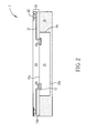
- FIG. 2 is a schematic, cross-sectional view of the fan-out type WLP 1 taken along line I-I' of FIG. 1 .
- the fan-out type WLP 1 comprises a semiconductor die 10 having an active die face 10a and a backside surface 10b.
- a plurality of input/output (I/O) pads 12 are provided on the active die face 10 of the semiconductor die 10.
- the I/O pads 12 may be disposed along the four sides of the semiconductor die 10 in multiple rows, for example, three rows.
- the number of rows of the I/O pads 12 is only for illustration purposes.
- the I/O pads 12 may be arranged in two rows or in four rows in other embodiments.
- the I/O pads 12 are arranged on the active die face 10a in close proximity to each other with a tight pad pitch that may be beyond the limit of an advanced wire bonder.
- the present invention aims to cope with this problem arose from die shrink.
- a support structure 16 may be provided to encompass the semiconductor die 10.
- the support structure 16 comprises molding compounds.
- the support structure 16 may have a top surface 16a that is substantially flush with the active die face 10a.
- the support structure 16 encapsulates the whole surfaces of the semiconductor die 10 except for the active die face 10a where the I/O pads 12 are formed.
- a rewiring laminate structure 20 is provided on the active die face 10a and also on the top surface 1 6a of the support structure 16.
- the rewiring laminate structure 20 comprises a re-routed metal layer 21 formed in a dielectric layer 24 such as silicon oxide, silicon nitride, polyimide, benzocyclobutane (BCB)-based polymer dielectric, a combination thereof, or any other suitable materials.
- the re-routed metal layer 21 may be made of copper, aluminum, a combination thereof, or any other suitable materials.
- the re-routed metal layer 21 in the rewiring laminate structure 20 redistributes the I/O pads 12 in or on the semiconductor die 10 to form redistribution bond pads 22 in or on the dielectric layer 24.
- the redistribution bond pads 22 may be made of copper, aluminum, titanium, nickel, vanadium, a combination thereof, or any other suitable materials.
- the I/O pads 12 may be made of copper, aluminum, a combination thereof, or any other suitable materials.
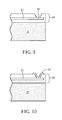
- FIG. 9 and FIG. 10 illustrate some variants of the redistribution bond pads 22, wherein the redistribution bond pad 22 may be a part of the re-routed metal layer 21 as shown in FIG. 9 , or the in combination with other material layer as shown in FIG. 10 .
- the plurality of redistribution bond pads 22 may be arranged in multiple rows, for example, two or three rows, and the plurality of redistribution bond pads 22 may project beyond a die edge 10c of the semiconductor die 10. In another embodiment, only a portion of the redistribution bond pads 22 projects beyond the die edge 10c. In another embodiment, at least a portion of the redistribution bond pads 22 do not project beyond the die edge 10c. In yet another embodiment, there may not be redistribution bond pads 22 projecting beyond the die edge 10c. It is to be understood that the number of rows of the I/O pads 12 may be different from the number of rows of the redistribution bond pads 22. For example, the I/O pads 12 could be arranged in four rows while the redistribution bond pads 22 could be arranged in three rows.
- the semiconductor die 10 may be a power management unit or a power IC, wherein some of the power or ground pads, which are arranged in an inner row on the active die face 10a, may be redistributed to the outer row or the outmost row of the multiple rows of the redistribution bond pads 22 on the dielectric layer 24 by way of the rewiring laminate structure 20.
- the pads may be redistributed to best accommodate package and performance requirements.
- FIG. 3 is a flow diagram depicting the exemplary steps for manufacturing the fan-out WLP 1 of FIG. 2 .
- the fan-out WLP 1 of FIG. 1 can be manufactured by several stages including wafer dicing (Step 51), wafer reconfiguration (Step 52), redistribution (Step 53), and package singulation (Step 54).
- a polishing process (Step 55) may be carried out to remove a portion of the molding compound, thereby exposing the backside surface 10b of the semiconductor die 10.
- Step 55 may be omitted if the backside surface 10b has been exposed during steps 51-54 or if it is decided not to be exposed.
- the fan-out WLP can be manufactured by other methods. Different companies using redistribution technique implement the fan-out WLP using different materials and processes. Nonetheless, the steps required are somewhat similar.
- Redistribution layer technique extends the conventional wafer fabrication process with an additional step that deposits a conductive rerouting and interconnection system to each device, e.g. chip, on the wafer. This is achieved using the similar and compatible photolithography and thin film deposition techniques employed in the device fabrication itself. This additional level of interconnection redistributes the peripheral contact pads of each chip to an area array of conductive pads that are deployed over the chip's surface.
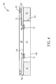
- FIG. 4 is a schematic, cross-sectional diagram showing another exemplary fan-out type WLP 1a in accordance with another embodiment of this invention.
- the fan-out type WLP 1a comprises a semiconductor die 10 having an active die face 10a and a backside surface 10b.
- a plurality of I/O pads 12 such as aluminum bond pads may be provided on the active die face 10a of the semiconductor die 10.
- the I/O pads 12 may be disposed along the four die edges 10c of the semiconductor die 10.
- a support structure 16 could be provided to encompass the semiconductor die 10.
- the support structure 16 may comprise molding compounds with good mechanical strength and superior adhesion ability to the semiconductor die 10.
- the support structure 16 may have a top surface 16a that is substantially flush with the die face 10a.
- the support structure 16 merely covers the die edges 10c of the semiconductor die 10.
- the backside surface 10b is exposed and is not covered with the support structure 16.
- a rewiring laminate structure 20 is provided on the active die face 10a and on the top surface 16a of the support structure 16.
- the rewiring laminate structure 20 comprises a re-routed metal layer 21 formed in a dielectric layer 24.
- the re-routed metal layer 21 in the rewiring laminate structure 12 redistributes the I/O pads 12 in or on the semiconductor die 10 to form redistribution bond pads 22 in or on the dielectric layer 24.
- FIG. 5 is a schematic, cross-sectional diagram showing an exemplary wire bond chip package 100 in accordance with yet another embodiment of this invention.
- a semiconductor die 10 having a die face 10a and a die edge 10c is mounted on a die attach surface 40a of a chip carrier 40 such as a package substrate or a printed circuit board, wherein a plurality of I/O pads 12 are situated in or on the semiconductor die 10.
- a support structure 16 may encompass the semiconductor die 10.
- the support structure 16 may have a top surface 1 6a that is substantially flush with the die face 10a.
- a rewiring laminate structure 20 is provided on the semiconductor die 10.
- the rewiring laminate structure 20 comprises a plurality of redistribution bond pads 22 that may or may not project beyond the die edge 10c.
- a plurality of bond wires 50 are used to interconnect the redistribution bond pads 22 with the corresponding bond pads 42 on the chip carrier 40.
- a mold cap 60 may be provided to encapsulate at least the semiconductor die 10, the rewiring laminate structure 20, the support structure 16 and the bond wires 50. According to this embodiment, the mold cap 60 and the support structure 16 may be made of different molding compounds.
- the bond wires 50 may comprise gold, copper, a combination thereof, or any other suitable materials.
- the redistribution bond pads 22 are made of copper and the bond wires 50 are copper wires.
- the redistribution bond pads 22 thus have a looser pad pitch for wire bonding applications.
- the redistribution bond pads 22 may or may not project beyond the die edge 10c depending upon the design requirements.
- FIG. 6 is a schematic, cross-sectional diagram showing an exemplary wire bond chip package 100a in accordance with yet another embodiment of this invention.
- a fan-out WLP 1 a including a semiconductor die 10 having a die face 10a and a die edge 10c is mounted on a die attach surface or die pad 140a of a chip carrier such as a leadframe 140 by an adhesive layer 152, wherein a plurality of I/O pads 12 are situated in or on the semiconductor die 10.
- the fan-out WLP 1 a may include a support structure 16 encompassing the semiconductor die 10.
- the support structure 16 may have a top surface 1 6a being substantially flush with the die face 10a.
- the fan-out WLP 1 a further includes a rewiring laminate structure 20 that is fabricated on the semiconductor die 10 and on the top surface 16a of the support structure 16.
- the rewiring laminate structure 20 may be fabricated in an assembly house.
- the rewiring laminate structure 20 comprises a plurality of redistribution bond pads 22 that may project beyond the die edge 10c and the redistribution bond pads 22 may have a looser pad pitch for wire bonding applications.
- the redistribution bond pads 22 may not project beyond the die edge 10c, or only a portion of the redistribution bond pads 22 project beyond the die edge 10r.
- at least a portion of the redistribution bond pads 22 do not project beyond the die edge 10c.
- a plurality of bond wires 50 are used to interconnect the redistribution bond pads 22 with the corresponding inner leads 142 of the leadframe 140.
- a mold cap 60 may be provided to encapsulate at least the semiconductor die 10, the rewiring laminate structure 20, the support structure 16, the die pad 140a, the inner leads 142 and the bond wires 50.
- the bond wires 50 may comprise gold, copper, a combination thereof, or any other suitable materials.
- FIG. 7 is a schematic, cross-sectional diagram showing an exemplary wire bond chip package 100b in accordance with yet another embodiment of this invention.
- a fan-out WLP 1 a including a semiconductor die 10 having a die face 10a and a die edge 10c is mounted on a die pad 140a of a leadframe 140 by an adhesive layer 152, wherein a plurality of I/O pads 12 are situated in or on the semiconductor die 10.
- the fan-out WLP 1 a may include a support structure 16 encompassing the semiconductor die 10.
- the support structure 16 may have a top surface 16a being substantially flush with the die face 10a.
- the fan-out WLP 1 a further includes a rewiring laminate structure 20 provided on the semiconductor die 10 and on the top surface 16a of the support structure 16.
- the rewiring laminate structure 20 comprises a plurality of redistribution bond pads 22 that may or may not project beyond the die edge 10c.
- a plurality of bond wires 50 are used to interconnect the redistribution bond pads 22 with the corresponding inner leads 142 of the leadframe 140.
- the bond wires 50 may comprise gold, copper, a combination thereof, or any other suitable materials.
- a mold cap 60 may be provided to encapsulate at least the semiconductor die 10, the rewiring laminate structure 20, the support structure 16, the inner leads 142 and the bond wires 50.
- a bottom surface 140b of the die pad 140a is not encapsulated by the mold cap 60 and is thus exposed to air.
- Such package configuration can be referred to as an exposed-pad (E-pad) low-profile quad flat package (LQFP).
- FIG. 8 is a schematic, cross-sectional diagram showing an exemplary wire bond chip package 100c in accordance with yet another embodiment of this invention.
- a fan-out WLP 1 a including a semiconductor die 10 having a die face 10a and a die edge 10c is mounted on a die pad 240a of a leadframe 240, wherein a plurality of I/O pads 12 are situated in or on the semiconductor die 10.
- the die pad 240a may further include a recess 240c and the semiconductor die 10 may be mounted within the recess 240c.
- the fan-out WLP 1 a may include a support structure 16 encompassing the semiconductor die 10.
- the support structure 16 may have a top surface 16a being substantially flush with the die face 10a.
- the fan-out WLP 1 a further includes a rewiring laminate structure 20 provided on the semiconductor die 10.
- the rewiring laminate structure 20 comprises a plurality of redistribution bond pads 22 that may or may not project beyond the die edge 10c.
- a plurality of bond wires 50 are used to interconnect the redistribution bond pads 22 with the corresponding interconnection pads 242 of the leadframe 240.
- the bond wires 50 may comprise gold, copper, a combination thereof, or any other suitable materials.
- a mold cap 60 may be provided to encapsulate at least the semiconductor die 10, the rewiring laminate structure 20, the support structure 16, the upper portion of the die pad 240a, the upper portion of the interconnection pads 242 and the bond wires 50.
- the package configuration as depicted in FIG. 8 can be referred to as a quad flat non-leaded (QFN) package or an advanced QFN (aQFN) package.
- the support structure 16 shown in FIGS. 2 and 4 -10 may be omitted.
- the another semiconductor die may be coupled to the semiconductor die 10 by at least a bond wire.
- the another semiconductor die may be coupled to a redistribution bond pads 22 of the semiconductor die 10 that does not project beyond the die edge 10c.
Landscapes
- Wire Bonding (AREA)
- Internal Circuitry In Semiconductor Integrated Circuit Devices (AREA)
- Semiconductor Integrated Circuits (AREA)
Abstract
Description
- This application claims the benefit of
U. S. provisional application No. 61 /154,019 filed February 20, 2009 - The present invention relates to a wire bond chip package according to the precharacterizing clauses of
claim 1. - As known in the art, there are a variety of chip package techniques such as ball grid array (BGA), wire bonding, flip-chip, etc. for mounting a die on a substrate via the bonding points on both the die and the substrate. In order to ensure miniaturization and multi-functionality of electronic products or communication devices, semiconductor packages are required to be of small in size, multi-pin connection, high speed, and high functionality.
- Driven by growing demand for smaller, faster and cheaper electronic devices, the semiconductor industry continues to push inexpensive wire bonding technology to higher and higher levels. Nevertheless, for higher (input/output) I/O and higher clock speed the flip chip technology has become the technology of choice. This trend is reflected by that not only the majority of the microprocessors, but also high end ASICs and DSPs are being assembled today using flip chip technology. Still, the mainstream packages continue to be wire bonded - as the price advantages for devices with less than 500 I/O is significant. While the flip chip assembly benefits high performing devices, its cost is the major challenge for main stream applications. Thus, major efforts continue to be made to reduce costs.
- Production cost, packaged device performance and overall size determine the choice between flip chip and wire bonding for IC interconnecting. The biggest advantage of wire bonding is its process flexibility and the sheer quantity of wire bonders in use today. As a consequence, it is a mature technology and the production process is thoroughly researched and well understood. Therefore, wire bonders are a commodity, unlike the advanced die attach platforms for flip chip bonding. In addition, the wire bonding technology is flexible. New package designs and tighter control of wire length in high frequency applications have further expanded the electrical performance range of wire bonded packages.
- However, as the die size shrinks dramatically with the rapid advances in semiconductor manufacturing technologies in the last decade, seemingly, the I/O bond pad pitch on the die has reached the limits of the wire bonder. Therefore, there is a need in the industry for providing an improved package structure in order to extend the life of the wire bonding technology into next-generation technology nodes (e.g. under 55nm) and to cope with the problem of bond pad pitch limit arose from die shrink.
- This in mind, the present invention aims at providing a novel wire bond chip package capable of extending the life of the wire bonding technology into next-generation technology nodes.
- It is another objective to provide an improved wire bond chip package in order to cope with the problem of bond pad pitch limit arose from die shrink.
- This is achieved by a wire bond chip package according to
claim 1. The dependent claims pertain to corresponding further developments and improvements. - As will be seen more clearly from the detailed description below, the claimed wire bond chip package comprises a chip carrier; a semiconductor die having a die face and a die edge, the semiconductor die being mounted on a die attach surface of the chip carrier, wherein a plurality of input/output (I/O) pads are situated in or on the semiconductor die; a rewiring laminate structure on the semiconductor die, the rewiring laminate structure comprising a plurality of redistribution bond pads; a plurality of bond wires interconnecting the redistribution bond pads with the chip carrier; and a mold cap encapsulating at least the semiconductor die and the bond wires.
- In one aspect, a wire bond chip package includes a chip carrier; a semiconductor die having a die face and a die edge, the semiconductor die being mounted on a die attach surface of the chip carrier, wherein a plurality of input/output (I/O) pads are situated in or on the semiconductor die; a support structure encompassing the semiconductor die; a rewiring laminate structure on the semiconductor die, the rewiring laminate structure comprising a plurality of redistribution bond pads; a plurality of bond wires interconnecting the redistribution bond pads with the chip carrier; and a mold cap encapsulating at least the semiconductor die, the rewiring laminate structure, the support structure and the bond wires.
- In the following, the invention is further illustrated by way of example, taking reference to the accompanying drawings. Thereof:
-
FIG. 1 is a schematic plan view of an exemplary fan-out type wafer level package (WLP) in accordance with one embodiment of this invention. -
FIG. 2 is a schematic, cross-sectional view of the fan-out type WLP taken along line I-I' ofFIG. 1 . -
FIG. 3 is a flow diagram depicting the exemplary steps for manufacturing the fan-out WLP ofFIG. 2 . -
FIG. 4 is a schematic, cross-sectional diagram showing another exemplary fan-out type WLP in accordance with another embodiment of this invention. -
FIG. 5 is a schematic, cross-sectional diagram showing an exemplary wire bond chip package in accordance with yet another embodiment of this invention. -
FIG. 6 is a schematic, cross-sectional diagram showing an exemplary wire bond chip package in accordance with yet another embodiment of this invention. -
FIG. 7 is a schematic, cross-sectional diagram showing an exemplary wire bond chip package in accordance with yet another embodiment of this invention. -
FIG. 8 is a schematic, cross-sectional diagram showing an exemplary wire bond chip package in accordance with yet another embodiment of this invention. -
FIG. 9 and FIG.10 illustrate variants of the redistribution bond pad in cross-sectional views according to this invention. - In the following description, numerous specific details are given to provide a thorough understanding of the invention. However, it will be apparent to one skilled in the art that the invention may be practiced without these specific details. In order to avoid obscuring the present invention, some well-known system configurations and process steps are not disclosed in detail.
- Likewise, the drawings showing embodiments of the apparatus are semi-diagrammatic and not to scale and, particularly, some of the dimensions are for the clarity of presentation and are shown exaggerated in the FIGS. Also, where multiple embodiments are disclosed and described having some features in common, for clarity and ease of illustration and description thereof like or similar features one to another will ordinarily be described with like reference numerals.
-
FIG. 1 is a schematic plan view of an exemplary fan-out type wafer level package (WLP) 1 in accordance with one embodiment of this invention.FIG. 2 is a schematic, cross-sectional view of the fan-outtype WLP 1 taken along line I-I' ofFIG. 1 . As shown inFIG. 1 andFIG. 2 , the fan-out type WLP 1 comprises asemiconductor die 10 having anactive die face 10a and abackside surface 10b. A plurality of input/output (I/O)pads 12 are provided on theactive die face 10 of the semiconductor die 10. As can be best seen inFIG. 1 , the I/O pads 12 may be disposed along the four sides of the semiconductor die 10 in multiple rows, for example, three rows. - Of course, the number of rows of the I/
O pads 12 is only for illustration purposes. For example, the I/O pads 12 may be arranged in two rows or in four rows in other embodiments. The I/O pads 12 are arranged on theactive die face 10a in close proximity to each other with a tight pad pitch that may be beyond the limit of an advanced wire bonder. The present invention aims to cope with this problem arose from die shrink. - As can be best seen in
FIG. 2 , asupport structure 16 may be provided to encompass thesemiconductor die 10. Preferably, thesupport structure 16 comprises molding compounds. Thesupport structure 16 may have atop surface 16a that is substantially flush with theactive die face 10a. By way of example, thesupport structure 16 encapsulates the whole surfaces of thesemiconductor die 10 except for theactive die face 10a where the I/O pads 12 are formed. - Still referring to
FIG. 2 , a rewiringlaminate structure 20 is provided on theactive die face 10a and also on thetop surface 1 6a of thesupport structure 16. The rewiringlaminate structure 20 comprises a re-routedmetal layer 21 formed in adielectric layer 24 such as silicon oxide, silicon nitride, polyimide, benzocyclobutane (BCB)-based polymer dielectric, a combination thereof, or any other suitable materials. The re-routedmetal layer 21 may be made of copper, aluminum, a combination thereof, or any other suitable materials. The re-routedmetal layer 21 in the rewiringlaminate structure 20 redistributes the I/O pads 12 in or on the semiconductor die 10 to formredistribution bond pads 22 in or on thedielectric layer 24. According to one embodiment of this invention, theredistribution bond pads 22 may be made of copper, aluminum, titanium, nickel, vanadium, a combination thereof, or any other suitable materials. The I/O pads 12 may be made of copper, aluminum, a combination thereof, or any other suitable materials. It is to be understood that the sectional structure of theredistribution bond pads 22 as depicted throughFIG. 2-8 are for illustration purposes only. Other configurations of theredistribution bond pads 22 providing coupling to the I/O pads 12 may be used. For example,FIG. 9 and FIG. 10 illustrate some variants of theredistribution bond pads 22, wherein theredistribution bond pad 22 may be a part of the re-routedmetal layer 21 as shown inFIG. 9 , or the in combination with other material layer as shown inFIG. 10 . - According to the embodiment of this invention, the plurality of
redistribution bond pads 22 may be arranged in multiple rows, for example, two or three rows, and the plurality ofredistribution bond pads 22 may project beyond adie edge 10c of the semiconductor die 10. In another embodiment, only a portion of the redistribution bond pads 22 projects beyond the dieedge 10c. In another embodiment, at least a portion of theredistribution bond pads 22 do not project beyond the dieedge 10c. In yet another embodiment, there may not beredistribution bond pads 22 projecting beyond thedie edge 10c. It is to be understood that the number of rows of the I/O pads 12 may be different from the number of rows of theredistribution bond pads 22. For example, the I/O pads 12 could be arranged in four rows while theredistribution bond pads 22 could be arranged in three rows. - According to another embodiment of this invention, the semiconductor die 10 may be a power management unit or a power IC, wherein some of the power or ground pads, which are arranged in an inner row on the
active die face 10a, may be redistributed to the outer row or the outmost row of the multiple rows of theredistribution bond pads 22 on thedielectric layer 24 by way of therewiring laminate structure 20. By doing this, the chip performance can be enhanced. In other words, with this invention, the pads may be redistributed to best accommodate package and performance requirements. -
FIG. 3 is a flow diagram depicting the exemplary steps for manufacturing the fan-outWLP 1 ofFIG. 2 . As shown inFIG. 3 , the fan-outWLP 1 ofFIG. 1 can be manufactured by several stages including wafer dicing (Step 51), wafer reconfiguration (Step 52), redistribution (Step 53), and package singulation (Step 54). After the package singulation, optionally, a polishing process (Step 55) may be carried out to remove a portion of the molding compound, thereby exposing thebackside surface 10b of the semiconductor die 10.Step 55 may be omitted if thebackside surface 10b has been exposed during steps 51-54 or if it is decided not to be exposed. It is understood that the fan-out WLP can be manufactured by other methods. Different companies using redistribution technique implement the fan-out WLP using different materials and processes. Nonetheless, the steps required are somewhat similar. - Redistribution layer technique extends the conventional wafer fabrication process with an additional step that deposits a conductive rerouting and interconnection system to each device, e.g. chip, on the wafer. This is achieved using the similar and compatible photolithography and thin film deposition techniques employed in the device fabrication itself. This additional level of interconnection redistributes the peripheral contact pads of each chip to an area array of conductive pads that are deployed over the chip's surface.
-
FIG. 4 is a schematic, cross-sectional diagram showing another exemplary fan-out type WLP 1a in accordance with another embodiment of this invention. As shown inFIG. 4 , likewise, the fan-out type WLP 1a comprises asemiconductor die 10 having anactive die face 10a and abackside surface 10b. A plurality of I/O pads 12 such as aluminum bond pads may be provided on theactive die face 10a of the semiconductor die 10. The I/O pads 12 may be disposed along the fourdie edges 10c of the semiconductor die 10. - A
support structure 16 could be provided to encompass the semiconductor die 10. Preferably, thesupport structure 16 may comprise molding compounds with good mechanical strength and superior adhesion ability to the semiconductor die 10. Thesupport structure 16 may have atop surface 16a that is substantially flush with thedie face 10a. In this embodiment, thesupport structure 16 merely covers the die edges 10c of the semiconductor die 10. Thebackside surface 10b is exposed and is not covered with thesupport structure 16. - Likewise, a
rewiring laminate structure 20 is provided on theactive die face 10a and on thetop surface 16a of thesupport structure 16. Therewiring laminate structure 20 comprises are-routed metal layer 21 formed in adielectric layer 24. There-routed metal layer 21 in therewiring laminate structure 12 redistributes the I/O pads 12 in or on the semiconductor die 10 to formredistribution bond pads 22 in or on thedielectric layer 24. -
FIG. 5 is a schematic, cross-sectional diagram showing an exemplary wirebond chip package 100 in accordance with yet another embodiment of this invention. As shown inFIG. 5 , asemiconductor die 10 having adie face 10a and adie edge 10c is mounted on a die attachsurface 40a of achip carrier 40 such as a package substrate or a printed circuit board, wherein a plurality of I/O pads 12 are situated in or on the semiconductor die 10. Asupport structure 16 may encompass the semiconductor die 10. Thesupport structure 16 may have atop surface 1 6a that is substantially flush with thedie face 10a. - A
rewiring laminate structure 20 is provided on the semiconductor die 10. Therewiring laminate structure 20 comprises a plurality ofredistribution bond pads 22 that may or may not project beyond thedie edge 10c. A plurality ofbond wires 50 are used to interconnect theredistribution bond pads 22 with thecorresponding bond pads 42 on thechip carrier 40. Amold cap 60 may be provided to encapsulate at least the semiconductor die 10, therewiring laminate structure 20, thesupport structure 16 and thebond wires 50. According to this embodiment, themold cap 60 and thesupport structure 16 may be made of different molding compounds. - According to this embodiment, the
bond wires 50 may comprise gold, copper, a combination thereof, or any other suitable materials. According to one embodiment of this invention, theredistribution bond pads 22 are made of copper and thebond wires 50 are copper wires. - Since the I/
O pads 12 on the semiconductor die 10 with tighter pad pitches are redistributed to a peripheral, outer area that projects beyond thedie edge 10c, theredistribution bond pads 22 thus have a looser pad pitch for wire bonding applications. However, as previously mentioned, theredistribution bond pads 22 may or may not project beyond thedie edge 10c depending upon the design requirements. -
FIG. 6 is a schematic, cross-sectional diagram showing an exemplary wirebond chip package 100a in accordance with yet another embodiment of this invention. As shown inFIG. 6 , a fan-out WLP 1 a including asemiconductor die 10 having adie face 10a and adie edge 10c is mounted on a die attach surface or diepad 140a of a chip carrier such as aleadframe 140 by anadhesive layer 152, wherein a plurality of I/O pads 12 are situated in or on the semiconductor die 10. The fan-out WLP 1 a may include asupport structure 16 encompassing the semiconductor die 10. Thesupport structure 16 may have atop surface 1 6a being substantially flush with thedie face 10a. - The fan-out WLP 1 a further includes a
rewiring laminate structure 20 that is fabricated on the semiconductor die 10 and on thetop surface 16a of thesupport structure 16. Therewiring laminate structure 20 may be fabricated in an assembly house. Therewiring laminate structure 20 comprises a plurality ofredistribution bond pads 22 that may project beyond thedie edge 10c and theredistribution bond pads 22 may have a looser pad pitch for wire bonding applications. In another embodiment, depending upon the design requirements, theredistribution bond pads 22 may not project beyond thedie edge 10c, or only a portion of theredistribution bond pads 22 project beyond the die edge 10r. In yet another embodiment, at least a portion of theredistribution bond pads 22 do not project beyond thedie edge 10c. - A plurality of
bond wires 50 are used to interconnect theredistribution bond pads 22 with the corresponding inner leads 142 of theleadframe 140. Amold cap 60 may be provided to encapsulate at least the semiconductor die 10, therewiring laminate structure 20, thesupport structure 16, thedie pad 140a, the inner leads 142 and thebond wires 50. According to this embodiment, thebond wires 50 may comprise gold, copper, a combination thereof, or any other suitable materials. -
FIG. 7 is a schematic, cross-sectional diagram showing an exemplary wirebond chip package 100b in accordance with yet another embodiment of this invention. As shown inFIG. 7 , a fan-out WLP 1 a including asemiconductor die 10 having adie face 10a and adie edge 10c is mounted on adie pad 140a of aleadframe 140 by anadhesive layer 152, wherein a plurality of I/O pads 12 are situated in or on the semiconductor die 10. The fan-out WLP 1 a may include asupport structure 16 encompassing the semiconductor die 10. Thesupport structure 16 may have atop surface 16a being substantially flush with thedie face 10a. The fan-out WLP 1 a further includes arewiring laminate structure 20 provided on the semiconductor die 10 and on thetop surface 16a of thesupport structure 16. Likewise, therewiring laminate structure 20 comprises a plurality ofredistribution bond pads 22 that may or may not project beyond thedie edge 10c. - A plurality of
bond wires 50 are used to interconnect theredistribution bond pads 22 with the corresponding inner leads 142 of theleadframe 140. Thebond wires 50 may comprise gold, copper, a combination thereof, or any other suitable materials. Amold cap 60 may be provided to encapsulate at least the semiconductor die 10, therewiring laminate structure 20, thesupport structure 16, the inner leads 142 and thebond wires 50. According to this embodiment, abottom surface 140b of thedie pad 140a is not encapsulated by themold cap 60 and is thus exposed to air. Such package configuration can be referred to as an exposed-pad (E-pad) low-profile quad flat package (LQFP). -
FIG. 8 is a schematic, cross-sectional diagram showing an exemplary wirebond chip package 100c in accordance with yet another embodiment of this invention. As shown inFIG. 8 , a fan-out WLP 1 a including asemiconductor die 10 having adie face 10a and adie edge 10c is mounted on adie pad 240a of aleadframe 240, wherein a plurality of I/O pads 12 are situated in or on the semiconductor die 10. Thedie pad 240a may further include arecess 240c and the semiconductor die 10 may be mounted within therecess 240c. The fan-out WLP 1 a may include asupport structure 16 encompassing the semiconductor die 10. Thesupport structure 16 may have atop surface 16a being substantially flush with thedie face 10a. The fan-out WLP 1 a further includes arewiring laminate structure 20 provided on the semiconductor die 10. Therewiring laminate structure 20 comprises a plurality ofredistribution bond pads 22 that may or may not project beyond thedie edge 10c. - A plurality of
bond wires 50 are used to interconnect theredistribution bond pads 22 with thecorresponding interconnection pads 242 of theleadframe 240. Thebond wires 50 may comprise gold, copper, a combination thereof, or any other suitable materials. Amold cap 60 may be provided to encapsulate at least the semiconductor die 10, therewiring laminate structure 20, thesupport structure 16, the upper portion of thedie pad 240a, the upper portion of theinterconnection pads 242 and thebond wires 50. The package configuration as depicted inFIG. 8 can be referred to as a quad flat non-leaded (QFN) package or an advanced QFN (aQFN) package. - In other embodiments, the
support structure 16 shown inFIGS. 2 and4 -10 may be omitted. In yet other embodiments, there may be another semiconductor die on or over the semiconductor die 10. The another semiconductor die may be coupled to the semiconductor die 10 by at least a bond wire. In yet other embodiments, the another semiconductor die may be coupled to aredistribution bond pads 22 of the semiconductor die 10 that does not project beyond thedie edge 10c.
Claims (15)
- A wire bond chip package (100, 100a, 100b, 100c), comprising:a chip carrier (40, 140, 240);a semiconductor die (10) mounted on a die attach surface (40a, 140a) of the chip carrier (40, 140, 240), wherein a plurality of input/output (I/O) pads (12) are situated in or on the semiconductor die (10);a rewiring laminate structure (20) on the semiconductor die (10), the rewiring laminate structure (20) comprising a plurality of redistribution bond pads (22);a plurality of bond wires (50) interconnecting the redistribution bond pads (22) with the chip carrier (40, 140, 240); anda mold cap (60) encapsulating at least the semiconductor die (10) and the bond wires (50).
- The wire bond chip package (100, 100a, 100b, 100c) according to claim 1 wherein the chip carrier (40) is a package substrate.
- The wire bond chip package (100, 100a, 100b, 100c) according to claim 1 wherein the chip carrier (40) is a printed circuit board.
- The wire bond chip package (100, 100a, 100b, 100c) according to claim 1 wherein the chip carrier (140, 240) is a leadframe.
- The wire bond chip package (100, 100a, 100b, 100c) according to claim 4 wherein the wire bond chip package is a low-profile quad flat package (LQFP).
- The wire bond chip package (100, 100a, 100b, 100c) according to claim 4 wherein the wire bond chip package is a quad flat non-leaded (QFN) package.
- The wire bond chip package (100, 100a, 100b, 100c) according to claim 1 wherein the bond wires (50) are gold wires.
- The wire bond chip package (100, 100a, 100b, 100c) according to claim 1 wherein the bond wires (50) are copper wires.
- The wire bond chip package (100, 100a, 100b, 100c) according to claim 1 wherein at least one of the redistribution bond pads (22) project beyond the die edge (1 0c) of the semiconductor die (10).
- The wire bond chip package (100, 100a, 100b, 100c) according to claim 1 , further comprising:a support structure (16) encompassing the semiconductor die (10);wherein the mold cap (60) encapsulates at least the semiconductor die (10), the rewiring laminate structure (20), the support structure (16) and the bond wires (50).
- The wire bond chip package (100, 100a, 100b, 100c) according to claim 10 wherein a top surface (1 6a) of the support structure (16) is substantially flush with a die face (10a).
- The wire bond chip package (100, 100a, 100b, 100c) according to claim 11 wherein the rewiring laminate structure (20) is also formed on the top surface (16a) of the support structure (16).
- The wire bond chip package (100, 100a, 100b, 100c) according to claim 10 wherein the support structure (16) and the mold cap (60) are made of different molding compounds.
- The wire bond chip package (100, 100a, 100b, 100c) according to claim 10 wherein material of the I/O pads (12) comprises copper, aluminum or a combination thereof..
- The wire bond chip package (100, 100a, 100b, 100c) according to claim 10 wherein material of the redistribution bond pads (22) comprises copper, aluminum, titanium, nickel, vanadium or a combination thereof.
Priority Applications (1)
| Application Number | Priority Date | Filing Date | Title |
|---|---|---|---|
| DE09009506T DE09009506T8 (en) | 2009-02-20 | 2009-07-22 | Wire bond chip package |
Applications Claiming Priority (2)
| Application Number | Priority Date | Filing Date | Title |
|---|---|---|---|
| US15401909P | 2009-02-20 | 2009-02-20 | |
| US12/485,923 US20100213588A1 (en) | 2009-02-20 | 2009-06-17 | Wire bond chip package |
Publications (2)
| Publication Number | Publication Date |
|---|---|
| EP2221869A2 true EP2221869A2 (en) | 2010-08-25 |
| EP2221869A3 EP2221869A3 (en) | 2011-09-21 |
Family
ID=42288853
Family Applications (1)
| Application Number | Title | Priority Date | Filing Date |
|---|---|---|---|
| EP09009506A Withdrawn EP2221869A3 (en) | 2009-02-20 | 2009-07-22 | Wire bond chip package |
Country Status (5)
| Country | Link |
|---|---|
| US (1) | US20100213588A1 (en) |
| EP (1) | EP2221869A3 (en) |
| CN (1) | CN101814474A (en) |
| DE (1) | DE09009506T8 (en) |
| TW (1) | TW201032308A (en) |
Families Citing this family (17)
| Publication number | Priority date | Publication date | Assignee | Title |
|---|---|---|---|---|
| US8310051B2 (en) | 2008-05-27 | 2012-11-13 | Mediatek Inc. | Package-on-package with fan-out WLCSP |
| US8093722B2 (en) * | 2008-05-27 | 2012-01-10 | Mediatek Inc. | System-in-package with fan-out WLCSP |
| US8288209B1 (en) * | 2011-06-03 | 2012-10-16 | Stats Chippac, Ltd. | Semiconductor device and method of using leadframe bodies to form openings through encapsulant for vertical interconnect of semiconductor die |
| DE102013202904A1 (en) * | 2013-02-22 | 2014-08-28 | Osram Opto Semiconductors Gmbh | Optoelectronic semiconductor component and method for its production |
| US20150054099A1 (en) * | 2013-08-25 | 2015-02-26 | Kai Yun Yow | Pressure sensor device and assembly method |
| US10103128B2 (en) | 2013-10-04 | 2018-10-16 | Mediatek Inc. | Semiconductor package incorporating redistribution layer interposer |
| US9165877B2 (en) * | 2013-10-04 | 2015-10-20 | Mediatek Inc. | Fan-out semiconductor package with copper pillar bumps |
| US10074628B2 (en) | 2013-10-04 | 2018-09-11 | Mediatek Inc. | System-in-package and fabrication method thereof |
| US9859265B2 (en) | 2014-06-06 | 2018-01-02 | Taiwan Semiconductor Manufacturing Company, Ltd. | Package structure and methods of forming the same |
| KR101685068B1 (en) * | 2015-04-03 | 2016-12-21 | 주식회사 네패스 | System in package and method for manufacturing the same |
| US9842820B1 (en) * | 2015-12-04 | 2017-12-12 | Altera Corporation | Wafer-level fan-out wirebond packages |
| CN105845672B (en) * | 2016-06-15 | 2018-10-23 | 通富微电子股份有限公司 | Encapsulating structure |
| CN105895541B (en) * | 2016-06-15 | 2018-10-23 | 通富微电子股份有限公司 | The forming method of encapsulating structure |
| IT201600086488A1 (en) * | 2016-08-22 | 2018-02-22 | St Microelectronics Srl | SEMICONDUCTOR DEVICE AND CORRESPONDENT PROCEDURE |
| CN108010898A (en) * | 2017-11-02 | 2018-05-08 | 上海玮舟微电子科技有限公司 | A kind of chip-packaging structure |
| US20200161206A1 (en) * | 2018-11-20 | 2020-05-21 | Advanced Semiconductor Engineering, Inc. | Semiconductor package structure and semiconductor manufacturing process |
| US20220254707A1 (en) * | 2019-07-25 | 2022-08-11 | Samtec, Inc. | Wirebondable interposer for flip chip packaged integrated circuit die |
Citations (1)
| Publication number | Priority date | Publication date | Assignee | Title |
|---|---|---|---|---|
| US20070262436A1 (en) * | 2006-05-12 | 2007-11-15 | Micron Technology, Inc. | Microelectronic devices and methods for manufacturing microelectronic devices |
Family Cites Families (30)
| Publication number | Priority date | Publication date | Assignee | Title |
|---|---|---|---|---|
| US4477828A (en) * | 1982-10-12 | 1984-10-16 | Scherer Jeremy D | Microcircuit package and sealing method |
| US5331205A (en) * | 1992-02-21 | 1994-07-19 | Motorola, Inc. | Molded plastic package with wire protection |
| US5438224A (en) * | 1992-04-23 | 1995-08-01 | Motorola, Inc. | Integrated circuit package having a face-to-face IC chip arrangement |
| US5530284A (en) * | 1995-03-06 | 1996-06-25 | Motorola, Inc. | Semiconductor leadframe structure compatible with differing bond wire materials |
| US6528873B1 (en) * | 1996-01-16 | 2003-03-04 | Texas Instruments Incorporated | Ball grid assembly with solder columns |
| US6294407B1 (en) * | 1998-05-06 | 2001-09-25 | Virtual Integration, Inc. | Microelectronic packages including thin film decal and dielectric adhesive layer having conductive vias therein, and methods of fabricating the same |
| US6544880B1 (en) * | 1999-06-14 | 2003-04-08 | Micron Technology, Inc. | Method of improving copper interconnects of semiconductor devices for bonding |
| SG83742A1 (en) * | 1999-08-17 | 2001-10-16 | Micron Technology Inc | Multi-chip module with extension |
| US6867499B1 (en) * | 1999-09-30 | 2005-03-15 | Skyworks Solutions, Inc. | Semiconductor packaging |
| US6198171B1 (en) * | 1999-12-30 | 2001-03-06 | Siliconware Precision Industries Co., Ltd. | Thermally enhanced quad flat non-lead package of semiconductor |
| US6707149B2 (en) * | 2000-09-29 | 2004-03-16 | Tessera, Inc. | Low cost and compliant microelectronic packages for high i/o and fine pitch |
| JP2003115664A (en) * | 2001-10-05 | 2003-04-18 | Matsushita Electric Ind Co Ltd | Voltage conversion module |
| SG104293A1 (en) * | 2002-01-09 | 2004-06-21 | Micron Technology Inc | Elimination of rdl using tape base flip chip on flex for die stacking |
| DE10250538B4 (en) * | 2002-10-29 | 2008-02-21 | Infineon Technologies Ag | Electronic component as multichip module and method for its production |
| DE10255844B3 (en) * | 2002-11-29 | 2004-07-15 | Infineon Technologies Ag | Integrated circuit manufacturing method of chip scale package, involves attaching solder balls in area that is uncovered by resist element, of patterned rewriting element, in patterned form |
| TWI311353B (en) * | 2003-04-18 | 2009-06-21 | Advanced Semiconductor Eng | Stacked chip package structure |
| KR100639948B1 (en) * | 2005-08-22 | 2006-11-01 | 삼성전자주식회사 | Leadframe package with binary lead placement |
| KR101172527B1 (en) * | 2005-03-31 | 2012-08-10 | 스태츠 칩팩, 엘티디. | Semiconductor stacked package assembly having exposed substrate surfaces on upper and lower sides |
| US7326592B2 (en) * | 2005-04-04 | 2008-02-05 | Infineon Technologies Ag | Stacked die package |
| US7354800B2 (en) * | 2005-04-29 | 2008-04-08 | Stats Chippac Ltd. | Method of fabricating a stacked integrated circuit package system |
| US7312519B2 (en) * | 2006-01-12 | 2007-12-25 | Stats Chippac Ltd. | Stacked integrated circuit package-in-package system |
| US7288835B2 (en) * | 2006-03-17 | 2007-10-30 | Stats Chippac Ltd. | Integrated circuit package-in-package system |
| US7535110B2 (en) * | 2006-06-15 | 2009-05-19 | Marvell World Trade Ltd. | Stack die packages |
| US7517733B2 (en) * | 2007-03-22 | 2009-04-14 | Stats Chippac, Ltd. | Leadframe design for QFN package with top terminal leads |
| US7911053B2 (en) * | 2007-04-19 | 2011-03-22 | Marvell World Trade Ltd. | Semiconductor packaging with internal wiring bus |
| CN101312177A (en) * | 2007-05-22 | 2008-11-26 | 飞思卡尔半导体(中国)有限公司 | Lead frames for semiconductor devices |
| US7566966B2 (en) * | 2007-09-05 | 2009-07-28 | Stats Chippac Ltd. | Integrated circuit package-on-package system with anti-mold flash feature |
| US7791209B2 (en) * | 2008-03-12 | 2010-09-07 | International Business Machines Corporation | Method of underfill air vent for flipchip BGA |
| TWI362732B (en) * | 2008-04-07 | 2012-04-21 | Nanya Technology Corp | Multi-chip stack package |
| US7838975B2 (en) * | 2008-05-27 | 2010-11-23 | Mediatek Inc. | Flip-chip package with fan-out WLCSP |
-
2009
- 2009-06-17 US US12/485,923 patent/US20100213588A1/en not_active Abandoned
- 2009-07-22 DE DE09009506T patent/DE09009506T8/en active Active
- 2009-07-22 EP EP09009506A patent/EP2221869A3/en not_active Withdrawn
- 2009-12-17 CN CN200910260366A patent/CN101814474A/en active Pending
- 2009-12-17 TW TW098143346A patent/TW201032308A/en unknown
Patent Citations (1)
| Publication number | Priority date | Publication date | Assignee | Title |
|---|---|---|---|---|
| US20070262436A1 (en) * | 2006-05-12 | 2007-11-15 | Micron Technology, Inc. | Microelectronic devices and methods for manufacturing microelectronic devices |
Also Published As
| Publication number | Publication date |
|---|---|
| EP2221869A3 (en) | 2011-09-21 |
| CN101814474A (en) | 2010-08-25 |
| DE09009506T8 (en) | 2013-04-25 |
| DE09009506T1 (en) | 2012-09-06 |
| US20100213588A1 (en) | 2010-08-26 |
| TW201032308A (en) | 2010-09-01 |
Similar Documents
| Publication | Publication Date | Title |
|---|---|---|
| US20100213588A1 (en) | Wire bond chip package | |
| US20100213589A1 (en) | Multi-chip package | |
| US7326592B2 (en) | Stacked die package | |
| US7476962B2 (en) | Stack semiconductor package formed by multiple molding and method of manufacturing the same | |
| US9761568B2 (en) | Thin fan-out multi-chip stacked packages and the method for manufacturing the same | |
| CN106505045B (en) | Semiconductor package and method with routable encapsulated conductive substrate | |
| CN102456584B (en) | Semiconductor device and method of forming pentrable film encapsulant around semiconductor die and interconnect structure | |
| EP3093877B1 (en) | Semiconductor package | |
| TWI387077B (en) | Grain reconfigurable package structure and method thereof | |
| TWI689017B (en) | Semiconductor device and method of controlling warpage in reconstituted wafer | |
| CN107134438A (en) | Semiconductor device and method of forming insulating layer around semiconductor die | |
| US20200357770A1 (en) | Semiconductor package and manufacturing method thereof | |
| US7598599B2 (en) | Semiconductor package system with substrate having different bondable heights at lead finger tips | |
| CN101621041B (en) | Package structure and method for chip reconfiguration | |
| CN101930971A (en) | Multi-chip packaging structure and method for forming multi-chip packaging structure | |
| CN211929479U (en) | Semiconductor device | |
| US20080290511A1 (en) | Chip Assembly and Method of Manufacturing Thereof | |
| CN207852667U (en) | Fan-out-type antenna packages structure with electromagnetic protection | |
| CN101488462B (en) | Modular multi-die package structure and method thereof | |
| US11869837B2 (en) | Semiconductor device packaging extendable lead and method therefor | |
| CN114284240A (en) | Semiconductor packaging structure | |
| US20060071305A1 (en) | Electrical package structure including chip with polymer thereon | |
| US20070281393A1 (en) | Method of forming a trace embedded package | |
| TWI517334B (en) | Ultra-thin wafer level fan-out package construction | |
| TW201001632A (en) | Chip rearrangement package structure and the method thereof |
Legal Events
| Date | Code | Title | Description |
|---|---|---|---|
| PUAI | Public reference made under article 153(3) epc to a published international application that has entered the european phase |
Free format text: ORIGINAL CODE: 0009012 |
|
| AK | Designated contracting states |
Kind code of ref document: A2 Designated state(s): AT BE BG CH CY CZ DE DK EE ES FI FR GB GR HR HU IE IS IT LI LT LU LV MC MK MT NL NO PL PT RO SE SI SK SM TR |
|
| AX | Request for extension of the european patent |
Extension state: AL BA RS |
|
| PUAL | Search report despatched |
Free format text: ORIGINAL CODE: 0009013 |
|
| AK | Designated contracting states |
Kind code of ref document: A3 Designated state(s): AT BE BG CH CY CZ DE DK EE ES FI FR GB GR HR HU IE IS IT LI LT LU LV MC MK MT NL NO PL PT RO SE SI SK SM TR |
|
| AX | Request for extension of the european patent |
Extension state: AL BA RS |
|
| RIC1 | Information provided on ipc code assigned before grant |
Ipc: H01L 23/498 20060101ALI20110816BHEP Ipc: H01L 23/538 20060101AFI20110816BHEP |
|
| REG | Reference to a national code |
Ref country code: DE Ref legal event code: R082 Ref country code: DE Ref legal event code: R082 Representative=s name: HOEFER & PARTNER, DE Ref country code: DE Ref legal event code: R082 Representative=s name: HOEFER & PARTNER PATENTANWAELTE MBB, DE |
|
| 17P | Request for examination filed |
Effective date: 20120229 |
|
| REG | Reference to a national code |
Ref country code: FR Ref legal event code: EL |
|
| REG | Reference to a national code |
Ref country code: DE Ref legal event code: R210 Effective date: 20120906 |
|
| 17Q | First examination report despatched |
Effective date: 20140331 |
|
| STAA | Information on the status of an ep patent application or granted ep patent |
Free format text: STATUS: THE APPLICATION IS DEEMED TO BE WITHDRAWN |
|
| 18D | Application deemed to be withdrawn |
Effective date: 20140812 |