EP2221858A1 - Semiconductor device - Google Patents
Semiconductor device Download PDFInfo
- Publication number
- EP2221858A1 EP2221858A1 EP07850486A EP07850486A EP2221858A1 EP 2221858 A1 EP2221858 A1 EP 2221858A1 EP 07850486 A EP07850486 A EP 07850486A EP 07850486 A EP07850486 A EP 07850486A EP 2221858 A1 EP2221858 A1 EP 2221858A1
- Authority
- EP
- European Patent Office
- Prior art keywords
- silicon pillar
- silicide
- semiconductor device
- surrounding
- contact
- Prior art date
- Legal status (The legal status is an assumption and is not a legal conclusion. Google has not performed a legal analysis and makes no representation as to the accuracy of the status listed.)
- Withdrawn
Links
Images





Classifications
-
- H—ELECTRICITY
- H10—SEMICONDUCTOR DEVICES; ELECTRIC SOLID-STATE DEVICES NOT OTHERWISE PROVIDED FOR
- H10D—INORGANIC ELECTRIC SEMICONDUCTOR DEVICES
- H10D62/00—Semiconductor bodies, or regions thereof, of devices having potential barriers
- H10D62/80—Semiconductor bodies, or regions thereof, of devices having potential barriers characterised by the materials
- H10D62/83—Semiconductor bodies, or regions thereof, of devices having potential barriers characterised by the materials being Group IV materials, e.g. B-doped Si or undoped Ge
-
- H—ELECTRICITY
- H10—SEMICONDUCTOR DEVICES; ELECTRIC SOLID-STATE DEVICES NOT OTHERWISE PROVIDED FOR
- H10D—INORGANIC ELECTRIC SEMICONDUCTOR DEVICES
- H10D30/00—Field-effect transistors [FET]
- H10D30/01—Manufacture or treatment
- H10D30/021—Manufacture or treatment of FETs having insulated gates [IGFET]
- H10D30/025—Manufacture or treatment of FETs having insulated gates [IGFET] of vertical IGFETs
-
- H—ELECTRICITY
- H10—SEMICONDUCTOR DEVICES; ELECTRIC SOLID-STATE DEVICES NOT OTHERWISE PROVIDED FOR
- H10D—INORGANIC ELECTRIC SEMICONDUCTOR DEVICES
- H10D30/00—Field-effect transistors [FET]
- H10D30/60—Insulated-gate field-effect transistors [IGFET]
- H10D30/63—Vertical IGFETs
-
- H—ELECTRICITY
- H10—SEMICONDUCTOR DEVICES; ELECTRIC SOLID-STATE DEVICES NOT OTHERWISE PROVIDED FOR
- H10D—INORGANIC ELECTRIC SEMICONDUCTOR DEVICES
- H10D30/00—Field-effect transistors [FET]
- H10D30/60—Insulated-gate field-effect transistors [IGFET]
- H10D30/67—Thin-film transistors [TFT]
- H10D30/6729—Thin-film transistors [TFT] characterised by the electrodes
- H10D30/673—Thin-film transistors [TFT] characterised by the electrodes characterised by the shapes, relative sizes or dispositions of the gate electrodes
- H10D30/6735—Thin-film transistors [TFT] characterised by the electrodes characterised by the shapes, relative sizes or dispositions of the gate electrodes having gates fully surrounding the channels, e.g. gate-all-around
-
- H—ELECTRICITY
- H10—SEMICONDUCTOR DEVICES; ELECTRIC SOLID-STATE DEVICES NOT OTHERWISE PROVIDED FOR
- H10D—INORGANIC ELECTRIC SEMICONDUCTOR DEVICES
- H10D62/00—Semiconductor bodies, or regions thereof, of devices having potential barriers
- H10D62/10—Shapes, relative sizes or dispositions of the regions of the semiconductor bodies; Shapes of the semiconductor bodies
- H10D62/117—Shapes of semiconductor bodies
-
- H—ELECTRICITY
- H10—SEMICONDUCTOR DEVICES; ELECTRIC SOLID-STATE DEVICES NOT OTHERWISE PROVIDED FOR
- H10D—INORGANIC ELECTRIC SEMICONDUCTOR DEVICES
- H10D64/00—Electrodes of devices having potential barriers
- H10D64/20—Electrodes characterised by their shapes, relative sizes or dispositions
- H10D64/23—Electrodes carrying the current to be rectified, amplified, oscillated or switched, e.g. sources, drains, anodes or cathodes
- H10D64/251—Source or drain electrodes for field-effect devices
- H10D64/252—Source or drain electrodes for field-effect devices for vertical or pseudo-vertical devices
-
- H—ELECTRICITY
- H10—SEMICONDUCTOR DEVICES; ELECTRIC SOLID-STATE DEVICES NOT OTHERWISE PROVIDED FOR
- H10D—INORGANIC ELECTRIC SEMICONDUCTOR DEVICES
- H10D64/00—Electrodes of devices having potential barriers
- H10D64/20—Electrodes characterised by their shapes, relative sizes or dispositions
- H10D64/27—Electrodes not carrying the current to be rectified, amplified, oscillated or switched, e.g. gates
- H10D64/311—Gate electrodes for field-effect devices
- H10D64/411—Gate electrodes for field-effect devices for FETs
- H10D64/511—Gate electrodes for field-effect devices for FETs for IGFETs
- H10D64/512—Disposition of the gate electrodes, e.g. buried gates
-
- H—ELECTRICITY
- H10—SEMICONDUCTOR DEVICES; ELECTRIC SOLID-STATE DEVICES NOT OTHERWISE PROVIDED FOR
- H10D—INORGANIC ELECTRIC SEMICONDUCTOR DEVICES
- H10D64/00—Electrodes of devices having potential barriers
- H10D64/20—Electrodes characterised by their shapes, relative sizes or dispositions
- H10D64/27—Electrodes not carrying the current to be rectified, amplified, oscillated or switched, e.g. gates
- H10D64/311—Gate electrodes for field-effect devices
- H10D64/411—Gate electrodes for field-effect devices for FETs
- H10D64/511—Gate electrodes for field-effect devices for FETs for IGFETs
- H10D64/517—Gate electrodes for field-effect devices for FETs for IGFETs characterised by the conducting layers
-
- H—ELECTRICITY
- H10—SEMICONDUCTOR DEVICES; ELECTRIC SOLID-STATE DEVICES NOT OTHERWISE PROVIDED FOR
- H10D—INORGANIC ELECTRIC SEMICONDUCTOR DEVICES
- H10D64/00—Electrodes of devices having potential barriers
- H10D64/60—Electrodes characterised by their materials
- H10D64/62—Electrodes ohmically coupled to a semiconductor
Definitions
- the present invention relates to a semiconductor device, and more specifically to a semiconductor device having a surrounding gate transistor (SGT) which is a three-dimensional semiconductor.
- SGT surrounding gate transistor
- the planar transistor is used in a wide range of fields, such as computers, communication devices, measurement devices, automatic control devices and domestic devices, as a low-power consumption, low-cost, high-throughput microprocessor, an ASIC, a microcomputer, and a low-cost, large-capacity memory.
- the planar transistor is two-dimensionally formed on a plane of a semiconductor substrate.
- the planar transistor has a structure where a source, a gate and a drain thereof are arranged along a surface of a silicon substrate in a horizontal direction.
- the SGT has a structure where a source, a gate and a drain thereof are arranged in a direction perpendicular to a surface of a silicon substrate while allowing the gate to surround a convex-shaped semiconductor layer (see, for example, FIG. 20 in the following Non-Patent Document 1). Therefore, the SGT can largely reduce an occupancy area as compared with the planar transistor.
- a gate length becomes shorter to provide a lower channel resistance
- a diffusion-layer resistance and a contact resistance i.e., a parasitic resistance
- FIG. 21 shows an SGT structure disclosed in the Patent Document 1, which is intended to reduce the contact resistance.
- a contact area between the silicon pillar and a contact to be connected to a top of the silicon pillar becomes smaller to cause an increase in contact resistance. Consequently, a drive current of the SGT is reduced.
- the Patent Document 1 discloses a structure for increasing the contact area between the silicon pillar and the contact so as to reduce the contact resistance.
- the structure is configured to allow the contact to come into contact with not only a top surface of the silicon pillar but also a part of a side surface of the silicon pillar, so that the contact area between the silicon pillar and the contact is increased to reduce the contact resistance.
- Non-Patent Document 1 H.Takato et al., IEEE transaction on electron device, Vol. 38, No. 3, March 1991, pp 573-578
- Patent Document 1 JP 2007-123415A
- the Patent Document 1 proposes a structure where the contact area between the silicon pillar and the contact is set to become greater than an area of the top surface of the silicon pillar, to reduce the contact resistance.
- the contact resistance is less than a reference resistance of the SGT.
- a semiconductor device which comprises: a first silicon pillar formed on a semiconductor substrate; a second silicon pillar formed on the first silicon pillar; a first insulator surrounding a part of a surface of the second silicon pillar; a gate surrounding the first insulator; a third silicon pillar formed on the second silicon pillar; a first silicide surrounding a part of a surface of the first silicon pillar; and a second silicide surrounding a part of a surface of the third silicon pillar, wherein each of a contact resistance formed by the first silicide and the first silicon pillar, and a contact resistance formed by the second silicide and the third silicon pillar, is less than a reference resistance of the semiconductor device.
- a semiconductor device which comprises: a second silicon pillar formed on a semiconductor substrate; a first insulator surrounding a part of a surface of the second silicon pillar; a gate surrounding the first insulator; a third silicon pillar formed on the second silicon pillar; and a second silicide surrounding a part of a surface of the third silicon pillar, wherein a contact resistance formed by the second silicide and the third silicon pillar is less than a reference resistance of the semiconductor device.
- a semiconductor device which comprises: a first silicon pillar formed on a semiconductor substrate; a second silicon pillar formed on the first silicon pillar; a first insulator surrounding a part of a surface of the second silicon pillar; a gate surrounding the first insulator; and a first silicide surrounding a part of a surface of the first silicon pillar, wherein a contact resistance formed by the first silicide and the first silicon pillar is less than a reference resistance of the semiconductor device.
- the present invention makes it possible to reduce a parasitic resistance of a semiconductor device element to provide a semiconductor device having a high-speed, low-power consumption ULSI.
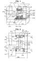
- FIG. 1 is a schematic bird's-eye view showing a transistor of a semiconductor device according to a first embodiment of the present invention.
- FIG. 2 is a schematic sectional view taken along the line A-A' in FIG. 1
- FIG. 3 is a top view of the transistor in FIG. 1 .
- FIG. 4, FIG. 5 and FIG. 6 are a schematic sectional view taken along the line B-B' in FIG. 2 , a schematic sectional view taken along the line C-C' in FIG. 2 , and a schematic sectional view taken along the line D-D' in FIG. 2 , respectively.
- the semiconductor device comprises: a first silicon pillar 830 formed on a first conductive-type semiconductor substrate 100 to have a cross-sectionally circular shape; a second silicon pillar 810 formed on the first silicon pillar 830 to have a cross-sectionally circular shape; a first insulator 310 surrounding a part of a surface of the second silicon pillar 810; a gate 210 surrounding the first insulator 310; and a third silicon pillar 820 formed on the second silicon pillar 810 to have a cross-sectionally circular shape.
- the second silicon pillar 810 includes a second conductive-type high-concentration impurity region 520 formed as a part of the second silicon pillar 810, and a second conductive-type high-concentration impurity region 530 formed as a part of the second silicon pillar 810.
- the semiconductor substrate 100 includes a second conductive-type high-concentration impurity region 510 formed as a part of the semiconductor substrate 100, and a silicide region (first silicide) 720 formed as a part of the high-concentration impurity region 510.
- the semiconductor substrate 100 also has an element isolation region 910 formed therein.
- the third silicon pillar 820 includes a second conductive-type high-concentration impurity region 540 formed as a part of the third silicon pillar 820, and a silicide region (second silicide) 710 is formed in the high-concentration impurity region 540.
- the first silicon pillar 830 includes a second conductive-type high-concentration impurity region 550 formed as a part of the first silicon pillar 830.
- the semiconductor device according to the first embodiment further comprises a contact 430 formed on the silicide region 720, a contact 420 formed on the silicide region 710, and a contact 410 formed on the gate 210.
- Each of a contact resistance R1 formed by the first silicon pillar 830 including the high-concentration impurity region 510 and the silicide region 720 formed in the first silicon pillar 830, and a contact resistance R2 formed by the third silicon pillar 820 including the high-concentration impurity region 540 and the silicide region 710 formed in the third silicon pillar 830, is a parasitic resistance.
- the contact resistances R1, R2 satisfy the following relational formulas (1-1), (1-2) with respect to a reference resistance Rs: R ⁇ 1 ⁇ Rs R ⁇ 2 ⁇ Rs
- the parasitic resistance R1 of the first silicon pillar 830, a contact resistivity ⁇ C , a sheet resistance ⁇ D of a first conductive-type impurity region, a circumferential length K1 of a cross-section of the first silicon pillar 830, and a height dimension L1 of the first silicon pillar 830 satisfy the following formula (1-4), wherein ⁇ is expressed as the formula (1-5).
- the parasitic resistance R2 of the third silicon pillar 820, a contact resistivity ⁇ C , a sheet resistance ⁇ D of a first conductive-type impurity region, a circumferential length K2 of a cross-section of the third silicon pillar 820, and a height dimension L2 of the third silicon pillar 820 satisfy the following formula (1-7). Further, given that the circumferential length K2 (cm) of the cross-section of the third silicon pillar 820 satisfies the following relational formula (1-8) with respect to a diameter W2 (cm) of the third silicon pillar 820.
- the contact resistivity ⁇ C and the sheet resistance ⁇ D are, respectively, 6.2e-8 ( ⁇ -cm 2 ) and 6.4e-3/W1 ( ⁇ /sq.)
- the current I (A) flowing between the contact 410 and the contact 430 in the above semiconductor device is 44 ( ⁇ A) when 0 (V) is applied to one of the contacts 410, 430 and 1 (V) is applied to a remaining one of the contacts 410, 430, while applying 1 (V) to the contact 420
- the reference resistance Rs is calculated as 2.3e-8 ( ⁇ ) according to the formula (1-3).
- each of the circumferential lengths of the third and first silicon pillars 820, 830 and the gate length are set, respectively, in the range of 8 nm to 100 ⁇ m, in the range of 8 nm to 100 ⁇ m and in the range of 6 nm to 10 ⁇ m.
- the contact resistivity ⁇ C and the sheet resistance ⁇ D are, respectively, 2.6 nm, 7e-9 ( ⁇ -cm 2 ) and 6.4e-3/W1 ( ⁇ /sq.), and the current I (A) flowing between the contact 410 and the contact 430 in the above semiconductor device is 11.4 ( ⁇ A) when 0 (V) is applied to one of the contacts 410, 430 and 1 (V) is applied to a remaining one of the contacts 410, 430, while applying 1 (V) to the contact 420, the reference resistance Rs is calculated as 9.0e-8 ( ⁇ ) according to the formula (1-3).
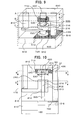
- FIG. 9 is a schematic bird's-eye view showing a transistor of a semiconductor device according to a second embodiment of the present invention.
- FIG. 10 is a schematic sectional view taken along the line A-A' in FIG. 9
- FIG. 11 is a top view of the transistor in FIG. 9 .
- FIG. 12 is a schematic sectional view taken along the line B-B' in FIG. 10
- FIG. 13 is a schematic sectional view taken along the line C-C' in FIG. 10 .
- the semiconductor device comprises a second silicon pillar 810 formed on a first conductive-type semiconductor substrate 100 to have a cross-sectionally circular shape, and a third silicon pillar 820 formed on the second silicon pillar 810 to have a cross-sectionally circular shape.
- the second silicon pillar 810 includes a second conductive-type high-concentration impurity region 520 formed as a part of the second silicon pillar 810, and a second conductive-type high-concentration impurity region 530 formed as a part of the second silicon pillar 810.
- the semiconductor substrate 100 includes a second conductive-type high-concentration impurity region 510 formed as a part of the semiconductor substrate 100, and a silicide region (first silicide) 720 formed as a part of the high-concentration impurity region 510.
- the semiconductor substrate 100 also has an element isolation region 910 formed therein.
- the third silicon pillar 820 includes a second conductive-type high-concentration impurity region 540 formed as a part of the third silicon pillar 820, and a silicide region (second silicide) 710 is formed in the high-concentration impurity region 540.
- the semiconductor device according to the second embodiment further comprises a contact 430 formed on the silicide region 720, a contact 420 formed on the silicide region 710, and a contact 410 formed on the gate 210.
- the structure in the second embodiment is designed to satisfy the following formula (2-1): R ⁇ 1 ⁇ ⁇ Rs , R ⁇ 1 ⁇ ⁇ R ⁇ 2
- the contact resistance R2 and a reference resistance Rs satisfy the following formula (2-2): R ⁇ 2 ⁇ Rs
- the contact resistance R of the third silicon pillar 820, a contact resistivity ⁇ C , a sheet resistance ⁇ D of a first conductive-type impurity region, a circumferential length K2 of a cross-section of the third silicon pillar 820, and a height dimension L2 of the third silicon pillar 820 satisfy the following formula (2-4), wherein ⁇ is expressed as the formula (2-5).
- the contact resistivity ⁇ C and the sheet resistance ⁇ D are, respectively, 6.2e-8 ( ⁇ -cm 2 ) and 6.4e-3/W1 ( ⁇ /sq.)
- the current I (A) flowing between the contact 410 and the contact 430 in the above semiconductor device is 44 ( ⁇ A) when 0 (V) is applied to one of the contacts 410, 430 and 1 (V) is applied to a remaining one of the contacts 410, 430, while applying 1 (V) to the contact 420
- the reference resistance Rs is calculated as 2.3e-8 ( ⁇ ) according to the formula (2-3).
- the circumferential length of the third silicon pillar 820 and the gate length are set, respectively, in the range of 8 nm to 100 ⁇ m, in the range of 8 nm to 100 ⁇ m and in the range of 6 nm to 10 ⁇ m.
- the contact resistivity ⁇ C and the sheet resistance ⁇ D are, respectively, 2.6 nm, 7e-9 ( ⁇ -cm 2 ) and 6.4e-3/W1 ( ⁇ /sq.), and the current I (A) flowing between the contact 410 and the contact 430 in the above semiconductor device is 11.4 ( ⁇ A) when 0 (V) is applied to one of the contacts 410, 430 and 1 (V) is applied to a remaining one of the contacts 410, 430, while applying 1 (V) to the contact 420, the reference resistance Rs is calculated as 9.0e-8 ( ⁇ ) according to the formula (2-3).
- the formula (2-7) is expressed as the following formula (2-10): ⁇ C ⁇ ⁇ K ⁇ 2 ⁇ coth L ⁇ 2 ⁇ ⁇ R s
- FIG. 15 is a schematic bird's-eye view showing a transistor of a semiconductor device according to a third embodiment of the present invention.
- FIG. 16 is a schematic sectional view taken along the line A-A' in FIG. 15
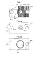
- FIG. 17 is a top view of the transistor in FIG. 14
- FIG. 18 is a schematic sectional view taken along the line B-B' in FIG. 15
- FIG. 19 is a schematic sectional view taken along the line C-C' in FIG. 15 .
- the semiconductor device comprises: a first silicon pillar 830 formed on a first conductive-type semiconductor substrate 100 to have a cross-sectionally circular shape; a second silicon pillar 810 formed on the first silicon pillar 830 to have a cross-sectionally circular shape; a first insulator 310 surrounding a part of a surface of the second silicon pillar 810; a gate 210 surrounding the first insulator 310; and a third silicon pillar 820 formed on the second silicon pillar 810 to have a cross-sectionally circular shape.
- the second silicon pillar 810 includes a second conductive-type high-concentration impurity region 520 formed as a part of the second silicon pillar 810, and a second conductive-type high-concentration impurity region 530 formed as a part of the second silicon pillar 810.
- the semiconductor substrate 100 includes a second conductive-type high-concentration impurity region 510 formed as a part of the semiconductor substrate 100, and a silicide region (first silicide) 720 formed as a part of the high-concentration impurity region 510.
- the semiconductor substrate 100 also has an element isolation region 910 formed therein.
- the third silicon pillar 820 includes a second conductive-type high-concentration impurity region 540 formed as a part of the third silicon pillar 820, and a silicide region (second silicide) 710 is formed in the high-concentration impurity region 540.
- the first silicon pillar 830 includes a second conductive-type high-concentration impurity region 550 formed as a part of the first silicon pillar 830.
- the semiconductor device according to the third embodiment further comprises a contact 430 formed on the silicide region 720, a contact 420 formed on the silicide region 710, and a contact 410 formed on the gate 210.
- the structure in the third embodiment is designed to satisfy the following formula (3-1): R ⁇ 2 ⁇ ⁇ Rs , R ⁇ 2 ⁇ ⁇ Rs
- the contact resistance R1 and a reference resistance Rs satisfy the following formula (3-2): R ⁇ 1 ⁇ Rs
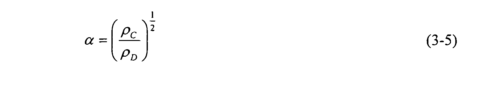
- the contact resistance R1 of the first silicon pillar 830, a contact resistivity ⁇ C , a sheet resistance ⁇ D of a first conductive-type impurity region, a circumferential length K1 of a cross-section of the first silicon pillar 830, and a height dimension L1 of the first silicon pillar 830 satisfy the following formula (3-4), wherein ⁇ is expressed as the formula (3-5).
- the formula (3-4) is assigned to the formula (3-1) to obtain the following conditional formula (3-7): ⁇ C ⁇ ⁇ K ⁇ 1 ⁇ coth L ⁇ 1 ⁇ ⁇ R s
- the contact resistivity ⁇ C and the sheet resistance ⁇ D are, respectively, 6.2e-8 ( ⁇ -cm 2 ) and 1.6e-3 ⁇ 4/W1 ( ⁇ /sq.)
- the current I (A) flowing between the contact 410 and the contact 430 in the above semiconductor device is 44 ( ⁇ A) when 0 (V) is applied to one of the contacts 410, 430 and 1 (V) is applied to a remaining one of the contacts 410, 430, while applying 1 (V) to the contact 420
- the reference resistance Rs is calculated as 2.3e-8 ( ⁇ ) according to the formula (3-3).
- the circumferential length of the first silicon pillar 830 and the gate length are set, respectively, in the range of 8 nm to 100 ⁇ m, in the range of 8 nm to 100 ⁇ m and in the range of 6 nm to 10 ⁇ m.
- each of the first silicide region 710 and the second silicide region 720 may be made of one selected from the group consisting of nickel (Ni) silicide, platinum (Pt) silicide, erbium (Er) silicide, ytterbium (Yb) silicide and a combination of two or more thereof.
- the present invention provides a semiconductor device which comprises: a first silicon pillar formed on a semiconductor substrate; a second silicon pillar formed on the first silicon pillar; a first insulator surrounding a part of a surface of the second silicon pillar; a gate surrounding the first insulator; a third silicon pillar formed on the second silicon pillar; a first silicide surrounding a part of a surface of the first silicon pillar; and a second silicide surrounding a part of a surface of the third silicon pillar, wherein each of a contact resistance formed by the first silicide and the first silicon pillar, and a contact resistance formed by the second silicide and the third silicon pillar, is less than a reference resistance of the semiconductor device.
- the present invention can provide a semiconductor device capable of solving problems of increase in power consumption and lowering in operation speed due to an increase in parasitic resistance of an SGT, to achieve high-speed SGT operation and low power consumption.
Landscapes
- Insulated Gate Type Field-Effect Transistor (AREA)
- Electrodes Of Semiconductors (AREA)
- Thin Film Transistor (AREA)
Abstract
Description
- The present invention relates to a semiconductor device, and more specifically to a semiconductor device having a surrounding gate transistor (SGT) which is a three-dimensional semiconductor.
- Through miniaturization of semiconductor devices using a planar transistor, the planar transistor is used in a wide range of fields, such as computers, communication devices, measurement devices, automatic control devices and domestic devices, as a low-power consumption, low-cost, high-throughput microprocessor, an ASIC, a microcomputer, and a low-cost, large-capacity memory. However, the planar transistor is two-dimensionally formed on a plane of a semiconductor substrate. Specifically, the planar transistor has a structure where a source, a gate and a drain thereof are arranged along a surface of a silicon substrate in a horizontal direction. In contrast, the SGT has a structure where a source, a gate and a drain thereof are arranged in a direction perpendicular to a surface of a silicon substrate while allowing the gate to surround a convex-shaped semiconductor layer (see, for example,
FIG. 20 in the following Non-Patent Document 1). Therefore, the SGT can largely reduce an occupancy area as compared with the planar transistor. However, in the SGT, along with miniaturization of ultra-large-scale integrated circuits (ULSI), a gate length becomes shorter to provide a lower channel resistance, whereas, as a silicon pillar becomes miniaturized, a diffusion-layer resistance and a contact resistance, i.e., a parasitic resistance, become larger to cause a reduction in drive current. Thus, in a miniaturized SGT device, it is essential to further reduce a parasitic resistance. - There has been known a technique of reducing a contact resistance as a parasitic resistance of source and drain regions to achieve a higher-speed operation of the device, as disclosed, for example, in the following
Patent Document 1.FIG. 21 shows an SGT structure disclosed in thePatent Document 1, which is intended to reduce the contact resistance. In an SGT, along with scaling down of a silicon pillar, a contact area between the silicon pillar and a contact to be connected to a top of the silicon pillar becomes smaller to cause an increase in contact resistance. Consequently, a drive current of the SGT is reduced. As measures against this problem, thePatent Document 1 discloses a structure for increasing the contact area between the silicon pillar and the contact so as to reduce the contact resistance. Specifically, the structure is configured to allow the contact to come into contact with not only a top surface of the silicon pillar but also a part of a side surface of the silicon pillar, so that the contact area between the silicon pillar and the contact is increased to reduce the contact resistance. - [Non-Patent Document 1] H.Takato et al., IEEE transaction on electron device, Vol. 38, No. 3, March 1991, pp 573-578
[Patent Document 1]JP 2007-123415A - As an SGT structure for reducing the contact resistance, the
Patent Document 1 proposes a structure where the contact area between the silicon pillar and the contact is set to become greater than an area of the top surface of the silicon pillar, to reduce the contact resistance. However, in order to actually achieve a higher-speed operation of an SGT constituting a ULSI, it is desirable that the contact resistance is less than a reference resistance of the SGT.
In view of the above circumstances, it is an object of the present invention to provide a semiconductor device capable of reducing a contact resistance as a parasitic resistance to solve the problem of lowering in operation speed of an SGT. - In order to achieve the above object, according to a first aspect of the present invention, there is provided a semiconductor device which comprises: a first silicon pillar formed on a semiconductor substrate; a second silicon pillar formed on the first silicon pillar; a first insulator surrounding a part of a surface of the second silicon pillar; a gate surrounding the first insulator; a third silicon pillar formed on the second silicon pillar; a first silicide surrounding a part of a surface of the first silicon pillar; and a second silicide surrounding a part of a surface of the third silicon pillar, wherein each of a contact resistance formed by the first silicide and the first silicon pillar, and a contact resistance formed by the second silicide and the third silicon pillar, is less than a reference resistance of the semiconductor device.
- According to a second aspect of the present invention, there is provided a semiconductor device which comprises: a second silicon pillar formed on a semiconductor substrate; a first insulator surrounding a part of a surface of the second silicon pillar; a gate surrounding the first insulator; a third silicon pillar formed on the second silicon pillar; and a second silicide surrounding a part of a surface of the third silicon pillar, wherein a contact resistance formed by the second silicide and the third silicon pillar is less than a reference resistance of the semiconductor device.
- According to a third aspect of the present invention, there is provided a semiconductor device which comprises: a first silicon pillar formed on a semiconductor substrate; a second silicon pillar formed on the first silicon pillar; a first insulator surrounding a part of a surface of the second silicon pillar; a gate surrounding the first insulator; and a first silicide surrounding a part of a surface of the first silicon pillar, wherein a contact resistance formed by the first silicide and the first silicon pillar is less than a reference resistance of the semiconductor device.
As above, the present invention makes it possible to reduce a parasitic resistance of a semiconductor device element to provide a semiconductor device having a high-speed, low-power consumption ULSI. -
-
FIG. 1 is a bird's-eye view showing a semiconductor device according to a first embodiment of the present invention. -
FIG. 2 is a sectional view of the semiconductor device, taken along the line A-A' inFIG. 1 . -
FIG. 3 is a top view of the semiconductor device inFIG. 1 . -
FIG. 4 is a sectional view of the semiconductor device, taken along the line B-B' inFIG. 2 . -
FIG. 5 is a sectional view of the semiconductor device, taken along the line C-C' inFIG. 2 . -
FIG. 6 is a sectional view of the semiconductor device, taken along the line D-D' inFIG. 2 . -
FIG. 7 is a graph showing a relationship between a diameter W1 and a length L1 of afirst silicon pillar 830 for satisfying a condition that a contact resistance formed by a silicide and thefirst silicon pillar 830 is less than a reference resistance in the semiconductor device inFIG. 1 . -
FIG. 8 is a graph showing a relationship between a diameter W2 and a length L2 of athird silicon pillar 820 for satisfying a condition that a contact resistance formed by a silicide and thethird silicon pillar 820 is less than a reference resistance in the semiconductor device inFIG. 1 . -
FIG. 9 is a bird's-eye view showing a semiconductor device according to a second embodiment of the present invention. -
FIG. 10 is a sectional view of the semiconductor device, taken along the line A-A' inFIG. 9 . -
FIG. 11 is a top view of the semiconductor device inFIG. 9 . -
FIG. 12 is a sectional view of the semiconductor device, taken along the line B-B' inFIG. 10 . -
FIG. 13 is a sectional view of the semiconductor device, taken along the line C-C' inFIG. 10 . -
FIG. 14 is a graph showing a relationship between a diameter W2 and a length L2 of athird silicon pillar 820 for satisfying a condition that a contact resistance formed by a silicide and thethird silicon pillar 820 is less than a reference resistance in the semiconductor device inFIG. 9 . -
FIG. 15 is a bird's-eye view showing a semiconductor device according to a third embodiment of the present invention. -
FIG. 16 is a sectional view of the semiconductor device, taken along the line A-A' inFIG. 15 . -
FIG. 17 is a top view of the semiconductor device inFIG. 15 . -
FIG. 18 is a sectional view of the semiconductor device, taken along the line B-B' inFIG. 16 . -
FIG. 19 is a sectional view of the semiconductor device, taken along the line C-C' inFIG. 16 . -
FIG. 20 is a graph showing a relationship between a diameter W1 and a length L1 of afirst silicon pillar 830 for satisfying a condition that a contact resistance formed by a silicide and thefirst silicon pillar 830 is less than a reference resistance in the semiconductor device inFIG. 1 . -
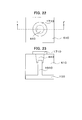
FIG. 21 is a bird's-eye view showing one example of a conventional SGT. -
FIG. 22 is a top view of the conventional SGT. -
FIG. 23 is a sectional view of the conventional SGT, taken along the line I-I' inFIG. 22 . - With reference to the drawings, a semiconductor device of the present invention will now be specifically described.
-
FIG. 1 is a schematic bird's-eye view showing a transistor of a semiconductor device according to a first embodiment of the present invention.FIG. 2 is a schematic sectional view taken along the line A-A' inFIG. 1 , andFIG. 3 is a top view of the transistor inFIG. 1 .FIG. 4, FIG. 5 and FIG. 6 are a schematic sectional view taken along the line B-B' inFIG. 2 , a schematic sectional view taken along the line C-C' inFIG. 2 , and a schematic sectional view taken along the line D-D' inFIG. 2 , respectively. The semiconductor device according to the first embodiment comprises: afirst silicon pillar 830 formed on a first conductive-type semiconductor substrate 100 to have a cross-sectionally circular shape; asecond silicon pillar 810 formed on thefirst silicon pillar 830 to have a cross-sectionally circular shape; afirst insulator 310 surrounding a part of a surface of thesecond silicon pillar 810; agate 210 surrounding thefirst insulator 310; and athird silicon pillar 820 formed on thesecond silicon pillar 810 to have a cross-sectionally circular shape. - The
second silicon pillar 810 includes a second conductive-type high-concentration impurity region 520 formed as a part of thesecond silicon pillar 810, and a second conductive-type high-concentration impurity region 530 formed as a part of thesecond silicon pillar 810.
Thesemiconductor substrate 100 includes a second conductive-type high-concentration impurity region 510 formed as a part of thesemiconductor substrate 100, and a silicide region (first silicide) 720 formed as a part of the high-concentration impurity region 510. Thesemiconductor substrate 100 also has anelement isolation region 910 formed therein. - The
third silicon pillar 820 includes a second conductive-type high-concentration impurity region 540 formed as a part of thethird silicon pillar 820, and a silicide region (second silicide) 710 is formed in the high-concentration impurity region 540.
Thefirst silicon pillar 830 includes a second conductive-type high-concentration impurity region 550 formed as a part of thefirst silicon pillar 830.
The semiconductor device according to the first embodiment further comprises acontact 430 formed on thesilicide region 720, acontact 420 formed on thesilicide region 710, and acontact 410 formed on thegate 210. - Each of a contact resistance R1 formed by the
first silicon pillar 830 including the high-concentration impurity region 510 and thesilicide region 720 formed in thefirst silicon pillar 830, and a contact resistance R2 formed by thethird silicon pillar 820 including the high-concentration impurity region 540 and thesilicide region 710 formed in thethird silicon pillar 830, is a parasitic resistance. In order to reduce the parasitic resistance, it is preferable that the contact resistances R1, R2 satisfy the following relational formulas (1-1), (1-2) with respect to a reference resistance Rs:

- The reference resistance Rs is calculated according to the following formula (1-3) based on a current I (A) which flows between the
contact 410 and thecontact 430 in the above semiconductor device when 0 (V) is applied to one of thecontacts contacts contact 420, under a condition that the contact resistance R1 = 0 and the contact resistance R2 = 0:
- Specifically, when a length of the
gate 210, a film thickness of the gate oxide layer, and a diameter of thesecond silicon pillar 810, are, respectively, 20 nm, 1 nm, and 10 nm, the parasitic resistance R1 of thefirst silicon pillar 830, a contact resistivity ρC, a sheet resistance ρD of a first conductive-type impurity region, a circumferential length K1 of a cross-section of thefirst silicon pillar 830, and a height dimension L1 of thefirst silicon pillar 830, satisfy the following formula (1-4), wherein α is expressed as the formula (1-5). Further, given that the circumferential length K1 (cm) of the cross-section of thefirst silicon pillar 830 satisfies the following relational formula (1-6) with respect to a diameter W1 (cm) of thefirst silicon pillar 830.


- The parasitic resistance R2 of the
third silicon pillar 820, a contact resistivity ρC, a sheet resistance ρD of a first conductive-type impurity region, a circumferential length K2 of a cross-section of thethird silicon pillar 820, and a height dimension L2 of thethird silicon pillar 820, satisfy the following formula (1-7). Further, given that the circumferential length K2 (cm) of the cross-section of thethird silicon pillar 820 satisfies the following relational formula (1-8) with respect to a diameter W2 (cm) of thethird silicon pillar 820.

- The formula (1-4) is assigned to the formula (1-1), and the formula (1-7) is assigned to the formula (1-2), to obtain the following conditional formulas (1-9), (1-10):


- As one example, given that the contact resistivity ρC and the sheet resistance ρD are, respectively, 6.2e-8 (Ω-cm2) and 6.4e-3/W1 (Ω/sq.), and the current I (A) flowing between the
contact 410 and thecontact 430 in the above semiconductor device is 44 (µA) when 0 (V) is applied to one of thecontacts contacts contact 420, the reference resistance Rs is calculated as 2.3e-8 (Ω) according to the formula (1-3). These values are assigned to the formulas (1-9), (1-10) to obtain the following relational formula (1-11) between the height dimension L1 of thefirst silicon pillar 830 and the circumferential length K1 of the cross-section of thefirst silicon pillar 830, and the following relational formula (1-12) between the height dimension L2 (cm) of thethird silicon pillar 820 and the circumferential length K2 (cm) of the cross-section of the third silicon pillar 820:

- If these conditional formulas (1-11), (1-12) are satisfied, the formulas (1-1) are satisfied. Thus, the following formulas (1-13), (1-14) are obtained (see
FIGS. 7 and 8 ):

- As another example, given that a circumferential length of the
second silicon pillar 810, each of the circumferential lengths of the third andfirst silicon pillars second silicon pillar 810, the contact resistivity ρC and the sheet resistance ρD are, respectively, 2.6 nm, 7e-9 (Ω-cm2) and 6.4e-3/W1 (Ω/sq.), and the current I (A) flowing between thecontact 410 and thecontact 430 in the above semiconductor device is 11.4 (µA) when 0 (V) is applied to one of thecontacts contacts contact 420, the reference resistance Rs is calculated as 9.0e-8 (Ω) according to the formula (1-3). These values are assigned to the formulas (1-8), (1-9) to obtain the following formulas (1-15), (1-16):

- If these conditional formulas (1-15), (1-16) are satisfied, the formulas (1-1), (1-2) are satisfied. Thus, the following formulas (1-17), (1-18) are obtained:


-
FIG. 9 is a schematic bird's-eye view showing a transistor of a semiconductor device according to a second embodiment of the present invention.FIG. 10 is a schematic sectional view taken along the line A-A' inFIG. 9 , andFIG. 11 is a top view of the transistor inFIG. 9 .FIG. 12 is a schematic sectional view taken along the line B-B' inFIG. 10 , andFIG. 13 is a schematic sectional view taken along the line C-C' inFIG. 10 . The semiconductor device according to the second embodiment comprises asecond silicon pillar 810 formed on a first conductive-type semiconductor substrate 100 to have a cross-sectionally circular shape, and athird silicon pillar 820 formed on thesecond silicon pillar 810 to have a cross-sectionally circular shape. - A part of a surface of the
second silicon pillar 810 is surrounded by afirst insulator 310, and thefirst insulator 310 is surrounded by agate 210. Thesecond silicon pillar 810 includes a second conductive-type high-concentration impurity region 520 formed as a part of thesecond silicon pillar 810, and a second conductive-type high-concentration impurity region 530 formed as a part of thesecond silicon pillar 810.
Thesemiconductor substrate 100 includes a second conductive-type high-concentration impurity region 510 formed as a part of thesemiconductor substrate 100, and a silicide region (first silicide) 720 formed as a part of the high-concentration impurity region 510. Thesemiconductor substrate 100 also has anelement isolation region 910 formed therein. - The
third silicon pillar 820 includes a second conductive-type high-concentration impurity region 540 formed as a part of thethird silicon pillar 820, and a silicide region (second silicide) 710 is formed in the high-concentration impurity region 540.
The semiconductor device according to the second embodiment further comprises acontact 430 formed on thesilicide region 720, acontact 420 formed on thesilicide region 710, and acontact 410 formed on thegate 210. - Differently from the first embodiment, on an assumption that a contact resistance R1 formed by the
semiconductor substrate 100 including the high-concentration impurity region 510 and thesilicide region 720 formed in thesemiconductor substrate 100 is ignorable, the structure in the second embodiment is designed to satisfy the following formula (2-1):
- In this case, in order to reduce a contact resistance or parasitic resistance R2 formed by the
third silicon pillar 820 including the high-concentration impurity region 540 and thesilicide region 710 formed in thethird silicon pillar 830, it is preferable that the contact resistance R2 and a reference resistance Rs satisfy the following formula (2-2):
- The reference resistance Rs is calculated according to the following formula (2-3) based on a current I (A) which flows between the
contact 410 and thecontact 430 in the above semiconductor device when 0 (V) is applied to one of thecontacts contacts contact 420, under a condition that the contact resistance R1 = 0 and the contact resistance R2 = 0:
- Specifically, when a length of the
gate 210, a film thickness of the gate oxide layer, and a diameter of thesecond silicon pillar 810, are, respectively, 20 nm, 1 nm, and 10 nm, the contact resistance R of thethird silicon pillar 820, a contact resistivity ρC, a sheet resistance ρD of a first conductive-type impurity region, a circumferential length K2 of a cross-section of thethird silicon pillar 820, and a height dimension L2 of thethird silicon pillar 820, satisfy the following formula (2-4), wherein α is expressed as the formula (2-5). Further, given that the circumferential length K2 (cm) of the cross-section of thethird silicon pillar 820 satisfies the following relational formula (2-6) with respect to a diameter W2 (cm) of thethird silicon pillar 820.


- The formula (2-4) is assigned to the formula (2-1) to obtain the following conditional formulas (2-7):

- As one example, given that the contact resistivity ρC and the sheet resistance ρD are, respectively, 6.2e-8 (Ω-cm2) and 6.4e-3/W1 (Ω/sq.), and the current I (A) flowing between the
contact 410 and thecontact 430 in the above semiconductor device is 44 (µA) when 0 (V) is applied to one of thecontacts contacts contact 420, the reference resistance Rs is calculated as 2.3e-8 (Ω) according to the formula (2-3). These values are assigned to the formula (2-7) to obtain the following relational formula (2-8) between the height dimension L2 (cm) of thethird silicon pillar 820 and the circumferential length K2 (cm) of the cross-section of the third silicon pillar 820:
- If the conditional formula (2-8) is satisfied, the formula (2-1) is satisfied. Thus, the following formula (2-9) is obtained (see
FIG. 14 ):
- As another example, given that a circumferential length of each of the second and
first silicon pillars third silicon pillar 820 and the gate length are set, respectively, in the range of 8 nm to 100 µm, in the range of 8 nm to 100 µm and in the range of 6 nm to 10 µm. Further, given that the diameter of thesecond silicon pillar 810, the contact resistivity ρC and the sheet resistance ρD are, respectively, 2.6 nm, 7e-9 (Ω-cm2) and 6.4e-3/W1 (Ω/sq.), and the current I (A) flowing between thecontact 410 and thecontact 430 in the above semiconductor device is 11.4 (µA) when 0 (V) is applied to one of thecontacts contacts contact 420, the reference resistance Rs is calculated as 9.0e-8 (Ω) according to the formula (2-3). Thus, the formula (2-7) is expressed as the following formula (2-10):
- The above values are assigned to the formula (2-10) to obtain the following formula (2-11):

- If the conditional formula (2-11) is satisfied, the formula (2-1) is satisfied. Thus, the following formula (2-12) is obtained:

-
FIG. 15 is a schematic bird's-eye view showing a transistor of a semiconductor device according to a third embodiment of the present invention.FIG. 16 is a schematic sectional view taken along the line A-A' inFIG. 15 , andFIG. 17 is a top view of the transistor inFIG. 14 FIG. 18 is a schematic sectional view taken along the line B-B' inFIG. 15 andFIG. 19 is a schematic sectional view taken along the line C-C' inFIG. 15 . The semiconductor device according to the third embodiment comprises: afirst silicon pillar 830 formed on a first conductive-type semiconductor substrate 100 to have a cross-sectionally circular shape; asecond silicon pillar 810 formed on thefirst silicon pillar 830 to have a cross-sectionally circular shape; afirst insulator 310 surrounding a part of a surface of thesecond silicon pillar 810; agate 210 surrounding thefirst insulator 310; and athird silicon pillar 820 formed on thesecond silicon pillar 810 to have a cross-sectionally circular shape. - The
second silicon pillar 810 includes a second conductive-type high-concentration impurity region 520 formed as a part of thesecond silicon pillar 810, and a second conductive-type high-concentration impurity region 530 formed as a part of thesecond silicon pillar 810.
Thesemiconductor substrate 100 includes a second conductive-type high-concentration impurity region 510 formed as a part of thesemiconductor substrate 100, and a silicide region (first silicide) 720 formed as a part of the high-concentration impurity region 510. Thesemiconductor substrate 100 also has anelement isolation region 910 formed therein. - The
third silicon pillar 820 includes a second conductive-type high-concentration impurity region 540 formed as a part of thethird silicon pillar 820, and a silicide region (second silicide) 710 is formed in the high-concentration impurity region 540.
Thefirst silicon pillar 830 includes a second conductive-type high-concentration impurity region 550 formed as a part of thefirst silicon pillar 830.
The semiconductor device according to the third embodiment further comprises acontact 430 formed on thesilicide region 720, acontact 420 formed on thesilicide region 710, and acontact 410 formed on thegate 210. - Differently from the first embodiment, on an assumption that a contact resistance R2 formed by the
third silicon pillar 820 including the high-concentration impurity region 540 and thesilicide region 710 formed in thethird silicon pillar 830 is ignorable, the structure in the third embodiment is designed to satisfy the following formula (3-1):
- In this case, in order to reduce a contact resistance or parasitic resistance R1 formed by the
first silicon pillar 830 including the high-concentration impurity region 510 and thesilicide region 720 formed in thefirst silicon pillar 830, it is preferable that the contact resistance R1 and a reference resistance Rs satisfy the following formula (3-2):
- The reference resistance Rs is calculated according to the following formula (3-3) based on a current I (A) which flows between the
contact 410 and thecontact 430 in the above semiconductor device when 0 (V) is applied to one of thecontacts contacts contact 420, under a condition that the contact resistance R1 = 0 and the contact resistance R2 = 0:
- Specifically, when a length of the
gate 210, a film thickness of the gate oxide layer, and a diameter of thesecond silicon pillar 810, are, respectively, 20 nm, 1 nm, and 10 nm, the contact resistance R1 of thefirst silicon pillar 830, a contact resistivity ρC, a sheet resistance ρD of a first conductive-type impurity region, a circumferential length K1 of a cross-section of thefirst silicon pillar 830, and a height dimension L1 of thefirst silicon pillar 830, satisfy the following formula (3-4), wherein α is expressed as the formula (3-5). Further, given that the circumferential length K1 (cm) of the cross-section of thefirst silicon pillar 830 satisfies the following relational formula (3-6) with respect to a diameter W1 (cm) of thefirst silicon pillar 830.

- The formula (3-4) is assigned to the formula (3-1) to obtain the following conditional formula (3-7):

- As one example, given that the contact resistivity ρC and the sheet resistance ρD are, respectively, 6.2e-8 (Ω-cm2) and 1.6e-3 × 4/W1 (Ω/sq.), and the current I (A) flowing between the
contact 410 and thecontact 430 in the above semiconductor device is 44 (µA) when 0 (V) is applied to one of thecontacts contacts contact 420, the reference resistance Rs is calculated as 2.3e-8 (Ω) according to the formula (3-3). These values are assigned to the formula (3-7) to obtain the following relational formula (3-8) between the height dimension L1 of thefirst silicon pillar 830 and the circumferential length K1 of the cross-section of the first silicon pillar 830:
- If the conditional formula (3-8) is satisfied, the formula (3-1) is satisfied. Thus, the following formula (3-9) is obtained (see
FIG. 20 ):
- As another example, given that a circumferential length of each of the second and
third silicon pillars first silicon pillar 830 and the gate length are set, respectively, in the range of 8 nm to 100 µm, in the range of 8 nm to 100 µm and in the range of 6 nm to 10 µm. Further, given that the diameter of thesecond silicon pillar 810, the contact resistivity ρC and the sheet resistance ρD are, respectively, 2.6 nm, 7e-9 (Ω-cm2) and 1.6e-3 × 4/W1 (Ω/sq.), and the current I (A) flowing between thecontact 410 and thecontact 430 in the above semiconductor device is 11.4 (µA) when 0 (V) is applied to one of thecontacts contacts contact 420, the reference resistance Rs is calculated as 9e-8 (Ω) according to the formula (3-3). Further, given that L1 = L2 and K1 = K2, the following formula (3-10) is obtained:
- The above values are assigned to the formula (3-10) to obtain the following formula (3-11):

- If the conditional formula (3-11) is satisfied, the formula (3-1) is satisfied. Thus, the following formula (3-12) is obtained:

In the first to third embodiments, each of thefirst silicide region 710 and thesecond silicide region 720 may be made of one selected from the group consisting of nickel (Ni) silicide, platinum (Pt) silicide, erbium (Er) silicide, ytterbium (Yb) silicide and a combination of two or more thereof. - As mentioned above, the present invention provides a semiconductor device which comprises: a first silicon pillar formed on a semiconductor substrate; a second silicon pillar formed on the first silicon pillar; a first insulator surrounding a part of a surface of the second silicon pillar; a gate surrounding the first insulator; a third silicon pillar formed on the second silicon pillar; a first silicide surrounding a part of a surface of the first silicon pillar; and a second silicide surrounding a part of a surface of the third silicon pillar, wherein each of a contact resistance formed by the first silicide and the first silicon pillar, and a contact resistance formed by the second silicide and the third silicon pillar, is less than a reference resistance of the semiconductor device.
The present invention can provide a semiconductor device capable of solving problems of increase in power consumption and lowering in operation speed due to an increase in parasitic resistance of an SGT, to achieve high-speed SGT operation and low power consumption. -
- 100, 110:
- semiconductor substrate
- 210:
- gate
- 310:
- gate insulating layer
- 410, 420, 430, 440:
- contact
- 510, 520, 530, 540:
- high-concentration impurity diffusion layer
- 610:
- inter-layer insulating film
- 710, 720:
- silicide
- 810, 820:
- silicon pillar
- 910:
- element-isolation insulating film
- 1010:
- high-resistance region
- 1110:
- sidewall oxide film
- 1210:
- contact-hole etching stopper layer
- 1310:
- source
- 1410:
- drain
- 1610:
- channel region
- 1710:
- metal line portion
- 1810:
- Al
- 1910:
- convex-shaped semiconductor
Claims (8)
- A semiconductor device comprising: a first silicon pillar formed on a semiconductor substrate; a second silicon pillar formed on the first silicon pillar; a first insulator surrounding a part of a surface of the second silicon pillar; a gate surrounding the first insulator; a third silicon pillar formed on the second silicon pillar; a first silicide surrounding a part of a surface of the first silicon pillar; and a second silicide surrounding a part of a surface of the third silicon pillar, wherein each of a contact resistance formed by the first silicide and the first silicon pillar, and a contact resistance formed by the second silicide and the third silicon pillar, is less than a reference resistance of the semiconductor device.
- A semiconductor device comprising: a second silicon pillar formed on a semiconductor substrate; a first insulator surrounding a part of a surface of the second silicon pillar; a gate surrounding the first insulator; a third silicon pillar formed on the second silicon pillar; and a second silicide surrounding a part of a surface of the third silicon pillar, wherein a contact resistance formed by the second silicide and the third silicon pillar is less than a reference resistance of the semiconductor device.
- A semiconductor device comprising: a first silicon pillar formed on a semiconductor substrate; a second silicon pillar formed on the first silicon pillar; a first insulator surrounding a part of a surface of the second silicon pillar; a gate surrounding the first insulator; and a first silicide surrounding a part of a surface of the first silicon pillar, wherein a contact resistance formed by the first silicide and the first silicon pillar is less than a reference resistance of the semiconductor device.
- A semiconductor device comprising: a first silicon pillar formed on a semiconductor substrate; a second silicon pillar formed on the first silicon pillar; a first insulator surrounding a part of a surface of the second silicon pillar; a gate surrounding the first insulator; a third silicon pillar formed on the second silicon pillar; a first silicide surrounding a part of a surface of the
first silicon pillar; and a second silicide surrounding a part of a surface of the third silicon pillar, wherein a diameter W1 (cm) and a height dimension L1 (cm) of the first silicon pillar, and a diameter W2 (cm) and a height dimension L2 (cm) of the third silicon pillar, satisfy the following relations:
- A semiconductor device comprising: a second silicon pillar formed on a semiconductor substrate; a first insulator surrounding a part of a surface of the second silicon pillar; a gate surrounding the first insulator; a third silicon pillar formed on the second silicon pillar; and a second silicide surrounding a part of a surface of the third silicon pillar, wherein a diameter W2 (cm) and a height dimension L2 (cm) of the third silicon pillar satisfy the following relation:

- A semiconductor device comprising: a first silicon pillar formed on a semiconductor substrate; a second silicon pillar formed on the first silicon pillar; a first insulator surrounding a part of a surface of the second silicon pillar; a gate surrounding the first insulator; and a first silicide surrounding a part of a surface of the first silicon pillar, wherein a diameter W1 (cm) and a height dimension L1 (cm) of the first silicon pillar satisfy the following relation:

- The semiconductor device as defined in any one of claims 1 to 6, wherein each of the first silicide and the second silicide is one selected from the group consisting of nickel (Ni) silicide, platinum (Pt) silicide, erbium (Er) silicide, ytterbium (Yb) silicide and a combination of two or
, and
- The semiconductor device as defined in any one of claims 1 to 7, wherein each of the first silicon pillar and the third silicon pillar includes a high-concentration impurity region.
Applications Claiming Priority (1)
| Application Number | Priority Date | Filing Date | Title |
|---|---|---|---|
| PCT/JP2007/073935 WO2009075031A1 (en) | 2007-12-12 | 2007-12-12 | Semiconductor device |
Publications (2)
| Publication Number | Publication Date |
|---|---|
| EP2221858A1 true EP2221858A1 (en) | 2010-08-25 |
| EP2221858A4 EP2221858A4 (en) | 2012-10-17 |
Family
ID=40755288
Family Applications (1)
| Application Number | Title | Priority Date | Filing Date |
|---|---|---|---|
| EP07850486A Withdrawn EP2221858A4 (en) | 2007-12-12 | 2007-12-12 | Semiconductor device |
Country Status (5)
| Country | Link |
|---|---|
| EP (1) | EP2221858A4 (en) |
| JP (1) | JPWO2009075031A1 (en) |
| KR (1) | KR101128244B1 (en) |
| CN (1) | CN101897008B (en) |
| WO (1) | WO2009075031A1 (en) |
Families Citing this family (6)
| Publication number | Priority date | Publication date | Assignee | Title |
|---|---|---|---|---|
| JP5973665B2 (en) * | 2013-06-13 | 2016-08-23 | ユニサンティス エレクトロニクス シンガポール プライベート リミテッドUnisantis Electronics Singapore Pte Ltd. | Semiconductor device having SGT and manufacturing method thereof |
| WO2017104066A1 (en) * | 2015-12-18 | 2017-06-22 | ユニサンティス エレクトロニクス シンガポール プライベート リミテッド | Sgt-including semiconductor device and method for producing same |
| US12414285B2 (en) | 2022-04-26 | 2025-09-09 | Changxin Memory Technologies, Inc. | Semiconductor structure and manufacturing method thereof |
| US12369295B2 (en) | 2022-04-26 | 2025-07-22 | Changxin Memory Technologies, Inc. | Semiconductor structure and manufacturing method thereof |
| CN117015232A (en) * | 2022-04-26 | 2023-11-07 | 长鑫存储技术有限公司 | Semiconductor structure and preparation method thereof, semiconductor device |
| US12342524B2 (en) | 2022-04-26 | 2025-06-24 | Changxin Memory Technologies, Inc. | Method for fabricating semiconductor device and semiconductor device |
Family Cites Families (12)
| Publication number | Priority date | Publication date | Assignee | Title |
|---|---|---|---|---|
| JPH01232755A (en) * | 1988-03-11 | 1989-09-18 | Fujitsu Ltd | Semiconductor device and manufacture thereof |
| JP2804539B2 (en) * | 1989-09-28 | 1998-09-30 | 沖電気工業株式会社 | Semiconductor device and manufacturing method thereof |
| JPH06310730A (en) * | 1993-04-21 | 1994-11-04 | Hitachi Ltd | Semiconductor integrated circuit device and fabrication thereof |
| JPH08227997A (en) * | 1995-02-20 | 1996-09-03 | Hitachi Ltd | Semiconductor device and manufacturing method thereof |
| DE19711482C2 (en) * | 1997-03-19 | 1999-01-07 | Siemens Ag | Method of manufacturing a vertical MOS transistor |
| JP4078721B2 (en) * | 1998-08-24 | 2008-04-23 | ソニー株式会社 | Semiconductor device and manufacturing method thereof |
| JP2003101012A (en) * | 2001-09-25 | 2003-04-04 | Sony Corp | Semiconductor device and method of manufacturing the same |
| US7378702B2 (en) * | 2004-06-21 | 2008-05-27 | Sang-Yun Lee | Vertical memory device structures |
| JP2006261421A (en) * | 2005-03-17 | 2006-09-28 | Toshiba Corp | Semiconductor device |
| JP5017795B2 (en) * | 2005-04-13 | 2012-09-05 | 日本電気株式会社 | Method for manufacturing field effect transistor |
| JP2007123415A (en) | 2005-10-26 | 2007-05-17 | Sharp Corp | Semiconductor device and manufacturing method thereof |
| WO2009072192A1 (en) * | 2007-12-05 | 2009-06-11 | Unisantis Electronics (Japan) Ltd. | Semiconductor device |
-
2007
- 2007-12-12 WO PCT/JP2007/073935 patent/WO2009075031A1/en not_active Ceased
- 2007-12-12 CN CN2007801019041A patent/CN101897008B/en not_active Expired - Fee Related
- 2007-12-12 EP EP07850486A patent/EP2221858A4/en not_active Withdrawn
- 2007-12-12 JP JP2009545319A patent/JPWO2009075031A1/en not_active Abandoned
- 2007-12-12 KR KR1020107014590A patent/KR101128244B1/en not_active Expired - Fee Related
Also Published As
| Publication number | Publication date |
|---|---|
| CN101897008B (en) | 2012-03-28 |
| CN101897008A (en) | 2010-11-24 |
| KR20100093582A (en) | 2010-08-25 |
| KR101128244B1 (en) | 2012-03-23 |
| JPWO2009075031A1 (en) | 2011-04-28 |
| EP2221858A4 (en) | 2012-10-17 |
| WO2009075031A1 (en) | 2009-06-18 |
Similar Documents
| Publication | Publication Date | Title |
|---|---|---|
| US20100187601A1 (en) | Semiconductor device | |
| US8502303B2 (en) | Semiconductor device | |
| US9837498B2 (en) | Stripe-shaped electrode structure including a main portion with a field electrode and an end portion terminating the electrode structure | |
| US8598669B2 (en) | Semiconductor device, and its manufacturing method | |
| US7514749B2 (en) | Semiconductor device and a method of manufacturing the same | |
| US9034755B2 (en) | Method of epitaxially forming contact structures for semiconductor transistors | |
| WO2012108165A1 (en) | Silicon carbide semiconductor device | |
| US20090140327A1 (en) | Semiconductor device and manufacturing method of the same | |
| US20160300945A1 (en) | Semiconductor Device with Cell Trench Structures and a Contact Structure | |
| KR101332590B1 (en) | Power semiconductor device having improved performance and method | |
| US8058703B2 (en) | Semiconductor transistor device and method of manufacturing the same | |
| US20140339650A1 (en) | Transistors having features which preclude straight-line lateral conductive paths from a channel reqion to a source/drain reqion | |
| CN118969846A (en) | Method for manufacturing a metal oxide semiconductor field effect transistor and a metal oxide semiconductor field effect transistor | |
| CN101897008B (en) | Semiconductor device | |
| US7859049B2 (en) | Semiconductor device | |
| CN102263107A (en) | A kind of semiconductor power device and its manufacturing method | |
| CN101740618B (en) | Metal-semiconductor field effect transistor | |
| US20130181288A1 (en) | Semiconductor device and method for manufacturing semiconductor device | |
| JP2008103378A (en) | Semiconductor device and manufacturing method thereof | |
| CN101740388B (en) | Method for manufacturing metal-semiconductor field effect transistor | |
| US20040222483A1 (en) | MOS power device with high integration density and manufacturing process thereof | |
| JP2011029564A (en) | Method for manufacturing semiconductor device and semiconductor device | |
| EP1703567A2 (en) | Insulated gate field-effect transistor and method of making the same | |
| CN102386225B (en) | Lateral double-diffused metal oxide semiconductor device and manufacturing method thereof |
Legal Events
| Date | Code | Title | Description |
|---|---|---|---|
| PUAI | Public reference made under article 153(3) epc to a published international application that has entered the european phase |
Free format text: ORIGINAL CODE: 0009012 |
|
| 17P | Request for examination filed |
Effective date: 20100511 |
|
| AK | Designated contracting states |
Kind code of ref document: A1 Designated state(s): AT BE BG CH CY CZ DE DK EE ES FI FR GB GR HU IE IS IT LI LT LU LV MC MT NL PL PT RO SE SI SK TR |
|
| AX | Request for extension of the european patent |
Extension state: AL BA HR MK RS |
|
| DAX | Request for extension of the european patent (deleted) | ||
| RAP1 | Party data changed (applicant data changed or rights of an application transferred) |
Owner name: UNISANTIS ELECTRONICS SINGAPORE PTE. LTD. |
|
| A4 | Supplementary search report drawn up and despatched |
Effective date: 20120919 |
|
| RIC1 | Information provided on ipc code assigned before grant |
Ipc: H01L 21/28 20060101ALI20120912BHEP Ipc: H01L 29/78 20060101ALI20120912BHEP Ipc: H01L 21/336 20060101AFI20120912BHEP Ipc: H01L 29/45 20060101ALI20120912BHEP |
|
| RAP1 | Party data changed (applicant data changed or rights of an application transferred) |
Owner name: UNISANTIS ELECTRONICS SINGAPORE PTE. LTD. |
|
| STAA | Information on the status of an ep patent application or granted ep patent |
Free format text: STATUS: THE APPLICATION IS DEEMED TO BE WITHDRAWN |
|
| 18D | Application deemed to be withdrawn |
Effective date: 20130419 |