EP2218169B2 - Wechselstrom-gleichstrom-aufwärtswandler ohne brücke - Google Patents
Wechselstrom-gleichstrom-aufwärtswandler ohne brücke Download PDFInfo
- Publication number
- EP2218169B2 EP2218169B2 EP08844429.4A EP08844429A EP2218169B2 EP 2218169 B2 EP2218169 B2 EP 2218169B2 EP 08844429 A EP08844429 A EP 08844429A EP 2218169 B2 EP2218169 B2 EP 2218169B2
- Authority
- EP
- European Patent Office
- Prior art keywords
- boost
- diode
- output terminal
- capacitor
- node
- Prior art date
- Legal status (The legal status is an assumption and is not a legal conclusion. Google has not performed a legal analysis and makes no representation as to the accuracy of the status listed.)
- Not-in-force
Links
- 239000003990 capacitor Substances 0.000 claims abstract description 41
- 230000006641 stabilisation Effects 0.000 claims abstract description 18
- 238000011105 stabilization Methods 0.000 claims abstract description 6
- 238000004088 simulation Methods 0.000 description 4
- 230000001965 increasing effect Effects 0.000 description 3
- 230000000903 blocking effect Effects 0.000 description 2
- 238000005259 measurement Methods 0.000 description 2
- UXUFTKZYJYGMGO-CMCWBKRRSA-N (2s,3s,4r,5r)-5-[6-amino-2-[2-[4-[3-(2-aminoethylamino)-3-oxopropyl]phenyl]ethylamino]purin-9-yl]-n-ethyl-3,4-dihydroxyoxolane-2-carboxamide Chemical compound O[C@@H]1[C@H](O)[C@@H](C(=O)NCC)O[C@H]1N1C2=NC(NCCC=3C=CC(CCC(=O)NCCN)=CC=3)=NC(N)=C2N=C1 UXUFTKZYJYGMGO-CMCWBKRRSA-N 0.000 description 1
- 238000013459 approach Methods 0.000 description 1
- 238000004891 communication Methods 0.000 description 1
- 238000011161 development Methods 0.000 description 1
- 230000000694 effects Effects 0.000 description 1
- 230000007613 environmental effect Effects 0.000 description 1
- 238000011156 evaluation Methods 0.000 description 1
- 230000001939 inductive effect Effects 0.000 description 1
- 238000000034 method Methods 0.000 description 1
- 238000012986 modification Methods 0.000 description 1
- 230000004048 modification Effects 0.000 description 1
- 230000001629 suppression Effects 0.000 description 1
- 238000012360 testing method Methods 0.000 description 1
Images



Classifications
-
- H—ELECTRICITY
- H02—GENERATION; CONVERSION OR DISTRIBUTION OF ELECTRIC POWER
- H02H—EMERGENCY PROTECTIVE CIRCUIT ARRANGEMENTS
- H02H7/00—Emergency protective circuit arrangements specially adapted for specific types of electric machines or apparatus or for sectionalised protection of cable or line systems, and effecting automatic switching in the event of an undesired change from normal working conditions
- H02H7/10—Emergency protective circuit arrangements specially adapted for specific types of electric machines or apparatus or for sectionalised protection of cable or line systems, and effecting automatic switching in the event of an undesired change from normal working conditions for converters; for rectifiers
- H02H7/12—Emergency protective circuit arrangements specially adapted for specific types of electric machines or apparatus or for sectionalised protection of cable or line systems, and effecting automatic switching in the event of an undesired change from normal working conditions for converters; for rectifiers for static converters or rectifiers
- H02H7/125—Emergency protective circuit arrangements specially adapted for specific types of electric machines or apparatus or for sectionalised protection of cable or line systems, and effecting automatic switching in the event of an undesired change from normal working conditions for converters; for rectifiers for static converters or rectifiers for rectifiers
- H02H7/1252—Emergency protective circuit arrangements specially adapted for specific types of electric machines or apparatus or for sectionalised protection of cable or line systems, and effecting automatic switching in the event of an undesired change from normal working conditions for converters; for rectifiers for static converters or rectifiers for rectifiers responsive to overvoltage in input or output, e.g. by load dump
-
- H—ELECTRICITY
- H02—GENERATION; CONVERSION OR DISTRIBUTION OF ELECTRIC POWER
- H02M—APPARATUS FOR CONVERSION BETWEEN AC AND AC, BETWEEN AC AND DC, OR BETWEEN DC AND DC, AND FOR USE WITH MAINS OR SIMILAR POWER SUPPLY SYSTEMS; CONVERSION OF DC OR AC INPUT POWER INTO SURGE OUTPUT POWER; CONTROL OR REGULATION THEREOF
- H02M1/00—Details of apparatus for conversion
- H02M1/12—Arrangements for reducing harmonics from AC input or output
- H02M1/126—Arrangements for reducing harmonics from AC input or output using passive filters
-
- H—ELECTRICITY
- H02—GENERATION; CONVERSION OR DISTRIBUTION OF ELECTRIC POWER
- H02M—APPARATUS FOR CONVERSION BETWEEN AC AND AC, BETWEEN AC AND DC, OR BETWEEN DC AND DC, AND FOR USE WITH MAINS OR SIMILAR POWER SUPPLY SYSTEMS; CONVERSION OF DC OR AC INPUT POWER INTO SURGE OUTPUT POWER; CONTROL OR REGULATION THEREOF
- H02M1/00—Details of apparatus for conversion
- H02M1/42—Circuits or arrangements for compensating for or adjusting power factor in converters or inverters
- H02M1/4208—Arrangements for improving power factor of AC input
- H02M1/4225—Arrangements for improving power factor of AC input using a non-isolated boost converter
-
- H—ELECTRICITY
- H02—GENERATION; CONVERSION OR DISTRIBUTION OF ELECTRIC POWER
- H02M—APPARATUS FOR CONVERSION BETWEEN AC AND AC, BETWEEN AC AND DC, OR BETWEEN DC AND DC, AND FOR USE WITH MAINS OR SIMILAR POWER SUPPLY SYSTEMS; CONVERSION OF DC OR AC INPUT POWER INTO SURGE OUTPUT POWER; CONTROL OR REGULATION THEREOF
- H02M7/00—Conversion of AC power input into DC power output; Conversion of DC power input into AC power output
- H02M7/02—Conversion of AC power input into DC power output without possibility of reversal
- H02M7/04—Conversion of AC power input into DC power output without possibility of reversal by static converters
- H02M7/06—Conversion of AC power input into DC power output without possibility of reversal by static converters using discharge tubes without control electrode or semiconductor devices without control electrode
- H02M7/062—Avoiding or suppressing excessive transient voltages or currents
-
- H—ELECTRICITY
- H02—GENERATION; CONVERSION OR DISTRIBUTION OF ELECTRIC POWER
- H02M—APPARATUS FOR CONVERSION BETWEEN AC AND AC, BETWEEN AC AND DC, OR BETWEEN DC AND DC, AND FOR USE WITH MAINS OR SIMILAR POWER SUPPLY SYSTEMS; CONVERSION OF DC OR AC INPUT POWER INTO SURGE OUTPUT POWER; CONTROL OR REGULATION THEREOF
- H02M1/00—Details of apparatus for conversion
- H02M1/0083—Converters characterised by their input or output configuration
- H02M1/0085—Partially controlled bridges
-
- H—ELECTRICITY
- H02—GENERATION; CONVERSION OR DISTRIBUTION OF ELECTRIC POWER
- H02M—APPARATUS FOR CONVERSION BETWEEN AC AND AC, BETWEEN AC AND DC, OR BETWEEN DC AND DC, AND FOR USE WITH MAINS OR SIMILAR POWER SUPPLY SYSTEMS; CONVERSION OF DC OR AC INPUT POWER INTO SURGE OUTPUT POWER; CONTROL OR REGULATION THEREOF
- H02M1/00—Details of apparatus for conversion
- H02M1/32—Means for protecting converters other than automatic disconnection
-
- H—ELECTRICITY
- H02—GENERATION; CONVERSION OR DISTRIBUTION OF ELECTRIC POWER
- H02M—APPARATUS FOR CONVERSION BETWEEN AC AND AC, BETWEEN AC AND DC, OR BETWEEN DC AND DC, AND FOR USE WITH MAINS OR SIMILAR POWER SUPPLY SYSTEMS; CONVERSION OF DC OR AC INPUT POWER INTO SURGE OUTPUT POWER; CONTROL OR REGULATION THEREOF
- H02M7/00—Conversion of AC power input into DC power output; Conversion of DC power input into AC power output
- H02M7/02—Conversion of AC power input into DC power output without possibility of reversal
- H02M7/04—Conversion of AC power input into DC power output without possibility of reversal by static converters
- H02M7/12—Conversion of AC power input into DC power output without possibility of reversal by static converters using discharge tubes with control electrode or semiconductor devices with control electrode
- H02M7/125—Avoiding or suppressing excessive transient voltages or currents
-
- Y—GENERAL TAGGING OF NEW TECHNOLOGICAL DEVELOPMENTS; GENERAL TAGGING OF CROSS-SECTIONAL TECHNOLOGIES SPANNING OVER SEVERAL SECTIONS OF THE IPC; TECHNICAL SUBJECTS COVERED BY FORMER USPC CROSS-REFERENCE ART COLLECTIONS [XRACs] AND DIGESTS
- Y02—TECHNOLOGIES OR APPLICATIONS FOR MITIGATION OR ADAPTATION AGAINST CLIMATE CHANGE
- Y02B—CLIMATE CHANGE MITIGATION TECHNOLOGIES RELATED TO BUILDINGS, e.g. HOUSING, HOUSE APPLIANCES OR RELATED END-USER APPLICATIONS
- Y02B70/00—Technologies for an efficient end-user side electric power management and consumption
- Y02B70/10—Technologies improving the efficiency by using switched-mode power supplies [SMPS], i.e. efficient power electronics conversion e.g. power factor correction or reduction of losses in power supplies or efficient standby modes
Definitions
- the present invention relates to a device arranged for converting an AC input voltage to a DC output voltage.
- the AC power will usually be supplied from an AC power source, such as the mains.
- the DC power is supplied to equipment such as telecommunication equipment, broad band data communication equipment (GSM/UMTS base stations etc), military equipment, medical equipment etc.
- the requirements for the DC power can vary, but usually it is important to keep the DC voltage within certain boundaries and also to protect the DC side from irregularities in the voltage/current on the AC side.
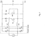
- the converter in fig. 1 is illustrated during a positive half cycle of the AC input voltage.
- the diodes in dashed lines are not conducting.
- several issues have occurred.
- the current is flowing into the converter in inductor Lb1 and the return current through Lb2 and D4.
- the current is distributed between the diode D4 and the inductor Lb2 so that the entire ripple current is flowing through the diode and the remaining DC-current without any ripple is flowing in the inductor Lb2.
- the present invention provides a device arranged for converting an AC input voltage to a DC output voltage comprising a bridgeless boost converter and protection and stabilisation system where the above disadvantages are avoided.
- the object of the invention is also to contribute to increased power efficiency for the power supply system.
- the present invention relates to a device arranged for converting an AC input voltage to a DC output voltage, comprising:
- the protection and stabilisation system comprises one capacitor in parallel with the second diode and one capacitor in parallel with the fourth diode.
- the capacitor in parallel with the second diode is referred to as the second capacitor and the capacitor in parallel with the fourth diode is referred to as the fourth capacitor.
- the protection and stabilisation system comprises one capacitor in parallel with the first diode and one capacitor in parallel with the third diode.
- the capacitor in parallel with first diode is referred to as the first capacitor and the capacitor in parallel with the third diode is referred to as the third capacitor.
- the bridgeless boost converter comprises:
- the boost inductor device comprises a first boost inductor having a first end connected to the first AC input terminal and a second end connected to a first node; and a second boost inductor having a first end connected to the second AC input terminal and a second end connected to a second node.
- the boost diode device comprises a first boost diode having an anode connected to the first node and a cathode connected to the positive boost output terminal and a second boost diode having an anode connected to the second node and cathode connected to the positive boost output terminal.
- the boost switch device comprises a first boost switch connected between the first node and the negative output boost terminal and a second boost switch connected between the second node and the negative output boost terminal.
- the boost capacitor device comprises a boost capacitor connected between the positive boost output terminal and the negative boost output terminal.
- Fig. 4 shows an embodiment of a device for converting an AC input voltage to a DC output voltage.
- the AC voltage is normally the AC mains.
- the DC output voltage can be supplied directly to a load or can be supplied to a DC-DC converter for further improving the quality of the DC voltage delivered to a load.
- the device arranged for converting an AC input voltage to a DC output voltage comprises a bridgeless boost converter and a protection and stabilisation system.
- the protection and stabilisation system comprises:
- the anode of the first diode D1 is connected to the first AC input terminal and the cathode of the first diode D1 is connected to the positive boost output terminal Obp.
- the bridgeless boost converter comprises:
- the boost diode device comprises a first boost diode Db1 having an anode connected to the first node 1 and a cathode connected to the positive boost output terminal Obp and a second boost diode Db2 having an anode connected to the second node 2 and a cathode connected to the positive boost output terminal Obp.
- the boost switch device comprising a first boost switch Sb1 connected between the first node 1 and the negative output boost terminal Obn and a second boost switch Sb2 connected between the second node 2 and the negative output boost terminal Obn.
- the boost capacitor device comprises a boost capacitor Cb1 connected between the positive boost output terminal Obp and the negative boost output terminal Obn.
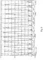
- fig. 5 showing a simulation of the voltage Vcm of the device described above with reference to fig. 4 . It can be seen that the voltage Vcm varies from approximately -1V to +2V, which is a considerably reduction. It has been found that the device described above solves the problem mentioned in the introduction satisfactorily.
- fig. 6 showing the bridgeless boost converter as a box with solid lines. Consequently, it should be noted that the present invention is not limited to the bridgeless boost converter topology shown in fig. 4 , but it can be used together with several other bridgeless boost converters for example as shown and described in Huber, L. et al mentioned in the introduction.
- the switches are of type MOSFET switches.
- the switches are switches with intrinsic diodes or switches connected in parallel with anti-parallel diodes.
- Examples of alternative switches are IGBTs connected in parallel with anti-parallel diodes.
- the switches are controlled by a control system based on parameters such as measured voltages and/or currents.
- the method used by the control system for controlling the switches would be known for a man skilled in the art.
- the control system can be implemented by means of one or several analogue control circuits or digital signal processors.
Landscapes
- Engineering & Computer Science (AREA)
- Power Engineering (AREA)
- Rectifiers (AREA)
- Dc-Dc Converters (AREA)
Claims (9)
- Vorrichtung, die zum Umwandeln einer AC-Eingangsspannung in eine DC-Ausgangsspannung eingerichtet ist, Folgendes umfassend:- einen brückenlosen Hochsetzwandler; und- ein Schutz- und Stabilisierungssystem, das Folgendes umfasst:- eine erste Diode (D2), wobei die Anode an einen negativen Hochsetzausgangsanschluss (Obn) angeschlossen ist, und die Kathode an den ersten AC-Eingangsanschluss angeschlossen ist;- eine zweite Diode (D4), wobei die Anode an den negativen Hochsetzausgangsanschluss (Obn) angeschlossen ist, und die Kathode an den zweiten AC-Eingangsanschluss angeschlossen ist;- eine dritte Diode (D1), wobei die Anode an einen ersten AC-Eingangsanschluss angeschlossen ist, und die Kathode an einen positiven Hochsetzausgangsanschluss (Obp) angeschlossen ist; und- eine vierte Diode (D3), wobei die Anode an einen zweiten AC-Eingangsanschluss angeschlossen ist, und die Kathode an den positiven Hochsetzausgangsanschluss (Opb) angeschlossen ist;dadurch gekennzeichnet, dass das Schutz- und Stabilisierungssystem darüber hinaus umfasst mindestens ein Kondensator mit mindestens einer der Schutz- und Stabilisierungsdioden (D1 - D4) parallelgeschaltet ist.
- Vorrichtung nach Anspruch 1, wobei der brückenlose Hochsetzwandler umfasst:- eine Hochsetzinduktorvorrichtung mit mindestens zwei Hochsetzinduktoren;- eine Hochsetzdiodenvorrichtung mit mindestens zwei Hochsetzdioden;- eine Hochsetzschaltvorrichtung mit mindestens zwei Hochsetzschaltern; und- eine Hochsetzkondensatorvorrichtung mit mindestens einem Hochsetzkondensator.
- Vorrichtung nach Anspruch 1, wobei das Schutz- und Stabilisierungssystem einen mit der ersten Diode (D2) parallelen Kondensator (C2) und einen mit der zweiten Diode (D4) parallelen Kondensator (C4) umfasst.
- Vorrichtung nach Anspruch 3, wobei das Schutz- und Stabilisierungssystem einen mit der dritten Diode (D1) parallelen Kondensator (C1) und einen mit der vierten Diode (D3) parallelen Kondensator (C3) umfasst.
- Vorrichtung nach einem der vorhergehenden Ansprüche, wobei:- die Hochsetzinduktorvorrichtung einen ersten Hochsetzinduktor (Lbl), von dem ein erstes Ende an den ersten AC-Eingangsanschluss und ein zweites Ende an einen ersten Knoten (1) angeschlossen ist, und einen zweiten Hochsetzinduktor (Lb2) umfasst, von dem ein erstes Ende an den zweiten AC-Eingangsanschluss und ein zweites Ende an einen zweiten Knoten (2) angeschlossen ist.
- Vorrichtung nach einem der vorhergehenden Ansprüche, wobei:- die Hochsetzdiodenvorrichtung eine erste Hochsetzdiode (Db1) mit einer an den ersten Knoten (1) angeschlossenen Anode und einer an den positiven Hochsetzausgangsanschluss (Obp) angeschlossenen Kathode und eine zweite Hochsetzdiode (Db2) mit einer an den zweiten Knoten (2) angeschlossenen Anode und einer an den positiven Hochsetzausgangsanschluss (Obp) angeschlossenen Kathode umfasst.
- Vorrichtung nach einem der vorhergehenden Ansprüche, wobei:- die Hochsetzschaltvorrichtung einen ersten Hochsetzschalter (Sb1), der zwischen dem ersten Knoten (1) und dem negativen Hochsetzausgangsanschluss (Obn) angeschlossen ist, und einen zweiten Hochsetzschalter (Sb2) umfasst, der zwischen dem zweiten Knoten (2) und dem negativen Hochsetzausgangsanschluss (Obn) angeschlossen ist.
- Vorrichtung nach einem der vorhergehenden Ansprüche, wobei:- die Hochsetzkondensatorvorrichtung einen Hochsetzkondensator (Cb1) umfasst, der zwischen dem positiven Hochsetzausgangsanschluss (Obp) und dem negativen Hochsetzausgangsanschluss (Obn) angeschlossen ist.
- Vorrichtung nach Anspruch 2, wobei:- die Hochsetzinduktorvorrichtung einen ersten Hochsetzinduktor (Lbl), von dem ein erstes Ende an den ersten AC-Eingangsanschluss und ein zweites Ende an einen ersten Knoten (1) angeschlossen ist, und einen zweiten Hochsetzinduktor (Lb2) umfasst, von dem ein erstes Ende an den zweiten AC-Eingangsanschluss und ein zweites Ende an einen zweiten Knoten (2) angeschlossen ist- die Hochsetzdiodenvorrichtung eine erste Hochsetzdiode (Db1), die zwischen dem ersten Knoten (1) und dem positiven Hochsetzausgangsanschluss (Obp) angeschlossen ist, und eine zweite Hochsetzdiode (Db2) umfasst, die zwischen dem zweiten Knoten (2) und dem positiven Hochsetzausgangsanschluss (Obp) angeschlossen ist;- die Hochsetzschaltvorrichtung einen ersten Hochsetzschalter (Sb1), der zwischen dem ersten Knoten (1) und dem negativen Hochsetzausgangsanschluss (Obn) angeschlossen ist, und einen zweiten Hochsetzschalter (Sb2) umfasst, der zwischen dem zweiten Knoten (2) und dem negativen Hochsetzausgangsanschluss (Obn) angeschlossen ist; und- die Hochsetzkondensatorvorrichtung einen ersten Hochsetzkondensator (Cb1) umfasst, der zwischen dem positiven Hochsetzausgangsanschluss (Obp) und dem negativen Hochsetzausgangsanschluss (Obn) angeschlossen ist.
Applications Claiming Priority (3)
| Application Number | Priority Date | Filing Date | Title |
|---|---|---|---|
| US98393907P | 2007-10-31 | 2007-10-31 | |
| GB0721420A GB2454217A (en) | 2007-10-31 | 2007-10-31 | AC to DC bridgeless boost converter with protection and stabilisation |
| PCT/NO2008/000384 WO2009058025A1 (en) | 2007-10-31 | 2008-10-30 | Device arranged for converting an ac input voltage to a dc output voltage |
Publications (3)
| Publication Number | Publication Date |
|---|---|
| EP2218169A1 EP2218169A1 (de) | 2010-08-18 |
| EP2218169B1 EP2218169B1 (de) | 2012-04-25 |
| EP2218169B2 true EP2218169B2 (de) | 2020-01-08 |
Family
ID=38834637
Family Applications (1)
| Application Number | Title | Priority Date | Filing Date |
|---|---|---|---|
| EP08844429.4A Not-in-force EP2218169B2 (de) | 2007-10-31 | 2008-10-30 | Wechselstrom-gleichstrom-aufwärtswandler ohne brücke |
Country Status (4)
| Country | Link |
|---|---|
| EP (1) | EP2218169B2 (de) |
| AT (1) | ATE555538T1 (de) |
| GB (1) | GB2454217A (de) |
| WO (1) | WO2009058025A1 (de) |
Families Citing this family (7)
| Publication number | Priority date | Publication date | Assignee | Title |
|---|---|---|---|---|
| CN102714460B (zh) * | 2010-10-07 | 2016-06-22 | 富士电机株式会社 | 功率转换设备 |
| JP5772367B2 (ja) * | 2011-08-08 | 2015-09-02 | 富士電機株式会社 | 直流電源装置用力率改善回路 |
| EP2654374A1 (de) * | 2012-04-20 | 2013-10-23 | Koninklijke Philips N.V. | Gleichrichterschaltung mit Kondensatoren zur Versorgung von LEDs |
| PL2859778T3 (pl) | 2013-04-26 | 2016-02-29 | Philips Lighting Holding Bv | Urządzenie oświetlające odpowiednie do kilku źródeł napięcia |
| CN104467390A (zh) * | 2014-11-26 | 2015-03-25 | 无锡上能新能源有限公司 | 一种换流器保护电路及包括该电路的换流器 |
| KR101818952B1 (ko) | 2017-06-01 | 2018-02-28 | 주식회사 아이투알테크 | 정전원 공급장치 |
| CN109039074A (zh) * | 2018-09-13 | 2018-12-18 | 上海推拓科技有限公司 | 一种无桥三整流Boost电源电路 |
Family Cites Families (3)
| Publication number | Priority date | Publication date | Assignee | Title |
|---|---|---|---|---|
| US4626981A (en) * | 1985-08-02 | 1986-12-02 | Rca Corporation | Dual voltage converter circuit |
| FI81701C (fi) * | 1988-05-17 | 1990-11-12 | Kone Oy | Oeverspaenningsskydd foer riktarbryggor. |
| DE9216662U1 (de) * | 1992-12-07 | 1993-01-28 | Siemens AG, 80333 München | Vorladeschaltung mit kombiniertem Überspannungsschutz für einen netzgeführten Stromrichter mit ausgangsseitigem Kondensator |
-
2007
- 2007-10-31 GB GB0721420A patent/GB2454217A/en not_active Withdrawn
-
2008
- 2008-10-30 WO PCT/NO2008/000384 patent/WO2009058025A1/en not_active Ceased
- 2008-10-30 AT AT08844429T patent/ATE555538T1/de active
- 2008-10-30 EP EP08844429.4A patent/EP2218169B2/de not_active Not-in-force
Also Published As
| Publication number | Publication date |
|---|---|
| EP2218169A1 (de) | 2010-08-18 |
| ATE555538T1 (de) | 2012-05-15 |
| WO2009058025A1 (en) | 2009-05-07 |
| EP2218169B1 (de) | 2012-04-25 |
| GB2454217A (en) | 2009-05-06 |
| GB0721420D0 (en) | 2007-12-12 |
Similar Documents
| Publication | Publication Date | Title |
|---|---|---|
| EP2215709B2 (de) | Einrichtung zum umsetzen einer eingangswechselspannung in eine ausgangsgleichspannung | |
| US6950319B2 (en) | AC/DC flyback converter | |
| Tofoli et al. | Novel nonisolated high-voltage gain dc–dc converters based on 3SSC and VMC | |
| EP2218169B1 (de) | Wechselstrom-gleichstrom-aufwärtswandler ohne brücke | |
| US9899910B2 (en) | Bridgeless PFC power converter with reduced EMI noise | |
| JP6180126B2 (ja) | 力率改善回路及び力率改善制御方法 | |
| WO2016101058A1 (en) | Flyback converter | |
| Franco de Souza et al. | Experimental evaluation of active power factor correction techniques in a single‐phase AC‐DC boost converter | |
| US6519164B1 (en) | Single power stage AC/DC forward converter with power switch voltage clamping function | |
| Castro et al. | An AC–DC PFC single-stage dual inductor current-fed push–pull for HB-LED lighting applications | |
| Ekemezie | Design of a power factor correction ac-dc converter | |
| Zhang et al. | An improved CCM single-stage PFC converter with a low frequency auxiliary switch | |
| XueChao et al. | UCC28070 implement bridgeless power factor correction (PFC) pre-regulator design | |
| EP4123893A1 (de) | Aktiver gleichrichter in einem schaltnetzteil | |
| CN116800081A (zh) | 服务器电源电路、服务器电源的过压保护方法及装置 | |
| Abdel-Rahman et al. | CoolGaN™ totem-pole PFC design guide and power loss modeling | |
| Li et al. | A high efficiency and high power density asymmetrical half-bridge flyback converter for data centers | |
| WO2006137744A1 (en) | Control method and device for a converter using a three-state switching cell | |
| Maniak | Effect of clamp-type surge protection circuit configurations on EMC emissions from a flyback converter | |
| Rashmi et al. | Design of symmetrical half-bridge converter with a series coupling capacitor | |
| Thandapani et al. | Modular power supply for telecom application (54v/100a) | |
| Tamyürek | Design of a three-phase unity power factor single-stage telecom rectifier | |
| MANIAK | University of Science and Technology of Oran," USTO-MB", Oran, Algeria. | |
| Tonolo et al. | An Interleaved Current-Fed PFC Flyback Converter With Voltage Follower Characteristic | |
| Siddique | Totem-pole power factor correction rectifier with Gallium-Nitride devices for telecom power supply |
Legal Events
| Date | Code | Title | Description |
|---|---|---|---|
| PUAI | Public reference made under article 153(3) epc to a published international application that has entered the european phase |
Free format text: ORIGINAL CODE: 0009012 |
|
| 17P | Request for examination filed |
Effective date: 20100531 |
|
| AK | Designated contracting states |
Kind code of ref document: A1 Designated state(s): AT BE BG CH CY CZ DE DK EE ES FI FR GB GR HR HU IE IS IT LI LT LU LV MC MT NL NO PL PT RO SE SI SK TR |
|
| AX | Request for extension of the european patent |
Extension state: AL BA MK RS |
|
| DAX | Request for extension of the european patent (deleted) | ||
| GRAP | Despatch of communication of intention to grant a patent |
Free format text: ORIGINAL CODE: EPIDOSNIGR1 |
|
| RTI1 | Title (correction) |
Free format text: BRIDGELESS BOOST AC-DC CONVERTER |
|
| GRAS | Grant fee paid |
Free format text: ORIGINAL CODE: EPIDOSNIGR3 |
|
| GRAA | (expected) grant |
Free format text: ORIGINAL CODE: 0009210 |
|
| AK | Designated contracting states |
Kind code of ref document: B1 Designated state(s): AT BE BG CH CY CZ DE DK EE ES FI FR GB GR HR HU IE IS IT LI LT LU LV MC MT NL NO PL PT RO SE SI SK TR |
|
| REG | Reference to a national code |
Ref country code: GB Ref legal event code: FG4D |
|
| REG | Reference to a national code |
Ref country code: CH Ref legal event code: EP |
|
| REG | Reference to a national code |
Ref country code: AT Ref legal event code: REF Ref document number: 555538 Country of ref document: AT Kind code of ref document: T Effective date: 20120515 |
|
| REG | Reference to a national code |
Ref country code: IE Ref legal event code: FG4D |
|
| REG | Reference to a national code |
Ref country code: DE Ref legal event code: R096 Ref document number: 602008015259 Country of ref document: DE Effective date: 20120621 |
|
| REG | Reference to a national code |
Ref country code: NL Ref legal event code: VDEP Effective date: 20120425 |
|
| REG | Reference to a national code |
Ref country code: AT Ref legal event code: MK05 Ref document number: 555538 Country of ref document: AT Kind code of ref document: T Effective date: 20120425 |
|
| LTIE | Lt: invalidation of european patent or patent extension |
Effective date: 20120425 |
|
| PG25 | Lapsed in a contracting state [announced via postgrant information from national office to epo] |
Ref country code: PL Free format text: LAPSE BECAUSE OF FAILURE TO SUBMIT A TRANSLATION OF THE DESCRIPTION OR TO PAY THE FEE WITHIN THE PRESCRIBED TIME-LIMIT Effective date: 20120425 Ref country code: SE Free format text: LAPSE BECAUSE OF FAILURE TO SUBMIT A TRANSLATION OF THE DESCRIPTION OR TO PAY THE FEE WITHIN THE PRESCRIBED TIME-LIMIT Effective date: 20120425 Ref country code: FI Free format text: LAPSE BECAUSE OF FAILURE TO SUBMIT A TRANSLATION OF THE DESCRIPTION OR TO PAY THE FEE WITHIN THE PRESCRIBED TIME-LIMIT Effective date: 20120425 Ref country code: IS Free format text: LAPSE BECAUSE OF FAILURE TO SUBMIT A TRANSLATION OF THE DESCRIPTION OR TO PAY THE FEE WITHIN THE PRESCRIBED TIME-LIMIT Effective date: 20120825 Ref country code: CY Free format text: LAPSE BECAUSE OF FAILURE TO SUBMIT A TRANSLATION OF THE DESCRIPTION OR TO PAY THE FEE WITHIN THE PRESCRIBED TIME-LIMIT Effective date: 20120425 Ref country code: NO Free format text: LAPSE BECAUSE OF FAILURE TO SUBMIT A TRANSLATION OF THE DESCRIPTION OR TO PAY THE FEE WITHIN THE PRESCRIBED TIME-LIMIT Effective date: 20120725 Ref country code: LT Free format text: LAPSE BECAUSE OF FAILURE TO SUBMIT A TRANSLATION OF THE DESCRIPTION OR TO PAY THE FEE WITHIN THE PRESCRIBED TIME-LIMIT Effective date: 20120425 |
|
| PG25 | Lapsed in a contracting state [announced via postgrant information from national office to epo] |
Ref country code: HR Free format text: LAPSE BECAUSE OF FAILURE TO SUBMIT A TRANSLATION OF THE DESCRIPTION OR TO PAY THE FEE WITHIN THE PRESCRIBED TIME-LIMIT Effective date: 20120425 Ref country code: LV Free format text: LAPSE BECAUSE OF FAILURE TO SUBMIT A TRANSLATION OF THE DESCRIPTION OR TO PAY THE FEE WITHIN THE PRESCRIBED TIME-LIMIT Effective date: 20120425 Ref country code: GR Free format text: LAPSE BECAUSE OF FAILURE TO SUBMIT A TRANSLATION OF THE DESCRIPTION OR TO PAY THE FEE WITHIN THE PRESCRIBED TIME-LIMIT Effective date: 20120726 Ref country code: SI Free format text: LAPSE BECAUSE OF FAILURE TO SUBMIT A TRANSLATION OF THE DESCRIPTION OR TO PAY THE FEE WITHIN THE PRESCRIBED TIME-LIMIT Effective date: 20120425 Ref country code: PT Free format text: LAPSE BECAUSE OF FAILURE TO SUBMIT A TRANSLATION OF THE DESCRIPTION OR TO PAY THE FEE WITHIN THE PRESCRIBED TIME-LIMIT Effective date: 20120827 |
|
| PG25 | Lapsed in a contracting state [announced via postgrant information from national office to epo] |
Ref country code: BE Free format text: LAPSE BECAUSE OF FAILURE TO SUBMIT A TRANSLATION OF THE DESCRIPTION OR TO PAY THE FEE WITHIN THE PRESCRIBED TIME-LIMIT Effective date: 20120425 |
|
| PLBI | Opposition filed |
Free format text: ORIGINAL CODE: 0009260 |
|
| PG25 | Lapsed in a contracting state [announced via postgrant information from national office to epo] |
Ref country code: AT Free format text: LAPSE BECAUSE OF FAILURE TO SUBMIT A TRANSLATION OF THE DESCRIPTION OR TO PAY THE FEE WITHIN THE PRESCRIBED TIME-LIMIT Effective date: 20120425 Ref country code: EE Free format text: LAPSE BECAUSE OF FAILURE TO SUBMIT A TRANSLATION OF THE DESCRIPTION OR TO PAY THE FEE WITHIN THE PRESCRIBED TIME-LIMIT Effective date: 20120425 Ref country code: RO Free format text: LAPSE BECAUSE OF FAILURE TO SUBMIT A TRANSLATION OF THE DESCRIPTION OR TO PAY THE FEE WITHIN THE PRESCRIBED TIME-LIMIT Effective date: 20120425 Ref country code: SK Free format text: LAPSE BECAUSE OF FAILURE TO SUBMIT A TRANSLATION OF THE DESCRIPTION OR TO PAY THE FEE WITHIN THE PRESCRIBED TIME-LIMIT Effective date: 20120425 Ref country code: CZ Free format text: LAPSE BECAUSE OF FAILURE TO SUBMIT A TRANSLATION OF THE DESCRIPTION OR TO PAY THE FEE WITHIN THE PRESCRIBED TIME-LIMIT Effective date: 20120425 Ref country code: DK Free format text: LAPSE BECAUSE OF FAILURE TO SUBMIT A TRANSLATION OF THE DESCRIPTION OR TO PAY THE FEE WITHIN THE PRESCRIBED TIME-LIMIT Effective date: 20120425 Ref country code: NL Free format text: LAPSE BECAUSE OF FAILURE TO SUBMIT A TRANSLATION OF THE DESCRIPTION OR TO PAY THE FEE WITHIN THE PRESCRIBED TIME-LIMIT Effective date: 20120425 |
|
| 26 | Opposition filed |
Opponent name: AEG POWER SOLUTIONS B.V. Effective date: 20130121 |
|
| PG25 | Lapsed in a contracting state [announced via postgrant information from national office to epo] |
Ref country code: IT Free format text: LAPSE BECAUSE OF FAILURE TO SUBMIT A TRANSLATION OF THE DESCRIPTION OR TO PAY THE FEE WITHIN THE PRESCRIBED TIME-LIMIT Effective date: 20120425 |
|
| PLAX | Notice of opposition and request to file observation + time limit sent |
Free format text: ORIGINAL CODE: EPIDOSNOBS2 |
|
| REG | Reference to a national code |
Ref country code: DE Ref legal event code: R026 Ref document number: 602008015259 Country of ref document: DE Effective date: 20130121 |
|
| PG25 | Lapsed in a contracting state [announced via postgrant information from national office to epo] |
Ref country code: ES Free format text: LAPSE BECAUSE OF FAILURE TO SUBMIT A TRANSLATION OF THE DESCRIPTION OR TO PAY THE FEE WITHIN THE PRESCRIBED TIME-LIMIT Effective date: 20120805 |
|
| PG25 | Lapsed in a contracting state [announced via postgrant information from national office to epo] |
Ref country code: MC Free format text: LAPSE BECAUSE OF NON-PAYMENT OF DUE FEES Effective date: 20121031 |
|
| REG | Reference to a national code |
Ref country code: CH Ref legal event code: PL |
|
| PLBB | Reply of patent proprietor to notice(s) of opposition received |
Free format text: ORIGINAL CODE: EPIDOSNOBS3 |
|
| PG25 | Lapsed in a contracting state [announced via postgrant information from national office to epo] |
Ref country code: CH Free format text: LAPSE BECAUSE OF NON-PAYMENT OF DUE FEES Effective date: 20121031 Ref country code: LI Free format text: LAPSE BECAUSE OF NON-PAYMENT OF DUE FEES Effective date: 20121031 Ref country code: BG Free format text: LAPSE BECAUSE OF FAILURE TO SUBMIT A TRANSLATION OF THE DESCRIPTION OR TO PAY THE FEE WITHIN THE PRESCRIBED TIME-LIMIT Effective date: 20120725 |
|
| REG | Reference to a national code |
Ref country code: IE Ref legal event code: MM4A |
|
| PG25 | Lapsed in a contracting state [announced via postgrant information from national office to epo] |
Ref country code: IE Free format text: LAPSE BECAUSE OF NON-PAYMENT OF DUE FEES Effective date: 20121030 |
|
| PG25 | Lapsed in a contracting state [announced via postgrant information from national office to epo] |
Ref country code: MT Free format text: LAPSE BECAUSE OF FAILURE TO SUBMIT A TRANSLATION OF THE DESCRIPTION OR TO PAY THE FEE WITHIN THE PRESCRIBED TIME-LIMIT Effective date: 20120425 |
|
| PG25 | Lapsed in a contracting state [announced via postgrant information from national office to epo] |
Ref country code: TR Free format text: LAPSE BECAUSE OF FAILURE TO SUBMIT A TRANSLATION OF THE DESCRIPTION OR TO PAY THE FEE WITHIN THE PRESCRIBED TIME-LIMIT Effective date: 20120425 |
|
| PG25 | Lapsed in a contracting state [announced via postgrant information from national office to epo] |
Ref country code: LU Free format text: LAPSE BECAUSE OF NON-PAYMENT OF DUE FEES Effective date: 20121030 |
|
| PG25 | Lapsed in a contracting state [announced via postgrant information from national office to epo] |
Ref country code: HU Free format text: LAPSE BECAUSE OF FAILURE TO SUBMIT A TRANSLATION OF THE DESCRIPTION OR TO PAY THE FEE WITHIN THE PRESCRIBED TIME-LIMIT Effective date: 20081030 |
|
| APBM | Appeal reference recorded |
Free format text: ORIGINAL CODE: EPIDOSNREFNO |
|
| APBP | Date of receipt of notice of appeal recorded |
Free format text: ORIGINAL CODE: EPIDOSNNOA2O |
|
| APAH | Appeal reference modified |
Free format text: ORIGINAL CODE: EPIDOSCREFNO |
|
| APBQ | Date of receipt of statement of grounds of appeal recorded |
Free format text: ORIGINAL CODE: EPIDOSNNOA3O |
|
| REG | Reference to a national code |
Ref country code: FR Ref legal event code: PLFP Year of fee payment: 8 |
|
| REG | Reference to a national code |
Ref country code: FR Ref legal event code: PLFP Year of fee payment: 9 |
|
| REG | Reference to a national code |
Ref country code: FR Ref legal event code: PLFP Year of fee payment: 10 |
|
| REG | Reference to a national code |
Ref country code: FR Ref legal event code: PLFP Year of fee payment: 11 |
|
| APBU | Appeal procedure closed |
Free format text: ORIGINAL CODE: EPIDOSNNOA9O |
|
| PLAB | Opposition data, opponent's data or that of the opponent's representative modified |
Free format text: ORIGINAL CODE: 0009299OPPO |
|
| PUAH | Patent maintained in amended form |
Free format text: ORIGINAL CODE: 0009272 |
|
| STAA | Information on the status of an ep patent application or granted ep patent |
Free format text: STATUS: PATENT MAINTAINED AS AMENDED |
|
| R26 | Opposition filed (corrected) |
Opponent name: AEG POWER SOLUTIONS B.V. Effective date: 20130121 |
|
| 27A | Patent maintained in amended form |
Effective date: 20200108 |
|
| AK | Designated contracting states |
Kind code of ref document: B2 Designated state(s): AT BE BG CH CY CZ DE DK EE ES FI FR GB GR HR HU IE IS IT LI LT LU LV MC MT NL NO PL PT RO SE SI SK TR |
|
| REG | Reference to a national code |
Ref country code: DE Ref legal event code: R102 Ref document number: 602008015259 Country of ref document: DE |
|
| PGFP | Annual fee paid to national office [announced via postgrant information from national office to epo] |
Ref country code: FR Payment date: 20191219 Year of fee payment: 13 |
|
| PGFP | Annual fee paid to national office [announced via postgrant information from national office to epo] |
Ref country code: GB Payment date: 20201022 Year of fee payment: 13 Ref country code: DE Payment date: 20201022 Year of fee payment: 13 |
|
| REG | Reference to a national code |
Ref country code: DE Ref legal event code: R119 Ref document number: 602008015259 Country of ref document: DE |
|
| GBPC | Gb: european patent ceased through non-payment of renewal fee |
Effective date: 20211030 |
|
| PG25 | Lapsed in a contracting state [announced via postgrant information from national office to epo] |
Ref country code: GB Free format text: LAPSE BECAUSE OF NON-PAYMENT OF DUE FEES Effective date: 20211030 Ref country code: DE Free format text: LAPSE BECAUSE OF NON-PAYMENT OF DUE FEES Effective date: 20220503 |
|
| PG25 | Lapsed in a contracting state [announced via postgrant information from national office to epo] |
Ref country code: FR Free format text: LAPSE BECAUSE OF NON-PAYMENT OF DUE FEES Effective date: 20211031 |