EP2218109B1 - Methods for manufacturing solar cell module and apparatus for manufacturing the same - Google Patents
Methods for manufacturing solar cell module and apparatus for manufacturing the same Download PDFInfo
- Publication number
- EP2218109B1 EP2218109B1 EP08856189.9A EP08856189A EP2218109B1 EP 2218109 B1 EP2218109 B1 EP 2218109B1 EP 08856189 A EP08856189 A EP 08856189A EP 2218109 B1 EP2218109 B1 EP 2218109B1
- Authority
- EP
- European Patent Office
- Prior art keywords
- solar cell
- laser
- compressing
- contact portion
- metal ribbon
- Prior art date
- Legal status (The legal status is an assumption and is not a legal conclusion. Google has not performed a legal analysis and makes no representation as to the accuracy of the status listed.)
- Not-in-force
Links
- 238000000034 method Methods 0.000 title claims description 83
- 238000004519 manufacturing process Methods 0.000 title claims description 15
- 239000002184 metal Substances 0.000 claims description 72
- 229910052751 metal Inorganic materials 0.000 claims description 72
- 238000010438 heat treatment Methods 0.000 claims description 22
- 239000000523 sample Substances 0.000 claims description 15
- MCMNRKCIXSYSNV-UHFFFAOYSA-N Zirconium dioxide Chemical compound O=[Zr]=O MCMNRKCIXSYSNV-UHFFFAOYSA-N 0.000 claims description 14
- 239000000919 ceramic Substances 0.000 claims description 10
- 230000001678 irradiating effect Effects 0.000 claims description 8
- 239000011521 glass Substances 0.000 claims description 3
- 239000010453 quartz Substances 0.000 claims description 3
- VYPSYNLAJGMNEJ-UHFFFAOYSA-N silicon dioxide Inorganic materials O=[Si]=O VYPSYNLAJGMNEJ-UHFFFAOYSA-N 0.000 claims description 3
- 238000005507 spraying Methods 0.000 claims description 2
- 238000007906 compression Methods 0.000 description 9
- 239000013078 crystal Substances 0.000 description 9
- 230000006835 compression Effects 0.000 description 7
- 230000005855 radiation Effects 0.000 description 7
- XUIMIQQOPSSXEZ-UHFFFAOYSA-N Silicon Chemical compound [Si] XUIMIQQOPSSXEZ-UHFFFAOYSA-N 0.000 description 5
- 239000011247 coating layer Substances 0.000 description 5
- 230000008602 contraction Effects 0.000 description 5
- 230000006378 damage Effects 0.000 description 5
- 239000010410 layer Substances 0.000 description 5
- 239000007769 metal material Substances 0.000 description 5
- 229910052710 silicon Inorganic materials 0.000 description 5
- 239000010703 silicon Substances 0.000 description 5
- 230000007547 defect Effects 0.000 description 4
- 239000000463 material Substances 0.000 description 4
- 238000011109 contamination Methods 0.000 description 3
- 230000002950 deficient Effects 0.000 description 3
- 150000002222 fluorine compounds Chemical class 0.000 description 3
- 238000002844 melting Methods 0.000 description 3
- 230000008018 melting Effects 0.000 description 3
- 229920001296 polysiloxane Polymers 0.000 description 3
- 229910045601 alloy Inorganic materials 0.000 description 2
- 239000000956 alloy Substances 0.000 description 2
- 230000003247 decreasing effect Effects 0.000 description 2
- 239000000835 fiber Substances 0.000 description 2
- 230000000704 physical effect Effects 0.000 description 2
- 241000123069 Ocyurus chrysurus Species 0.000 description 1
- 229910052782 aluminium Inorganic materials 0.000 description 1
- PNEYBMLMFCGWSK-UHFFFAOYSA-N aluminium oxide Inorganic materials [O-2].[O-2].[O-2].[Al+3].[Al+3] PNEYBMLMFCGWSK-UHFFFAOYSA-N 0.000 description 1
- 230000006399 behavior Effects 0.000 description 1
- 230000015556 catabolic process Effects 0.000 description 1
- 238000007796 conventional method Methods 0.000 description 1
- 238000001816 cooling Methods 0.000 description 1
- 229910052802 copper Inorganic materials 0.000 description 1
- RKTYLMNFRDHKIL-UHFFFAOYSA-N copper;5,10,15,20-tetraphenylporphyrin-22,24-diide Chemical compound [Cu+2].C1=CC(C(=C2C=CC([N-]2)=C(C=2C=CC=CC=2)C=2C=CC(N=2)=C(C=2C=CC=CC=2)C2=CC=C3[N-]2)C=2C=CC=CC=2)=NC1=C3C1=CC=CC=C1 RKTYLMNFRDHKIL-UHFFFAOYSA-N 0.000 description 1
- 229910052593 corundum Inorganic materials 0.000 description 1
- 229910021419 crystalline silicon Inorganic materials 0.000 description 1
- 238000006731 degradation reaction Methods 0.000 description 1
- 230000000694 effects Effects 0.000 description 1
- 238000003912 environmental pollution Methods 0.000 description 1
- 229910052736 halogen Inorganic materials 0.000 description 1
- 150000002367 halogens Chemical class 0.000 description 1
- 238000009434 installation Methods 0.000 description 1
- 229910021421 monocrystalline silicon Inorganic materials 0.000 description 1
- 239000013307 optical fiber Substances 0.000 description 1
- 239000012466 permeate Substances 0.000 description 1
- 239000005365 phosphate glass Substances 0.000 description 1
- 238000010248 power generation Methods 0.000 description 1
- 239000010979 ruby Substances 0.000 description 1
- 229910001750 ruby Inorganic materials 0.000 description 1
- 239000005368 silicate glass Substances 0.000 description 1
- 238000005476 soldering Methods 0.000 description 1
- 239000007921 spray Substances 0.000 description 1
- 230000035882 stress Effects 0.000 description 1
- 238000004381 surface treatment Methods 0.000 description 1
- 229910019655 synthetic inorganic crystalline material Inorganic materials 0.000 description 1
- 230000003685 thermal hair damage Effects 0.000 description 1
- 230000008646 thermal stress Effects 0.000 description 1
- 229910052718 tin Inorganic materials 0.000 description 1
- 239000012780 transparent material Substances 0.000 description 1
- 229910001845 yogo sapphire Inorganic materials 0.000 description 1
- 229910019901 yttrium aluminum garnet Inorganic materials 0.000 description 1
Images





Classifications
-
- H—ELECTRICITY
- H10—SEMICONDUCTOR DEVICES; ELECTRIC SOLID-STATE DEVICES NOT OTHERWISE PROVIDED FOR
- H10F—INORGANIC SEMICONDUCTOR DEVICES SENSITIVE TO INFRARED RADIATION, LIGHT, ELECTROMAGNETIC RADIATION OF SHORTER WAVELENGTH OR CORPUSCULAR RADIATION
- H10F71/00—Manufacture or treatment of devices covered by this subclass
-
- H—ELECTRICITY
- H10—SEMICONDUCTOR DEVICES; ELECTRIC SOLID-STATE DEVICES NOT OTHERWISE PROVIDED FOR
- H10F—INORGANIC SEMICONDUCTOR DEVICES SENSITIVE TO INFRARED RADIATION, LIGHT, ELECTROMAGNETIC RADIATION OF SHORTER WAVELENGTH OR CORPUSCULAR RADIATION
- H10F77/00—Constructional details of devices covered by this subclass
- H10F77/20—Electrodes
- H10F77/206—Electrodes for devices having potential barriers
- H10F77/211—Electrodes for devices having potential barriers for photovoltaic cells
-
- H—ELECTRICITY
- H10—SEMICONDUCTOR DEVICES; ELECTRIC SOLID-STATE DEVICES NOT OTHERWISE PROVIDED FOR
- H10F—INORGANIC SEMICONDUCTOR DEVICES SENSITIVE TO INFRARED RADIATION, LIGHT, ELECTROMAGNETIC RADIATION OF SHORTER WAVELENGTH OR CORPUSCULAR RADIATION
- H10F19/00—Integrated devices, or assemblies of multiple devices, comprising at least one photovoltaic cell covered by group H10F10/00, e.g. photovoltaic modules
-
- H—ELECTRICITY
- H10—SEMICONDUCTOR DEVICES; ELECTRIC SOLID-STATE DEVICES NOT OTHERWISE PROVIDED FOR
- H10F—INORGANIC SEMICONDUCTOR DEVICES SENSITIVE TO INFRARED RADIATION, LIGHT, ELECTROMAGNETIC RADIATION OF SHORTER WAVELENGTH OR CORPUSCULAR RADIATION
- H10F71/00—Manufacture or treatment of devices covered by this subclass
- H10F71/137—Batch treatment of the devices
- H10F71/1375—Apparatus for automatic interconnection of photovoltaic cells in a module
-
- Y—GENERAL TAGGING OF NEW TECHNOLOGICAL DEVELOPMENTS; GENERAL TAGGING OF CROSS-SECTIONAL TECHNOLOGIES SPANNING OVER SEVERAL SECTIONS OF THE IPC; TECHNICAL SUBJECTS COVERED BY FORMER USPC CROSS-REFERENCE ART COLLECTIONS [XRACs] AND DIGESTS
- Y02—TECHNOLOGIES OR APPLICATIONS FOR MITIGATION OR ADAPTATION AGAINST CLIMATE CHANGE
- Y02E—REDUCTION OF GREENHOUSE GAS [GHG] EMISSIONS, RELATED TO ENERGY GENERATION, TRANSMISSION OR DISTRIBUTION
- Y02E10/00—Energy generation through renewable energy sources
- Y02E10/50—Photovoltaic [PV] energy
Definitions
- the present invention relates to a method for manufacturing a solar cell module and an apparatus therefor.
- a solar cell module which is an essential element in a solar photovoltaic power generation system, has advantages in that a lifetime of about 20 years or more so that it may be semi-permanently used, and a large-sized solar cell module as well as a small-sized solar cell module can be freely manufactured depending on installation locations and scales.
- a thermal bonding process by which solar cells are modularized by being connected to one another in series via power lines, i.e., metal electrodes(ribbons), is referred to as a tabbing or soldering process.
- a conventional tabbing process is performed in such a manner that a bonding portion between a metal electrode (or ribbon) and a solar cell is heated using a halogen infrared lamp (IR tabbing process) or manually welded by a worker.
- IR tabbing process halogen infrared lamp
- the IR tabbing process has a problem in that a zone directly irradiated by the infrared lamp is excessively larger than a bonding area required for the tabbing process so that a solar cell module may be more likely to be damaged during the tabbing process.
- a solar cell such as a crystal silicon solar cell has a multi-layered structure (e.g., including A1 coating layer, Si wafer layer and SiN 3 Ar coating layer) of which the layers are made of different materials. Accordingly, if a directly-irradiated zone is excessively large as described above in the same manner as the conventional IR tabbing process, differences in thermal expansion/contraction behaviors of the materials for the respective layers of the solar cell upon application of thermal energy thereto cause the solar cell module to be bent up to 3 mm, resulting in defects in the solar cell module, such as a crack, breakage, damage or warping.
- a directly-irradiated zone is excessively large as described above in the same manner as the conventional IR tabbing process, differences in thermal expansion/contraction behaviors of the materials for the respective layers of the solar cell upon application of thermal energy thereto cause the solar cell module to be bent up to 3 mm, resulting in defects in the solar cell module, such as a crack, breakage, damage or warping.
- Document JP 60 202968 A describes an apparatus and a method for bonding leads to solar cells, wherein the leads are compressed from the outside to the inside and a laser light is projected from projecting systems.
- An object of the present invention is to provide a method and apparatus for manufacturing a solar cell module, in which a bonding process between a metal electrode and the solar cell is performed by local heating with a laser, so that a fraction defective in the tabbing process can be reduced, the bonding strength and bonding uniformity can be improved, and the processing time can be reduced, thereby improving the productivity.
- an apparatus for manufacturing a solar cell module accodring to claim 7.
- a tabbing process of a solar cell and a metal electrode is performed by local heating with a laser, which can localize a heating zone to a minimally required area, so that a direct radiation zone to which thermal energy is directly radiated can be minimized during the process. Therefore, according to the present invention, there are advantages in that it is possible to reduce a fraction defective (generation of crack, breakage and damage) caused by different physical properties (thermal expansion/contraction coefficient) between materials of the solar cell configured to have a multi-layered structure, to provide the high and uniform bonding strength to the contact portion, and to reduce the processing time, thereby improving the production efficiency.
- the present invention is related to a method for manufacturing a solar cell module, which comprises: a first step of compressing a metal electrode onto a solar cell; and a second step of performing a tabbing process by irradiating a contact portion of the metal electrode and the solar cell with a laser.
- the first step of the present invention is a step of preparing a tabbing process by compressing a metal electrode onto a solar cell.
- the kind of solar cell onto which the metal electrode is compressed is not specifically limited, but a crystal silicon solar cell, such as a single crystal silicon solar cell and a polycrystalline silicone solar cell, may be included in an example of the solar cell.
- the method of the present invention may be effectively applied to a thinned solar cell, since a direct radiation zone and a mechanical stress (or thermal stress) applied to the thin solar cell can be minimized. Therefore, the solar cell applied to the present method may have a thickness ranging from 80 ⁇ m to 200 ⁇ m. If the thickness is less than 80 ⁇ m, it is apprehended that the efficiency of the solar cell is decreased. If the thickness is more than 200 ⁇ m, it is apprehended that economical efficiency is lowered.
- the kind of the metal electrode (ribbon) to be compressed in the first step of the present invention is not specifically limited, but all metal electrodes which have been conventionally used in a solar cell field may be included in an example of the metal electrode.
- a Cu electrode may be a representative example of the metal electrode as described above.
- a low melting point alloy layer e.g., an alloy layer of Cu, Sn and Al
- the metal electrode as described above has a width ranging from 1.5 mm to 2.5 mm and a thickness ranging from 80 ⁇ m to 300 ⁇ m.
- the present invention is not limited thereto, but various metal electrodes may be used.
- the metal electrodes are excessively thin, there is an advantage in that the power or scanning speed of a laser used in tabbing can be reduced, but the efficiency of a solar cell module may be decreased due to the increase of the electrode resistance. Therefore, it is preferable to select the electrode having an appropriate thickness according to applications.
- the metal electrode is compressed onto the solar cell in the first step of the present invention, at this time it is preferable that uniform pressure is applied with respect to the whole contact portions of the metal electrode and the solar cells. If uniform compression is not carried out, it is apprehended that the the metal electrode is not uniformly bonded to the solar cell, and thereby efficiency of the solar cell module is lowered due to electrical loss.
- the compression process may be carried out by using a compression device comprising probe pin, pressurizing plate, compressing roll or air-nozzle.
- the means for compression is not specifically limited only if the metal electrodes can be uniformly and closely compressed onto the solar cell.
- the metal electrodes be simultaneously compressed on front and rear surfaces of the solar cell in the first step of the present invention. That is, as shown in Fig. 1 , the metal electrodes 2 are tabbed on the left and right sides of the front surface of the solar cell 1, respectively. At this time, the metal electrodes are bonded onto the left and right sides of the rear surface of the solar cell as well as the left and right sides of the front surface of the solar cell. Accordingly, all the four metal electrodes are simultaneously compressed onto the left and right sides of the front and rear surfaces of the single solar cell in accordance with the present invention, respectively, and then, left and right sides thereof are irradiated with a laser, thereby performing the tabbing process.
- the heat to be generated by the laser applied to the upper portion is conducted to the lower portion, so that the tabbing process can be performed in the upper and lower portions simultaneously.
- the compression of the metal electrodes is performed at a pressure of 0.3 N/m to 0.6 N/m.
- the contact of the metal electrodes may be deteriorated if the pressure is smaller than 0.3 N/m, whereas the excessive pressure may damage the solar cell if the pressure is larger than 0.6 N/m.
- the tabbing process is performed by irradiating the contact portions of the solar cell and the metal electrode with a laser.
- Fig. 2 of the accompanying drawings is a schematic view showing a state where the tabbing process is performed by irradiation with a laser according to one embodiment of the present invention.
- the tabbing process is performed by locally heating the contact portions of the solar cell 1 and the metal electrodes 2-1 and 2-2 by a laser 5.
- the laser 5 radiated in the second step is a defocused laser. If the focused laser is used to perform the tabbing process of the present invention, the energy applied to the contact portion is excessively high, so that the degradation such as deformation of the solar cell may be generated.
- a defocused core size 6, in which the defocused laser as described above is diffused in the contact portion is controlled to be identical with the width of the metal electrodes 2-1 and 2-2.
- Such control can cause a direct heating zone with a laser to be localized to a minimal area required to perform the tabbing process.
- the defocused core size is smaller than the width of the metal electrode, it may be difficult to uniformly heat the contact portion.
- the defocused core size is larger than the width of the metal electrode, the front surface of the solar cell other than the contact portion is directly irradiated with the laser, so that the solar cell may be damaged.
- the defocused core size may be controlled to range from 1.5 to 2.5 mm in the present invention.
- the above description is no more than one example, and the specific values may not be specifically limited thereto in the present invention only if the defocused core size is controlled to be identical with the width of the metal electrode.
- the laser used in the second step of the present invention has a wavelength of 700 nm to 1000 nm, and more preferably 800 nm to 900 nm. Further, the maximum power of the laser ranges from 20 W to 150 W, and more preferably from 90 W to 110 W. If the wavelength of the irradiation laser is smaller than 700 nm, there is a problem in relation to the bonding strength and the like under a fast tabbing speed, so that the fraction defective may increase. Further, if the wavelength is larger than 1000 nm, the tabbing process may not be performed smoothly.
- the wavelength and maximum power of the laser as described above is no more than an example of the present invention, and therefore, they may be appropriately adjusted depending on the specification of the solar cell and/or the thickness of the metal electrode, which are applied in the tabbing process.
- the wavelength of the laser is about 808 nm and the maximum power is about 60 W.
- the laser be radiated from the upper side perpendicular to the widthwise direction of the electrode in the contact portion of the electrode and the solar cell.
- the term widthwise direction refers to a direction perpendicular to a lengthwise direction of the electrode constituting the contact portion. That is, in the present invention, it is preferable that the laser is radiated in the same vertical plane with the contact portion line, and such control of the radiation direction can be accomplished by using a compressing device comprising a laser-permeable ceramic, compressing roll or air-nozzle as described later.
- the term ⁇ same vertical plane with the contact portion lined ⁇ refers to a imaginary plane which is formed upward perpendicular to the surface of the solar cell according to the contact portion line (the lengthwise direction of the electrode). Since the laser is radiated in the same vertical plane with the contact portion line, there is advantage in that the irradiation angle of the laser may be freely controlled, and focusing of the laser may be easily accomplished since the laser beam is refracted in the same line with the contact portion.
- the irradiation angle of the laser in the second step of the present invention may be controlled to range from 0 to 90 degrees, preferably not more than 40 degrees, more preferably not more than 20 degrees, and most preferably 10 degrees.
- the ⁇ irradiation angle ⁇ used herein refers to an angle between an irradiated laser and a normal line that is formed with respect to the contact portion line on which the laser is radiated.
- the irradiation angle is controlled within the above range so that an average reflexibility may be minimized.
- the irradiation angle and the refractive direction of the laser are optimized, and thereby the tabbing process may be carried out with minimized energy loss. Therefore, in the present invention, electrode arranging speed per unit time can be increased.
- the above description is no more than an example of the present invention, and therefore, the irradiation angle may be adjusted, considering the size of the solar cell, the intervals of the tabbed metal electrodes, the possibility of damaging apparatus (ex. focusing head of the laser device) due to the refracted laser, and the like
- the second step may be performed while the solar cell or the laser is moved in a tabbing direction.
- the term ⁇ tabbing direction ⁇ used in the present invention refers to a lengthwise direction of the metal electrode positioned on the solar cell, wherein the movement may cause the laser to sequentially scan the contact portions and heat them.
- the movement may be performed by moving a worktable on which the solar cell is mounted, or the irradiation laser itself.
- the moving speed may be adjusted considering the tabbing efficiency relative to laser irradiation time depending on the power of laser, the defocused core size, the kind of the solar cell and/or the metal electrodes, and the like, and is not specifically limited.
- the scanning speed may be not less than about 10 mm/sec, preferably about 25 mm/sec to 125 mm/sec, more preferably about 62.5 mm/sec to 125 mm/sec.
- one or more laser irradiation devices may be used to simultaneously heat the total length of the metal electrodes to be tabbed in the present invention.
- line beam may be used to simultaneously heat the total length of the metal electrodes to be tabbed in the present invention.
- ⁇ spot beam ⁇ used in the present invention refers to a case where a device is configured to irradiate a predetermined dot region of the metal electrode on the solar cell with a laser
- ⁇ line beam ⁇ refers to a case where a device is configured to irradiate the total region of the metal electrode on the contact portion with a laser simultaneously.
- the process time per the single solar cell can be reduced to be about 1 to 2 seconds.
- the second step is performed while the lower portion of the solar cell is heated at a predetermined temperature.
- the heating temperature preferably ranges from 110 °C to 180 °C . That is, since the crystalline silicon solar cell or the like has high thermal conductivity, the heat absorbed in the electrode contact portion may not be used in the tabbing process but may quickly vanish. Therefore, the tabbing process is performed while the lower portion of the solar cell is heated with an appropriate heating means, so that the efficiency of the tabbing process can be further improved.
- the thermal conduction due to the heat input by the laser alone may not satisfy the energy required for the tabbing process. Therefore, there is an advantage in that the heating process for the lower portion can compensate such insufficient energy.
- the kind of the heating means and the heating method which may be used in the present invention, are not specifically limited. For example, there is a method wherein a heating plate is mounted on a worktable onto which the solar cell is loaded, the solar cell is mounted on the heating plate, and then the solar cell is heated by the heating plate while the tabbing process is performed. Further, as shown in Fig.
- Fig. 3 (a) is a side view illustrating a tabbing process performed according to an aspect of the present invention
- Fig. 3 (b) is a plan view illustrating the tabbing process.
- Fig. 4 of the accompanying drawings is a view illustrating difference in direct radiation zone (HAZ; Heat Affecting Zone) (the area indicated with dots in Fig. 4 ) shown on the solar cells and deformation states of the solar cells in both a conventional tabbing process ( Fig. 4 (a) ) using an infrared lamp and a tabbing process ( Fig. 4 (b) ) according to one embodiment of the present invention.
- HZ direct radiation zone
- the present invention makes it possible to remarkably reduce the direct radiation zone as compared with the conventional method, so that the defect caused by the non-uniform expansion/contraction of the multi-layered solar cell can be effectively prevented during the process or during cooling.
- the present invention is related to an apparatus for manufacturing a solar cell module, which comprises: a worktable on which a solar cell is loaded; a compressing device capable of compressing a metal electrode on the solar cell loaded on the worktable; and a laser irradiation device capable of irradiating a contact portion of the solar cell and the metal electrode compressed by the compressing device with a laser.
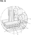
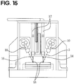
- Fig. 5 to Fig. 15 show various embodiments of the apparatus for manufacturing a solar cell module of the present invention.
- the worktable 7 on which a solar cell 1 is loaded may be mounted on movable mean 8 (e.g., linear stepping motor) capable of precisely reciprocating the worktable in a predetermined speed in one or both directions, and therefore, the solar cell 1 mounted thereon can be moved in the predetermined speed, whereby the tabbing process can be performed while the contact portion is precisely scanned.
- the worktable 7 may include at its upper portion a heating means such as a heating plate (e.g., vacuum heating plate) capable of heating the solar cell mounted thereon. Accordingly, after the solar cell 1 is mounted on the heating mean, the tabbing process can be performed while the solar cell is heated, so that a thermal loss phenomenon due to the high thermal conductivity of the crystal silicone solar cell can be prevented.
- the kind of the compressing device is not specially limited, as long as it is configured to apply appropriate pressure to the metal electrode so that it is homogeneously and closely compressed onto the solar cell.
- the compressing device may comprise a shaft 9 capable of moving up and down; and a probe pin 3 or a pressurizing plate 4 connected with the terminal portion of the shaft 9.
- the compressing device may be connected to a cylinder capable of being moved upward and downward, and the shaft 9 may have a buffer spring for effective compression process.
- the compressing device may comprise a plurality of probe pins 3 arranged at regular intervals as indicated in Fig. 3 , and the intervals between probe pins may be 2 mm to 10 mm, preferably 4 mm to 6 mm.
- the interval between probe pins can freely controlled in order to accomplish uniform and close contact between the metal electrode and the solar cell.
- a laser may be irradiated from lateral upper side with respect to a contact portion of the metal electrode and the solar cell, and the irradiation angle may be controlled with a range from 0 to 90 degrees, and preferably about 45 degrees.
- the probe pin is made of laser-permeable ceramic as described later, the irradiation angle may be controlled so that a laser may be irradiated from the upper side perpendicular to the width-wise direction of the electrode in the contact portion of the electrode and the solar cell.
- the structure of the pressurizing plate 4 used herein is not specially limited, and it may have a bar shape and flat board shape.
- the probe pin or the pressurizing plate may be made of a laser permeable ceramic.
- the term ⁇ laser permeable ceramic ⁇ used herein refers to a heat-resistant transparent material through which a laser may permeate, and examples of the laser permeable ceramic comprises glass, quartz or zirconia.
- an example of the zirconia includes crystal zirconia having a melting point of about 2,000°C to 3,000°C, and more preferably zirconia having monoclinic crystal structure, tetragonal crystal structure or cubic crystal structure.
- the zirconia having a cubic crystal structure is preferable, since it has an excellent heat-resistance, but it is not limited thereto.
- the compressing device may be prevented from being damaged, and laser may be radiated directly to the compressing device. Therefore, the irradiation direction and angle can be freely controlled, and it is possible that a laser is irradiated in the same vertical plane with the contact portion.
- the probe pin is made of zirconia
- the pressurizing plate is made of glass or quartz.
- the probe pin 3 or the pressurizing plate 4 may comprise thereon a coating layer containing fluorine compound.
- a coating layer containing fluorine compound By comprising the coating layer, a lowering of the tabbing efficiency due to contamination after a long period of using may be prevented.
- the kinds of the fluorine compound is not specially limited, it may comprise F 2 or CF 4 .
- surface treating methods or a thickness of the coating layer is not specially limited, and they are appropriately controlled considering the tabbing efficiency.
- various surface treatment methods other than the method using the fluorine compound may be applied in order to prevent the contamination problems.
- the compressing device (probe pin or pressurizing plate) may be configured so as to be separated from a frame and replaced. Therefore, the compressing device can be replaced by periods.
- the compressing device may comprise a compressing roll 13, or an air-nozzle 14 capable of spraying compressed air to the contact portion of the metal electrode and the solar cell.
- the compressing roll 13 or air-nozzle 14 may be connected to a shaft 9 capable of moving up and down, or the compressing roll 13 or the air-nozzle 14 may be fixed at a predetermined height.
- the air-nozzle 14 may comprise a micro-air-hole having a diameter of about 0.5 mm to about 2 mm, and may be installed about 1 mm to about 2 mm away from the metal electrode.
- the air nozzle is configured so as to spray a heated compressed air (hot air)
- hot air there is advantage in that it can compensate a heat loss due to a high heat conductivity of the silicone solar cell, and thereby more efficient tabbing process is possible.
- the temperature of the hot air may be 150 °C to 250 °C , but it can be freely controlled considering the efficiency of the process.
- the compressing device may comprise a plurality of compressing rolls or air-nozzles.
- the compressing device may comprise a pair of compressing rolls 13 or a pair of air-nozzles 14 that are symmetrically installed with respect to a portion onto which a laser is radiated; and a laser irradiation device 10 (e.g., laser head) capable of irradiating a laser onto a electrode portion between the compressing rolls 13 or air-nozzles 14 from the upper side perpendicular to the width-wise direction of the metal electrode.
- a laser irradiation device 10 e.g., laser head
- the compressing roll 13 or air-nozzles 14 may be installed in a support frame 15 built in H shaped frame so as to be symmetrical to each other according to tabbing direction (lengthwise direction of the metal electrode), and laser irradiation device 10 may be installed so as to irradiate a metal electrode between the compressing rolls 13 or the air-nozzles 14 with a laser 5. Therefore, contamination of the electrode parts and damage of the compressing device due to a laser may be prevented.
- the compressing means compressing rolls or air nozzles
- the laser irradiation device that are installed integrally may be comprised in the apparatus of the present invention so as to be movable according to the tabbing direction.
- the compressing device and the laser irradiation device may be fixed in the apparatus.
- the interval of the rolls or nozzles may be 2 mm to 10 mm, preferably 3 mm to 10 mm, and more preferably 4 mm to 6 mm, but it is not limited thereto.
- the compressing device may comprise a plurality of air nozzles 14 so as to pressurize the whole contact portion of the solar cell and the metal electrode simultaneously.
- the details concerning the air nozzle is same as described above.
- the kind of the laser irradiation device included in the tabbing apparatus of the present invention is not specifically limited.
- the laser irradiation devices such as a fiber diode laser, a ruby laser (Cr 3+ :Al 2 O 3 ), YAG laser (Nd 3+ :Y 3 Al 5 O 12 ), phosphate glass laser, silicate glass laser or YLF (Nd 3+ :LiYF 4 ) may be used.
- the fiber diode laser may be preferably used.
- the laser irradiation device may be configured to include a focusing head 11, an optical fiber and a laser source.
- Such laser irradiation device may be installed in the tabbing apparatus with clamping jig by H shaped frame as indicated in Fig. 5 , and it may be installed in the upper side perpendicular to the widthwise direction of the contact portion of the metal electrode and the solar cell.
- the structure of the apparatus is not specially limited, as long as it is installed so that a laser is irradiated from the upper side perpendicular to the width wise direction of the metal electrode.
- two laser irradiation devices may be respectively equipped on the left and right sides of the worktable in the apparatus of the present invention, and they may be configured to be movable in one or both directions. Further, if necessary, two or more laser irradiation devices may be used, so that the apparatus is configured to simultaneously irradiate the total length of the metal electrodes with a laser.
Landscapes
- Photovoltaic Devices (AREA)
- Laser Beam Processing (AREA)
Description
- The present invention relates to a method for manufacturing a solar cell module and an apparatus therefor.
- Recently, due to problems of environmental pollution and fossil energy depletion in the earth, the development of eco-friendly alternative energy sources and the diversification of future energy sources have appeared as international issues. Under the circumstances, a solar cell has been spotlighted as a future influential alternative energy source, and a continuous drop in the price of the solar cell has caused a world market size related to the solar cell to be rapidly increased.
- A solar cell module, which is an essential element in a solar photovoltaic power generation system, has advantages in that a lifetime of about 20 years or more so that it may be semi-permanently used, and a large-sized solar cell module as well as a small-sized solar cell module can be freely manufactured depending on installation locations and scales. In a solar cell module, a thermal bonding process by which solar cells are modularized by being connected to one another in series via power lines, i.e., metal electrodes(ribbons), is referred to as a tabbing or soldering process. A conventional tabbing process is performed in such a manner that a bonding portion between a metal electrode (or ribbon) and a solar cell is heated using a halogen infrared lamp (IR tabbing process) or manually welded by a worker. However, the aforementioned methods, particularly, the IR tabbing process has a problem in that a zone directly irradiated by the infrared lamp is excessively larger than a bonding area required for the tabbing process so that a solar cell module may be more likely to be damaged during the tabbing process. Typically, a solar cell such as a crystal silicon solar cell has a multi-layered structure (e.g., including A1 coating layer, Si wafer layer and SiN3Ar coating layer) of which the layers are made of different materials. Accordingly, if a directly-irradiated zone is excessively large as described above in the same manner as the conventional IR tabbing process, differences in thermal expansion/contraction behaviors of the materials for the respective layers of the solar cell upon application of thermal energy thereto cause the solar cell module to be bent up to 3 mm, resulting in defects in the solar cell module, such as a crack, breakage, damage or warping.
- These problems hinder the recently required thinness of solar cells. That is, most of the crystal silicon solar cells, which have been conventionally used, generally have a thickness of about 230 µm, but solar cells even having a thickness of about 50 µm have the substantially same efficiency. Accordingly, since the silicon depletion and the increasing manufacturing cost caused by the increasing demand for silicon have been recently raised, recently, the requirements for thinness of solar cells are increased. As such, the problems of the conventional tabbing process would be more raised, and therefore, a new tabbing method has been required in which a direct radiation zone in a solar cell is minimized during the tabbing process, thereby preventing the solar cell from being damaged due to different physical properties (thermal expansion/contraction coefficient, and the like) of materials of a multi-layered structure, the bonding property and boding uniformity between the solar cell and electrodes can be improved, and the manufacturing efficiency can be increased.
- Document
JP 60 202968 A - The present invention is conceived to solve the aforementioned problems in the prior art. An object of the present invention is to provide a method and apparatus for manufacturing a solar cell module, in which a bonding process between a metal electrode and the solar cell is performed by local heating with a laser, so that a fraction defective in the tabbing process can be reduced, the bonding strength and bonding uniformity can be improved, and the processing time can be reduced, thereby improving the productivity.
- According to an aspect of the present invention for achieving the objects, there is provided a method for manufacturing a solar cell module, according to
claim 1. - According to another aspect of the present invention for achieving the objects, there is provided an apparatus for manufacturing a solar cell module, accodring to claim 7.
- According to the present invention, a tabbing process of a solar cell and a metal electrode is performed by local heating with a laser, which can localize a heating zone to a minimally required area, so that a direct radiation zone to which thermal energy is directly radiated can be minimized during the process. Therefore, according to the present invention, there are advantages in that it is possible to reduce a fraction defective (generation of crack, breakage and damage) caused by different physical properties (thermal expansion/contraction coefficient) between materials of the solar cell configured to have a multi-layered structure, to provide the high and uniform bonding strength to the contact portion, and to reduce the processing time, thereby improving the production efficiency.
-
-
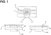
Fig. 1 is a schematic view illustrating a process through which metal electrodes are compressed onto a solar cell in accordance with one embodiment of the present invention. -
Fig. 2 is a schematic view illustrating a state where a tabbing process is performed using irradiation with a laser in accordance with the embodiment of the present invention. -
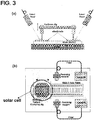
Fig. 3 is a schematic view illustrating a state where a tabbing process is performed using irradiation with a laser in accordance with another embodiment of the present invention. -
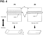
Fig. 4 is a schematic view illustrating deformation states of solar cells and a difference in HAZ during both a conventional tabbing process using an infrared lamp and the tabbing process according to the present invention. -
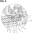
Fig. 5 to 15 are drawings indicating various embodiments of the apparatus for manufacturing a solar cell module. - The present invention is related to a method for manufacturing a solar cell module, which comprises: a first step of compressing a metal electrode onto a solar cell; and a second step of performing a tabbing process by irradiating a contact portion of the metal electrode and the solar cell with a laser.
- Hereinafter, the method according to the present invention will be described in detail.
- The first step of the present invention is a step of preparing a tabbing process by compressing a metal electrode onto a solar cell. At this time, the kind of solar cell onto which the metal electrode is compressed is not specifically limited, but a crystal silicon solar cell, such as a single crystal silicon solar cell and a polycrystalline silicone solar cell, may be included in an example of the solar cell.
- The method of the present invention may be effectively applied to a thinned solar cell, since a direct radiation zone and a mechanical stress (or thermal stress) applied to the thin solar cell can be minimized. Therefore, the solar cell applied to the present method may have a thickness ranging from 80 µm to 200 µm. If the thickness is less than 80 µm, it is apprehended that the efficiency of the solar cell is decreased. If the thickness is more than 200 µm, it is apprehended that economical efficiency is lowered.
- The kind of the metal electrode (ribbon) to be compressed in the first step of the present invention is not specifically limited, but all metal electrodes which have been conventionally used in a solar cell field may be included in an example of the metal electrode. A Cu electrode may be a representative example of the metal electrode as described above. Generally, there is a low melting point alloy layer (e.g., an alloy layer of Cu, Sn and Al), whose melting point is about 260°C, on upper and lower portions of the Cu electrode as described above. Conventionally, the metal electrode as described above has a width ranging from 1.5 mm to 2.5 mm and a thickness ranging from 80 µm to 300 µm. However, the present invention is not limited thereto, but various metal electrodes may be used. If the metal electrodes are excessively thin, there is an advantage in that the power or scanning speed of a laser used in tabbing can be reduced, but the efficiency of a solar cell module may be decreased due to the increase of the electrode resistance. Therefore, it is preferable to select the electrode having an appropriate thickness according to applications.
- The metal electrode is compressed onto the solar cell in the first step of the present invention, at this time it is preferable that uniform pressure is applied with respect to the whole contact portions of the metal electrode and the solar cells. If uniform compression is not carried out, it is apprehended that the the metal electrode is not uniformly bonded to the solar cell, and thereby efficiency of the solar cell module is lowered due to electrical loss. In the present invention, for instance, the compression process may be carried out by using a compression device comprising probe pin, pressurizing plate, compressing roll or air-nozzle. However, the above description is no more than an example of the present invention, and the means for compression is not specifically limited only if the metal electrodes can be uniformly and closely compressed onto the solar cell.
- Further, it is preferable that the metal electrodes be simultaneously compressed on front and rear surfaces of the solar cell in the first step of the present invention. That is, as shown in
Fig. 1 , themetal electrodes 2 are tabbed on the left and right sides of the front surface of thesolar cell 1, respectively. At this time, the metal electrodes are bonded onto the left and right sides of the rear surface of the solar cell as well as the left and right sides of the front surface of the solar cell. Accordingly, all the four metal electrodes are simultaneously compressed onto the left and right sides of the front and rear surfaces of the single solar cell in accordance with the present invention, respectively, and then, left and right sides thereof are irradiated with a laser, thereby performing the tabbing process. If such a process is performed, the heat to be generated by the laser applied to the upper portion is conducted to the lower portion, so that the tabbing process can be performed in the upper and lower portions simultaneously. It is preferable in the first step of the present invention that the compression of the metal electrodes is performed at a pressure of 0.3 N/m to 0.6 N/m. The contact of the metal electrodes may be deteriorated if the pressure is smaller than 0.3 N/m, whereas the excessive pressure may damage the solar cell if the pressure is larger than 0.6 N/m. - In the second step of the present invention, the tabbing process is performed by irradiating the contact portions of the solar cell and the metal electrode with a laser. A process of performing the second step of the present invention will be specifically described with reference to the accompanying drawings.
Fig. 2 of the accompanying drawings is a schematic view showing a state where the tabbing process is performed by irradiation with a laser according to one embodiment of the present invention. As shown inFig. 2 , in the second step, the tabbing process is performed by locally heating the contact portions of thesolar cell 1 and the metal electrodes 2-1 and 2-2 by alaser 5. Thelaser 5 radiated in the second step is a defocused laser. If the focused laser is used to perform the tabbing process of the present invention, the energy applied to the contact portion is excessively high, so that the degradation such as deformation of the solar cell may be generated. - It is preferable that in the second step of the present invention, a
defocused core size 6, in which the defocused laser as described above is diffused in the contact portion, is controlled to be identical with the width of the metal electrodes 2-1 and 2-2. Such control can cause a direct heating zone with a laser to be localized to a minimal area required to perform the tabbing process. If the defocused core size is smaller than the width of the metal electrode, it may be difficult to uniformly heat the contact portion. If the defocused core size is larger than the width of the metal electrode, the front surface of the solar cell other than the contact portion is directly irradiated with the laser, so that the solar cell may be damaged. Since the width of the metal electrode ranges from about 1.5 to 2.5 mm as described above, the defocused core size may be controlled to range from 1.5 to 2.5 mm in the present invention. However, the above description is no more than one example, and the specific values may not be specifically limited thereto in the present invention only if the defocused core size is controlled to be identical with the width of the metal electrode. - Further, the laser used in the second step of the present invention has a wavelength of 700 nm to 1000 nm, and more preferably 800 nm to 900 nm. Further, the maximum power of the laser ranges from 20 W to 150 W, and more preferably from 90 W to 110 W. If the wavelength of the irradiation laser is smaller than 700 nm, there is a problem in relation to the bonding strength and the like under a fast tabbing speed, so that the fraction defective may increase. Further, if the wavelength is larger than 1000 nm, the tabbing process may not be performed smoothly. However, the wavelength and maximum power of the laser as described above is no more than an example of the present invention, and therefore, they may be appropriately adjusted depending on the specification of the solar cell and/or the thickness of the metal electrode, which are applied in the tabbing process. For example, if the method of the present invention is performed using a 5 inch solar cell and metal electrodes having a thickness of 150 µm, it is preferable that the wavelength of the laser is about 808 nm and the maximum power is about 60 W.
- In the present invention, it is preferable that the laser be radiated from the upper side perpendicular to the widthwise direction of the electrode in the contact portion of the electrode and the solar cell. The term widthwise direction refers to a direction perpendicular to a lengthwise direction of the electrode constituting the contact portion. That is, in the present invention, it is preferable that the laser is radiated in the same vertical plane with the contact portion line, and such control of the radiation direction can be accomplished by using a compressing device comprising a laser-permeable ceramic, compressing roll or air-nozzle as described later. In the present invention, the term ┌same vertical plane with the contact portion lined┘ refers to a imaginary plane which is formed upward perpendicular to the surface of the solar cell according to the contact portion line (the lengthwise direction of the electrode). Since the laser is radiated in the same vertical plane with the contact portion line, there is advantage in that the irradiation angle of the laser may be freely controlled, and focusing of the laser may be easily accomplished since the laser beam is refracted in the same line with the contact portion.
- In the present invention, the irradiation angle of the laser in the second step of the present invention may be controlled to range from 0 to 90 degrees, preferably not more than 40 degrees, more preferably not more than 20 degrees, and most preferably 10 degrees. The ┌irradiation angle┘ used herein refers to an angle between an irradiated laser and a normal line that is formed with respect to the contact portion line on which the laser is radiated. In the present invention, according to a solar cell and/or a metal electrode, the irradiation angle is controlled within the above range so that an average reflexibility may be minimized. In the present invention, as described above, since the irradiation angle and the refractive direction of the laser are optimized, and thereby the tabbing process may be carried out with minimized energy loss. Therefore, in the present invention, electrode arranging speed per unit time can be increased. However, the above description is no more than an example of the present invention, and therefore, the irradiation angle may be adjusted, considering the size of the solar cell, the intervals of the tabbed metal electrodes, the possibility of damaging apparatus (ex. focusing head of the laser device) due to the refracted laser, and the like
- As shown in
Fig. 2 , according to the present invention, the second step may be performed while the solar cell or the laser is moved in a tabbing direction. The term ┌tabbing direction┘ used in the present invention refers to a lengthwise direction of the metal electrode positioned on the solar cell, wherein the movement may cause the laser to sequentially scan the contact portions and heat them. At this time, the movement may be performed by moving a worktable on which the solar cell is mounted, or the irradiation laser itself. Here, the moving speed may be adjusted considering the tabbing efficiency relative to laser irradiation time depending on the power of laser, the defocused core size, the kind of the solar cell and/or the metal electrodes, and the like, and is not specifically limited. For example, if the metal electrode having a width of about 2 mm and a thickness of about 150 µm, and the defocused laser having a power of 60 W are used to perform the tabbing process, the scanning speed may be not less than about 10 mm/sec, preferably about 25 mm/sec to 125 mm/sec, more preferably about 62.5 mm/sec to 125 mm/sec. However, the above description is no more than an example of the present invention, and without performing the moving process required in case of using a spot beam, one or more laser irradiation devices (line beam) may be used to simultaneously heat the total length of the metal electrodes to be tabbed in the present invention. Thus, only the single irradiation makes it possible to perform the tabbing process. The term ┌spot beam┘ used in the present invention refers to a case where a device is configured to irradiate a predetermined dot region of the metal electrode on the solar cell with a laser, while the term ┌line beam┘ refers to a case where a device is configured to irradiate the total region of the metal electrode on the contact portion with a laser simultaneously. In a case where such a line beam heats the total length of the metal electrode simultaneously at a time to perform the tabbing process, the process time per the single solar cell can be reduced to be about 1 to 2 seconds. - In the present invention, the second step is performed while the lower portion of the solar cell is heated at a predetermined temperature. At this time, the heating temperature preferably ranges from 110 °C to 180 °C . That is, since the crystalline silicon solar cell or the like has high thermal conductivity, the heat absorbed in the electrode contact portion may not be used in the tabbing process but may quickly vanish. Therefore, the tabbing process is performed while the lower portion of the solar cell is heated with an appropriate heating means, so that the efficiency of the tabbing process can be further improved. Further, when the metal electrodes are simultaneously compressed onto the front and the rear surfaces of the solar cell to perform the tabbing process as described above, the thermal conduction due to the heat input by the laser alone may not satisfy the energy required for the tabbing process. Therefore, there is an advantage in that the heating process for the lower portion can compensate such insufficient energy. The kind of the heating means and the heating method, which may be used in the present invention, are not specifically limited. For example, there is a method wherein a heating plate is mounted on a worktable onto which the solar cell is loaded, the solar cell is mounted on the heating plate, and then the solar cell is heated by the heating plate while the tabbing process is performed. Further, as shown in
Fig. 3 , it is preferred in the present invention that two laser irradiation devices be provided and the laser be simultaneously radiated in the left and right directions of the solar cell on which the metal electrodes are compressed. Accordingly, the metal electrodes positioned on the left and right sides of the solar cell are simultaneously tabbed by the single process, so that the efficiency of the process can be further improved.Fig. 3 (a) is a side view illustrating a tabbing process performed according to an aspect of the present invention, whileFig. 3 (b) is a plan view illustrating the tabbing process. - According to the present method as described above, the contact portion can be locally heated during the tabbing process, so that the direct radiation zone to the contact portion can be minimized. Therefore, according to the present invention, the defect caused by different thermal expansion/contraction coefficients in the multi-layered solar cell can be prevented, and the process can be quickly and efficiently performed.
Fig. 4 of the accompanying drawings is a view illustrating difference in direct radiation zone (HAZ; Heat Affecting Zone) (the area indicated with dots inFig. 4 ) shown on the solar cells and deformation states of the solar cells in both a conventional tabbing process (Fig. 4 (a) ) using an infrared lamp and a tabbing process (Fig. 4 (b) ) according to one embodiment of the present invention. As shown inFig. 4 , the present invention makes it possible to remarkably reduce the direct radiation zone as compared with the conventional method, so that the defect caused by the non-uniform expansion/contraction of the multi-layered solar cell can be effectively prevented during the process or during cooling. - The present invention is related to an apparatus for manufacturing a solar cell module, which comprises: a worktable on which a solar cell is loaded; a compressing device capable of compressing a metal electrode on the solar cell loaded on the worktable; and a laser irradiation device capable of irradiating a contact portion of the solar cell and the metal electrode compressed by the compressing device with a laser.
-
Fig. 5 to Fig. 15 show various embodiments of the apparatus for manufacturing a solar cell module of the present invention. - The
worktable 7 on which asolar cell 1 is loaded may be mounted on movable mean 8 (e.g., linear stepping motor) capable of precisely reciprocating the worktable in a predetermined speed in one or both directions, and therefore, thesolar cell 1 mounted thereon can be moved in the predetermined speed, whereby the tabbing process can be performed while the contact portion is precisely scanned. Further, theworktable 7 may include at its upper portion a heating means such as a heating plate (e.g., vacuum heating plate) capable of heating the solar cell mounted thereon. Accordingly, after thesolar cell 1 is mounted on the heating mean, the tabbing process can be performed while the solar cell is heated, so that a thermal loss phenomenon due to the high thermal conductivity of the crystal silicone solar cell can be prevented. - In the present invention, the kind of the compressing device is not specially limited, as long as it is configured to apply appropriate pressure to the metal electrode so that it is homogeneously and closely compressed onto the solar cell.
- In one embodiment of the present invention, as shown in
Fig. 5 orFig. 6 , the compressing device may comprise ashaft 9 capable of moving up and down; and aprobe pin 3 or a pressurizing plate 4 connected with the terminal portion of theshaft 9. In one embodiment, the compressing device may be connected to a cylinder capable of being moved upward and downward, and theshaft 9 may have a buffer spring for effective compression process. - In one embodiment of the present invention, from the view point of homogenous and uniform compression, the compressing device may comprise a plurality of probe pins 3 arranged at regular intervals as indicated in
Fig. 3 , and the intervals between probe pins may be 2 mm to 10 mm, preferably 4 mm to 6 mm. However, the above description is no more than an example of the present invention, and therefore, the interval between probe pins can freely controlled in order to accomplish uniform and close contact between the metal electrode and the solar cell. - When the compressing device comprises a plurality of probe pins, a laser may be irradiated from lateral upper side with respect to a contact portion of the metal electrode and the solar cell, and the irradiation angle may be controlled with a range from 0 to 90 degrees, and preferably about 45 degrees. However, the above description is no more than one example of the present invention. For instance, the probe pin is made of laser-permeable ceramic as described later, the irradiation angle may be controlled so that a laser may be irradiated from the upper side perpendicular to the width-wise direction of the electrode in the contact portion of the electrode and the solar cell.
- Also, the structure of the pressurizing plate 4 used herein is not specially limited, and it may have a bar shape and flat board shape.
- In one embodiment, the probe pin or the pressurizing plate may be made of a laser permeable ceramic. The term ┌laser permeable ceramic┘ used herein refers to a heat-resistant transparent material through which a laser may permeate, and examples of the laser permeable ceramic comprises glass, quartz or zirconia. Also, an example of the zirconia includes crystal zirconia having a melting point of about 2,000°C to 3,000°C, and more preferably zirconia having monoclinic crystal structure, tetragonal crystal structure or cubic crystal structure. Among these, the zirconia having a cubic crystal structure is preferable, since it has an excellent heat-resistance, but it is not limited thereto.
- In the present invention, when a laser-permeable ceramic is used, there are several advantages as described below.
- In case when a compressing device made of metal material, if a laser is directly radiated on the compressing device, the metal material is damaged, and thereby uniform compression can not be accomplished. Therefore, the irradiation angle of the laser is limited considering the possibility of the damage of the metal material. This defect becomes more serious when probe pin made of metal material is used, since difference in pressure is generated more easily. Also, when a compressing device is madder of metal material, it is not possible to radiate a laser from the upper side perpendicular to the width-wise direction of the electrode in the contact portion of the electrode and the solar cell, and it should be radiated from lateral side. In that case, the control of the irradiation angle is limited due to constitution of the apparatus. While, if the laser permeable ceramic is used, the compressing device may be prevented from being damaged, and laser may be radiated directly to the compressing device. Therefore, the irradiation direction and angle can be freely controlled, and it is possible that a laser is irradiated in the same vertical plane with the contact portion.
- Therefore, by irradiating a laser with its defocused core size being controlled to be identical with the width of the metal electrodes after forming a uniform contact portion using a
probe pin 3 or a pressurizing plate 4 made of the laser permeable ceramic, uniform and close tabbing from the start point to end point of the contact portion is possible. Also, the thermal damage of the solar cell is prevented, since a laser-irradiating range can be easily limited to the contact portion. Although it is not specially limited, it is preferable that the probe pin is made of zirconia, and the pressurizing plate is made of glass or quartz. - In one embodiment, the
probe pin 3 or the pressurizing plate 4 may comprise thereon a coating layer containing fluorine compound. By comprising the coating layer, a lowering of the tabbing efficiency due to contamination after a long period of using may be prevented. In the present invention, the kinds of the fluorine compound is not specially limited, it may comprise F2 or CF4. At this time, surface treating methods or a thickness of the coating layer is not specially limited, and they are appropriately controlled considering the tabbing efficiency. Also, in the present invention, various surface treatment methods other than the method using the fluorine compound may be applied in order to prevent the contamination problems. Also, in the present invention, the compressing device (probe pin or pressurizing plate) may be configured so as to be separated from a frame and replaced. Therefore, the compressing device can be replaced by periods. - In one embodiment, as indicated in
Fig. 7 to Fig. 12 , the compressing device may comprise a compressingroll 13, or an air-nozzle 14 capable of spraying compressed air to the contact portion of the metal electrode and the solar cell. Also, the compressingroll 13 or air-nozzle 14 may be connected to ashaft 9 capable of moving up and down, or the compressingroll 13 or the air-nozzle 14 may be fixed at a predetermined height. - The air-
nozzle 14 may comprise a micro-air-hole having a diameter of about 0.5 mm to about 2 mm, and may be installed about 1 mm to about 2 mm away from the metal electrode. Specially, if the air nozzle is configured so as to spray a heated compressed air (hot air), there is advantage in that it can compensate a heat loss due to a high heat conductivity of the silicone solar cell, and thereby more efficient tabbing process is possible. At this time, the temperature of the hot air may be 150 °C to 250 °C , but it can be freely controlled considering the efficiency of the process. - In one embodiment, from the view point of more efficient compression and tabbing process, the compressing device may comprise a plurality of compressing rolls or air-nozzles. In this case, the compressing device may comprise a pair of compressing rolls 13 or a pair of air-
nozzles 14 that are symmetrically installed with respect to a portion onto which a laser is radiated; and a laser irradiation device 10 (e.g., laser head) capable of irradiating a laser onto a electrode portion between the compressing rolls 13 or air-nozzles 14 from the upper side perpendicular to the width-wise direction of the metal electrode. In this case, as indicated inFig. 8 ,9 ,11 and12 , the compressingroll 13 or air-nozzles 14 may be installed in asupport frame 15 built in H shaped frame so as to be symmetrical to each other according to tabbing direction (lengthwise direction of the metal electrode), andlaser irradiation device 10 may be installed so as to irradiate a metal electrode between the compressing rolls 13 or the air-nozzles 14 with alaser 5. Therefore, contamination of the electrode parts and damage of the compressing device due to a laser may be prevented. - The compressing means (compressing rolls or air nozzles) and the laser irradiation device that are installed integrally may be comprised in the apparatus of the present invention so as to be movable according to the tabbing direction. However, if the worktable on which a solar cell is mounted is installed so as to be moved, the compressing device and the laser irradiation device may be fixed in the apparatus.
- Also, in case when a pair of compressing rolls or air-nozzles is installed so as to be symmetrical to each other, the interval of the rolls or nozzles may be 2 mm to 10 mm, preferably 3 mm to 10 mm, and more preferably 4 mm to 6 mm, but it is not limited thereto.
- In another embodiment, as indicated in
Fig. 13 to 15 , the compressing device may comprise a plurality ofair nozzles 14 so as to pressurize the whole contact portion of the solar cell and the metal electrode simultaneously. In this case, the details concerning the air nozzle is same as described above. - Further, the kind of the laser irradiation device included in the tabbing apparatus of the present invention is not specifically limited. For example, the laser irradiation devices such as a fiber diode laser, a ruby laser (Cr3+:Al2O3), YAG laser (Nd3+:Y3Al5O12), phosphate glass laser, silicate glass laser or YLF (Nd3+:LiYF4) may be used. In the present invention, from the viewpoint of having an excellent durability enough to be semi-permanently used and a low price, the fiber diode laser may be preferably used. In this case, the laser irradiation device may be configured to include a focusing
head 11, an optical fiber and a laser source. Such laser irradiation device may be installed in the tabbing apparatus with clamping jig by H shaped frame as indicated inFig. 5 , and it may be installed in the upper side perpendicular to the widthwise direction of the contact portion of the metal electrode and the solar cell. However, it is only one example of the present invention, the structure of the apparatus is not specially limited, as long as it is installed so that a laser is irradiated from the upper side perpendicular to the width wise direction of the metal electrode. - Further, two laser irradiation devices may be respectively equipped on the left and right sides of the worktable in the apparatus of the present invention, and they may be configured to be movable in one or both directions. Further, if necessary, two or more laser irradiation devices may be used, so that the apparatus is configured to simultaneously irradiate the total length of the metal electrodes with a laser.
Claims (14)
- A method for manufacturing a solar cell module, comprising:a first step of compressing a metal ribbon electrode onto a solar cell; anda second step of performing a tabbing process by irradiating a contact portion of the metal ribbon electrode and the solar cell with a defocused laser, of which a wavelength is in a range from 700 nm to 1,000 nm and a maximum power is in a range from 20 W to 150 W, the second step being performed with heating a lower portion of the solar cell at a heating temperature of 110°C to 180°C.
- The method as claimed in claim 1, wherein the metal ribbon electrodes are compressed on the front and rear surfaces of the solar cell in the first step.
- The method as claimed in claim 1, wherein a defocused core size, in which the defocused laser is diffused at the contact portion, is controlled to be identical with the width of the metal ribbon electrode.
- The method as claimed in claim 3, wherein the defocused core size ranges from 1.5 mm to 2.5 mm.
- The method as claimed in claim 1, wherein the laser is irradiated from the upper side perpendicular to the widthwise direction of the metal ribbon electrode in the contact portion.
- The method as claimed in claim 1, wherein the irradiation angle of the laser is controlled to be not more than 40°.
- An apparatus for manufacturing a solar cell module, comprising:a worktable, on which a solar cell is loaded, and which comprises at its upper portion a heating means capable of heating the solar cell; a compressing device capable of compressing a metal ribbon electrode onto the solar cell loaded on the work table; anda laser irradiation device capable of irradiating a contact portion of the metal ribbon electrode and the solar cell with a defocused laser, of which a wavelength is in a range from 700 nm to 1,000 nm and a maximum power is in a range from 20 W to 150 W.
- The apparatus as claimed in claim 7, wherein the compressing device comprises a shaft that is capable of moving up and down; and a probe pin or a pressurizing plate that is connected with a terminal portion of the shaft.
- The apparatus as claimed in claim 8, wherein the probe pin or the pressurizing plate is made of a laser permeable ceramic.
- The apparatus as claimed in claim 9, wherein the ceramic comprises glass, quartz or zirconia.
- The apparatus as claimed in claim 7, wherein the compressing device comprises a compressing roll; or an air-nozzle that is capable of spraying compressed air onto a contact portion of the metal ribbon electrode and the solar cell.
- The apparatus as claimed in claim 11, wherein the compressing device comprises a pair of compressing rolls or a pair of air-nozzles that are symmetrically installed with respect to a portion onto which the defocused laser is radiated; and the laser irradiation device that is capable of irradiating the defocused a laser onto a portion between the compressing rolls or air-nozzles from the upper side perpendicular to the widthwise direction of the metal ribbon electrode.
- The apparatus as claimed in claim 12, wherein intervals between the compressing rolls or air-nozzles is 2 mm to 10 mm.
- The apparatus as claimed in claim 7, wherein the compressing device comprises a plurality of air-nozzles capable of simultaneously pressurizing the whole contact portion of the metal ribbon electrode and the solar cell.
Applications Claiming Priority (2)
| Application Number | Priority Date | Filing Date | Title |
|---|---|---|---|
| KR20070124320 | 2007-12-03 | ||
| PCT/KR2008/006792 WO2009072760A2 (en) | 2007-12-03 | 2008-11-18 | Methods for manufacturing solar cell module and apparatus for manufacturing the same |
Publications (3)
| Publication Number | Publication Date |
|---|---|
| EP2218109A2 EP2218109A2 (en) | 2010-08-18 |
| EP2218109A4 EP2218109A4 (en) | 2012-07-11 |
| EP2218109B1 true EP2218109B1 (en) | 2017-01-04 |
Family
ID=40718325
Family Applications (1)
| Application Number | Title | Priority Date | Filing Date |
|---|---|---|---|
| EP08856189.9A Not-in-force EP2218109B1 (en) | 2007-12-03 | 2008-11-18 | Methods for manufacturing solar cell module and apparatus for manufacturing the same |
Country Status (5)
| Country | Link |
|---|---|
| US (1) | US8674261B2 (en) |
| EP (1) | EP2218109B1 (en) |
| KR (2) | KR100912037B1 (en) |
| CN (1) | CN101884114B (en) |
| WO (1) | WO2009072760A2 (en) |
Families Citing this family (21)
| Publication number | Priority date | Publication date | Assignee | Title |
|---|---|---|---|---|
| DE102009041810A1 (en) * | 2009-09-18 | 2011-03-24 | Wolf Produktionssysteme Gmbh | Carrier element for transporting a circuit carrier |
| KR101206608B1 (en) * | 2009-11-17 | 2012-11-29 | (주)엘지하우시스 | Laser sealing apparatus for glass substrate |
| ATE539452T1 (en) * | 2009-12-22 | 2012-01-15 | Kioto Photovoltaics Gmbh | DEVICE FOR FIXING CONDUCTOR TRACKS ON A SOLAR CELL |
| US8561878B2 (en) * | 2010-09-27 | 2013-10-22 | Banyan Energy, Inc. | Linear cell stringing |
| TWI423458B (en) * | 2010-12-08 | 2014-01-11 | Ritek Corp | Method of tabbing and stringing solar cells |
| EP2634822A1 (en) * | 2012-02-29 | 2013-09-04 | IMA Automation Berlin GmbH | Device for fixing the position of a solder connector to a solar cell |
| US9757820B2 (en) * | 2012-05-24 | 2017-09-12 | GM Global Technology Operations LLC | Welding fixture for joining bar-wound stator conductors |
| EP2804224A1 (en) | 2013-05-13 | 2014-11-19 | Fraunhofer Gesellschaft zur Förderung der angewandten Forschung e.V. | Method for producing a photovoltaic module |
| CN104183666B (en) | 2013-05-26 | 2017-06-16 | 苏州易益新能源科技有限公司 | A kind of laser welding couples the method for crystal silicon solar energy battery |
| JP6535529B2 (en) * | 2015-07-08 | 2019-06-26 | 不二越機械工業株式会社 | Dressing apparatus and dressing method for polishing cloth of double-side polishing apparatus |
| KR20170026682A (en) * | 2015-08-26 | 2017-03-09 | 주식회사 제우스 | Solar cell tabbing apparatus |
| CN107914086A (en) * | 2017-12-22 | 2018-04-17 | 君泰创新(北京)科技有限公司 | A kind of solar cell busbar welder |
| CN109877454B (en) * | 2019-04-11 | 2021-02-09 | 武汉华工激光工程有限责任公司 | Laser welding method for thin-film solar cell electrode |
| CN111906440A (en) * | 2020-07-28 | 2020-11-10 | 东莞市中麒光电技术有限公司 | Preparation method of display screen module |
| JP7315523B2 (en) * | 2020-12-04 | 2023-07-26 | 矢崎総業株式会社 | Terminal fixing method |
| CN113199108A (en) * | 2021-06-12 | 2021-08-03 | 广东省闪耀科技开发有限公司 | Electronic fixing press welder |
| CN113199109A (en) * | 2021-06-12 | 2021-08-03 | 广东省闪耀科技开发有限公司 | Electronic movable press welder |
| CN115548160B (en) * | 2021-06-30 | 2025-08-05 | 晶科能源股份有限公司 | Photovoltaic cell string repair device and repair method |
| CN114850216B (en) * | 2022-07-04 | 2022-10-04 | 太原理工大学 | A method for preparing bimetallic composite panels by electronically controlled micro-explosive molding |
| CN118738210B (en) * | 2024-06-21 | 2025-11-11 | 广东科隆威智能装备股份有限公司 | Laser-induced passivation machine and passivation method |
| CN118588815B (en) * | 2024-08-07 | 2024-10-01 | 绵阳炘皓新能源科技有限公司 | A preparation method and battery for improving hidden cracks in TOPCon battery grid lines |
Family Cites Families (27)
| Publication number | Priority date | Publication date | Assignee | Title |
|---|---|---|---|---|
| JPS604270A (en) * | 1983-06-22 | 1985-01-10 | Hitachi Ltd | Manufacture of solar battery |
| JPS60202968A (en) * | 1984-03-28 | 1985-10-14 | Hitachi Ltd | Electrode connecting device of solar battery cell |
| JPS63115671A (en) * | 1986-10-31 | 1988-05-20 | Nippei Toyama Corp | Soldering method for covered wire |
| US4959522A (en) * | 1990-01-12 | 1990-09-25 | Chrysler Corporation | Transparent pressure foot |
| JPH0491493A (en) | 1990-08-01 | 1992-03-24 | Nippon Mektron Ltd | Laser soldering and device therefor |
| JPH09327781A (en) * | 1996-06-12 | 1997-12-22 | Ishikawajima Harima Heavy Ind Co Ltd | Laser light irradiation head positioning device |
| US5823417A (en) * | 1996-07-09 | 1998-10-20 | Johnson; Jeffrey Don | Laser pressure foot |
| US6333483B1 (en) * | 1997-04-04 | 2001-12-25 | Taiyo Yuden Co., Ltd. | Method of manufacturing circuit modules |
| US6239352B1 (en) | 1999-03-30 | 2001-05-29 | Daniel Luch | Substrate and collector grid structures for electrically interconnecting photovoltaic arrays and process of manufacture of such arrays |
| JP2001071171A (en) * | 1999-08-31 | 2001-03-21 | Canon Inc | Metal bonding equipment |
| JP3394750B2 (en) * | 2000-10-02 | 2003-04-07 | ファナック株式会社 | Work pressing device |
| US6395972B1 (en) * | 2000-11-09 | 2002-05-28 | Trw Inc. | Method of solar cell external interconnection and solar cell panel made thereby |
| JP2002207119A (en) * | 2001-01-05 | 2002-07-26 | Teijin Ltd | Polyester film for polarizing plate release |
| US6524880B2 (en) * | 2001-04-23 | 2003-02-25 | Samsung Sdi Co., Ltd. | Solar cell and method for fabricating the same |
| US6803538B2 (en) * | 2001-08-31 | 2004-10-12 | Honda Canada Inc. | Laser welding system |
| NL1020627C2 (en) * | 2002-05-21 | 2003-11-24 | Otb Group Bv | Method and tab station for applying tabs to a solar cell as well as a method and device for manufacturing a solar panel. |
| DE10226517C1 (en) * | 2002-06-14 | 2003-10-30 | Dreistern Werk Maschinenbau Gmbh & Co Kg | Hollow profile manufacturing method has metal band welded across open side of open profile formed from metal band of varying width |
| JP2004134654A (en) * | 2002-10-11 | 2004-04-30 | Sharp Corp | Method of manufacturing solar cell module |
| DE50200203D1 (en) * | 2002-10-18 | 2004-02-12 | Dreistern Werk Maschinenbau Gmbh & Co Kg | Stationary welding device and method for longitudinal welding of profiles |
| US7649141B2 (en) * | 2003-06-30 | 2010-01-19 | Advent Solar, Inc. | Emitter wrap-through back contact solar cells on thin silicon wafers |
| EP1518664A1 (en) * | 2003-09-20 | 2005-03-30 | Leister Process Technologies | Process and apparatus for joining components by laser radiation |
| DE102004009950A1 (en) * | 2004-03-01 | 2005-09-22 | Innolas Gmbh | Laser machining system has sheet metal workpieces held flat by creation of a cushion of compressed air |
| WO2006000834A1 (en) * | 2004-06-24 | 2006-01-05 | Heliodynamics Limited | Solar energy collection systems |
| US7538295B2 (en) * | 2005-04-21 | 2009-05-26 | Hewlett-Packard Development Company, L.P. | Laser welding system |
| US20060266473A1 (en) * | 2005-05-26 | 2006-11-30 | Kimberly-Clark Worldwide, Inc. | Bonding by induced high-rate of shear deformation |
| DE102006014068A1 (en) * | 2006-03-27 | 2007-10-04 | Precitec Kg | Apparatus and method for clamping sheet metal components |
| CN101678255A (en) * | 2007-05-31 | 2010-03-24 | 东丽株式会社 | Nonwoven fabric for cylindrical bag filter, process for producing the same, and cylindrical bag filter therefrom |
-
2008
- 2008-04-17 KR KR1020080035653A patent/KR100912037B1/en not_active Expired - Fee Related
- 2008-11-11 KR KR1020080111743A patent/KR101206713B1/en not_active Expired - Fee Related
- 2008-11-18 EP EP08856189.9A patent/EP2218109B1/en not_active Not-in-force
- 2008-11-18 WO PCT/KR2008/006792 patent/WO2009072760A2/en not_active Ceased
- 2008-11-18 US US12/745,225 patent/US8674261B2/en not_active Expired - Fee Related
- 2008-11-18 CN CN2008801191047A patent/CN101884114B/en not_active Expired - Fee Related
Non-Patent Citations (1)
| Title |
|---|
| None * |
Also Published As
| Publication number | Publication date |
|---|---|
| CN101884114A (en) | 2010-11-10 |
| CN101884114B (en) | 2013-07-24 |
| EP2218109A4 (en) | 2012-07-11 |
| KR20090057865A (en) | 2009-06-08 |
| US20110031225A1 (en) | 2011-02-10 |
| WO2009072760A2 (en) | 2009-06-11 |
| US8674261B2 (en) | 2014-03-18 |
| KR100912037B1 (en) | 2009-08-12 |
| KR20090057891A (en) | 2009-06-08 |
| WO2009072760A3 (en) | 2009-08-06 |
| EP2218109A2 (en) | 2010-08-18 |
| KR101206713B1 (en) | 2012-11-29 |
Similar Documents
| Publication | Publication Date | Title |
|---|---|---|
| US8674261B2 (en) | Method for manufacturing a solar cell module by laser bonding | |
| US12611721B2 (en) | Laser reflow apparatus and laser reflow method | |
| CN110326096B (en) | Laser reflow soldering equipment | |
| US20120131959A1 (en) | Laser sealing device for glass substrates | |
| KR102022600B1 (en) | Laser reflow apparatus | |
| CN109361138B (en) | Slab laser gain medium packaging method | |
| CN1085012A (en) | Be used for removing the method and apparatus of electronic component from substrate | |
| CN102341211A (en) | Method of working thin layer on work and thin layor working apparatus | |
| US10138162B2 (en) | Method and device for bonding workpieces each produced from glass substrate or quartz substrate | |
| KR102199450B1 (en) | Laser pressure head module of laser reflow equipment | |
| KR102217812B1 (en) | Producing device of mask integrated frame | |
| EP2147899A1 (en) | Method for processing terminal in bonded substrate | |
| JPH10277772A (en) | Substrate beam processing equipment | |
| CN102442769A (en) | Glass substrate chamfering method and device | |
| JP2011044598A (en) | Device and method for connection of solar cell substrate | |
| CN114436519A (en) | Large-breadth glass laser high-speed cutting and sheet breaking method and device | |
| KR101182879B1 (en) | Apparatus and Process of Sola Cell Ribbon Soldering | |
| JP2010087041A (en) | Method of removing thin film by laser beam, and method of manufacturing thin-film solar cell panel | |
| CN116801685A (en) | Laser repairing method and device for perovskite layer of solar cell | |
| JP4616441B2 (en) | Solar cell manufacturing method | |
| KR20200129437A (en) | Laser reflow method of laser reflow apparatus | |
| KR102174930B1 (en) | Laser pressure head module of laser reflow equipment | |
| KR102236541B1 (en) | Producing method of mask, producing method of template for supporting mask and producing method of mask integrated frame | |
| KR101206553B1 (en) | Apparatus for manufacturing a solar cell module | |
| KR101818918B1 (en) | Laser reflow method and substrate structure thereby |
Legal Events
| Date | Code | Title | Description |
|---|---|---|---|
| PUAI | Public reference made under article 153(3) epc to a published international application that has entered the european phase |
Free format text: ORIGINAL CODE: 0009012 |
|
| 17P | Request for examination filed |
Effective date: 20100601 |
|
| AK | Designated contracting states |
Kind code of ref document: A2 Designated state(s): AT BE BG CH CY CZ DE DK EE ES FI FR GB GR HR HU IE IS IT LI LT LU LV MC MT NL NO PL PT RO SE SI SK TR |
|
| AX | Request for extension of the european patent |
Extension state: AL BA MK RS |
|
| DAX | Request for extension of the european patent (deleted) | ||
| A4 | Supplementary search report drawn up and despatched |
Effective date: 20120613 |
|
| RIC1 | Information provided on ipc code assigned before grant |
Ipc: H01L 31/18 20060101ALI20120607BHEP Ipc: H01L 31/0224 20060101ALI20120607BHEP Ipc: H01L 31/042 20060101AFI20120607BHEP |
|
| GRAP | Despatch of communication of intention to grant a patent |
Free format text: ORIGINAL CODE: EPIDOSNIGR1 |
|
| RIC1 | Information provided on ipc code assigned before grant |
Ipc: H01L 31/042 20060101AFI20160615BHEP Ipc: H01L 31/0224 20060101ALI20160615BHEP Ipc: H01L 31/18 20060101ALI20160615BHEP |
|
| INTG | Intention to grant announced |
Effective date: 20160715 |
|
| GRAS | Grant fee paid |
Free format text: ORIGINAL CODE: EPIDOSNIGR3 |
|
| GRAA | (expected) grant |
Free format text: ORIGINAL CODE: 0009210 |
|
| AK | Designated contracting states |
Kind code of ref document: B1 Designated state(s): AT BE BG CH CY CZ DE DK EE ES FI FR GB GR HR HU IE IS IT LI LT LU LV MC MT NL NO PL PT RO SE SI SK TR |
|
| REG | Reference to a national code |
Ref country code: GB Ref legal event code: FG4D |
|
| REG | Reference to a national code |
Ref country code: CH Ref legal event code: EP |
|
| REG | Reference to a national code |
Ref country code: AT Ref legal event code: REF Ref document number: 860010 Country of ref document: AT Kind code of ref document: T Effective date: 20170115 |
|
| REG | Reference to a national code |
Ref country code: IE Ref legal event code: FG4D |
|
| REG | Reference to a national code |
Ref country code: DE Ref legal event code: R096 Ref document number: 602008048293 Country of ref document: DE |
|
| REG | Reference to a national code |
Ref country code: LT Ref legal event code: MG4D Ref country code: NL Ref legal event code: MP Effective date: 20170104 |
|
| PG25 | Lapsed in a contracting state [announced via postgrant information from national office to epo] |
Ref country code: NL Free format text: LAPSE BECAUSE OF FAILURE TO SUBMIT A TRANSLATION OF THE DESCRIPTION OR TO PAY THE FEE WITHIN THE PRESCRIBED TIME-LIMIT Effective date: 20170104 |
|
| PG25 | Lapsed in a contracting state [announced via postgrant information from national office to epo] |
Ref country code: IS Free format text: LAPSE BECAUSE OF FAILURE TO SUBMIT A TRANSLATION OF THE DESCRIPTION OR TO PAY THE FEE WITHIN THE PRESCRIBED TIME-LIMIT Effective date: 20170504 Ref country code: GR Free format text: LAPSE BECAUSE OF FAILURE TO SUBMIT A TRANSLATION OF THE DESCRIPTION OR TO PAY THE FEE WITHIN THE PRESCRIBED TIME-LIMIT Effective date: 20170405 Ref country code: HR Free format text: LAPSE BECAUSE OF FAILURE TO SUBMIT A TRANSLATION OF THE DESCRIPTION OR TO PAY THE FEE WITHIN THE PRESCRIBED TIME-LIMIT Effective date: 20170104 Ref country code: NO Free format text: LAPSE BECAUSE OF FAILURE TO SUBMIT A TRANSLATION OF THE DESCRIPTION OR TO PAY THE FEE WITHIN THE PRESCRIBED TIME-LIMIT Effective date: 20170404 Ref country code: LT Free format text: LAPSE BECAUSE OF FAILURE TO SUBMIT A TRANSLATION OF THE DESCRIPTION OR TO PAY THE FEE WITHIN THE PRESCRIBED TIME-LIMIT Effective date: 20170104 Ref country code: FI Free format text: LAPSE BECAUSE OF FAILURE TO SUBMIT A TRANSLATION OF THE DESCRIPTION OR TO PAY THE FEE WITHIN THE PRESCRIBED TIME-LIMIT Effective date: 20170104 |
|
| PG25 | Lapsed in a contracting state [announced via postgrant information from national office to epo] |
Ref country code: PT Free format text: LAPSE BECAUSE OF FAILURE TO SUBMIT A TRANSLATION OF THE DESCRIPTION OR TO PAY THE FEE WITHIN THE PRESCRIBED TIME-LIMIT Effective date: 20170504 Ref country code: PL Free format text: LAPSE BECAUSE OF FAILURE TO SUBMIT A TRANSLATION OF THE DESCRIPTION OR TO PAY THE FEE WITHIN THE PRESCRIBED TIME-LIMIT Effective date: 20170104 Ref country code: BG Free format text: LAPSE BECAUSE OF FAILURE TO SUBMIT A TRANSLATION OF THE DESCRIPTION OR TO PAY THE FEE WITHIN THE PRESCRIBED TIME-LIMIT Effective date: 20170404 Ref country code: ES Free format text: LAPSE BECAUSE OF FAILURE TO SUBMIT A TRANSLATION OF THE DESCRIPTION OR TO PAY THE FEE WITHIN THE PRESCRIBED TIME-LIMIT Effective date: 20170104 Ref country code: LV Free format text: LAPSE BECAUSE OF FAILURE TO SUBMIT A TRANSLATION OF THE DESCRIPTION OR TO PAY THE FEE WITHIN THE PRESCRIBED TIME-LIMIT Effective date: 20170104 Ref country code: SE Free format text: LAPSE BECAUSE OF FAILURE TO SUBMIT A TRANSLATION OF THE DESCRIPTION OR TO PAY THE FEE WITHIN THE PRESCRIBED TIME-LIMIT Effective date: 20170104 |
|
| REG | Reference to a national code |
Ref country code: DE Ref legal event code: R097 Ref document number: 602008048293 Country of ref document: DE |
|
| PG25 | Lapsed in a contracting state [announced via postgrant information from national office to epo] |
Ref country code: CZ Free format text: LAPSE BECAUSE OF FAILURE TO SUBMIT A TRANSLATION OF THE DESCRIPTION OR TO PAY THE FEE WITHIN THE PRESCRIBED TIME-LIMIT Effective date: 20170104 Ref country code: SK Free format text: LAPSE BECAUSE OF FAILURE TO SUBMIT A TRANSLATION OF THE DESCRIPTION OR TO PAY THE FEE WITHIN THE PRESCRIBED TIME-LIMIT Effective date: 20170104 Ref country code: RO Free format text: LAPSE BECAUSE OF FAILURE TO SUBMIT A TRANSLATION OF THE DESCRIPTION OR TO PAY THE FEE WITHIN THE PRESCRIBED TIME-LIMIT Effective date: 20170104 Ref country code: EE Free format text: LAPSE BECAUSE OF FAILURE TO SUBMIT A TRANSLATION OF THE DESCRIPTION OR TO PAY THE FEE WITHIN THE PRESCRIBED TIME-LIMIT Effective date: 20170104 |
|
| PLBE | No opposition filed within time limit |
Free format text: ORIGINAL CODE: 0009261 |
|
| STAA | Information on the status of an ep patent application or granted ep patent |
Free format text: STATUS: NO OPPOSITION FILED WITHIN TIME LIMIT |
|
| PG25 | Lapsed in a contracting state [announced via postgrant information from national office to epo] |
Ref country code: DK Free format text: LAPSE BECAUSE OF FAILURE TO SUBMIT A TRANSLATION OF THE DESCRIPTION OR TO PAY THE FEE WITHIN THE PRESCRIBED TIME-LIMIT Effective date: 20170104 |
|
| 26N | No opposition filed |
Effective date: 20171005 |
|
| PG25 | Lapsed in a contracting state [announced via postgrant information from national office to epo] |
Ref country code: SI Free format text: LAPSE BECAUSE OF FAILURE TO SUBMIT A TRANSLATION OF THE DESCRIPTION OR TO PAY THE FEE WITHIN THE PRESCRIBED TIME-LIMIT Effective date: 20170104 |
|
| PG25 | Lapsed in a contracting state [announced via postgrant information from national office to epo] |
Ref country code: MC Free format text: LAPSE BECAUSE OF FAILURE TO SUBMIT A TRANSLATION OF THE DESCRIPTION OR TO PAY THE FEE WITHIN THE PRESCRIBED TIME-LIMIT Effective date: 20170104 |
|
| GBPC | Gb: european patent ceased through non-payment of renewal fee |
Effective date: 20171118 |
|
| PG25 | Lapsed in a contracting state [announced via postgrant information from national office to epo] |
Ref country code: LU Free format text: LAPSE BECAUSE OF NON-PAYMENT OF DUE FEES Effective date: 20171118 |
|
| REG | Reference to a national code |
Ref country code: FR Ref legal event code: ST Effective date: 20180731 Ref country code: BE Ref legal event code: MM Effective date: 20171130 |
|
| REG | Reference to a national code |
Ref country code: IE Ref legal event code: MM4A |
|
| PG25 | Lapsed in a contracting state [announced via postgrant information from national office to epo] |
Ref country code: MT Free format text: LAPSE BECAUSE OF NON-PAYMENT OF DUE FEES Effective date: 20171118 |
|
| PG25 | Lapsed in a contracting state [announced via postgrant information from national office to epo] |
Ref country code: FR Free format text: LAPSE BECAUSE OF NON-PAYMENT OF DUE FEES Effective date: 20171130 Ref country code: IE Free format text: LAPSE BECAUSE OF NON-PAYMENT OF DUE FEES Effective date: 20171118 |
|
| PG25 | Lapsed in a contracting state [announced via postgrant information from national office to epo] |
Ref country code: BE Free format text: LAPSE BECAUSE OF NON-PAYMENT OF DUE FEES Effective date: 20171130 Ref country code: GB Free format text: LAPSE BECAUSE OF NON-PAYMENT OF DUE FEES Effective date: 20171118 |
|
| REG | Reference to a national code |
Ref country code: AT Ref legal event code: UEP Ref document number: 860010 Country of ref document: AT Kind code of ref document: T Effective date: 20170104 |
|
| PG25 | Lapsed in a contracting state [announced via postgrant information from national office to epo] |
Ref country code: HU Free format text: LAPSE BECAUSE OF FAILURE TO SUBMIT A TRANSLATION OF THE DESCRIPTION OR TO PAY THE FEE WITHIN THE PRESCRIBED TIME-LIMIT; INVALID AB INITIO Effective date: 20081118 |
|
| PG25 | Lapsed in a contracting state [announced via postgrant information from national office to epo] |
Ref country code: CY Free format text: LAPSE BECAUSE OF NON-PAYMENT OF DUE FEES Effective date: 20170104 |
|
| PGFP | Annual fee paid to national office [announced via postgrant information from national office to epo] |
Ref country code: DE Payment date: 20190905 Year of fee payment: 12 |
|
| PGFP | Annual fee paid to national office [announced via postgrant information from national office to epo] |
Ref country code: IT Payment date: 20191122 Year of fee payment: 12 |
|
| PG25 | Lapsed in a contracting state [announced via postgrant information from national office to epo] |
Ref country code: TR Free format text: LAPSE BECAUSE OF FAILURE TO SUBMIT A TRANSLATION OF THE DESCRIPTION OR TO PAY THE FEE WITHIN THE PRESCRIBED TIME-LIMIT Effective date: 20170104 |
|
| PGFP | Annual fee paid to national office [announced via postgrant information from national office to epo] |
Ref country code: CH Payment date: 20191004 Year of fee payment: 12 Ref country code: AT Payment date: 20190905 Year of fee payment: 12 |
|
| REG | Reference to a national code |
Ref country code: DE Ref legal event code: R119 Ref document number: 602008048293 Country of ref document: DE |
|
| REG | Reference to a national code |
Ref country code: CH Ref legal event code: PL |
|
| REG | Reference to a national code |
Ref country code: AT Ref legal event code: MM01 Ref document number: 860010 Country of ref document: AT Kind code of ref document: T Effective date: 20201118 |
|
| PG25 | Lapsed in a contracting state [announced via postgrant information from national office to epo] |
Ref country code: LI Free format text: LAPSE BECAUSE OF NON-PAYMENT OF DUE FEES Effective date: 20201130 Ref country code: AT Free format text: LAPSE BECAUSE OF NON-PAYMENT OF DUE FEES Effective date: 20201118 Ref country code: CH Free format text: LAPSE BECAUSE OF NON-PAYMENT OF DUE FEES Effective date: 20201130 |
|
| PG25 | Lapsed in a contracting state [announced via postgrant information from national office to epo] |
Ref country code: IT Free format text: LAPSE BECAUSE OF NON-PAYMENT OF DUE FEES Effective date: 20201118 |
|
| PG25 | Lapsed in a contracting state [announced via postgrant information from national office to epo] |
Ref country code: DE Free format text: LAPSE BECAUSE OF NON-PAYMENT OF DUE FEES Effective date: 20210601 |