EP2215663B2 - Photovoltaic cells having metal wrap through and improved passivation - Google Patents
Photovoltaic cells having metal wrap through and improved passivation Download PDFInfo
- Publication number
- EP2215663B2 EP2215663B2 EP08856838.1A EP08856838A EP2215663B2 EP 2215663 B2 EP2215663 B2 EP 2215663B2 EP 08856838 A EP08856838 A EP 08856838A EP 2215663 B2 EP2215663 B2 EP 2215663B2
- Authority
- EP
- European Patent Office
- Prior art keywords
- layer
- dielectric
- oxide
- semiconductor layer
- dielectric layer
- Prior art date
- Legal status (The legal status is an assumption and is not a legal conclusion. Google has not performed a legal analysis and makes no representation as to the accuracy of the status listed.)
- Active
Links
Images



Classifications
-
- H—ELECTRICITY
- H10—SEMICONDUCTOR DEVICES; ELECTRIC SOLID-STATE DEVICES NOT OTHERWISE PROVIDED FOR
- H10F—INORGANIC SEMICONDUCTOR DEVICES SENSITIVE TO INFRARED RADIATION, LIGHT, ELECTROMAGNETIC RADIATION OF SHORTER WAVELENGTH OR CORPUSCULAR RADIATION
- H10F71/00—Manufacture or treatment of devices covered by this subclass
- H10F71/121—The active layers comprising only Group IV materials
-
- H—ELECTRICITY
- H10—SEMICONDUCTOR DEVICES; ELECTRIC SOLID-STATE DEVICES NOT OTHERWISE PROVIDED FOR
- H10F—INORGANIC SEMICONDUCTOR DEVICES SENSITIVE TO INFRARED RADIATION, LIGHT, ELECTROMAGNETIC RADIATION OF SHORTER WAVELENGTH OR CORPUSCULAR RADIATION
- H10F77/00—Constructional details of devices covered by this subclass
- H10F77/20—Electrodes
- H10F77/206—Electrodes for devices having potential barriers
- H10F77/211—Electrodes for devices having potential barriers for photovoltaic cells
- H10F77/219—Arrangements for electrodes of back-contact photovoltaic cells
- H10F77/223—Arrangements for electrodes of back-contact photovoltaic cells for metallisation wrap-through [MWT] photovoltaic cells
-
- H—ELECTRICITY
- H10—SEMICONDUCTOR DEVICES; ELECTRIC SOLID-STATE DEVICES NOT OTHERWISE PROVIDED FOR
- H10F—INORGANIC SEMICONDUCTOR DEVICES SENSITIVE TO INFRARED RADIATION, LIGHT, ELECTROMAGNETIC RADIATION OF SHORTER WAVELENGTH OR CORPUSCULAR RADIATION
- H10F77/00—Constructional details of devices covered by this subclass
- H10F77/20—Electrodes
-
- H—ELECTRICITY
- H10—SEMICONDUCTOR DEVICES; ELECTRIC SOLID-STATE DEVICES NOT OTHERWISE PROVIDED FOR
- H10F—INORGANIC SEMICONDUCTOR DEVICES SENSITIVE TO INFRARED RADIATION, LIGHT, ELECTROMAGNETIC RADIATION OF SHORTER WAVELENGTH OR CORPUSCULAR RADIATION
- H10F77/00—Constructional details of devices covered by this subclass
- H10F77/20—Electrodes
- H10F77/206—Electrodes for devices having potential barriers
- H10F77/211—Electrodes for devices having potential barriers for photovoltaic cells
-
- H—ELECTRICITY
- H10—SEMICONDUCTOR DEVICES; ELECTRIC SOLID-STATE DEVICES NOT OTHERWISE PROVIDED FOR
- H10F—INORGANIC SEMICONDUCTOR DEVICES SENSITIVE TO INFRARED RADIATION, LIGHT, ELECTROMAGNETIC RADIATION OF SHORTER WAVELENGTH OR CORPUSCULAR RADIATION
- H10F77/00—Constructional details of devices covered by this subclass
- H10F77/20—Electrodes
- H10F77/206—Electrodes for devices having potential barriers
- H10F77/211—Electrodes for devices having potential barriers for photovoltaic cells
- H10F77/219—Arrangements for electrodes of back-contact photovoltaic cells
-
- Y—GENERAL TAGGING OF NEW TECHNOLOGICAL DEVELOPMENTS; GENERAL TAGGING OF CROSS-SECTIONAL TECHNOLOGIES SPANNING OVER SEVERAL SECTIONS OF THE IPC; TECHNICAL SUBJECTS COVERED BY FORMER USPC CROSS-REFERENCE ART COLLECTIONS [XRACs] AND DIGESTS
- Y02—TECHNOLOGIES OR APPLICATIONS FOR MITIGATION OR ADAPTATION AGAINST CLIMATE CHANGE
- Y02E—REDUCTION OF GREENHOUSE GAS [GHG] EMISSIONS, RELATED TO ENERGY GENERATION, TRANSMISSION OR DISTRIBUTION
- Y02E10/00—Energy generation through renewable energy sources
- Y02E10/50—Photovoltaic [PV] energy
- Y02E10/547—Monocrystalline silicon PV cells
-
- Y—GENERAL TAGGING OF NEW TECHNOLOGICAL DEVELOPMENTS; GENERAL TAGGING OF CROSS-SECTIONAL TECHNOLOGIES SPANNING OVER SEVERAL SECTIONS OF THE IPC; TECHNICAL SUBJECTS COVERED BY FORMER USPC CROSS-REFERENCE ART COLLECTIONS [XRACs] AND DIGESTS
- Y02—TECHNOLOGIES OR APPLICATIONS FOR MITIGATION OR ADAPTATION AGAINST CLIMATE CHANGE
- Y02P—CLIMATE CHANGE MITIGATION TECHNOLOGIES IN THE PRODUCTION OR PROCESSING OF GOODS
- Y02P70/00—Climate change mitigation technologies in the production process for final industrial or consumer products
- Y02P70/50—Manufacturing or production processes characterised by the final manufactured product
Definitions
- the present invention is related to photovoltaic devices such as solar cells. More particularly it relates to metal wrap through solar cells improved by specific passivation scheme, and to a cost effective method of manufacturing the same.
- One of these categories is the group of the so called back-contacted solar cells, meaning that both ohmic contacts to the two oppositely doped regions of the solar cells are placed on the back or non-illuminated surface of the solar cell. This concept avoids or reduces shadowing losses caused by the front metal contact grid on standard solar cells.
- back contact solar cells The most straightforward way to fabricate back contact solar cells is to place the carrier collecting junction between semiconductor regions of opposite doping close to the back surface of the cell ("back-junction" cell).
- back-junction The document “ 1127.5-Percent Silicon Concentrator Solar Cells” (R.A. Sinton, Y. Kwark, J.Y. Gan, R.M. Swanson, IEEE Electron Device Letters, Vol. ED-7. No. 10, October 1986 ) describes such a device.
- the largest group of solar cells has the carrier collecting junction close to its front surface.
- the current from these solar cells is collected by a metal contact to the doped region on the front surface and by a second contact to the oppositely doped region on the back surface.
- this front grid structure can be optimized relatively easily in order to get high collection efficiencies, the trade off between resistance losses and shading losses necessitates a coverage of the front surface by 6-12% of the total area.
- Another group of solar cells combines the two approaches. Such solar cells have both external contacts to the oppositely doped regions on the back surface and the collecting junction close to the front surface. The collected current from the front surface is lead through openings, which extend through the entire wafer, to the back surface. Using this structure, shading losses normally arising from the front metallization grid are greatly reduced.
- MWT solar cells are still generally efficiency limited due to excessive shunt like recombination happening in the via and under the rear emitter bus bars (as disclosed e.g. in documents: " Processing and comprehensive characterisation of screen-printed MC-Si Metal Wrap Through (MWT) Solar cells", Clement et al.., Proceedings of the 22nd European Photovoltaic Solar Energy Conference, Milan, Italy (2007), p1400-1402 ; " Lifetime studies on laser drilled vias for application in Emitter-Wrap-Through-Solar Cells", Mingirulli et al., Proceedings of the 22nd European Photovoltaic Solar Energy Conference, Milan, Italy (2007), p1415-1418 ).
- US patent application US2007186971 and US patent US3903427 disclose "Metal Wrap Through” solar cells wherein the dielectric layer covering the inside surface of the via to insulate the conductive path from the semiconductor layer is disposed on the rear surface of the semiconductor layer and the back contact extends through the dielectric layer to the semiconductor.
- German patent application DE19650111 , European patent application EP528311 and PCT application WO8905521 disclose "Metal Wrap Through” solar cells wherein the rear contact is not made trough the dielectric layer and have no front contact for collecting current on the front surface.
- US 4,610,077 discloses a photovoltaic device according to the preamble of claim 1.
- a method for the production of a photovoltaic device comprising the steps of providing a substrate having a front main surface and a rear surface; depositing a dielectric layer on the rear surface, depositing a passivation layer comprising hydrogenated SiN on top of the dielectric layer and forming back contacts through the dielectric layer and the passivation layer.
- a photovoltaic device as for instance a solar cell, the photovoltaic device having a semiconductor layer having a front surface for receiving impinging light, e.g. sunlight, and a rear surface opposite to the front surface, a front contact, also called emitter contact, for collecting current on the front surface, a rear bus bar, also called emitter busbar, on the rear of the device, e.g. on a rear surface for extracting front side current, a via through the semiconductor layer, the via having a conductive path for coupling the front contact to the rear bus bar, a dielectric layer on a rear surface of the substrate i.e. on the rear surface of the semiconductor layer, a back contact for the rear surface of the semiconductor layer, extending through the dielectric layer to the semiconductor layer, wherein the dielectric layer also covers an inside surface of the via to insulate the conductive path from the semiconductor layer.
- a front contact also called emitter contact
- a rear bus bar also called emitter busbar
- the dielectric in the via helps reduce the need to have a junction region near the via and on the back surface, so there is less damage from drilling the via present in or next to the junction region. This helps reduce unwanted recombination currents, thus improving efficiency.
- the dielectric can serve multiple purposes, such as surface and bulk passivation, protection against thermal damage caused by firing, back surface reflecting to improve efficiency, and insulating the metal from the semiconductor in the via.
- Rear-contacted solar cells usually experience more bowing than conventional solar cells since there is no bus bar on the front to compensate for the high stress induced by Al paste on the rear.
- the solar cells produced show much less of the detrimental bowing problem.
- Another aspect of the invention provides a method of manufacturing a photovoltaic device having a semiconductor layer having a front surface for receiving impinging light, e.g. sunlight, and a rear surface opposite to the front surface, the method having the steps of forming a via through the semiconductor layer, forming a dielectric layer on a rear surface of the substrate, i.e. on the rear surface of the semiconductor layer, such that the dielectric layer also covers an inside surface of the via, forming a conductive path through the via, for collecting current from the front surface, and insulated from the semiconductor layer by the dielectric layer, forming a rear bus bar on the rear of the device e.g. on the rear surface thereof to couple the conductive path through the via, and a back contact for the rear surface of the semiconductor layer, extending through the dielectric layer to the semiconductor layer.
- Fig. 4 is the only embodiment of the invention.
- the embodiments described show a new and improved structure which has some of the features of the known MWT structure mentioned above, and of the so called i -perc structure described in the document WO 2006/097303 A1 .
- the new structure (called i -perc-BC) benefits from the stable passivating stack of the i -perc deposited not only on the rear side but also in the via.
- An important difference of at least some embodiments compared to the known MWT structure is the absence of diffusion in via and on the rear side. A consequence of this is the reduction or avoidance of defects generated during the via formation being present in the emitter and/or in the depletion region. Such defects cause recombinations which reduces performance.
- the stack will also serve as a barrier between the metal paste electrically connected to the emitter and covering via and a portion of the rear surface and the underneath bare base region.
- the stack extends over the whole base region and is only locally opened for contact formation which provides excellent passivation of the surface on the base side.
- the stack provides passivation in the regions covered by base electrode and also in base like regions located in between the emitter and base electrode on the rear side.
- the new structure presents also an advantage compared to the initial MWT structure to be found in a simplification of the solar processing due to absence of need for junction isolation both on the rear and on the front side as a consequence of the absence of emitter regions on the rear side.
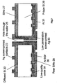
- Figure 3 shows a device according to an embodiment. It shows a semiconductor layer in the form of P-type Silicon 29 with a via in the form of a hole 25 through the wafer.
- the front side has a diffused region 20, covered by a passivation layer 27 of SiNx, with contacts 23, also called emitter contacts, extending through this passivation layer. Not shown are how the contacts would be coupled together to the conductive path in the via to pass the front side current to the bus bars, also called emitter bus bars, at the rear side.
- an i-perc type structure is shown, in the form of a dielectric stack formed by an oxide layer 39, covered by a SiNx layer 28. This can be implemented using the examples shown in WO2006 097303 .
- AI-BSF 36 are shown reached by AI (31) extending through holes in the dielectric stack to couple the base contacts together.
- the dielectric stack extends into the via.
- the deposited oxide extends all the way through the via, and the SiNx extends at least part way through.
- the conductive path in the via is printed directly on the oxide or the SiNx, partly from the front side and partly from the rear side. It can also be printed in one step, either from the rear side or from the front side, using specific vacuum conditions to suck the paste in the via if needed.
- this embodiment of a photovoltaic device has a semiconductor substrate, having at least a radiation receiving front surface and a rear surface, said substrate comprising a first region of one conductivity type (29), (can be a base region) and a second region with the opposite conductivity type (20) (can be an emitter region) adjacent to the front surface, and covered by an antireflection layer (27).
- the rear surface is covered by a dielectric layer(39) such as a deposited oxide layer or dielectric stack comprising oxide layer and silicon nitride layer (28), said dielectric layer or dielectric stack covering also an inside surface of the via.
- the front surface has current collecting conductive contacts (23) to the said second region(20) and a conductive layer extending into the via (25), the rear surface having current collecting conductive contacts (31) extending through the said dielectric to the said first region(29) and a rear conductive termination electrode (bus bar) (33).
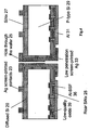
- Fig 4 shows the embodiment of the invention in which corresponding reference numerals are used to those of figure 3 .
- the SiNx extends in the via all the way through the wafer to the front surface. In some cases it can be deposited all the way through and yet in later manufacturing steps the SiNx can be removed locally in the via near the front surface, to leave an SiNx layer as shown in Fig 3 . This local removal can for example take place by the application of the front metal pastes and the subsequent firing step.
- the Example shown in Fig 4 also shows the rear busbar in the form of the screen printed Ag 33 being printed before the front grid is printed (in the form of Ag screen printed contacts 23).
- Figure 5 shows a similar embodiment, with similar reference numerals, but with the SiNx layer on the rear side not extending into the via.
- FIG. 6 shows method steps according to an embodiment.
- via's are cut through the wafer by means of laser or any other silicon machining or etching method.
- an N+ diffusion layer is created on the front side of the P-type Si.
- the SiNx and other front side layers if any, are then formed. In principle this step could be carried out before the vias are cut. Either way it is preferable to avoid creating the diffusion layer near the vias so that it does not extend deeper adjacent the vias.
- the dielectric layer is formed all over the back surface without aligning or patterning, so it will extend into the vias. Other layers of the dielectric stack are formed on the dielectric layer, optionally extending into the via at step 59.
- the dielectric stack is locally opened.
- emitter metallization is formed.
- the emitter busbars are formed on the rear to connect multiple vias together and to collect all the front side current, as shown as step 68.
- the emitter contact grid is formed on the front. They are connected to each other through the via.
- the emitter electrode extending into the via, and over the dielectric layer is isolated from the base of the semiconductor by the dielectric layer. Forming such conductive paths in the vias can be implemented in various different ways as would be known to those skilled in the art.
- metal is deposited to fill the back-contact holes through the dielectric layer to reach the semiconductor. These accesses to the base of the semiconductor are connected together.
- the device is fired, to do thermal processing of the back and front contacts.
- the embodiments described show a semiconductor layer in the form of a silicon substrate, but the invention is not limited thereto. Other suitable substrates can be used as well.
- the dielectric layer can be implemented by a wide bandgap semiconductor layer acting as a dielectric. There can be many vias closely spaced in a regular pattern so as to minimise losses and minimise the amount of shading by the metal on the front side. A typical spacing might be 2mm, though other values can be used.
- the front side contacts can be arranged in star patterns radiating away from each via, or other patterns can be used following known practice.
- the semiconductor layer has a diffusion region, formed by diffusion from the front surface and formed so that the diffusion region does not extend deeper into the semiconductor layer in the vicinity of the via.
- a passivation layer comprising hydrogenated SiN is provided in the dielectric stack on top of said dielectric layer. The passivation layer extends into the via.
- the busbar of the emitter contact formed on the rear side can be formed after the firing of the front grid and of the rear contact, using for instance a low-temperature paste.
- the emitter busbar can be printed before the front grid so that the material of the busbar is in direct contact with the dielectric isolating layer. This material provides an additional protection against penetration of the paste used for the front grid, which can be more aggressive because it needs to penetrate during firing through the SiNx deposited as ARC layer on the front.
- the rear SiN layer or SiN:H layer can have a thickness larger than 100 nm, preferably larger than 120 nm, still more preferred larger than 150 nm, larger than 180 nm or larger than 200 nm.
- both the front main surface and the rear surface are adapted to receive impinging light.
- the front main surface is that surface adapted for receiving the largest fraction of the impinging light.
- the layer of hydrogenated SiN functions as a passivating layer in that it releases hydrogen (during a subsequent high-temperature step) and induces the charges that allow for a good surface passivation of the dielectric/substrate interface.
- the dielectric layer on the rear surface may comprise depositing a low quality oxide.
- the low quality oxide may comprise low quality amorphous oxide, e.g. amorphous silicon oxide, which can reduce production costs when compared to production of high quality oxide.
- the low-quality amorphous oxide may be any of APCVD pyrolithic oxide, spin-on oxide, spray-on oxide or dip oxide.
- the dielectric layer may be a deposited dielectric layer. Deposited dielectric layers are typically of lower quality than grown dielectric layers.
- a low-quality dielectric layer e.g. amorphous oxide
- the deposition temperature may be lower than 600°C, hereby allowing processing without thermal poisoning of substrates.
- the dielectric may be deposited e.g. by PECVD at a temperature below 500 °C.
- the deposition temperature may be lower than 410 °C, which can be achieved by using for instance pyrox (having a typical deposition temperature of 404 °C).
- the dielectric or wide bandgap semiconductor layer may be deposited by low temperature PEVCD ( ⁇ 300°C).
- the deposition may be done at Room Temperature e.g. by spin-on, spray-on, dip or any other deposition from liquid, sol, solgel.
- the resulting dielectric layer or wide bandgap semiconductor layer may need further curing at higher temperatures, which can happen during further cell processing.
- any kind of silicon substrate may be used.
- silicon substrates are Czochralski Si (cz-Si) wafers, Floaf-Zone Si (fz-Si) wafers, multicrystalline Si (mc-Si) wafers and Ribbon Si waters.
- layers are polycrystalline silicon layers which can be put on glass or glass-ceramic, or monocrystalline Si layers obtained by a lift-off process
- the thickness of the dielectric layer or wide bandgap semiconductor layer or sub-stack of dielectric layers and/or wide bandgap semiconductor layers may be between 100 nm and 5000 nm, preferably between 100 nm and 4000 nm, more preferred between 100 nm and 3000 nm, still more preferred between 100 nm and 2000 nm, still more preferred between 100 nm and 1500 nm, still more preferred between 150 nm and 1200 nm, more preferably between 200 nm and 1200 nm, still more preferably between 600 nm and 1200 nm or between 800 nm and 1200 nm.
- the thickness of the dielectric layer or wide bandgap semiconductor layer or dielectric layer stack may be between 400 nm and 800 nm.
- the minimal thickness of the dielectric layer or wide bandgap semiconductor layer or dielectric layer stack depends on the material which is employed and is determined by the amount of material which is necessary to act simultaneously as a diffusion mask during emitter diffusion, while still being of use for surface passivation and contact formation. For pyrox Silicon Oxide this is typically about 300 nm, for Al 2 O 3 /TiO 2 pseudobinary alloys (PBAs) deposited by solgel this is about 150 nm. Those thickness values are only indicative and a deviation of 10%, 20% or more from the given values is possible. Also a combination, or a stack of layers, of different materials are possible and would lead to a pre-determined threshold thickness for the combined diffusion mask, surface passivation and contact formation process.
- a thicker oxide deposited in the vias is expected to create a better isolation between the emitter electrode and the base of the semiconductor layer in the via and in the busbar region on the rear.
- Deposition of such low-quality dielectric layers may be performed by low-cost deposition techniques which may be fast.
- forming back contacts may comprise forming holes in said dielectric layer or wide bandgap semiconductor layer and said passivation layer or in said dielectric layer stack possibly provided with a passivation layer, and depositing a layer of contacting material onto said passivation layer or onto said dielectric layer stack, hereby filing said holes.
- Forming holes may be performed by applying an etching paste, by mechanical scribing or by laser ablation for example.
- depositing a layer of contacting material may be performed by evaporation, sputtering or screen printing, inkjet printing, stencil printing.
- Metals can be used as contacting materials, although advantageously Aluminum can be used. Some embodiments involve using Aluminum paste, allowing the formation of local BSF (Back Surface Field) contacts.
- a metal instead of a metal, a p+ (or n+ on n-type substrates) semiconductor (like a-Si) by e.g. PECVD and then deposit a metal on top of it.
- the layer of contacting material may be discontinuous. During the step of depositing the layer of contacting material, said contacting material may be deposited essentially in said holes. Different ways of depositing such a discontinuous layer of contact material exist, and are known by a person of ordinary skill.
- the layer of contacting material may be initially discontinuous. This means that different areas can be covered with contacting material, whereby those different areas are not electrically connected to each other. These areas can be electrically connected later on in order to allow an optimal current flow through the device and/or an external load.
- the layer of contacting material may be deposited in such way that light can also enter the device from the rear side, thereby allowing the production of bifacial solar cells.
- a high temperature step may be applied to the layer of contacting material, i.e. a step at a temperature between 600 and 1000 degrees Celsius, such as for example firing of the front and rear contacts in a rapid thermal process (tens of seconds).
- a temperature between 600 and 1000 degrees Celsius such as for example firing of the front and rear contacts in a rapid thermal process (tens of seconds).
- the method according to the present invention be used with the high temperature step, but the dielectric layer or wide bandgap semiconductor layer or dielectric layer stack can be resistant to such a high temperature step, which is typical in all industrial solar cells.
- the surface passivation of the dielectric/silicori interface can be improved.
- This high temperature step may e.g.
- the firing step can be "co-firing" when the front and rear side contact are created at the same time.
- the rear side can be fired above 800 degrees Celsius, and subsequently the front contact can be fired around 750 degrees Celsius (and possibly followed by a forming gas anneal -FGA-)
- the numbers in the last paragraph are indicative and certain variations are possible (e.g. of about 25%).
- forming back contacts may be performed by applying a continuous layer of contacting material, e.g. metal, and applying local firing of the layer of contacting material, i.e. local heating e.g. by means of a laser.
- the continuous layer of contacting material can also serve as a back mirror.
- forming back contacts may be performed by applying a patterned metal layer at the passivated rear surface of the photovoltaic device, for instance solar cell, and applying a general heating : step.
- Some embodiments of methods may further comprise a step of diffusion and emitter removal on the surface to be passivated (i.e. rear surface) before depositing said dielectric layer or wide bandgap semiconductor layer or said dielectric layer stack.
- a step of diffusion and emitter removal on the surface to be passivated i.e. rear surface
- these layers may be applied before the formation of the emitter takes place. In this case, no dopants will enter into the substrate at the rear surface of the device, and thus it is advantageous that according to some embodiments of the present invention emitter removal on the surface to be passivated may be avoided.
- a step of diffusion may be applied after the step of depositing a dielectric layer or wide bandgap semiconductor layer and before the step of depositing a passivation layer.
- the dielectric layer or wide bandgap semiconductor layer may be used as a diffusion mask.
- the dielectric layer or wide bandgap semiconductor layer can be used simultaneously as a diffusion mask and for the purpose of surface passivation, thereby simplifying the cell process sequence.
- the dielectric layer or a wide bandgap semiconductor layer can be used as a diffusion mask, whether it is patterned or not. Normally it will not be patterned, and it is just a mask on the full rear surface. It may, however, be patterned e.g. for interdigitated or back contacted solar cells. Later on, the dielectric layer or wide bandgap semiconductor layer, whether patterned or not, may be locally removed, ablated, etched or patterned in order to create openings for local contacts to the substrate surface.
- a further step can be comprised of diffusion with another mask to be etched off, or maskless diffusion with subsequent rear side parasitic emitter removal before depositing the dielectric layer or wide bandgap semiconductor layer.
- said front surface may have undergone a typical solar cell front surface processing.
- a typical solar cell front surface process may comprise texturing of the front surface, diffusion of phosphorus atoms at the front side, etching of the phosphorus glass and the deposition of a silicon nitride layer on the front side.
- the method steps as recited hereinabove for the rear surface may also be applied to the front main surface of the solar cell.
- the substrate e.g. silicon substrate
- the substrate may be an ultra-thin substrate, which is typically thinner than 250. micron, preferably thinner than 200 micron, or more preferably thinner than 150 micron. Reducing the thickness of the substrate allows a more efficient use of prime material, hence a lower cost.
- ultra-thin substrates may bow under or after certain treatments. Some embodiments of the present invention can improve the resistance against bowing of such ultra-thin substrates, therefore reducing at least some of the difficulties of the use of ultra-thin substrates for photovoltaic device, for instance solar cell, fabrication.
- a thick SiN layer is deposited on a rear surface of a silicon substrate.
- the SiN layer has a thickness larger than 100 nm, preferably a thickness of at least 180 nm.
- the cell efficiencies for dielectric layers thicker than 100 nm have been found to be better than prior art cell efficiencies with lower dielectric thicknesses.
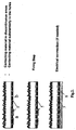
- Fig.1 shows stages in a manufacturing process according to an embodiment, without showing the via.
- dielectric e.g. oxide
- substrate surface 4 e.g. silicon surface.
- SiNx:H 3 optimized for hydrogen release is deposited.
- the substrate surface passivation is improved by means of hydrogenation.
- the dielectric layer stack 1, 3 thus formed is then opened up by forming holes 6 in the stack, to form local contact areas.
- a layer of contacting material 5 is applied onto said dielectric layer stack 1, 3, hereby filling the holes. This may be done by screen printing, for example by simultaneously or consecutively front and rear side screen printing.
- a high temperature step such as co-firing is then applied in order to make contact with the substrate 2.
- the contacting material 5 may be applied as a continuous layer, or as a discontinuous layer as in Fig. 2 . This means that different areas can be covered with contacting material 5, whereby those different areas are not electrically connected to each other. These areas can be electrically connected later on by electrical connection means 8 in order to allow an optimal current flow through the device and/or an external load.
- a rear side passivation layer has thus been developed that (a) retains or improves its surface passivation qualities during the firing step, that (b) cannot be fired through by commercial Aluminum screen printed paste, while there exists a least-damage, fast technique to locally remove such layer prior to metallisation, and that (c) does not interact with the capping metal layer during the firing process or when local contacts are otherwise formed through it.
- a generic low quality amorphous oxide was deposited (e.g. SiO 2 , SiOx, SOG, TiO 2 , Al 2 O 3 ... or their pseudo-alloys, SiONx,) on the solar cell's rear side silicon surface (e.g. by APCVD, or spin coating).
- the surface passivation properties of the dielectric layer were improved by depositing an optimized hydrogenated dielectric layer (namely: SiNx:H).
- SiNx:H optimized hydrogenated dielectric layer
- this invention enables for an easy way to create Local Back Surface Field (LBSF) contacts by selective alloying, during the firing process itself.
- the alloying process partially recovers any surface damage that may have incurred during the opening of the layer, thereby further simplifying the process.
- part of the Si surface and subsurface forms an alloy with the metal.
- the surface termination is therefore not crucial, as it would be e.g. when depositing another semiconductor, or a dielectric. A back surface field is formed and the effect of residual subsurface damage will be reduced, to a certain extent.
- silicon oxide 1 was deposited by atmospheric pressure chemical vapor deposition (APCVD) onto a silicon substrate 2.
- APCVD oxide has poor passivation properties and finds its application in microelectronics as an inexpensive and convenient diffusion mask, or dopant source. In fact, it can be deposited at about 400 °C, which means that even low quality silicon material can withstand the deposition process without risk of thermal poisoning.
- Thermal annealing can, to some extent, improve the surface passivation quality of APCVD oxide. However, prolonged treatments lead to a degradation of the sample.
- Hydrogenated silicon nitride (SiNx:H) 3 is used to stably improve the quality of the oxide/silicon interface 4. It is known that silicon nitride can lead to excellent surface and bulk passivation properties on silicon, reason for which it is widely used in solar cell technology. However, its application for rear side passivation of an industrial solar cell is not straightforward. There exists an interaction between silicon nitride and metal capping layer (i.e. the rear surface contact of the solar cell), that leads to decreased surface passivation and cell efficiency (it is believed that this interaction is more than a "shunt" effect as described e.g.
- the silicon nitride is used as a hydrogen source for the low quality oxide underneath, thereby significantly improving its surface passivation properties.
- the oxide layer in one experiment was 800 nm thick, excluding any field-induced passivation effect from the overlying silicon nitride, which is in the prior art believed to be the reason for the good passivation quality.
- a further advantage of the technique is that since it can be applied to low quality oxides, it can be applied directly on diffusion mask oxides too, greatly simplifying the solar cell process.
- Dielectric layer stacks with a dielectric layer with thickness between 100 nm and 1500 nm have been deposited.
- the open circuit voltage has been measured as a function of the low quality dielectric thickness.
- Dielectric thicknesses between 100 nm and 800 nm provide improved open circuit voltages with respect to the open circuit voltage of a cell obtained by a standard prior art process of full coverage aluminium BSF.
- stacks than the above-mentioned silicon (substrate)/low quality oxide (dielectric layer)/silicon nitride (passivation layer) stack can for example be, however , without being part of the invention,
- a typical process sequence for surface passivation including inside the vias can comprise the steps of
- MWT cell Another problem with the known MWT cell arises from metallization in the vias and on the rear side being printed directly on the "non-covered" n+ layer, rather than on top of the silicon nitride antireflection coating layer as happens on the front side. It is very difficult to find the right contact firing process so that the front metallization has low contact resistance and the metallization in the vias does not create shunts. If the firing temperature is too high, metal spiking creates significant shunts. This again reduces performance.
- the n+layer on the rear is in direct contact with the Al-BSF layer which results in shunting.
- Laser junction isolation is applied to separate n+ and p+ regions. Any imperfection in this step of junction isolation contributes to shunts.
- there is no n+ layer on the rear surface and both polarity electrodes are printed on dielectric so there is no need for any additional isolation.
- the constraints of alignment of the two polarity contacts are also relaxed since the metal printing by itself defines the contact isolation, and not an additional laser step, which has to be aligned to the gap between the 2 contacts in the MWT structure.
- a possible difficulty or source of weakness occurs where the front-contact metal paste is very close to the base region of the substrate and separated from it by the oxide layer deposited in the vias (particularly at the intersection of the via and the front surface).
- the dielectric being a lot thinner than on the rear surface.
- the front side Ag paste did get through the SiNx layer during firing, and thus damage the Si. So there were grounds for predicting that it might get through the SiNx layer + a rather thin (but thickness extremely difficult to quantify) oxide layer at the front side edge of the via.
- the iPERC stack optimized for base passivation proved to provide an unexpectedly efficient protection layer against the penetration of the Ag paste.
- the new structure also proves to be better in terms of avoiding a loss in fill factor (FF) which occurs when the diffusion extends along the vias. Also, it is notable that the thick dielectric needed to protect the busbar region if you do not diffuse the vias, can also be used as the thick dielectric needed for the i-PERC process for the back side.
- FF loss in fill factor
Landscapes
- Photovoltaic Devices (AREA)
- Life Sciences & Earth Sciences (AREA)
- Engineering & Computer Science (AREA)
- Sustainable Development (AREA)
- Sustainable Energy (AREA)
Abstract
Description
- The present invention is related to photovoltaic devices such as solar cells. More particularly it relates to metal wrap through solar cells improved by specific passivation scheme, and to a cost effective method of manufacturing the same.
- Most solar cells described in the prior art can be subdivided into several categories according to their general structure.
- One of these categories is the group of the so called back-contacted solar cells, meaning that both ohmic contacts to the two oppositely doped regions of the solar cells are placed on the back or non-illuminated surface of the solar cell. This concept avoids or reduces shadowing losses caused by the front metal contact grid on standard solar cells.
- The most straightforward way to fabricate back contact solar cells is to place the carrier collecting junction between semiconductor regions of opposite doping close to the back surface of the cell ("back-junction" cell). The document "1127.5-Percent Silicon Concentrator Solar Cells" (R.A. Sinton, Y. Kwark, J.Y. Gan, R.M. Swanson, IEEE Electron Device Letters, Vol. ED-7. No. 10, October 1986) describes such a device.
- Since the majority of photons are always absorbed close to the front surface of the cell, the generated carriers in these regions have to diffuse through the entire base region of the cell towards the carrier collecting junction close to the back surface. For this concept, high quality material with minority carrier diffusion lengths longer than the cell thickness is needed, which makes this solution not applicable for most solar grade materials which generally have short diffusion lengths. Additionally, a perfect front surface passivation is required for cells having the carrier collecting junction close to the back surface.
- The largest group of solar cells has the carrier collecting junction close to its front surface. The current from these solar cells is collected by a metal contact to the doped region on the front surface and by a second contact to the oppositely doped region on the back surface. Although this front grid structure can be optimized relatively easily in order to get high collection efficiencies, the trade off between resistance losses and shading losses necessitates a coverage of the front surface by 6-12% of the total area.
- Another group of solar cells combines the two approaches. Such solar cells have both external contacts to the oppositely doped regions on the back surface and the collecting junction close to the front surface. The collected current from the front surface is lead through openings, which extend through the entire wafer, to the back surface. Using this structure, shading losses normally arising from the front metallization grid are greatly reduced.
- The document
WO 1998/054763 (EP 0 985 233 B1 ) describes such a structure hereafter called Metal Wrap Through (MWT). - Despite their decreased shadowed area those MWT solar cells are still generally efficiency limited due to excessive shunt like recombination happening in the via and under the rear emitter bus bars (as disclosed e.g. in documents: "Processing and comprehensive characterisation of screen-printed MC-Si Metal Wrap Through (MWT) Solar cells", Clement et al.., Proceedings of the 22nd European Photovoltaic Solar Energy Conference, Milan, Italy (2007), p1400-1402; "Lifetime studies on laser drilled vias for application in Emitter-Wrap-Through-Solar Cells", Mingirulli et al., Proceedings of the 22nd European Photovoltaic Solar Energy Conference, Milan, Italy (2007), p1415-1418).
- US patent application
US2007186971 and US patentUS3903427 disclose "Metal Wrap Through" solar cells wherein the dielectric layer covering the inside surface of the via to insulate the conductive path from the semiconductor layer is disposed on the rear surface of the semiconductor layer and the back contact extends through the dielectric layer to the semiconductor. - German patent application
DE19650111 , European patent applicationEP528311 PCT application WO8905521
US 4,610,077 discloses a photovoltaic device according to the preamble of claim 1.
InWO2006/097303 a method is disclosed for the production of a photovoltaic device, comprising the steps of providing a substrate having a front main surface and a rear surface; depositing a dielectric layer on the rear surface, depositing a passivation layer comprising hydrogenated SiN on top of the dielectric layer and forming back contacts through the dielectric layer and the passivation layer. - It is an aim of this invention to provide photovoltaic cells and a method for producing a photovoltaic cell, which alleviates or avoids some problems of the prior art.
- In a first aspect of the present invention, there is provided a photovoltaic device as for instance a solar cell, the photovoltaic device having a semiconductor layer having a front surface for receiving impinging light, e.g. sunlight, and a rear surface opposite to the front surface, a front contact, also called emitter contact, for collecting current on the front surface, a rear bus bar, also called emitter busbar, on the rear of the device, e.g. on a rear surface for extracting front side current, a via through the semiconductor layer, the via having a conductive path for coupling the front contact to the rear bus bar, a dielectric layer on a rear surface of the substrate i.e. on the rear surface of the semiconductor layer, a back contact for the rear surface of the semiconductor layer, extending through the dielectric layer to the semiconductor layer, wherein the dielectric layer also covers an inside surface of the via to insulate the conductive path from the semiconductor layer.
- Compared to existing designs having vias, by providing the same dielectric inside the via, rather than having some other specific insulation in the via, it is not necessary to have steps for aligning and masking, to keep the dielectric away from the via. Hence manufacturing can be cheaper or quicker. Furthermore, the dielectric in the via helps reduce the need to have a junction region near the via and on the back surface, so there is less damage from drilling the via present in or next to the junction region. This helps reduce unwanted recombination currents, thus improving efficiency. Thus the dielectric can serve multiple purposes, such as surface and bulk passivation, protection against thermal damage caused by firing, back surface reflecting to improve efficiency, and insulating the metal from the semiconductor in the via.
- Rear-contacted solar cells usually experience more bowing than conventional solar cells since there is no bus bar on the front to compensate for the high stress induced by Al paste on the rear. Here, thanks to the dielectric stack, the solar cells produced show much less of the detrimental bowing problem.
- Another aspect of the invention provides a method of manufacturing a photovoltaic device having a semiconductor layer having a front surface for receiving impinging light, e.g. sunlight, and a rear surface opposite to the front surface, the method having the steps of forming a via through the semiconductor layer,
forming a dielectric layer on a rear surface of the substrate, i.e. on the rear surface of the semiconductor layer, such that the dielectric layer also covers an inside surface of the via,
forming a conductive path through the via, for collecting current from the front surface, and insulated from the semiconductor layer by the dielectric layer, forming a rear bus bar on the rear of the device e.g. on the rear surface thereof to couple the conductive path through the via, and a back contact for the rear surface of the semiconductor layer, extending through the dielectric layer to the semiconductor layer. - Particular and preferred aspects of the invention are set out in the accompanying independent and dependent claims. Embodiments of any aspect of the invention can have any additional features, and some such additional features are set out in dependent claims, and some are set out in the examples in the detailed description. Features from the dependent claims may be combined with features of the independent claims and with features of other dependent claims as appropriate and not merely as explicitly set out in the claims.
-
-
Fig.1 . shows an example of stages in a photovoltaic device, as e.g. a solar cell, fabrication process according to an embodiment. -
Fig.2 . shows an illustration of stages in other fabrication processes according to other embodiments. -
Fig 3 shows a cross section view of a photovoltaic device according to an embodiment. -
Fig 4 shows a similar cross section view according to the embodiment of the invention. -
Fig 5 shows a cross section view of a photovoltaic device according to another embodiment. -
Fig 6 shows steps in a method of manufacturing according to another embodiment. - The embodiment of
Fig. 4 is the only embodiment of the invention. - How the present invention can be put into effect will be described with reference to certain drawings. The drawings described are only schematic and are non-limiting. In the drawings, the size of some of the elements may be exaggerated and not drawn on scale for illustrative purposes.
- Furthermore, the terms first, second, third and the like in the description and in the claims, are used for distinguishing between similar elements and not necessarily for describing a sequential or chronological order. It is to be understood that the terms so used are interchangeable under appropriate circumstances and that the embodiments of the invention described herein are capable of operation in other sequences than described or illustrated herein.
- Moreover, the terms top, bottom, over, under and the like in the description and the claims are used for descriptive purposes and not necessarily for describing relative positions. It is to be understood that the terms so used are interchangeable under appropriate circumstances and that the embodiments of the invention described herein are capable of operation in other orientations than described or illustrated herein.
- The embodiments described show a new and improved structure which has some of the features of the known MWT structure mentioned above, and of the so called i-perc structure described in the document
WO 2006/097303 A1 . The new structure (called i-perc-BC) benefits from the stable passivating stack of the i-perc deposited not only on the rear side but also in the via. An important difference of at least some embodiments compared to the known MWT structure is the absence of diffusion in via and on the rear side. A consequence of this is the reduction or avoidance of defects generated during the via formation being present in the emitter and/or in the depletion region. Such defects cause recombinations which reduces performance. In addition to its beneficial passivating properties, the stack will also serve as a barrier between the metal paste electrically connected to the emitter and covering via and a portion of the rear surface and the underneath bare base region. - In the i-perc structure the stack extends over the whole base region and is only locally opened for contact formation which provides excellent passivation of the surface on the base side. Similarly, in the new structure, the stack provides passivation in the regions covered by base electrode and also in base like regions located in between the emitter and base electrode on the rear side.
- From a processing point of view the new structure presents also an advantage compared to the initial MWT structure to be found in a simplification of the solar processing due to absence of need for junction isolation both on the rear and on the front side as a consequence of the absence of emitter regions on the rear side.
-
Figure 3 shows a device according to an embodiment. It shows a semiconductor layer in the form of P-type Silicon 29 with a via in the form of ahole 25 through the wafer. The front side has a diffused region 20, covered by apassivation layer 27 of SiNx, withcontacts 23, also called emitter contacts, extending through this passivation layer. Not shown are how the contacts would be coupled together to the conductive path in the via to pass the front side current to the bus bars, also called emitter bus bars, at the rear side. On the rear side, an i-perc type structure is shown, in the form of a dielectric stack formed by anoxide layer 39, covered by aSiNx layer 28. This can be implemented using the examples shown inWO2006 097303 . Back contacts, also called rear contacts or base contacts, AI-BSF 36 are shown reached by AI (31) extending through holes in the dielectric stack to couple the base contacts together. The dielectric stack extends into the via. The deposited oxide extends all the way through the via, and the SiNx extends at least part way through. The conductive path in the via is printed directly on the oxide or the SiNx, partly from the front side and partly from the rear side. It can also be printed in one step, either from the rear side or from the front side, using specific vacuum conditions to suck the paste in the via if needed. - In other words, this embodiment of a photovoltaic device has a semiconductor substrate, having at least a radiation receiving front surface and a rear surface, said substrate comprising a first region of one conductivity type (29), (can be a base region) and a second region with the opposite conductivity type (20) (can be an emitter region) adjacent to the front surface, and covered by an antireflection layer (27). The rear surface is covered by a dielectric layer(39) such as a deposited oxide layer or dielectric stack comprising oxide layer and silicon nitride layer (28), said dielectric layer or dielectric stack covering also an inside surface of the via. The front surface has current collecting conductive contacts (23) to the said second region(20) and a conductive layer extending into the via (25), the rear surface having current collecting conductive contacts (31) extending through the said dielectric to the said first region(29) and a rear conductive termination electrode (bus bar) (33). This extends into the via and together with the front
conductive layer 23 forms a conductive path for photogenerated current from the front surface to a termination electrode (33) on the rear. By having the dielectric all over, no aligning and masking is needed, and the same dielectric serves to insulate, provide thermal protection for the semiconductor, and helps in surface and bulk passivation. It also avoids the need for a junction region near the via, so reducing damage to the junction region near the via from a manufacturing process of the via and hence reducing unwanted recombination currents. -
Fig 4 shows the embodiment of the invention in which corresponding reference numerals are used to those offigure 3 . Compared tofig 3 , the SiNx extends in the via all the way through the wafer to the front surface. In some cases it can be deposited all the way through and yet in later manufacturing steps the SiNx can be removed locally in the via near the front surface, to leave an SiNx layer as shown inFig 3 . This local removal can for example take place by the application of the front metal pastes and the subsequent firing step. The Example shown inFig 4 also shows the rear busbar in the form of the screen printedAg 33 being printed before the front grid is printed (in the form of Ag screen printed contacts 23). -
Figure 5 shows a similar embodiment, with similar reference numerals, but with the SiNx layer on the rear side not extending into the via. -
Figure 6 shows method steps according to an embodiment. Atstep 54 via's are cut through the wafer by means of laser or any other silicon machining or etching method. At step 52, an N+ diffusion layer is created on the front side of the P-type Si. The SiNx and other front side layers if any, are then formed. In principle this step could be carried out before the vias are cut. Either way it is preferable to avoid creating the diffusion layer near the vias so that it does not extend deeper adjacent the vias. Atstep 57, the dielectric layer is formed all over the back surface without aligning or patterning, so it will extend into the vias. Other layers of the dielectric stack are formed on the dielectric layer, optionally extending into the via atstep 59. Atstep 64, the dielectric stack is locally opened. Atsteps 62 and 68, emitter metallization is formed. The emitter busbars are formed on the rear to connect multiple vias together and to collect all the front side current, as shown as step 68. Then the emitter contact grid is formed on the front. They are connected to each other through the via. The emitter electrode extending into the via, and over the dielectric layer is isolated from the base of the semiconductor by the dielectric layer. Forming such conductive paths in the vias can be implemented in various different ways as would be known to those skilled in the art. Atstep 66, metal is deposited to fill the back-contact holes through the dielectric layer to reach the semiconductor. These accesses to the base of the semiconductor are connected together. Atstep 72, the device is fired, to do thermal processing of the back and front contacts. - The embodiments described show a semiconductor layer in the form of a silicon substrate, but the invention is not limited thereto. Other suitable substrates can be used as well. The dielectric layer can be implemented by a wide bandgap semiconductor layer acting as a dielectric. There can be many vias closely spaced in a regular pattern so as to minimise losses and minimise the amount of shading by the metal on the front side. A typical spacing might be 2mm, though other values can be used. The front side contacts can be arranged in star patterns radiating away from each via, or other patterns can be used following known practice. The semiconductor layer has a diffusion region, formed by diffusion from the front surface and formed so that the diffusion region does not extend deeper into the semiconductor layer in the vicinity of the via. A passivation layer comprising hydrogenated SiN is provided in the dielectric stack on top of said dielectric layer. The passivation layer extends into the via.
- The busbar of the emitter contact formed on the rear side can be formed after the firing of the front grid and of the rear contact, using for instance a low-temperature paste.
- The emitter busbar can be printed before the front grid so that the material of the busbar is in direct contact with the dielectric isolating layer. This material provides an additional protection against penetration of the paste used for the front grid, which can be more aggressive because it needs to penetrate during firing through the SiNx deposited as ARC layer on the front. The rear SiN layer or SiN:H layer can have a thickness larger than 100 nm, preferably larger than 120 nm, still more preferred larger than 150 nm, larger than 180 nm or larger than 200 nm.
- In case of bifacial solar cells, both the front main surface and the rear surface are adapted to receive impinging light. In that case, the front main surface is that surface adapted for receiving the largest fraction of the impinging light.
- The layer of hydrogenated SiN functions as a passivating layer in that it releases hydrogen (during a subsequent high-temperature step) and induces the charges that allow for a good surface passivation of the dielectric/substrate interface.
- The dielectric layer on the rear surface may comprise depositing a low quality oxide. The low quality oxide may comprise low quality amorphous oxide, e.g. amorphous silicon oxide, which can reduce production costs when compared to production of high quality oxide. The low-quality amorphous oxide may be any of APCVD pyrolithic oxide, spin-on oxide, spray-on oxide or dip oxide. In embodiments of the present invention, the dielectric layer may be a deposited dielectric layer. Deposited dielectric layers are typically of lower quality than grown dielectric layers.
- A low-quality dielectric layer, e.g. amorphous oxide, can for instance be a Spin-on oxide or APCVD (Atmospheric pressure chemical vapour deposition) pyrolithic oxide (pyrox), spin-on, spray-on or dip oxide. It can be for instance a silicon oxide, TiO2 (e.g. deposited by solgel), or Al2O3/TiO2 pseudobinary alloys (PBAs)..
- Depositing the dielectric layer or wide bandgap semiconductor layer at certain temperatures may bring certain advantageous effects, some of which are described below. In embodiments of the present invention, the deposition temperature may be lower than 600°C, hereby allowing processing without thermal poisoning of substrates. In embodiments of the present invention, the dielectric may be deposited e.g. by PECVD at a temperature below 500 °C. In embodiments of the present invention, the deposition temperature may be lower than 410 °C, which can be achieved by using for instance pyrox (having a typical deposition temperature of 404 °C). In embodiments of the present invention the dielectric or wide bandgap semiconductor layer may be deposited by low temperature PEVCD (< 300°C). In other embodiments of the present invention, the deposition may be done at Room Temperature e.g. by spin-on, spray-on, dip or any other deposition from liquid, sol, solgel. The resulting dielectric layer or wide bandgap semiconductor layer may need further curing at higher temperatures, which can happen during further cell processing.
- In some of the embodiments if a silicon substrate is used, any kind of silicon substrate may be used. Some examples of silicon substrates are Czochralski Si (cz-Si) wafers, Floaf-Zone Si (fz-Si) wafers, multicrystalline Si (mc-Si) wafers and Ribbon Si waters. Some examples of layers are polycrystalline silicon layers which can be put on glass or glass-ceramic, or monocrystalline Si layers obtained by a lift-off process
- In some of the embodiments, the thickness of the dielectric layer or wide bandgap semiconductor layer or sub-stack of dielectric layers and/or wide bandgap semiconductor layers may be between 100 nm and 5000 nm, preferably between 100 nm and 4000 nm, more preferred between 100 nm and 3000 nm, still more preferred between 100 nm and 2000 nm, still more preferred between 100 nm and 1500 nm, still more preferred between 150 nm and 1200 nm, more preferably between 200 nm and 1200 nm, still more preferably between 600 nm and 1200 nm or between 800 nm and 1200 nm. Alternatively, the thickness of the dielectric layer or wide bandgap semiconductor layer or dielectric layer stack may be between 400 nm and 800 nm. In some embodiments of the present invention, the minimal thickness of the dielectric layer or wide bandgap semiconductor layer or dielectric layer stack depends on the material which is employed and is determined by the amount of material which is necessary to act simultaneously as a diffusion mask during emitter diffusion, while still being of use for surface passivation and contact formation. For pyrox Silicon Oxide this is typically about 300 nm, for Al2O3/TiO2 pseudobinary alloys (PBAs) deposited by solgel this is about 150 nm. Those thickness values are only indicative and a deviation of 10%, 20% or more from the given values is possible. Also a combination, or a stack of layers, of different materials are possible and would lead to a pre-determined threshold thickness for the combined diffusion mask, surface passivation and contact formation process.
- It is one of the functions of the dielectric layers or wide bandgap semiconductor layers applied at the rear surface of a photovoltaic device, for instance a solar cell, in accordance with the present invention, to increase the distance between the back contact material and the substrate surface. It has been found, surprisingly, that, for a distance between 100 nm and 5000 nm, the larger the distance between the contacting layer at the rear surface of the photovoltaic device, for instance solar cell, and the rear surface of the substrate, the better the achieved passivation results, even with low quality dielectric materials or wide bandgap semiconductor layers being applied. It is an advantage of some embodiments of the present invention that sufficient passivation results may be achieved while using low-quality dielectrics. In addition, a thicker oxide deposited in the vias is expected to create a better isolation between the emitter electrode and the base of the semiconductor layer in the via and in the busbar region on the rear. Deposition of such low-quality dielectric layers may be performed by low-cost deposition techniques which may be fast.
- In some embodiments, forming back contacts may comprise forming holes in said dielectric layer or wide bandgap semiconductor layer and said passivation layer or in said dielectric layer stack possibly provided with a passivation layer, and depositing a layer of contacting material onto said passivation layer or onto said dielectric layer stack, hereby filing said holes.
- Forming holes may be performed by applying an etching paste, by mechanical scribing or by laser ablation for example.
- In some embodiments, depositing a layer of contacting material may be performed by evaporation, sputtering or screen printing, inkjet printing, stencil printing. Metals can be used as contacting materials, although advantageously Aluminum can be used. Some embodiments involve using Aluminum paste, allowing the formation of local BSF (Back Surface Field) contacts. Alternatively, after depositing the passivation layer and firing it, one could deposit, instead of a metal, a p+ (or n+ on n-type substrates) semiconductor (like a-Si) by e.g. PECVD and then deposit a metal on top of it.
- In some embodiments of the present invention, the layer of contacting material may be discontinuous. During the step of depositing the layer of contacting material, said contacting material may be deposited essentially in said holes. Different ways of depositing such a discontinuous layer of contact material exist, and are known by a person of ordinary skill.
- In some embodiments the layer of contacting material may be initially discontinuous. This means that different areas can be covered with contacting material, whereby those different areas are not electrically connected to each other. These areas can be electrically connected later on in order to allow an optimal current flow through the device and/or an external load.
- In some embodiments, the layer of contacting material may be deposited in such way that light can also enter the device from the rear side, thereby allowing the production of bifacial solar cells.
- In some embodiments, a high temperature step may be applied to the layer of contacting material, i.e. a step at a temperature between 600 and 1000 degrees Celsius, such as for example firing of the front and rear contacts in a rapid thermal process (tens of seconds). In general it is not essential that the method according to the present invention be used with the high temperature step, but the dielectric layer or wide bandgap semiconductor layer or dielectric layer stack can be resistant to such a high temperature step, which is typical in all industrial solar cells. In addition, during the high temperature step, for instance in a particular embodiment when using a SiNx:H/dielectric stack, the surface passivation of the dielectric/silicori interface can be improved. This high temperature step may e.g. be a contact firing step which may be performed at a temperature higher than 730 degrees Celsius and below 960 degrees Celsius, for maximum about a few tens of seconds. The firing step can be "co-firing" when the front and rear side contact are created at the same time. When this is decoupled, the rear side can be fired above 800 degrees Celsius, and subsequently the front contact can be fired around 750 degrees Celsius (and possibly followed by a forming gas anneal -FGA-) The numbers in the last paragraph are indicative and certain variations are possible (e.g. of about 25%).
- In some embodiments, forming back contacts may be performed by applying a continuous layer of contacting material, e.g. metal, and applying local firing of the layer of contacting material, i.e. local heating e.g. by means of a laser. In this case, the continuous layer of contacting material can also serve as a back mirror.
- In other embodiments, forming back contacts may be performed by applying a patterned metal layer at the passivated rear surface of the photovoltaic device, for instance solar cell, and applying a general heating : step.
- Some embodiments of methods may further comprise a step of diffusion and emitter removal on the surface to be passivated (i.e. rear surface) before depositing said dielectric layer or wide bandgap semiconductor layer or said dielectric layer stack. However, if the dielectric layer or wide bandgap semiconductor layer or said dielectric layer stack is suitable for being used as a diffusion mask, these layers may be applied before the formation of the emitter takes place. In this case, no dopants will enter into the substrate at the rear surface of the device, and thus it is advantageous that according to some embodiments of the present invention emitter removal on the surface to be passivated may be avoided.
- In a method according to embodiments, for instance according to the first embodiment of the first aspect, a step of diffusion may be applied after the step of depositing a dielectric layer or wide bandgap semiconductor layer and before the step of depositing a passivation layer.
- In the same embodiment, the dielectric layer or wide bandgap semiconductor layer may be used as a diffusion mask. In advantageous embodiments, the dielectric layer or wide bandgap semiconductor layer can be used simultaneously as a diffusion mask and for the purpose of surface passivation, thereby simplifying the cell process sequence. The dielectric layer or a wide bandgap semiconductor layer can be used as a diffusion mask, whether it is patterned or not. Normally it will not be patterned, and it is just a mask on the full rear surface. It may, however, be patterned e.g. for interdigitated or back contacted solar cells. Later on, the dielectric layer or wide bandgap semiconductor layer, whether patterned or not, may be locally removed, ablated, etched or patterned in order to create openings for local contacts to the substrate surface.
- In some embodiments, when it is not possible to use the passivation layer as a diffusion mask, a further step can be comprised of diffusion with another mask to be etched off, or maskless diffusion with subsequent rear side parasitic emitter removal before depositing the dielectric layer or wide bandgap semiconductor layer.
- In some embodiments, said front surface may have undergone a typical solar cell front surface processing. A typical solar cell front surface process may comprise texturing of the front surface, diffusion of phosphorus atoms at the front side, etching of the phosphorus glass and the deposition of a silicon nitride layer on the front side. Alternatively, the method steps as recited hereinabove for the rear surface may also be applied to the front main surface of the solar cell.
- In some embodiments, the substrate, e.g. silicon substrate, may be an ultra-thin substrate, which is typically thinner than 250. micron, preferably thinner than 200 micron, or more preferably thinner than 150 micron. Reducing the thickness of the substrate allows a more efficient use of prime material, hence a lower cost. However, ultra-thin substrates may bow under or after certain treatments. Some embodiments of the present invention can improve the resistance against bowing of such ultra-thin substrates, therefore reducing at least some of the difficulties of the use of ultra-thin substrates for photovoltaic device, for instance solar cell, fabrication.
- In one embodiment, a thick SiN layer is deposited on a rear surface of a silicon substrate. The SiN layer has a thickness larger than 100 nm, preferably a thickness of at least 180 nm. When formed into a solar cell, such structure shows increased cell efficiencies for higher dielectric thicknesses. Furthermore, the cell efficiencies for dielectric layers thicker than 100 nm have been found to be better than prior art cell efficiencies with lower dielectric thicknesses.
-
Fig.1 shows stages in a manufacturing process according to an embodiment, without showing the via. For instance more than 100 nm, 200 nm, 800 nm of dielectric 1, e.g. oxide, are deposited on thesubstrate surface 4, e.g. silicon surface. On top of the dielectric 1, a layer of SiNx:H 3 optimized for hydrogen release is deposited. The substrate surface passivation is improved by means of hydrogenation. - The dielectric layer stack 1, 3 thus formed is then opened up by forming
holes 6 in the stack, to form local contact areas. A layer of contactingmaterial 5 is applied onto said dielectric layer stack 1, 3, hereby filling the holes. This may be done by screen printing, for example by simultaneously or consecutively front and rear side screen printing. A high temperature step such as co-firing is then applied in order to make contact with the substrate 2. The contactingmaterial 5 may be applied as a continuous layer, or as a discontinuous layer as inFig. 2 . This means that different areas can be covered with contactingmaterial 5, whereby those different areas are not electrically connected to each other. These areas can be electrically connected later on by electrical connection means 8 in order to allow an optimal current flow through the device and/or an external load. - A rear side passivation layer has thus been developed that (a) retains or improves its surface passivation qualities during the firing step, that (b) cannot be fired through by commercial Aluminum screen printed paste, while there exists a least-damage, fast technique to locally remove such layer prior to metallisation, and that (c) does not interact with the capping metal layer during the firing process or when local contacts are otherwise formed through it.
- Due to its characteristics this process
- provides an efficient surface passivation, where
- it is possible to make local (BSF) contacts, and
- the process eliminates the bowing problems when using ultra-thin wafers or substrates (e.g. problems when combined with Al screen printed paste on ultra-thin wafers).
- A generic low quality amorphous oxide was deposited (e.g. SiO2, SiOx, SOG, TiO2, Al2O3... or their pseudo-alloys, SiONx,) on the solar cell's rear side silicon surface (e.g. by APCVD, or spin coating). The surface passivation properties of the dielectric layer were improved by depositing an optimized hydrogenated dielectric layer (namely: SiNx:H). Such stacks retain the passivation properties during short high temperature treatments. The passivation properties are even improved during this treatment. This feature is important as it enables the use of the contact co-firing process that takes place in most of the industrial silicon solar cells' process sequence. Moreover, given that a) it is resistant to firing; i.e. it doesn't lose its relevant characteristics, b) it cannot be fired through, but c) it is possible to create local openings or holes in it by techniques such as e.g. etching paste or laser ablation, this invention enables for an easy way to create Local Back Surface Field (LBSF) contacts by selective alloying, during the firing process itself. The alloying process partially recovers any surface damage that may have incurred during the opening of the layer, thereby further simplifying the process. During the alloying, part of the Si surface and subsurface forms an alloy with the metal. The surface termination is therefore not crucial, as it would be e.g. when depositing another semiconductor, or a dielectric. A back surface field is formed and the effect of residual subsurface damage will be reduced, to a certain extent.
- In an example, illustrated in
Fig. 1 ,silicon oxide 1 was deposited by atmospheric pressure chemical vapor deposition (APCVD) onto a silicon substrate 2. As opposed to conventional thermal oxides, or wet oxides, which are known to be excellent for surface passivation of silicon, APCVD oxide has poor passivation properties and finds its application in microelectronics as an inexpensive and convenient diffusion mask, or dopant source. In fact, it can be deposited at about 400 °C, which means that even low quality silicon material can withstand the deposition process without risk of thermal poisoning. - Thermal annealing can, to some extent, improve the surface passivation quality of APCVD oxide. However, prolonged treatments lead to a degradation of the sample.
- Moreover, it has been observed that there may be a degradation of the surface passivation qualities with air exposure.
- Hydrogenated silicon nitride (SiNx:H) 3 is used to stably improve the quality of the oxide/
silicon interface 4. It is known that silicon nitride can lead to excellent surface and bulk passivation properties on silicon, reason for which it is widely used in solar cell technology. However, its application for rear side passivation of an industrial solar cell is not straightforward. There exists an interaction between silicon nitride and metal capping layer (i.e. the rear surface contact of the solar cell), that leads to decreased surface passivation and cell efficiency (it is believed that this interaction is more than a "shunt" effect as described e.g. in Dauwe S., Mittelstädt L., Metz A., Hezel R., "Experimental evidence of parasitic shunting in silicon nitride rear surface passivated solar cells", Prog. Photovolt. Res. Appl., 10 (4), 271-278, (2002)). Also the nitride recipes which are known to be best at surface passivation cannot withstand high temperature treatments such as the one that takes place during co-firing of the contacts. On the other hand, it is known that hydrogenated silicon nitride can release hydrogen during high temperature annealing treatments. - It is believed that the silicon nitride is used as a hydrogen source for the low quality oxide underneath, thereby significantly improving its surface passivation properties. The oxide layer in one experiment was 800 nm thick, excluding any field-induced passivation effect from the overlying silicon nitride, which is in the prior art believed to be the reason for the good passivation quality.
- Right after the deposition, the surface passivation quality of the oxide is very poor. After nitride deposition on top of the oxide layer there is a limited improvement (path A) and finally when firing the samples, an excellent surface passivation is achieved. Thermal cycles, like e.g. the ones that takes place with POCl3 diffusion, lead to a limited surface passivation improvement like the one observed after nitride deposition, before firing. Nitride deposition on top of the oxide and firing, once again, lead to excellent surface passivation (path B). Firing with or without a metal layer on top leads to the same good results. It has been shown that firing alone (without the SiN layer deposition step first) is not beneficial. If firing is applied to the oxide layer alone, there is a degradation of its surface passivation properties. Nonetheless, these can be recovered by subsequent nitride deposition and firing (path C).
- A further advantage of the technique is that since it can be applied to low quality oxides, it can be applied directly on diffusion mask oxides too, greatly simplifying the solar cell process.
- Dielectric layer stacks with a dielectric layer with thickness between 100 nm and 1500 nm have been deposited. When implemented in solar cells, the open circuit voltage has been measured as a function of the low quality dielectric thickness. Dielectric thicknesses between 100 nm and 800 nm provide improved open circuit voltages with respect to the open circuit voltage of a cell obtained by a standard prior art process of full coverage aluminium BSF.
- Other stacks than the above-mentioned silicon (substrate)/low quality oxide (dielectric layer)/silicon nitride (passivation layer) stack can for example be, however, without being part of the invention,
- silicon (substrate)/dielectric or wide bandgap (>2eV, preferably >3eV) semiconductor, such as e.g. silicon carbide (SiC), aluminum nitride (AlN), gallium nitride (GaN) or boron nitride (BN) / silicon nitride
- silicon (substrate) / silicon nitride / low quality oxide
- silicon (substrate) / silicon nitride / wide bandgap (>2eV, preferably >3eV) semiconductor or dielectric
- silicon (substrate) / Al2O3 / low quality oxide
- silicon (substrate) / Al2O3 / wide bandgap (>2eV, preferably >3eV) semiconductor or dielectric
- A typical process sequence for surface passivation including inside the vias can comprise the steps of
- Chemical cleaning
- Low quality oxide deposition (100 to 1500 nm)
- Silicon nitride deposition; for instance Low Frequency (450 kHz) direct PECVD Hydrogenated SiNx deposited at 400 degrees from SiH4 and NH3 precursors
- Firing in a three-zone belt furnace, at high belt speed (e.g. more than 100 inch/min), peak set temperature of the furnace up to 960 °C
- A) deposition after diffusion
- Opening of the vias, e.g. by laser drilling
- Front side texturing
- Diffusion, e.g. Phosphorus diffusion, resulting in doped, e.g. n-type doped, regions all around the substrate, i.e. both at the front surface and the rear surface
- Glass removal, e.g. Phosphorus-glass removal,
- Etching of Si at the rear (sufficient to remove n-type doped region at rear and in the vias)
- Chemical cleaning
- Low quality oxide deposition
- Silicon nitride deposition (rear and possibly front)
- Opening of the local contacts (e.g. by etching paste, scribing or laser ablation)
- Forming the rear-contact bus bar (terminal electrode of the front contact grid connected to the front contact grid through the vias).
- Forming the front contact grid.
- Forming of base contacts (e.g. by Metal deposition for local contacts on back surface (e.g. by evaporation, sputtering, screen printing)).
- Firing in a commercial belt furnace
- B) Before diffusion
- Opening of the vias, e.g. by laser drilling
- Chemical cleaning
- Low quality oxide deposition on the back and in the vias
- Diffusion (will only take place at the front surface to form the emitter, as at the rear surface low-quality oxide has been deposited and functions as a mask for the diffusion)
- Silicon nitride deposition (rear and possibly front side)
- Opening of the local contacts (e.g. by etching paste, scribing or laser ablation)
- Forming the rear-contact bus bar (terminal electrode of the front contact grid connected to the front contact grid through the vias).
- Forming the front contact grid.
- Forming of base contacts (e.g. by Metal deposition for local contacts on back surface (e.g. by evaporation, sputtering, screen printing)).
- Firing in a commercial belt furnace
- Compared to a standard metal wrap through (MWT) cell, at least some of the embodiments discussed show:
- The Al-BSF layer and Al electrode is replaced by i-PERC dielectric stack and local back contact,
- a passivating stack is deposited over the whole rear and inside the vias, and
- there is no n+ diffusion layer in the vias
- Some additional specific advantages of some embodiments compared to the MWT cell are as follows:
- Laser via drilling causes structural damage extending deep into the bulk. Not all of the damage is removed during chemical etching taking place directly after the laser drilling. Since the n+ layer is diffused in the damaged bulk in the vias, often high recombination currents are observed. In embodiments in which vias are covered by the dielectric stack before the diffusion step, there is no n+ layer on the rear side. Since laser damage layer is no longer near the junction region, its contribution to the recombination is minimal.
- Another problem with the known MWT cell arises from metallization in the vias and on the rear side being printed directly on the "non-covered" n+ layer, rather than on top of the silicon nitride antireflection coating layer as happens on the front side. It is very difficult to find the right contact firing process so that the front metallization has low contact resistance and the metallization in the vias does not create shunts. If the firing temperature is too high, metal spiking creates significant shunts. This again reduces performance.
- Finally, in the known MWT cell, the n+layer on the rear is in direct contact with the Al-BSF layer which results in shunting. Laser junction isolation is applied to separate n+ and p+ regions. Any imperfection in this step of junction isolation contributes to shunts. In the embodiments described, there is no n+ layer on the rear surface and both polarity electrodes are printed on dielectric so there is no need for any additional isolation. In the embodiments described, the constraints of alignment of the two polarity contacts are also relaxed since the metal printing by itself defines the contact isolation, and not an additional laser step, which has to be aligned to the gap between the 2 contacts in the MWT structure.
- A possible difficulty or source of weakness occurs where the front-contact metal paste is very close to the base region of the substrate and separated from it by the oxide layer deposited in the vias (particularly at the intersection of the via and the front surface). Here there is some chance of the dielectric being a lot thinner than on the rear surface. In tests, the front side Ag paste did get through the SiNx layer during firing, and thus damage the Si. So there were grounds for predicting that it might get through the SiNx layer + a rather thin (but thickness extremely difficult to quantify) oxide layer at the front side edge of the via. In fact the iPERC stack optimized for base passivation proved to provide an unexpectedly efficient protection layer against the penetration of the Ag paste.
- The new structure also proves to be better in terms of avoiding a loss in fill factor (FF) which occurs when the diffusion extends along the vias. Also, it is notable that the thick dielectric needed to protect the busbar region if you do not diffuse the vias, can also be used as the thick dielectric needed for the i-PERC process for the back side.
- Compared to known MWT cells, there is different texturing, two additional dielectric depositions but laser isolating steps can be removed. Compared to i-PERC standard cells, there is the addition of the drilling of the vias, and one more metallization print step is used.
- Other variations can be conceived within the claims.
Claims (4)
- A photovoltaic device having a semiconductor layer (29) having a front surface, for receiving impinging light, and a rear surface, opposite to the front surface, comprising- a front contact (23) for collecting current on the front surface,- a via (25) through the semiconductor layer (29),- a dielectric layer (39) on the rear surface of the semiconductor layer,- a back contact (31), for the rear surface of the semiconductor layer,- a rear bus bar (33) on the rear surface of the device, for the current collected on the front surface,- the via (25) having a conductive path (100) for coupling the front contact (23) to the rear bus bar (33),- the dielectric layer (39) also covering an inside surface of the via (25) to insulate the conductive path (100) from the semiconductor layer (29),- wherein the semiconductor layer (29) has a diffusion region (20) formed by diffusion from the front surface so that the diffusion region (20) does not extend deeper into the semiconductor layer (29) in the vicinity of the via (25),characterized in that said diffusion region (20) is covered by an SiNx passivation layer (27) with said front contact (23) extending therethrough and said back contact (31) is extending through the dielectric layer (39) to the semiconductor layer (29), and in that the device further comprises- a back side hydrogenated SiNx passivation layer (28) being provided over the dielectric layer (39), and extending in the via (25) all the way through the semiconductor layer (29) to the front surface.
- The device of claim 1, the dielectric layer (39) comprising a low quality oxide layer comprising any one of APCVD oxide, pyrolithic oxide, spin-on oxide, spray-on oxide, dip oxide, a silicon oxide, TiO2, TiO2 deposited by solgel, or Al2O3/TiO2 pseudobinary alloys (PBAs).
- The device of claim 1, the hydrogenated SiNx layer having a thickness larger than 100nm.
- The device of any of claims 1 to 3, the dielectric layer (39) extending over the rear surface around the via (25) without being patterned and aligned to the via (25).
Priority Applications (1)
| Application Number | Priority Date | Filing Date | Title |
|---|---|---|---|
| EP08856838.1A EP2215663B2 (en) | 2007-12-03 | 2008-12-02 | Photovoltaic cells having metal wrap through and improved passivation |
Applications Claiming Priority (4)
| Application Number | Priority Date | Filing Date | Title |
|---|---|---|---|
| EP07122152A EP2068369A1 (en) | 2007-12-03 | 2007-12-03 | Photovoltaic cells having metal wrap through and improved passivation |
| US99229807P | 2007-12-04 | 2007-12-04 | |
| PCT/EP2008/066662 WO2009071561A2 (en) | 2007-12-03 | 2008-12-02 | Photovoltaic cells having metal wrap through and improved passivation |
| EP08856838.1A EP2215663B2 (en) | 2007-12-03 | 2008-12-02 | Photovoltaic cells having metal wrap through and improved passivation |
Publications (3)
| Publication Number | Publication Date |
|---|---|
| EP2215663A2 EP2215663A2 (en) | 2010-08-11 |
| EP2215663B1 EP2215663B1 (en) | 2011-05-25 |
| EP2215663B2 true EP2215663B2 (en) | 2016-08-17 |
Family
ID=39683568
Family Applications (2)
| Application Number | Title | Priority Date | Filing Date |
|---|---|---|---|
| EP07122152A Withdrawn EP2068369A1 (en) | 2007-12-03 | 2007-12-03 | Photovoltaic cells having metal wrap through and improved passivation |
| EP08856838.1A Active EP2215663B2 (en) | 2007-12-03 | 2008-12-02 | Photovoltaic cells having metal wrap through and improved passivation |
Family Applications Before (1)
| Application Number | Title | Priority Date | Filing Date |
|---|---|---|---|
| EP07122152A Withdrawn EP2068369A1 (en) | 2007-12-03 | 2007-12-03 | Photovoltaic cells having metal wrap through and improved passivation |
Country Status (7)
| Country | Link |
|---|---|
| US (1) | US9246044B2 (en) |
| EP (2) | EP2068369A1 (en) |
| JP (1) | JP5416711B2 (en) |
| CN (1) | CN101889349A (en) |
| AT (1) | ATE511215T1 (en) |
| ES (1) | ES2365679T5 (en) |
| WO (1) | WO2009071561A2 (en) |
Families Citing this family (88)
| Publication number | Priority date | Publication date | Assignee | Title |
|---|---|---|---|---|
| US8481357B2 (en) | 2008-03-08 | 2013-07-09 | Crystal Solar Incorporated | Thin film solar cell with ceramic handling layer |
| KR101573934B1 (en) | 2009-03-02 | 2015-12-11 | 엘지전자 주식회사 | Solar cell and manufacturing mehtod of the same |
| KR101627217B1 (en) * | 2009-03-25 | 2016-06-03 | 엘지전자 주식회사 | Sollar Cell And Fabrication Method Thereof |
| KR100984700B1 (en) * | 2009-06-04 | 2010-10-01 | 엘지전자 주식회사 | Solar cell and manufacturing mehtod of the same |
| KR100990110B1 (en) * | 2009-08-18 | 2010-10-29 | 엘지전자 주식회사 | Solar cell |
| DE102009029374A1 (en) * | 2009-09-11 | 2011-04-07 | Carl Zeiss Smt Gmbh | Silicon wafer holes coating method for microlithography application, involves bringing particles with center diameter into prepared holes of substrate, and melting particles brought into prepared holes |
| DE102009029373A1 (en) * | 2009-09-11 | 2011-04-07 | Carl Zeiss Smt Gmbh | Silicon wafer holes coating method for use during manufacturing of microelectronic elements for microlithography application, involves producing beam from particles with center diameter and minimum diameter, which is larger than 5 nanometer |
| US20110083735A1 (en) * | 2009-10-13 | 2011-04-14 | Ips Ltd. | Solar cell and method of fabricating the same |
| CN102576764A (en) * | 2009-10-15 | 2012-07-11 | Lg伊诺特有限公司 | Solar photovoltaic device and a production method for the same |
| KR101146734B1 (en) | 2009-10-26 | 2012-05-17 | 엘지전자 주식회사 | Solar cell and solar cell module with the same |
| US8115097B2 (en) * | 2009-11-19 | 2012-02-14 | International Business Machines Corporation | Grid-line-free contact for a photovoltaic cell |
| JP2013512571A (en) * | 2009-11-25 | 2013-04-11 | イー・アイ・デュポン・ドウ・ヌムール・アンド・カンパニー | Method for forming silver back electrode of passivated emitter and back contact silicon solar cell |
| DE102010025983A1 (en) * | 2010-03-03 | 2011-09-08 | Centrotherm Photovoltaics Ag | Solar cell with dielectric backside mirroring and process for its production |
| DE102010028187A1 (en) * | 2010-04-26 | 2011-10-27 | Robert Bosch Gmbh | A method of making a metal wrap-through solar cell and a metal wrap-through solar cell made by this method |
| KR101125435B1 (en) | 2010-05-07 | 2012-03-27 | 현대중공업 주식회사 | Metal Wrap Through type solar cell |
| CN102986035B (en) * | 2010-05-11 | 2016-05-18 | 荷兰能源建设基金中心 | Solar cell and manufacturing method thereof |
| NL2004698C2 (en) * | 2010-05-11 | 2011-11-15 | Stichting Energie | Solar cell and method of manufacturing such a solar cell. |
| US20130061926A1 (en) * | 2010-05-20 | 2013-03-14 | Kyocera Corporation | Solar cell element and method for producing the same, and solar cell module |
| DE102010026960A1 (en) * | 2010-07-12 | 2012-01-12 | Fraunhofer-Gesellschaft zur Förderung der angewandten Forschung e.V. | Photovoltaic solar cell and method for producing a photovoltaic solar cell |
| US8883552B2 (en) | 2010-08-11 | 2014-11-11 | Crystal Solar Inc. | MWT architecture for thin SI solar cells |
| NL2005261C2 (en) * | 2010-08-24 | 2012-02-27 | Solland Solar Cells B V | Back contacted photovoltaic cell with an improved shunt resistance. |
| US10121915B2 (en) | 2010-08-27 | 2018-11-06 | Lg Electronics Inc. | Solar cell and manufacturing method thereof |
| US20130133741A1 (en) * | 2010-10-05 | 2013-05-30 | Mitsubishi Electric Corporation | Photovoltaic device and manufacturing method thereof |
| WO2012051626A2 (en) * | 2010-10-15 | 2012-04-19 | Nanosolar, Inc. | Solar cell architecture having a plurality of vias with shaped foil via interior |
| DE112010005950T5 (en) * | 2010-10-20 | 2013-08-14 | Mitsubishi Electric Corporation | Photovoltaic device and manufacturing method for this |
| DE102010060303A1 (en) | 2010-11-02 | 2012-05-03 | Solarworld Innovations Gmbh | Process for producing a solar cell |
| CN102468365B (en) * | 2010-11-18 | 2014-07-16 | 台湾茂矽电子股份有限公司 | Manufacturing method of double-sided solar cell |
| IT1403828B1 (en) | 2010-12-02 | 2013-10-31 | Applied Materials Italia Srl | PROCEDURE FOR THE PRINTING OF A SUBSTRATE |
| KR101699310B1 (en) * | 2010-12-17 | 2017-02-13 | 엘지전자 주식회사 | Solar cell and method for manufacturing the same |
| DE102011010077A1 (en) * | 2011-02-01 | 2012-08-02 | Fraunhofer-Gesellschaft zur Förderung der angewandten Forschung e.V. | Photovoltaic solar cell and process for its production |
| NL2006160C2 (en) * | 2011-02-08 | 2012-08-09 | Tsc Solar B V | A method of manufacturing a solar cell and a solar cell. |
| US20130061918A1 (en) * | 2011-03-03 | 2013-03-14 | E. I. Dupont De Nemours And Company | Process for the formation of a silver back electrode of a passivated emitter and rear contact silicon solar cell |
| US8609451B2 (en) | 2011-03-18 | 2013-12-17 | Crystal Solar Inc. | Insitu epitaxial deposition of front and back junctions in single crystal silicon solar cells |
| CN102157576A (en) * | 2011-03-31 | 2011-08-17 | 镇江大全太阳能有限公司 | Efficient crystalline silicon solar battery structure and manufacture method thereof |
| US20140014175A1 (en) * | 2011-03-31 | 2014-01-16 | Kyocera Corporation | Solar cell element and solar cell module |
| CN202196784U (en) * | 2011-05-27 | 2012-04-18 | 苏州阿特斯阳光电力科技有限公司 | Photoelectric conversion device |
| CN202196801U (en) * | 2011-05-27 | 2012-04-18 | 苏州阿特斯阳光电力科技有限公司 | Photoelectric conversion device |
| US9153713B2 (en) | 2011-04-02 | 2015-10-06 | Csi Cells Co., Ltd | Solar cell modules and methods of manufacturing the same |
| CN102800742B (en) * | 2011-05-27 | 2016-04-13 | 苏州阿特斯阳光电力科技有限公司 | Back contacts crystal silicon solar cell sheet manufacture method |
| US9490375B2 (en) | 2011-04-04 | 2016-11-08 | Mitsubishi Electric Corporation | Solar cell and method for manufacturing the same, and solar cell module |
| DE112012001787A5 (en) * | 2011-04-19 | 2014-01-16 | Fraunhofer-Gesellschaft zur Förderung der angewandten Forschung e.V. | Process for producing a solar cell |
| CN102201460A (en) * | 2011-05-09 | 2011-09-28 | 马鞍山优异光伏有限公司 | Novel crystalline silicon solar battery and manufacture method thereof |
| KR101218411B1 (en) * | 2011-05-25 | 2013-01-21 | 현대중공업 주식회사 | Solar Cell and Manufacturing Method Thereof |
| US8916410B2 (en) | 2011-05-27 | 2014-12-23 | Csi Cells Co., Ltd | Methods of manufacturing light to current converter devices |
| DE102012102745A1 (en) * | 2011-07-29 | 2013-01-31 | Schott Solar Ag | Process for producing a solar cell and solar cell |
| US20130192671A1 (en) * | 2011-08-11 | 2013-08-01 | E I Du Pont De Nemours And Company | Conductive metal paste and use thereof |
| DE102011053238A1 (en) | 2011-09-02 | 2013-03-07 | Schott Solar Ag | Method for connecting solar cells and solar cell module |
| EP2754185A4 (en) | 2011-09-09 | 2015-06-03 | Heraeus Precious Metals North America Conshohocken Llc | SOLAR CELL CONTACTS WITH SILVER PASTILLE |
| CN102386249B (en) * | 2011-10-31 | 2013-08-14 | 北京吉阳技术股份有限公司 | High-efficiency crystalline silicon cell with next-generation structure and manufacturing method for high-efficiency crystalline silicon cell |
| FR2983346B1 (en) * | 2011-11-25 | 2016-12-09 | Soitec Silicon On Insulator | METHOD FOR PREVENTING AN ELECTRICAL FAILURE IN A STACK OF SEMICONDUCTOR LAYERS, THIN-SUBSTRATE CONCENTRATION PHOTOVOLTAIC CELL, AND SOLAR CELL ASSEMBLY |
| KR101341831B1 (en) | 2011-12-23 | 2013-12-17 | 한화케미칼 주식회사 | Fabrication Method of Back Contact Solar Cell |
| WO2013095010A1 (en) * | 2011-12-23 | 2013-06-27 | Hanwha Chemical Corporation | Manufacturing method of back contact solar cell |
| US9583651B2 (en) * | 2011-12-26 | 2017-02-28 | Solexel, Inc. | Systems and methods for enhanced light trapping in solar cells |
| TW201340347A (en) * | 2012-03-22 | 2013-10-01 | Motech Ind Inc | Solar battery |
| US9190294B2 (en) * | 2012-08-23 | 2015-11-17 | Michael Xiaoxuan Yang | Methods and apparatus for separating a substrate |
| JP5896378B2 (en) * | 2012-08-30 | 2016-03-30 | 日立造船株式会社 | CNT solar cell |
| GB2508792A (en) | 2012-09-11 | 2014-06-18 | Rec Modules Pte Ltd | Back contact solar cell cell interconnection arrangements |
| US10304977B1 (en) * | 2012-09-26 | 2019-05-28 | National Technology & Engineering Solutions Of Sandia, Llc | High performance ultra-thin solar cell structures |
| US8772949B2 (en) | 2012-11-07 | 2014-07-08 | International Business Machines Corporation | Enhanced capture pads for through semiconductor vias |
| JP2016058408A (en) * | 2013-01-31 | 2016-04-21 | パナソニック株式会社 | Photovoltaic device |
| TW201505199A (en) * | 2013-05-08 | 2015-02-01 | Cima Nanotech Israel Ltd | Method of manufacturing photovoltaic cell with backside passivation layer |
| US9178082B2 (en) | 2013-09-23 | 2015-11-03 | Siva Power, Inc. | Methods of forming thin-film photovoltaic devices with discontinuous passivation layers |
| DE102013111680A1 (en) * | 2013-10-23 | 2015-04-23 | Solarworld Innovations Gmbh | Solar cell and method for producing a solar cell |
| RU2559048C1 (en) * | 2014-01-15 | 2015-08-10 | Открытое акционерное общество "Научно-производственное предприятие "Пульсар" | Hybrid photoconverter |
| CN103904142A (en) * | 2014-03-25 | 2014-07-02 | 中国科学院半导体研究所 | Local random point contact solar cell with back electrode and preparing method thereof |
| US9716192B2 (en) * | 2014-03-28 | 2017-07-25 | International Business Machines Corporation | Method for fabricating a photovoltaic device by uniform plating on emitter-lined through-wafer vias and interconnects |
| WO2015172823A1 (en) * | 2014-05-14 | 2015-11-19 | Applied Materials Italia S.R.L. | Solar cell device and method for producing a solar cell device |
| CN104009102A (en) * | 2014-06-16 | 2014-08-27 | 中电投西安太阳能电力有限公司 | Back passivation layer structure, back passivation P type solar cell, preparation method of back passivation layer structure and preparation method of back passivation P type solar cell |
| EP3509112B1 (en) | 2014-11-28 | 2020-10-14 | LG Electronics Inc. | Solar cell and method for manufacturing the same |
| CN105304730A (en) * | 2015-09-23 | 2016-02-03 | 浙江正泰太阳能科技有限公司 | MWT cell with back passive film and preparation method thereof |
| TWM539701U (en) * | 2016-08-24 | 2017-04-11 | 新日光能源科技股份有限公司 | Solar battery |
| US10763383B2 (en) * | 2016-09-14 | 2020-09-01 | The Boeing Company | Nano-metal connections for a solar cell array |
| JP6162918B1 (en) * | 2016-11-07 | 2017-07-12 | 信越化学工業株式会社 | Method for producing high-efficiency solar cell |
| DE102018001057B4 (en) * | 2018-02-07 | 2025-12-04 | Ce Cell Engineering Gmbh | Method for improving the ohmic contact behavior between a contact grid and an emitter layer of a silicon solar cell |
| US11538956B2 (en) * | 2018-04-27 | 2022-12-27 | Illinois Tool Works Inc. | Methods and apparatus to control zone temperatures of a solar cell production system |
| CN108682699B (en) * | 2018-05-22 | 2021-06-08 | 江苏日托光伏科技股份有限公司 | A kind of low-cost preparation method of MWT solar cell positive electrode |
| JP2020088081A (en) * | 2018-11-21 | 2020-06-04 | セイコーエプソン株式会社 | Photoelectric conversion device, photoelectric conversion module, electronic device, and method for manufacturing photoelectric conversion device |
| CN109473493A (en) * | 2018-12-20 | 2019-03-15 | 江苏日托光伏科技股份有限公司 | A kind of MWT heterojunction silicon solar cell and preparation method thereof |
| CN109545906A (en) * | 2018-12-24 | 2019-03-29 | 江苏日托光伏科技股份有限公司 | A kind of production method of MWT+PERC solar battery |
| CN109980025A (en) * | 2018-12-29 | 2019-07-05 | 江苏日托光伏科技股份有限公司 | Metal piercing winds silicon solar battery electrode preparation method |
| JP7520821B2 (en) * | 2019-04-23 | 2024-07-23 | 株式会社カネカ | Crystalline silicon solar cells and assembled cells of crystalline silicon solar cells |
| DE102019006093A1 (en) * | 2019-08-29 | 2021-03-04 | Azur Space Solar Power Gmbh | Protection method for through openings of a semiconductor wafer |
| DE102019006097A1 (en) * | 2019-08-29 | 2021-03-04 | Azur Space Solar Power Gmbh | Passivation process for a through hole in a semiconductor wafer |
| JP7682164B2 (en) * | 2020-03-30 | 2025-05-23 | 株式会社カネカ | CELL ASSEMBLY, METHOD FOR MANUFACTURING CELL ASSEMBLY, SOLAR CELL, AND METHOD FOR MANUFACTURING SOLAR CELL |
| CN115803893A (en) * | 2020-07-22 | 2023-03-14 | 维耶尔公司 | Micro-opto-electronic device |
| EP4053920A1 (en) * | 2021-03-02 | 2022-09-07 | AZUR SPACE Solar Power GmbH | Solar cell contact arrangement |
| CN113327997B (en) * | 2021-07-15 | 2025-10-03 | 浙江爱旭太阳能科技有限公司 | Back contact solar cell string and preparation method, assembly and system |
| CN115602754B (en) * | 2022-09-07 | 2025-11-04 | 英利能源发展有限公司 | A method for preparing a light-shielding passivated contact MWT cell |
Family Cites Families (16)
| Publication number | Priority date | Publication date | Assignee | Title |
|---|---|---|---|---|
| US3903427A (en) * | 1973-12-28 | 1975-09-02 | Hughes Aircraft Co | Solar cell connections |
| JPS61292379A (en) * | 1985-06-19 | 1986-12-23 | Sharp Corp | Wraparound contact cell |
| JPS6482570A (en) * | 1987-09-24 | 1989-03-28 | Mitsubishi Electric Corp | Manufacture of photoelectric conversion device |
| WO1989005521A1 (en) * | 1987-12-03 | 1989-06-15 | Spectrolab, Inc. | Solar cell panel |
| US5425816A (en) * | 1991-08-19 | 1995-06-20 | Spectrolab, Inc. | Electrical feedthrough structure and fabrication method |
| DE19650111B4 (en) * | 1996-12-03 | 2004-07-01 | Siemens Solar Gmbh | Low shading solar cell and manufacturing method |
| EP0881694A1 (en) | 1997-05-30 | 1998-12-02 | Interuniversitair Micro-Elektronica Centrum Vzw | Solar cell and process of manufacturing the same |
| US6716737B2 (en) * | 2002-07-29 | 2004-04-06 | Hewlett-Packard Development Company, L.P. | Method of forming a through-substrate interconnect |
| US7170001B2 (en) * | 2003-06-26 | 2007-01-30 | Advent Solar, Inc. | Fabrication of back-contacted silicon solar cells using thermomigration to create conductive vias |
| US20050172996A1 (en) * | 2004-02-05 | 2005-08-11 | Advent Solar, Inc. | Contact fabrication of emitter wrap-through back contact silicon solar cells |
| US20060060238A1 (en) * | 2004-02-05 | 2006-03-23 | Advent Solar, Inc. | Process and fabrication methods for emitter wrap through back contact solar cells |
| JP2006073617A (en) * | 2004-08-31 | 2006-03-16 | Sharp Corp | Solar cell and method for manufacturing the same |
| JP2006156646A (en) * | 2004-11-29 | 2006-06-15 | Sharp Corp | Manufacturing method of solar cell |
| US20070186971A1 (en) * | 2005-01-20 | 2007-08-16 | Nanosolar, Inc. | High-efficiency solar cell with insulated vias |
| EP1763086A1 (en) | 2005-09-09 | 2007-03-14 | Interuniversitair Micro-Elektronica Centrum | Photovoltaic cell with thick silicon oxide and silicon nitride passivation and fabrication method |
| JP2007311425A (en) * | 2006-05-16 | 2007-11-29 | Nippon Telegr & Teleph Corp <Ntt> | Solar cell manufacturing method and solar cell |
-
2007
- 2007-12-03 EP EP07122152A patent/EP2068369A1/en not_active Withdrawn
-
2008
- 2008-12-02 AT AT08856838T patent/ATE511215T1/en not_active IP Right Cessation
- 2008-12-02 CN CN2008801192393A patent/CN101889349A/en active Pending
- 2008-12-02 JP JP2010536432A patent/JP5416711B2/en not_active Expired - Fee Related
- 2008-12-02 EP EP08856838.1A patent/EP2215663B2/en active Active
- 2008-12-02 ES ES08856838.1T patent/ES2365679T5/en active Active
- 2008-12-02 WO PCT/EP2008/066662 patent/WO2009071561A2/en not_active Ceased
-
2010
- 2010-06-02 US US12/792,624 patent/US9246044B2/en active Active
Also Published As
| Publication number | Publication date |
|---|---|
| EP2215663B1 (en) | 2011-05-25 |
| ES2365679T3 (en) | 2011-10-10 |
| ES2365679T5 (en) | 2017-02-24 |
| JP2011505704A (en) | 2011-02-24 |
| WO2009071561A3 (en) | 2009-12-10 |
| EP2068369A1 (en) | 2009-06-10 |
| ATE511215T1 (en) | 2011-06-15 |
| CN101889349A (en) | 2010-11-17 |
| EP2215663A2 (en) | 2010-08-11 |
| JP5416711B2 (en) | 2014-02-12 |
| US9246044B2 (en) | 2016-01-26 |
| WO2009071561A2 (en) | 2009-06-11 |
| US20110005582A1 (en) | 2011-01-13 |
Similar Documents
| Publication | Publication Date | Title |
|---|---|---|
| EP2215663B1 (en) | Photovoltaic cells having metal wrap through and improved passivation | |
| EP1859488B1 (en) | Photovoltaic cell with thick silicon oxide and silicon nitride passivation and fabrication method | |
| TWI845484B (en) | Interdigitated back-contacted solar cell with p-type conductivity and manufacturing thereof and photovoltaic module | |
| US20110253211A1 (en) | Solar cell and method for manufacturing same | |
| US20060060238A1 (en) | Process and fabrication methods for emitter wrap through back contact solar cells | |
| US20090320922A1 (en) | Contact Fabrication of Emitter Wrap-Through Back Contact Silicon Solar Cells | |
| WO2008098407A1 (en) | Hybrid silicon solar cells and method of fabricating same | |
| EP4411835B1 (en) | Solar cell, preparation method thereof and photovoltaic module | |
| AU2005213444A1 (en) | Back-contact solar cells and methods for fabrication | |
| EP2569806B1 (en) | Solar cell and method of manufacturing such a solar cell | |
| EP2071632B1 (en) | Thin-film solar cell and process for its manufacture | |
| WO2022207408A1 (en) | Photovoltaic device with passivated contact and corresponding method of manufacture | |
| NL2019617B1 (en) | Interdigitated back-contacted solar cell with p-type conductivity |
Legal Events
| Date | Code | Title | Description |
|---|---|---|---|
| PUAI | Public reference made under article 153(3) epc to a published international application that has entered the european phase |
Free format text: ORIGINAL CODE: 0009012 |
|
| 17P | Request for examination filed |
Effective date: 20100506 |
|
| AK | Designated contracting states |
Kind code of ref document: A2 Designated state(s): AT BE BG CH CY CZ DE DK EE ES FI FR GB GR HR HU IE IS IT LI LT LU LV MC MT NL NO PL PT RO SE SI SK TR |
|
| AX | Request for extension of the european patent |
Extension state: AL BA MK RS |
|
| RIC1 | Information provided on ipc code assigned before grant |
Ipc: H01L 31/18 20060101ALI20101013BHEP Ipc: H01L 31/0224 20060101AFI20101013BHEP |
|
| RIC1 | Information provided on ipc code assigned before grant |
Ipc: H01L 31/0224 20060101AFI20101018BHEP |
|
| GRAP | Despatch of communication of intention to grant a patent |
Free format text: ORIGINAL CODE: EPIDOSNIGR1 |
|
| RTI1 | Title (correction) |
Free format text: PHOTOVOLTAIC CELLS HAVING METAL WRAP THROUGH AND IMPROVED PASSIVATION |
|
| DAX | Request for extension of the european patent (deleted) | ||
| GRAS | Grant fee paid |
Free format text: ORIGINAL CODE: EPIDOSNIGR3 |
|
| GRAA | (expected) grant |
Free format text: ORIGINAL CODE: 0009210 |
|
| AK | Designated contracting states |
Kind code of ref document: B1 Designated state(s): AT BE BG CH CY CZ DE DK EE ES FI FR GB GR HR HU IE IS IT LI LT LU LV MC MT NL NO PL PT RO SE SI SK TR |
|
| REG | Reference to a national code |
Ref country code: GB Ref legal event code: FG4D |
|
| REG | Reference to a national code |
Ref country code: CH Ref legal event code: EP |
|
| REG | Reference to a national code |
Ref country code: IE Ref legal event code: FG4D |
|
| REG | Reference to a national code |
Ref country code: DE Ref legal event code: R096 Ref document number: 602008007271 Country of ref document: DE Effective date: 20110707 |
|
| REG | Reference to a national code |
Ref country code: NL Ref legal event code: T3 |
|
| REG | Reference to a national code |
Ref country code: NO Ref legal event code: T2 Effective date: 20110525 |
|
| REG | Reference to a national code |
Ref country code: ES Ref legal event code: FG2A Ref document number: 2365679 Country of ref document: ES Kind code of ref document: T3 Effective date: 20111010 |
|
| REG | Reference to a national code |
Ref country code: GR Ref legal event code: EP Ref document number: 20110401843 Country of ref document: GR Effective date: 20110916 |
|
| PG25 | Lapsed in a contracting state [announced via postgrant information from national office to epo] |
Ref country code: LT Free format text: LAPSE BECAUSE OF FAILURE TO SUBMIT A TRANSLATION OF THE DESCRIPTION OR TO PAY THE FEE WITHIN THE PRESCRIBED TIME-LIMIT Effective date: 20110525 Ref country code: PT Free format text: LAPSE BECAUSE OF FAILURE TO SUBMIT A TRANSLATION OF THE DESCRIPTION OR TO PAY THE FEE WITHIN THE PRESCRIBED TIME-LIMIT Effective date: 20110926 Ref country code: SE Free format text: LAPSE BECAUSE OF FAILURE TO SUBMIT A TRANSLATION OF THE DESCRIPTION OR TO PAY THE FEE WITHIN THE PRESCRIBED TIME-LIMIT Effective date: 20110525 Ref country code: HR Free format text: LAPSE BECAUSE OF FAILURE TO SUBMIT A TRANSLATION OF THE DESCRIPTION OR TO PAY THE FEE WITHIN THE PRESCRIBED TIME-LIMIT Effective date: 20110525 |
|
| PG25 | Lapsed in a contracting state [announced via postgrant information from national office to epo] |
Ref country code: AT Free format text: LAPSE BECAUSE OF FAILURE TO SUBMIT A TRANSLATION OF THE DESCRIPTION OR TO PAY THE FEE WITHIN THE PRESCRIBED TIME-LIMIT Effective date: 20110525 Ref country code: LV Free format text: LAPSE BECAUSE OF FAILURE TO SUBMIT A TRANSLATION OF THE DESCRIPTION OR TO PAY THE FEE WITHIN THE PRESCRIBED TIME-LIMIT Effective date: 20110525 Ref country code: IS Free format text: LAPSE BECAUSE OF FAILURE TO SUBMIT A TRANSLATION OF THE DESCRIPTION OR TO PAY THE FEE WITHIN THE PRESCRIBED TIME-LIMIT Effective date: 20110925 Ref country code: SI Free format text: LAPSE BECAUSE OF FAILURE TO SUBMIT A TRANSLATION OF THE DESCRIPTION OR TO PAY THE FEE WITHIN THE PRESCRIBED TIME-LIMIT Effective date: 20110525 Ref country code: CY Free format text: LAPSE BECAUSE OF FAILURE TO SUBMIT A TRANSLATION OF THE DESCRIPTION OR TO PAY THE FEE WITHIN THE PRESCRIBED TIME-LIMIT Effective date: 20110525 Ref country code: FI Free format text: LAPSE BECAUSE OF FAILURE TO SUBMIT A TRANSLATION OF THE DESCRIPTION OR TO PAY THE FEE WITHIN THE PRESCRIBED TIME-LIMIT Effective date: 20110525 |
|
| PG25 | Lapsed in a contracting state [announced via postgrant information from national office to epo] |
Ref country code: EE Free format text: LAPSE BECAUSE OF FAILURE TO SUBMIT A TRANSLATION OF THE DESCRIPTION OR TO PAY THE FEE WITHIN THE PRESCRIBED TIME-LIMIT Effective date: 20110525 |
|
| PG25 | Lapsed in a contracting state [announced via postgrant information from national office to epo] |
Ref country code: PL Free format text: LAPSE BECAUSE OF FAILURE TO SUBMIT A TRANSLATION OF THE DESCRIPTION OR TO PAY THE FEE WITHIN THE PRESCRIBED TIME-LIMIT Effective date: 20110525 Ref country code: DK Free format text: LAPSE BECAUSE OF FAILURE TO SUBMIT A TRANSLATION OF THE DESCRIPTION OR TO PAY THE FEE WITHIN THE PRESCRIBED TIME-LIMIT Effective date: 20110525 Ref country code: RO Free format text: LAPSE BECAUSE OF FAILURE TO SUBMIT A TRANSLATION OF THE DESCRIPTION OR TO PAY THE FEE WITHIN THE PRESCRIBED TIME-LIMIT Effective date: 20110525 Ref country code: SK Free format text: LAPSE BECAUSE OF FAILURE TO SUBMIT A TRANSLATION OF THE DESCRIPTION OR TO PAY THE FEE WITHIN THE PRESCRIBED TIME-LIMIT Effective date: 20110525 |
|
| PLBI | Opposition filed |
Free format text: ORIGINAL CODE: 0009260 |
|
| PLAB | Opposition data, opponent's data or that of the opponent's representative modified |
Free format text: ORIGINAL CODE: 0009299OPPO |
|
| PLAX | Notice of opposition and request to file observation + time limit sent |
Free format text: ORIGINAL CODE: EPIDOSNOBS2 |
|
| 26 | Opposition filed |
Opponent name: SAGITTARIUS INTELLECTUAL PROPERTY CONSULTANTS LTD Effective date: 20120223 Opponent name: FRAUNHOFER-GESELLSCHAFT ZUR FOERDERUNG DER ANGEWAN Effective date: 20120227 Opponent name: SCHOTT SOLAR AG Effective date: 20120227 Opponent name: SOLARWORLD INNOVATIONS GMBH Effective date: 20120224 |
|
| R26 | Opposition filed (corrected) |
Opponent name: SCHOTT SOLAR AG Effective date: 20120227 Opponent name: SOLARWORLD INNOVATIONS GMBH Effective date: 20120224 Opponent name: SAGITTARIUS INTELLECTUAL PROPERTY CONSULTANTS LTD Effective date: 20120223 Opponent name: FRAUNHOFER-GESELLSCHAFT ZUR FOERDERUNG DER ANGEWAN Effective date: 20120227 |
|
| REG | Reference to a national code |
Ref country code: DE Ref legal event code: R026 Ref document number: 602008007271 Country of ref document: DE Effective date: 20120223 |
|
| PLAF | Information modified related to communication of a notice of opposition and request to file observations + time limit |
Free format text: ORIGINAL CODE: EPIDOSCOBS2 |
|
| PG25 | Lapsed in a contracting state [announced via postgrant information from national office to epo] |
Ref country code: MC Free format text: LAPSE BECAUSE OF NON-PAYMENT OF DUE FEES Effective date: 20111231 |
|
| REG | Reference to a national code |
Ref country code: IE Ref legal event code: MM4A |
|
| PLAF | Information modified related to communication of a notice of opposition and request to file observations + time limit |
Free format text: ORIGINAL CODE: EPIDOSCOBS2 |
|
| PG25 | Lapsed in a contracting state [announced via postgrant information from national office to epo] |
Ref country code: IE Free format text: LAPSE BECAUSE OF NON-PAYMENT OF DUE FEES Effective date: 20111202 |
|
| PLBB | Reply of patent proprietor to notice(s) of opposition received |
Free format text: ORIGINAL CODE: EPIDOSNOBS3 |
|
| PGFP | Annual fee paid to national office [announced via postgrant information from national office to epo] |
Ref country code: CZ Payment date: 20121127 Year of fee payment: 5 |
|
| PG25 | Lapsed in a contracting state [announced via postgrant information from national office to epo] |
Ref country code: MT Free format text: LAPSE BECAUSE OF FAILURE TO SUBMIT A TRANSLATION OF THE DESCRIPTION OR TO PAY THE FEE WITHIN THE PRESCRIBED TIME-LIMIT Effective date: 20110525 |
|
| PGFP | Annual fee paid to national office [announced via postgrant information from national office to epo] |
Ref country code: GR Payment date: 20121122 Year of fee payment: 5 |
|
| PG25 | Lapsed in a contracting state [announced via postgrant information from national office to epo] |
Ref country code: LU Free format text: LAPSE BECAUSE OF NON-PAYMENT OF DUE FEES Effective date: 20111202 |
|
| PG25 | Lapsed in a contracting state [announced via postgrant information from national office to epo] |
Ref country code: BG Free format text: LAPSE BECAUSE OF FAILURE TO SUBMIT A TRANSLATION OF THE DESCRIPTION OR TO PAY THE FEE WITHIN THE PRESCRIBED TIME-LIMIT Effective date: 20110825 |
|
| PG25 | Lapsed in a contracting state [announced via postgrant information from national office to epo] |
Ref country code: TR Free format text: LAPSE BECAUSE OF FAILURE TO SUBMIT A TRANSLATION OF THE DESCRIPTION OR TO PAY THE FEE WITHIN THE PRESCRIBED TIME-LIMIT Effective date: 20110525 |
|
| PG25 | Lapsed in a contracting state [announced via postgrant information from national office to epo] |
Ref country code: HU Free format text: LAPSE BECAUSE OF FAILURE TO SUBMIT A TRANSLATION OF THE DESCRIPTION OR TO PAY THE FEE WITHIN THE PRESCRIBED TIME-LIMIT Effective date: 20110525 |
|
| PGFP | Annual fee paid to national office [announced via postgrant information from national office to epo] |
Ref country code: NO Payment date: 20131125 Year of fee payment: 6 Ref country code: GB Payment date: 20131125 Year of fee payment: 6 Ref country code: CH Payment date: 20131125 Year of fee payment: 6 |
|
| RAP2 | Party data changed (patent owner data changed or rights of a patent transferred) |
Owner name: IMEC |
|
| REG | Reference to a national code |
Ref country code: GB Ref legal event code: 732E Free format text: REGISTERED BETWEEN 20140213 AND 20140219 |
|
| PG25 | Lapsed in a contracting state [announced via postgrant information from national office to epo] |
Ref country code: CZ Free format text: LAPSE BECAUSE OF NON-PAYMENT OF DUE FEES Effective date: 20131202 |
|
| REG | Reference to a national code |
Ref country code: GR Ref legal event code: ML Ref document number: 20110401843 Country of ref document: GR Effective date: 20140702 |
|
| PG25 | Lapsed in a contracting state [announced via postgrant information from national office to epo] |
Ref country code: GR Free format text: LAPSE BECAUSE OF NON-PAYMENT OF DUE FEES Effective date: 20140702 |
|
| PLAY | Examination report in opposition despatched + time limit |
Free format text: ORIGINAL CODE: EPIDOSNORE2 |
|
| PLBP | Opposition withdrawn |
Free format text: ORIGINAL CODE: 0009264 |
|
| REG | Reference to a national code |
Ref country code: CH Ref legal event code: PL |
|
| PLBC | Reply to examination report in opposition received |
Free format text: ORIGINAL CODE: EPIDOSNORE3 |
|
| GBPC | Gb: european patent ceased through non-payment of renewal fee |
Effective date: 20141202 |
|
| PG25 | Lapsed in a contracting state [announced via postgrant information from national office to epo] |
Ref country code: LI Free format text: LAPSE BECAUSE OF NON-PAYMENT OF DUE FEES Effective date: 20141231 Ref country code: CH Free format text: LAPSE BECAUSE OF NON-PAYMENT OF DUE FEES Effective date: 20141231 Ref country code: GB Free format text: LAPSE BECAUSE OF NON-PAYMENT OF DUE FEES Effective date: 20141202 Ref country code: NO Free format text: LAPSE BECAUSE OF NON-PAYMENT OF DUE FEES Effective date: 20141231 |
|
| REG | Reference to a national code |
Ref country code: FR Ref legal event code: PLFP Year of fee payment: 8 |
|
| PUAH | Patent maintained in amended form |
Free format text: ORIGINAL CODE: 0009272 |
|
| STAA | Information on the status of an ep patent application or granted ep patent |
Free format text: STATUS: PATENT MAINTAINED AS AMENDED |
|
| 27A | Patent maintained in amended form |
Effective date: 20160817 |
|
| AK | Designated contracting states |
Kind code of ref document: B2 Designated state(s): AT BE BG CH CY CZ DE DK EE ES FI FR GB GR HR HU IE IS IT LI LT LU LV MC MT NL NO PL PT RO SE SI SK TR |
|
| REG | Reference to a national code |
Ref country code: DE Ref legal event code: R102 Ref document number: 602008007271 Country of ref document: DE |
|
| REG | Reference to a national code |
Ref country code: FR Ref legal event code: PLFP Year of fee payment: 9 |
|
| REG | Reference to a national code |
Ref country code: NL Ref legal event code: FP |
|
| REG | Reference to a national code |
Ref country code: NL Ref legal event code: PD Owner name: IMEC; BE Free format text: DETAILS ASSIGNMENT: CHANGE OF OWNER(S), ASSIGNMENT; FORMER OWNER NAME: PHOTOVOLTECH Effective date: 20161117 |
|
| REG | Reference to a national code |
Ref country code: ES Ref legal event code: DC2A Ref document number: 2365679 Country of ref document: ES Kind code of ref document: T5 Effective date: 20170224 |
|
| PG25 | Lapsed in a contracting state [announced via postgrant information from national office to epo] |
Ref country code: GR Free format text: LAPSE BECAUSE OF FAILURE TO SUBMIT A TRANSLATION OF THE DESCRIPTION OR TO PAY THE FEE WITHIN THE PRESCRIBED TIME-LIMIT Effective date: 20161118 |
|
| REG | Reference to a national code |
Ref country code: FR Ref legal event code: PLFP Year of fee payment: 10 |
|
| PGFP | Annual fee paid to national office [announced via postgrant information from national office to epo] |
Ref country code: ES Payment date: 20200102 Year of fee payment: 12 |
|
| PGFP | Annual fee paid to national office [announced via postgrant information from national office to epo] |
Ref country code: NL Payment date: 20201125 Year of fee payment: 13 |
|
| PGFP | Annual fee paid to national office [announced via postgrant information from national office to epo] |
Ref country code: FR Payment date: 20201120 Year of fee payment: 13 Ref country code: IT Payment date: 20201123 Year of fee payment: 13 |
|
| PGFP | Annual fee paid to national office [announced via postgrant information from national office to epo] |
Ref country code: BE Payment date: 20201124 Year of fee payment: 13 |
|
| REG | Reference to a national code |
Ref country code: ES Ref legal event code: FD2A Effective date: 20220207 |
|
| PG25 | Lapsed in a contracting state [announced via postgrant information from national office to epo] |
Ref country code: ES Free format text: LAPSE BECAUSE OF NON-PAYMENT OF DUE FEES Effective date: 20201203 |
|
| REG | Reference to a national code |
Ref country code: NL Ref legal event code: MM Effective date: 20220101 |
|
| REG | Reference to a national code |
Ref country code: BE Ref legal event code: MM Effective date: 20211231 |
|
| PG25 | Lapsed in a contracting state [announced via postgrant information from national office to epo] |
Ref country code: NL Free format text: LAPSE BECAUSE OF NON-PAYMENT OF DUE FEES Effective date: 20220101 |
|
| PG25 | Lapsed in a contracting state [announced via postgrant information from national office to epo] |
Ref country code: FR Free format text: LAPSE BECAUSE OF NON-PAYMENT OF DUE FEES Effective date: 20211231 Ref country code: BE Free format text: LAPSE BECAUSE OF NON-PAYMENT OF DUE FEES Effective date: 20211231 |
|
| PG25 | Lapsed in a contracting state [announced via postgrant information from national office to epo] |
Ref country code: IT Free format text: LAPSE BECAUSE OF NON-PAYMENT OF DUE FEES Effective date: 20211202 |
|
| P01 | Opt-out of the competence of the unified patent court (upc) registered |
Effective date: 20230513 |
|
| REG | Reference to a national code |
Ref country code: DE Ref legal event code: R079 Ref document number: 602008007271 Country of ref document: DE Free format text: PREVIOUS MAIN CLASS: H01L0031022400 Ipc: H10F0077200000 |
|
| PGFP | Annual fee paid to national office [announced via postgrant information from national office to epo] |
Ref country code: DE Payment date: 20251126 Year of fee payment: 18 |