EP2214191B1 - Gas-insulated equipment - Google Patents
Gas-insulated equipment Download PDFInfo
- Publication number
- EP2214191B1 EP2214191B1 EP10162099A EP10162099A EP2214191B1 EP 2214191 B1 EP2214191 B1 EP 2214191B1 EP 10162099 A EP10162099 A EP 10162099A EP 10162099 A EP10162099 A EP 10162099A EP 2214191 B1 EP2214191 B1 EP 2214191B1
- Authority
- EP
- European Patent Office
- Prior art keywords
- gas
- voltage
- dielectric coatings
- electric field
- shielding electrode
- Prior art date
- Legal status (The legal status is an assumption and is not a legal conclusion. Google has not performed a legal analysis and makes no representation as to the accuracy of the status listed.)
- Ceased
Links
Images




Classifications
-
- H—ELECTRICITY
- H01—ELECTRIC ELEMENTS
- H01H—ELECTRIC SWITCHES; RELAYS; SELECTORS; EMERGENCY PROTECTIVE DEVICES
- H01H33/00—High-tension or heavy-current switches with arc-extinguishing or arc-preventing means
- H01H33/02—Details
- H01H33/24—Means for preventing discharge to non-current-carrying parts, e.g. using corona ring
-
- H—ELECTRICITY
- H02—GENERATION; CONVERSION OR DISTRIBUTION OF ELECTRIC POWER
- H02G—INSTALLATION OF ELECTRIC CABLES OR LINES, OR OF COMBINED OPTICAL AND ELECTRIC CABLES OR LINES
- H02G5/00—Installations of bus-bars
- H02G5/06—Totally-enclosed installations, e.g. in metal casings
- H02G5/066—Devices for maintaining distance between conductor and enclosure
Definitions
- the present invention relates to a gas-insulated equipment, and more particularly to a gas-insulated equipment such as a gas-insulated switchgear which is miniaturized through improvement in its insulation capability.
- a conventional gas-insulated switchgear has a connection between high-voltage conductors, and shielding electrodes having a larger diameter than that of the high-voltage conductors are provided at the connection to reduce electric field thereat.
- the maximum electric field is generated at the shielding electrodes, and the ratio of the maximum electric field intensity to the electric field intensity at the high-voltage conductors is generally about 1.25:1.
- dielectric strength in the vicinity of the area at which the maximum electric field is generated needs to be increased, and a method of improving dielectric strength by covering the metal electrode surface in this area with thick dielectric coating has been disclosed (for example, see JP-A-2004-222483 , pp. 3-6, Figs. 7 and 11).
- the dielectric strength of the thick dielectric coating is approximately 1.45 times larger than that of a bare electrode.
- the ratio of the maximum electric field intensity of the shielding electrode to the electric field intensity of the high-voltage conductor is about 1.25:1 as mentioned above, the dielectric strength of the bare electrode high-voltage conductor is insufficient.
- improvement in the dielectric strength of the entire electrode system needed for miniaturization of the device cannot be attained.
- the present invention provides a gas-insulated device in accordance with independent claim 1. Further preferred embodiments are given in the dependent claims.
- FIG. 1 is a-cross-sectional view of a structure of a gas-insulated switchgear in the first embodiment according to the invention.
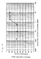
- Fig. 2 is a characteristic diagram showing relationships between gas pressure and the minimum breakdown electric fields generated at thick dielectric coating, thin dielectric coating, and bare electrode as basic data of the invention.
- Fig. 1 illustrates the gas-insulated switchgear in the first embodiment according to the invention, particularly showing a connection between parts.
- an insulating spacer 3 is used to connect one and the other earth metal containers 1, and one and the other high-voltage conductors 2.
- Shielding electrodes 6 having a larger diameter than that of the high-voltage conductors 2 are also provided to reduce electric field at live contacts 4, which form an electric path at the connection, and an embedded energizing electrode 5 of the insulating spacer 3.
- Shield coverings 6a are provided on the shielding electrodes 6 which produce electric field shield SH to form the outer peripheries of the shielding electrodes 6.
- the high-voltage conductors 2 provide high-voltage conductor sections CN.
- the shielding electrodes 6 are disposed at the portions where relatively high intensity electric field including the maximum electric field is generated, and have a relatively large diameter so as to decrease the electric field intensity.
- the high-voltage conductors 2 are disposed at the portion where relatively low intensity electric field is generated, and have a relatively small diameter.
- Insulating gas 7 sealed within the earth metal container 1 and the insulating spacer 3 insulate the high voltage area of the gas-insulated switchgear from the earth potential.
- the outer surfaces of the shielding electrodes 6 having the shield coverings 6a and the high-voltage conductors 2 are covered with thick dielectric coatings 8 and thin dielectric coatings 9, respectively.
- Fig. 2 compares the minimum breakdown electric field of the bare electrode with the minimum breakdown electric fields of the thick dielectric coating 8 and the thin dielectric coating 9. This figure includes the theoretical value of the breakdown electric field of SF 6 gas for reference.
- the ratio of the minimum breakdown electric fields of the thick dielectric coating 8 to the thin dielectric coating 9 to the bare electrode is approximately 1.45:1.15:1.
- the breakdown electric fields of the shielding electrode 6 where the maximum electric field is generated and the high-voltage conductor 2 can be equalized by covering the shielding electrode 6 with the thick dielectric coating 8, which increases the dielectric strength of the shielding electrode 6 to about 1.45 times higher than that of the bare electrode, and by covering the surface of the high-voltage conductor 2 with the thin dielectric coating 9, which increases the dielectric strength of the high-voltage conductor 2 to about 1.15 times higher than that of the bare electrode. Accordingly, the optimum insulation design having a miniaturized structure of the entire device can be provided.
- the thick dielectric coating 8 is made of epoxy resin, fluorocarbon resin, phthalic resin, and other materials.
- the thin dielectric coating 9 is made of epoxy resin, fluorocarbon resin, or aluminum oxide (Al 2 O 3 ) produced by applying electrolytic oxidation treatment to aluminum alloy, phthalic resin, and other materials.
- the preferable dielectric coating 8 and dielectric coating 9 can be produced from these materials.
- SF 6 gas is used as the insulating gas sealed within the respective components.
- a single element of dried air, N 2 , CO 2 , O 2 , C-C 4 F 8 , CF 3 I, or others may be used, or two or a larger number of elements of these may be used as mixed gas.
- the gas-insulated equipment in the first embodiment according to the invention includes: the voltage-stressed areas to which predetermined voltage is applied; the conductive container as the earth metal container 1 for accommodating the voltage-stressed areas; and the insulating gas for electrically insulating the voltage-stressed areas.
- the voltage-stressed areas are constituted by the shielding electrodes 6 and the high-voltage conductors 2.
- the shielding electrodes 6 produce the electric field shield SH and have the shield coverings 6a.
- the high-voltage conductors 2 form the high-voltage section CN.
- the first voltage-receiving portions of the voltage-stressed areas are formed by the shielding electrodes 6 which produce the electric field shield SH and have shield coverings 6a.
- the first voltage-receiving portions are coated with the relatively thick dielectric coatings 8.
- the second voltage-receiving portions at least as a part of the voltage-stressed areas other than the first voltage receiving portions including the shielding electrodes 6 which produce the electric field shield SH and have the shield coverings 6a, at which portions lower electric field than that at the first voltage-receiving portions is generated, are formed by the high-voltage conductors 2 which form the high-voltage section CN.
- the second voltage-receiving portions are coated with the relatively thin dielectric coatings 9.
- dielectric strength of the entire voltage-stressed area of the gas-insulated equipment can be efficiently improved, considering electric field distribution of this area and improving insulation coordination. Accordingly, the entire structure of the gas-insulated equipment provided according to this embodiment can be miniaturized.
- the relatively thick dielectric coatings 8 applied to the shielding electrodes 6 as the first voltage-receiving portions which form the electric field shielding SH and have the shield coverings 6a are made of epoxy resin or fluorocarbon resin
- the relatively thin dielectric coatings 9 applied to the second voltage-receiving portions are made of epoxy resin, fluorocarbon resin, or aluminum oxide (Al 2 O 3 ) produced by applying electrolytic oxidation treatment to aluminum alloy in the above structure.
- the insulating gas for electrically insulating the shielding electrodes 6 as the voltage-receiving portion which form the electric field shield SH and have the shielding coverings 6a and the high-voltage conductors 2 as the voltage receiving portion which form the high-voltage section CN is constituted by a single element of SF 6 gas, dried air, N 2 , CO 2 , O 2 , C-C 4 F B , CF 3 I, or others, or two or a larger number of these elements as mixed gas in the above structure.
- dielectric strength of the entire voltage-stressed areas of the gas-insulated equipment can be efficiently improved, considering electric field distribution of these areas and improving insulation coordination. Accordingly, the gas-insulated equipment provided according to this embodiment securely obtains appropriate gas insulation in the compact entire structure.
- Fig. 3 is a cross-sectional view showing a structure of a gas-insulated switchgear in the second embodiment according to the invention.
- Fig. 4 is a characteristic diagram showing the relationship between breakdown electric field at an electrode covered with dielectric coating and the thickness of the dielectric coating as basic data for the invention.
- Fig. 5 is a diagram showing dependency of breakdown electric field at an electrode on effective electrode area used as reference data for explaining advantages of the invention (quoted from the Electricity Society: Electric Discharge Handbook, Ohmsha, 1998 ).
- Figs. 6A and 6B are cross-sectional views showing a structure example of a gas-insulated switchgear. In Figs.
- Fig. 6A is a cross-sectional view of the entire structure
- Fig. 6B is a partial enlarged view.
- connection between parts with the insulating spacer 3 interposed therebetween in the gas-insulated switchgear is shown as an example.
- the connection can be used in the respective components of the gas-insulated switchgear including a cutoff breaker (CB) 10, a disconnecting switch (DS) 11, an earth switch (ES) 12, an instrument current transformer (CT) 13, a lightning arrestor (LA) 14, a main bus (BUS) 15, and others in the second embodiment as illustrated in Fig. 3 .
- CB cutoff breaker
- DS disconnecting switch
- ES earth switch
- CT instrument current transformer
- LA lightning arrestor
- BUS main bus
- the thick dielectric coating 8 is applied to the earth potential electrode. Since the maximum electric field is generated at this area, this invention is effectively applied. Thus, the thick dielectric coating 8 can be effectively applied to a portion at which higher electric field is generated than that generated at the high-voltage conductor 2 even on the earth potential side.
- the thin dielectric coating 9 can be effectively applied to the inner surface of the earth metal container 1.
- gas-insulated swtchgear with three-phase enclosure type busbar is shown in Fig. 3
- the invention is similarly applicable to entire three-phase packaged type and single-phase enclosure type gas-insulated switchgears.
- the thick dielectric coating 8 is made of epoxy resin, fluorocarbon resin, phthalic resin, and other materials.
- the thin dielectric coating 9 is made of epoxy resin, fluorocarbon resin, or aluminum oxide (Al 2 O 3 ) produced by applying electrolytic oxidation treatment to aluminum alloy, phthalic resin, and other materials similarly to the first embodiment.
- Fig. 4 shows the relationship between breakdown electric field of an electrode covered with dielectric coating and the thickness of the dielectric coating.
- the thickness of dielectric coating for producing superiority difference in breakdown electric field is approximately 1mm or larger for the thick film, and smaller than 1mm for the thin film.
- the coatings 8 and 9 may be smoothly connected with stepwise variation in the thickness of those so as to prevent discontinuous connection therebetween at the boundary and to equalize electric field distribution at the boundary.
- the insulating gas sealed within the respective components is not limited to SF 6 gas in this embodiment but may be constituted by a single element of dried air, N 2 , CO 2 , O 2 , C-C 4 F B , CF 3 I, or others, or two or a larger number of these elements as mixed gas.
- the gas-insulated equipment in the second embodiment according to the invention includes: the voltage-stressed areas to which predetermined voltage is applied; the conductive container as the earth metal container 1 for accommodating the voltage-stressed areas; and the insulating gas for electrically insulating the voltage-stressed areas.
- the voltage-stressed areas are constituted by the shielding electrodes 6 and the high-voltage conductors 2.
- the shielding electrodes 6 produce the electric field shield SH and have shield coverings 6a.
- the high-voltage conductors 2 form the high-voltage section CN.
- the first voltage-receiving portions of the voltage-stressed areas are formed by the shielding electrodes 6 which produce the electric field shield SH and have shield coverings 6a.
- the first voltage-receiving portions are coated with the relatively thick dielectric coatings 8.
- the second voltage-receiving portions at least as a part of the voltage-stressed areas other than the first voltage receiving portions including the shielding electrodes 6 which produce the electric field shield SH and have the shield coverings 6a, at which portions lower electric field than that at the first voltage-receiving portions is generated, are formed by the high-voltage conductors 2 which produce the high-voltage section CN.
- the second voltage-receiving portions are coated with the relatively thin dielectric coatings 9.
- the thickness of the relatively thick dielectric coatings 8 applied to the first voltage-receiving portions formed by the shielding electrodes 6 which produce the electric field shield SH and have shield coverings 6a is 1mm or larger.
- the thickness of the relatively thin dielectric coatings 9 applied to the second voltage-receiving portions formed by the high-voltage conductors 2 which produce the high-voltage section CN is smaller than 1mm.
- the gas-insulated equipment in the second embodiment according to the invention includes: the voltage-stressed areas to which predetermined voltage is applied; the conductive container as the earth metal container 1 for accommodating the voltage-stressed areas; and the insulating gas for electrically insulating the voltage-stressed areas.
- the voltage-stressed areas are constituted by the shielding electrodes 6 and the high-voltage conductors 2.
- the shielding electrodes 6 produce the electric field shield SH and have shield coverings 6a.
- the high-voltage conductors 2 form the high-voltage section CN.
- the first voltage-receiving portions of the voltage-stressed areas are formed by the shielding electrodes 6 which produce the electric field shield SH and have shield coverings 6a.
- the first voltage-receiving portions are coated with the relatively thick dielectric coatings 8.
- the second voltage-receiving portions at least as a part of the voltage-stressed areas other than the first voltage receiving portions including the shielding electrodes 6 which produce the electric field shield SH and have the shield coverings 6a, at which portions lower electric field than that at the first voltage-receiving portions is generated, are formed by the high-voltage conductor 2 which produce the high-voltage section CN.
- the second voltage-receiving portions are coated with the relatively thin dielectric coatings 9.
- the relatively thick dielectric coatings 8 are applied to the entire surfaces of the voltage-receiving portions formed by the shielding electrodes 6 which produce the electric field shield SH and have shield coverings 6a, or 90% or larger parts of the voltage-receiving portions at which the maximum electric field is generated.
- the relatively- thin dielectric coatings 9 are applied to the rest of the voltage receiving portions.
- the thickness of the dielectric coatings is varied stepwise at the boundary between the relatively thick dielectric coatings 8 and the relatively thin dielectric coatings 9 so that those coatings can be smoothly connected in the structures of the two cases described immediately above.
- dielectric strength of the entire voltage-stressed areas of the gas-insulated equipment can be efficiently improved, considering electric field distribution of these areas and improving insulation coordination. Accordingly, the entire structure of the gas-insulated equipment provided according to this embodiment can be miniaturized with the electric field at the thickness boundary of the dielectric coatings equalized.
- the relatively thick dielectric coatings applied to the first voltage-receiving portions are made of epoxy resin or fluorocarbon resin
- the relatively thin dielectric coatings applied to the second voltage-receiving portions are made of epoxy resin, fluorocarbon resin, or aluminum oxide (Al 2 O 3 ) produced by applying electrolytic oxidation treatment to aluminum alloy in the structure described above.
- the insulating gas for electrically insulating the voltage-stressed areas is formed by a single element of SF 6 gas, dried air, N 2 , CO 2 , O 2 , C-C 4 F 8 , CF 3 I, or others, or two or a larger number of these elements as mixed gas in the structure described above.
- dielectric strength of the entire voltage-stressed areas of the gas-insulated equipment can be efficiently improved, considering electric field distribution of these areas and improving insulation coordination. Accordingly, the entire structure of the gas-insulated equipment, provided according to this embodiment can be miniaturized with gas-insulation securely obtained in an appropriate manner.
- the thick-film coatings are applied to the portions around which the maximum electric field is generated, and the thin-film coatings are applied to the portions including the surfaces of the high-voltage conductors other than the portions to which the thick-film coatings are applied.
- dielectric strength of the entire electrode system of the gas-insulated switchgear can be efficiently improved, considering electric field distribution of the respective shielding electrodes and conductors and improving insulation coordination. Accordingly, the entire structure of the gas-insulated switchgear can be miniaturized.
- the invention is applicable to a gas-insulating switchgear used for electric power applications which is considerably miniaturized, for example.
Landscapes
- Gas-Insulated Switchgears (AREA)
- Installation Of Bus-Bars (AREA)
Description
- The present invention relates to a gas-insulated equipment, and more particularly to a gas-insulated equipment such as a gas-insulated switchgear which is miniaturized through improvement in its insulation capability.
- A conventional gas-insulated switchgear has a connection between high-voltage conductors, and shielding electrodes having a larger diameter than that of the high-voltage conductors are provided at the connection to reduce electric field thereat. The maximum electric field is generated at the shielding electrodes, and the ratio of the maximum electric field intensity to the electric field intensity at the high-voltage conductors is generally about 1.25:1. For miniaturizing the gas-insulated switchgear, dielectric strength in the vicinity of the area at which the maximum electric field is generated needs to be increased, and a method of improving dielectric strength by covering the metal electrode surface in this area with thick dielectric coating has been disclosed (for example, see
JP-A-2004-222483 - According to the above related-art method, the dielectric strength of the thick dielectric coating is approximately 1.45 times larger than that of a bare electrode. However, since the ratio of the maximum electric field intensity of the shielding electrode to the electric field intensity of the high-voltage conductor is about 1.25:1 as mentioned above, the dielectric strength of the bare electrode high-voltage conductor is insufficient. Thus, improvement in the dielectric strength of the entire electrode system needed for miniaturization of the device cannot be attained.
- Borin V.N.; Bortnik 1. M. ,,Dielectric coatings for gas-insulated high-voltage equipment" Sixth International conference on gas discharges and their applications, Vol. 1, 1980, pages 208-209, is considered as the closest prior art and discusses the features given in the preamble of
claim 1. - The present invention provides a gas-insulated device in accordance with
independent claim 1. Further preferred embodiments are given in the dependent claims. - The claimed invention can be better understood in view of the embodiments described hereinafter. In general, the described embodiments describe preferred embodiments of the invention. The attentive reader will note, however, that some aspects of the described embodiments extend beyond the scope of the claims. To the respect that the described embodiments indeed extend beyond the scope of the claims, the described embodiments are to be considered supplementary background information and do not constitute definitions of the invention per se. This also holds for the subsequent "Brief Description of the Drawings" as well as the "Description of the Preferred Embodiment".
-
-
Fig. 1 is a cross-sectional view of a gas-insulated switchgear in a first embodiment according to the invention; -
Fig. 2 is a characteristic diagram showing relationships between gas pressure and the minimum breakdown electric fields generated at thick dielectric coating, thin dielectric coating, and bare electrode as basic data for the invention; -
Fig. 3 is a cross-sectional view showing a structure of a gas-insulated switchgear in a second embodiment according to the invention; -
Fig. 4 is a characteristic diagram showing the relationship between breakdown electric field at an electrode covered with dielectric coating and the thickness of the dielectric coating as basic data for the invention; -
Fig. 5 shows dependency of breakdown electric field at an electrode on effective electrode area used as reference data for explaining advantages of the invention (quoted from the Electricity Society: Electric Discharge Handbook, Ohmsha, 1998); and -
Figs. 6A and 6B are cross-sectional views showing a structure example of a gas-insulated switchgear, where 90% or a larger part of the area at which the maximum electric field is generated is covered with thick dielectric coating, and the rest of the area is covered with thin dielectric coating, those two coatings being smoothly connected with stepwise variation in the thickness thereof at the boundary. - A first embodiment according to the invention is hereinafter described with reference to
Figs. 1 and2 .Fig. 1 is a-cross-sectional view of a structure of a gas-insulated switchgear in the first embodiment according to the invention.Fig. 2 is a characteristic diagram showing relationships between gas pressure and the minimum breakdown electric fields generated at thick dielectric coating, thin dielectric coating, and bare electrode as basic data of the invention. -
Fig. 1 illustrates the gas-insulated switchgear in the first embodiment according to the invention, particularly showing a connection between parts. In this example, aninsulating spacer 3 is used to connect one and the otherearth metal containers 1, and one and the other high-voltage conductors 2.Shielding electrodes 6 having a larger diameter than that of the high-voltage conductors 2 are also provided to reduce electric field atlive contacts 4, which form an electric path at the connection, and an embedded energizingelectrode 5 of theinsulating spacer 3. -
Shield coverings 6a are provided on theshielding electrodes 6 which produce electric field shield SH to form the outer peripheries of theshielding electrodes 6. The high-voltage conductors 2 provide high-voltage conductor sections CN. Theshielding electrodes 6 are disposed at the portions where relatively high intensity electric field including the maximum electric field is generated, and have a relatively large diameter so as to decrease the electric field intensity. The high-voltage conductors 2 are disposed at the portion where relatively low intensity electric field is generated, and have a relatively small diameter. - Insulating
gas 7 sealed within theearth metal container 1 and theinsulating spacer 3 insulate the high voltage area of the gas-insulated switchgear from the earth potential. The outer surfaces of theshielding electrodes 6 having the shield coverings 6a and the high-voltage conductors 2 are covered with thickdielectric coatings 8 and thindielectric coatings 9, respectively. -
Fig. 2 compares the minimum breakdown electric field of the bare electrode with the minimum breakdown electric fields of the thickdielectric coating 8 and the thindielectric coating 9. This figure includes the theoretical value of the breakdown electric field of SF6 gas for reference. - As apparent from
Fig. 2 , the ratio of the minimum breakdown electric fields of the thickdielectric coating 8 to the thindielectric coating 9 to the bare electrode is approximately 1.45:1.15:1. Thus, when the ratio of the maximum electric field intensity of theshielding electrode 6 to the electric field intensity of the high-voltage conductor 2 is about 1.25:1, the breakdown electric fields of theshielding electrode 6 where the maximum electric field is generated and the high-voltage conductor 2 can be equalized by covering theshielding electrode 6 with the thickdielectric coating 8, which increases the dielectric strength of theshielding electrode 6 to about 1.45 times higher than that of the bare electrode, and by covering the surface of the high-voltage conductor 2 with the thindielectric coating 9, which increases the dielectric strength of the high-voltage conductor 2 to about 1.15 times higher than that of the bare electrode. Accordingly, the optimum insulation design having a miniaturized structure of the entire device can be provided. - In the first embodiment, the thick
dielectric coating 8 is made of epoxy resin, fluorocarbon resin, phthalic resin, and other materials. The thindielectric coating 9 is made of epoxy resin, fluorocarbon resin, or aluminum oxide (Al2O3) produced by applying electrolytic oxidation treatment to aluminum alloy, phthalic resin, and other materials. The preferabledielectric coating 8 anddielectric coating 9 can be produced from these materials. - In this embodiment, SF6 gas is used as the insulating gas sealed within the respective components. However, a single element of dried air, N2, CO2, O2, C-C4F8, CF3I, or others may be used, or two or a larger number of elements of these may be used as mixed gas.
- The gas-insulated equipment in the first embodiment according to the invention includes: the voltage-stressed areas to which predetermined voltage is applied; the conductive container as the
earth metal container 1 for accommodating the voltage-stressed areas; and the insulating gas for electrically insulating the voltage-stressed areas. The voltage-stressed areas are constituted by theshielding electrodes 6 and the high-voltage conductors 2. Theshielding electrodes 6 produce the electric field shield SH and have theshield coverings 6a. The high-voltage conductors 2 form the high-voltage section CN. The first voltage-receiving portions of the voltage-stressed areas, at which portions relatively high electric field including the maximum electric field is generated, are formed by theshielding electrodes 6 which produce the electric field shield SH and haveshield coverings 6a. The first voltage-receiving portions are coated with the relatively thickdielectric coatings 8. The second voltage-receiving portions at least as a part of the voltage-stressed areas other than the first voltage receiving portions including theshielding electrodes 6 which produce the electric field shield SH and have theshield coverings 6a, at which portions lower electric field than that at the first voltage-receiving portions is generated, are formed by the high-voltage conductors 2 which form the high-voltage section CN. The second voltage-receiving portions are coated with the relatively thindielectric coatings 9. Thus, dielectric strength of the entire voltage-stressed area of the gas-insulated equipment can be efficiently improved, considering electric field distribution of this area and improving insulation coordination. Accordingly, the entire structure of the gas-insulated equipment provided according to this embodiment can be miniaturized. - In the first embodiment according to the invention, the relatively thick
dielectric coatings 8 applied to theshielding electrodes 6 as the first voltage-receiving portions which form the electric field shielding SH and have theshield coverings 6a, are made of epoxy resin or fluorocarbon resin, and the relatively thindielectric coatings 9 applied to the second voltage-receiving portions are made of epoxy resin, fluorocarbon resin, or aluminum oxide (Al2O3) produced by applying electrolytic oxidation treatment to aluminum alloy in the above structure. Thus, dielectric strength of the entire voltage-stressed areas of the gas-insulated equipment can be efficiently improved, considering electric field distribution of these areas and improving insulation coordination. Accordingly, the gas-insulated equipment provided according to this embodiment has preferable dielectric coatings in the compact entire structure. - In the first embodiment according to the invention, the insulating gas for electrically insulating the shielding
electrodes 6 as the voltage-receiving portion which form the electric field shield SH and have the shieldingcoverings 6a and the high-voltage conductors 2 as the voltage receiving portion which form the high-voltage section CN is constituted by a single element of SF6gas, dried air, N2, CO2, O2, C-C4FB, CF3I, or others, or two or a larger number of these elements as mixed gas in the above structure. Thus, dielectric strength of the entire voltage-stressed areas of the gas-insulated equipment can be efficiently improved, considering electric field distribution of these areas and improving insulation coordination. Accordingly, the gas-insulated equipment provided according to this embodiment securely obtains appropriate gas insulation in the compact entire structure. - A second embodiment according to the invention is now described with reference to
Figs. 3 through 6 .Fig. 3 is a cross-sectional view showing a structure of a gas-insulated switchgear in the second embodiment according to the invention.Fig. 4 is a characteristic diagram showing the relationship between breakdown electric field at an electrode covered with dielectric coating and the thickness of the dielectric coating as basic data for the invention.Fig. 5 is a diagram showing dependency of breakdown electric field at an electrode on effective electrode area used as reference data for explaining advantages of the invention (quoted from the Electricity Society: Electric Discharge Handbook, Ohmsha, 1998).Figs. 6A and 6B are cross-sectional views showing a structure example of a gas-insulated switchgear. InFigs. 6A and 6B , 90% of a larger part of the area at which the maximum electric field is generated is covered with thick dielectric coating, and the rest of the area is covered with thin dielectric coating. Those two coatings are smoothly connected with stepwise variation in the thickness of the coatings at the boundary.Fig. 6A is a cross-sectional view of the entire structure, andFig. 6B is a partial enlarged view. - In the first embodiment, the connection between parts with the insulating
spacer 3 interposed therebetween in the gas-insulated switchgear is shown as an example. However, the connection can be used in the respective components of the gas-insulated switchgear including a cutoff breaker (CB) 10, a disconnecting switch (DS) 11, an earth switch (ES) 12, an instrument current transformer (CT) 13, a lightning arrestor (LA) 14, a main bus (BUS) 15, and others in the second embodiment as illustrated inFig. 3 . - As shown in
Fig. 3 , large-diameter shielding electrodes at which the maximum electric field is generated are covered with the thickdielectric coatings 8, and high-voltage conductor sections as the live parts of the main circuit having a smaller diameter than that of the shielding electrodes are covered by the thindielectric coatings 9 in the respective components. Thus, the insulation design of the entire gas-insulated switchgear is optimized, allowing its structure to be made compact. The insulation design can be rationalized when the maximum electric fields of the respective components are set at the same intensity. - As for the earth switch (ES) 12, the thick
dielectric coating 8 is applied to the earth potential electrode. Since the maximum electric field is generated at this area, this invention is effectively applied. Thus, the thickdielectric coating 8 can be effectively applied to a portion at which higher electric field is generated than that generated at the high-voltage conductor 2 even on the earth potential side. When high electric field, though not the maximum, is generated on the earth potential side such as the inner surface of theearth metal container 1 in the respective components of the gas-insulated switchgear which has been further miniaturized, the thindielectric coating 9 can be effectively applied to the inner surface of theearth metal container 1. - While the gas-insulated swtchgear with three-phase enclosure type busbar is shown in
Fig. 3 , the invention is similarly applicable to entire three-phase packaged type and single-phase enclosure type gas-insulated switchgears. - In the second embodiment, the thick
dielectric coating 8 is made of epoxy resin, fluorocarbon resin, phthalic resin, and other materials. The thindielectric coating 9 is made of epoxy resin, fluorocarbon resin, or aluminum oxide (Al2O3) produced by applying electrolytic oxidation treatment to aluminum alloy, phthalic resin, and other materials similarly to the first embodiment. -
Fig. 4 shows the relationship between breakdown electric field of an electrode covered with dielectric coating and the thickness of the dielectric coating. As apparent from the figure, the thickness of dielectric coating for producing superiority difference in breakdown electric field is approximately 1mm or larger for the thick film, and smaller than 1mm for the thin film. - As shown in
Fig. 5 , it is known that breakdown electric field at an electrode exhibits large dependency on the electrode area where the maximum electric field is generated within the range of 90% of that area (effective electrode area S90%). Thus, the entire surfaces of the respective shielding electrodes as shown inFig. 1 , or the 90% or a larger part of the area where the maximum electric field is generated may be covered with the thickdielectric coatings 8, and the rest of the area may be covered with the thindielectric coatings 9 as shown inFig. 6 . When the thickdielectric coating 8 and the thindielectric coating 9 are co-used for thesame shielding electrode 6 as in this case, thecoatings - The insulating gas sealed within the respective components is not limited to SF6 gas in this embodiment but may be constituted by a single element of dried air, N2, CO2, O2, C-C4FB, CF3I, or others, or two or a larger number of these elements as mixed gas.
- The gas-insulated equipment in the second embodiment according to the invention includes: the voltage-stressed areas to which predetermined voltage is applied; the conductive container as the
earth metal container 1 for accommodating the voltage-stressed areas; and the insulating gas for electrically insulating the voltage-stressed areas. The voltage-stressed areas are constituted by the shieldingelectrodes 6 and the high-voltage conductors 2. The shieldingelectrodes 6 produce the electric field shield SH and haveshield coverings 6a. The high-voltage conductors 2 form the high-voltage section CN. The first voltage-receiving portions of the voltage-stressed areas, at which portions relatively high electric field including the maximum electric field is generated, are formed by the shieldingelectrodes 6 which produce the electric field shield SH and haveshield coverings 6a. The first voltage-receiving portions are coated with the relatively thickdielectric coatings 8. The second voltage-receiving portions at least as a part of the voltage-stressed areas other than the first voltage receiving portions including theshielding electrodes 6 which produce the electric field shield SH and have theshield coverings 6a, at which portions lower electric field than that at the first voltage-receiving portions is generated, are formed by the high-voltage conductors 2 which produce the high-voltage section CN. The second voltage-receiving portions are coated with the relatively thindielectric coatings 9. The thickness of the relatively thickdielectric coatings 8 applied to the first voltage-receiving portions formed by the shieldingelectrodes 6 which produce the electric field shield SH and haveshield coverings 6a is 1mm or larger. The thickness of the relatively thindielectric coatings 9 applied to the second voltage-receiving portions formed by the high-voltage conductors 2 which produce the high-voltage section CN is smaller than 1mm. Thus, by the thick and thin dielectric coatings having the predetermined thickness, dielectric strength of the entire voltage-stressed areas of the gas-insulated equipment can be efficiently improved, considering electric field distribution of these areas and improving insulation coordination. Accordingly, the entire structure of the gas-insulated equipment provided according to this embodiment can be miniaturized. - The gas-insulated equipment in the second embodiment according to the invention includes: the voltage-stressed areas to which predetermined voltage is applied; the conductive container as the
earth metal container 1 for accommodating the voltage-stressed areas; and the insulating gas for electrically insulating the voltage-stressed areas. The voltage-stressed areas are constituted by the shieldingelectrodes 6 and the high-voltage conductors 2. The shieldingelectrodes 6 produce the electric field shield SH and haveshield coverings 6a. The high-voltage conductors 2 form the high-voltage section CN. The first voltage-receiving portions of the voltage-stressed areas, at which portions relatively high electric field including the maximum electric field is generated, are formed by the shieldingelectrodes 6 which produce the electric field shield SH and haveshield coverings 6a. The first voltage-receiving portions are coated with the relatively thickdielectric coatings 8. The second voltage-receiving portions at least as a part of the voltage-stressed areas other than the first voltage receiving portions including theshielding electrodes 6 which produce the electric field shield SH and have theshield coverings 6a, at which portions lower electric field than that at the first voltage-receiving portions is generated, are formed by the high-voltage conductor 2 which produce the high-voltage section CN. The second voltage-receiving portions are coated with the relatively thindielectric coatings 9. The relatively thickdielectric coatings 8 are applied to the entire surfaces of the voltage-receiving portions formed by the shieldingelectrodes 6 which produce the electric field shield SH and haveshield coverings 6a, or 90% or larger parts of the voltage-receiving portions at which the maximum electric field is generated. The relatively-thin dielectric coatings 9 are applied to the rest of the voltage receiving portions. Thus, by limiting the areas to which the thick dielectric coatings are applied, dielectric strength of the entire voltage-stressed areas of the gas-insulated equipment can be efficiently improved, considering electric field distribution of these areas and improving insulation coordination. Accordingly, the entire structure of the gas-insulated equipment provided according to this embodiment can be miniaturized. - In the second embodiment according to the invention, the thickness of the dielectric coatings is varied stepwise at the boundary between the relatively thick
dielectric coatings 8 and the relatively thindielectric coatings 9 so that those coatings can be smoothly connected in the structures of the two cases described immediately above. Thus, dielectric strength of the entire voltage-stressed areas of the gas-insulated equipment can be efficiently improved, considering electric field distribution of these areas and improving insulation coordination. Accordingly, the entire structure of the gas-insulated equipment provided according to this embodiment can be miniaturized with the electric field at the thickness boundary of the dielectric coatings equalized. - In the second embodiment according to the invention, the relatively thick dielectric coatings applied to the first voltage-receiving portions are made of epoxy resin or fluorocarbon resin, and the relatively thin dielectric coatings applied to the second voltage-receiving portions are made of epoxy resin, fluorocarbon resin, or aluminum oxide (Al2O3) produced by applying electrolytic oxidation treatment to aluminum alloy in the structure described above. Thus, dielectric strength of the entire voltage-stressed areas of the gas-insulated equipment can be efficiently improved, considering electric field distribution of these areas and improving insulation coordination. Accordingly, the entire structure of the gas-insulated equipment provided according to this embodiment can be miniaturized with the preferable dielectric coatings formed.
- In the second embodiment according to the invention, the insulating gas for electrically insulating the voltage-stressed areas is formed by a single element of SF6 gas, dried air, N2, CO2, O2, C-C4F8, CF3I, or others, or two or a larger number of these elements as mixed gas in the structure described above. Thus, dielectric strength of the entire voltage-stressed areas of the gas-insulated equipment can be efficiently improved, considering electric field distribution of these areas and improving insulation coordination. Accordingly, the entire structure of the gas-insulated equipment, provided according to this embodiment can be miniaturized with gas-insulation securely obtained in an appropriate manner.
- The following structures in (1) through (6) are proposed according to the invention:
- (1) A gas-insulated switchgear which includes: insulating gas sealed within an earth metal container; an insulating spacer for insulating and supporting high-voltage conductors; and electrodes for electrically shielding live contacts which provide electrical connection between parts and an embedded energizing electrode of the insulating spacer, characterized in that: the portions of the electrodes at which the maximum electric field is generated are covered with thick dielectric coatings; and the portions of the electrodes at which high electric field is generated other than the above portions and the high-voltage conductors are covered with thin dielectric coatings.
- (2) A gas-insulated switchgear according to (1), characterized in that: the thick dielectric coatings are made of epoxy resin or fluorocarbon resin, and the thin dielectric coatings are made of epoxy resin, fluorocarbon resin, or aluminum oxide (Al2O3) produced by applying electrolytic oxidation treatment to aluminum alloy.
- (3) A gas-insulated switchgear according to (1) or (2), characterized in that: the thickness of the thick dielectric coatings is 1mm or larger; and the thickness of the thin dielectric coatings is smaller than 1mm.
- (4) A gas-insulated switchgear according to any one of (1) through (3), characterized in that: the thick dielectric coatings are applied to the entire surfaces or 90% or larger parts of the electrodes at which the maximum electric field is generated; and the thin dielectric coatings are applied to the remaining parts of the electrodes at which the maximum electric field is generated.
- (5) A gas-insulated switchgear according to (4), characterized in that the thickness of the dielectric coatings is varied stepwise at the boundary between the thick dielectric coatings and the thin dielectric coatings on the same electrode so that those coatings can be smoothly connected.
- (6) A gas-insulated switchgear according to any one of (1) through (5), characterized in that: the insulating gas is formed by a single element of SF6 gas, dried air, N2, CO2, O2, C-C4F8, CF3I, or others, or two or a larger number of these elements as mixed gas.
- According to the invention, the thick-film coatings are applied to the portions around which the maximum electric field is generated, and the thin-film coatings are applied to the portions including the surfaces of the high-voltage conductors other than the portions to which the thick-film coatings are applied. Thus, dielectric strength of the entire electrode system of the gas-insulated switchgear can be efficiently improved, considering electric field distribution of the respective shielding electrodes and conductors and improving insulation coordination. Accordingly, the entire structure of the gas-insulated switchgear can be miniaturized.
- The invention is applicable to a gas-insulating switchgear used for electric power applications which is considerably miniaturized, for example.
Claims (6)
- A gas-insulated device, comprising:an earth metal container (1) with earth potential;insulating gas (7) sealed within the earth metal container;a high-voltage conductor (2) disposed in the earth metal container (1);a shielding electrode (6) disposed in the earth metal container (1) and connected to the high-voltage conductor (2); andan insulating spacer (3);wherein the high-voltage conductor (2) and the shielding electrode (6) are insulated from the earth metal container (1) by the insulating spacer (3) and the insulating gas (7);the shielding electrode (6) have a larger diameter than that of the high-voltage conductors (2);characterised in that:the shielding electrode (6) is covered with relatively thick dielectric coatings (8) as compared with the high-voltage conductor (2) which is covered with relatively thin dielectric coatings (9);each thickness of the relatively thick dielectric coatings (8) and the relatively thin dielectric coatings (9) is such a thickness that breakdown electric fields of the shielding electrode (6) and the high-voltage conductor (2) are equalized.
- A gas-insulated device according to claim 1, wherein the thickness of the relatively thick film dielectric coatings (8) applied to the shielding electrode (6) is 1mm or larger;
and the thickness of the relatively thin film dielectric coatings (9) applied to the high-voltage conductor (2) is smaller then 1mm. - A gas-insulated device according to claims 1 or 2, wherein the relatively thick film dielectric coatings (8) are applied to the entire surfaces or 90% or larger parts of the shielding electrode (6) at which the maximum electric field is generated; and
the relatively thin film dielectric coatings (9) are applied to the rest of the shielding electrode (6) at which the maximum electric field is generated. - A gas-insulated device according to any one of claims 1 through 3, wherein the thickness of the dielectric coatings is varied stepwise at the boundary between the relatively thick film dielectric coatings (8) and the relatively thin dielectric coatings (9) so that those coatings can be smoothly connected.
- A gas-insulated device according to any one of claims 1 through 4, wherein the relatively thick dielectric coatings (8) applied to the shielding electrode (6) are made of epoxy resin or fluorocarbon resin, and the relatively thin dielectric coatings (9) applied to the high-voltage conductor (2) are made of epoxy resin, fluorocarbon resin, or aluminum oxide (Al2O3) produced by applying electrolytic oxidation treatment to aluminium alloy.
- A gas-insulated device according to any one of claims 1 through 6, wherein the insulating gas (7) for electrically insulating the voltage-receiving areas is formed by a single element of SF6 gas, dried air, N2, CO2, O2, C-C4F8, CF3l, or others, or two or a larger number of these elements as mixed gas.
Applications Claiming Priority (2)
| Application Number | Priority Date | Filing Date | Title |
|---|---|---|---|
| JP2005142057A JP4429205B2 (en) | 2005-05-16 | 2005-05-16 | Gas insulation equipment |
| EP06010100.3A EP1724802B1 (en) | 2005-05-16 | 2006-05-16 | Gas-insulated equipment |
Related Parent Applications (2)
| Application Number | Title | Priority Date | Filing Date |
|---|---|---|---|
| EP06010100.3A Division-Into EP1724802B1 (en) | 2005-05-16 | 2006-05-16 | Gas-insulated equipment |
| EP06010100.3 Division | 2006-05-16 |
Publications (3)
| Publication Number | Publication Date |
|---|---|
| EP2214191A2 EP2214191A2 (en) | 2010-08-04 |
| EP2214191A3 EP2214191A3 (en) | 2010-09-22 |
| EP2214191B1 true EP2214191B1 (en) | 2011-12-07 |
Family
ID=36809138
Family Applications (2)
| Application Number | Title | Priority Date | Filing Date |
|---|---|---|---|
| EP10162099A Ceased EP2214191B1 (en) | 2005-05-16 | 2006-05-16 | Gas-insulated equipment |
| EP06010100.3A Ceased EP1724802B1 (en) | 2005-05-16 | 2006-05-16 | Gas-insulated equipment |
Family Applications After (1)
| Application Number | Title | Priority Date | Filing Date |
|---|---|---|---|
| EP06010100.3A Ceased EP1724802B1 (en) | 2005-05-16 | 2006-05-16 | Gas-insulated equipment |
Country Status (4)
| Country | Link |
|---|---|
| US (2) | US7742283B2 (en) |
| EP (2) | EP2214191B1 (en) |
| JP (1) | JP4429205B2 (en) |
| CN (1) | CN1897377B (en) |
Families Citing this family (51)
| Publication number | Priority date | Publication date | Assignee | Title |
|---|---|---|---|---|
| JP4429205B2 (en) * | 2005-05-16 | 2010-03-10 | 三菱電機株式会社 | Gas insulation equipment |
| JPWO2007032344A1 (en) * | 2005-09-15 | 2009-03-19 | 学校法人東京電機大学 | Gas insulated switchgear and gas circuit breaker |
| EP2015414B1 (en) * | 2006-12-21 | 2016-08-17 | Mitsubishi Electric Corporation | Gas insulated switchgear |
| EP1983623A1 (en) * | 2007-04-18 | 2008-10-22 | Eaton Electric B.V. | Cooling arrangement for conductor in electrical installation |
| JP4949919B2 (en) * | 2007-04-24 | 2012-06-13 | 三菱電機株式会社 | Gas insulated electrical equipment |
| JP4940020B2 (en) * | 2007-05-24 | 2012-05-30 | 三菱電機株式会社 | Gas insulated switchgear |
| JP4919882B2 (en) * | 2007-06-21 | 2012-04-18 | 三菱電機株式会社 | Electrical equipment |
| JP5198989B2 (en) * | 2008-03-18 | 2013-05-15 | 一般財団法人電力中央研究所 | Conductor connection device for gas insulated power equipment |
| JP5135129B2 (en) * | 2008-08-29 | 2013-01-30 | 株式会社東芝 | Gas insulation equipment |
| US8520368B2 (en) * | 2008-09-11 | 2013-08-27 | Mitsubishi Electric Corporation | Gas insulated switchgear |
| AU2009347593B2 (en) | 2009-06-12 | 2015-01-15 | Abb Technology Ag | Dielectric insulation medium |
| DE202009009305U1 (en) | 2009-06-17 | 2009-11-05 | Ormazabal Gmbh | Switching device for medium, high or very high voltage with a filling medium |
| EP3553905B1 (en) * | 2009-07-17 | 2021-02-17 | Mitsubishi Electric Corporation | Gas-insulated bus |
| DE102009051769A1 (en) * | 2009-10-29 | 2011-05-05 | Siemens Aktiengesellschaft | Electrical energy transmission device, has encapsulated housing that surrounds power current path, where surface of housing turned towards path exhibits coatings with smaller electrical conductivity than housing section that forms surface |
| FR2955970B1 (en) * | 2010-02-02 | 2012-03-09 | Areva T & D Sas | USE OF GASEOUS FLUOROCETONES FOR ELECTRICAL INSULATION AND / OR EXTINGUISHING ELECTRICAL ARC |
| JP5395038B2 (en) * | 2010-11-19 | 2014-01-22 | 三菱電機株式会社 | Gas insulated electrical equipment |
| EP2652751B1 (en) | 2010-12-14 | 2015-02-25 | ABB Research Ltd. | Dielectric insulation medium |
| RU2621900C2 (en) | 2010-12-14 | 2017-06-08 | Абб Текнолоджи Аг | Dielectric insulating medium |
| CA2821158A1 (en) | 2010-12-16 | 2012-06-21 | Abb Technology Ag | Dielectric insulation medium |
| JP4781493B1 (en) * | 2011-02-28 | 2011-09-28 | 三菱電機株式会社 | Gas insulated bus |
| CN103534888B (en) * | 2011-04-08 | 2015-09-23 | 三菱电机株式会社 | Gas-insulated switchgear device |
| FR2975821B1 (en) | 2011-05-24 | 2013-07-05 | Alstom Grid Sas | MIXTURE OF DECAFLUORO-2-METHYLBUTAN-3-ONE AND A VECTOR GAS AS A MEDIUM OF ELECTRICAL ISOLATION AND / OR EXTINGUISHING ELECTRIC ARCS IN HIGH VOLTAGE |
| FR2975836B1 (en) | 2011-05-24 | 2014-07-04 | Schneider Electric Ind Sas | ELECTRICAL GAS-INSULATING APPARATUS HAVING MEANS FOR CONTROLLING GAS PRESSURE |
| FR2975820B1 (en) | 2011-05-24 | 2013-07-05 | Schneider Electric Ind Sas | MIXTURE OF DECAFLUORO-2-METHYLBUTAN-3-ONE AND A VECTOR GAS AS A MEDIUM ELECTRICAL INSULATION AND / OR EXTINGUISHING ELECTRIC ARCS AT MEDIUM VOLTAGE |
| FR2977708B1 (en) | 2011-07-05 | 2014-05-23 | Alstom Grid Sas | USE OF HYDROFLUOROOLEFIN AS A HIGH VOLTAGE ARC INSULATION AND / OR EXTINGUISHMENT MEDIUM AND HIGH VOLTAGE ELECTRICAL GAS INSULATING DEVICE COMPRISING SAME |
| FR2977707B1 (en) | 2011-07-05 | 2014-05-23 | Schneider Electric Ind Sas | USE OF HYDROFLUOROOLEFIN AS A MEDIUM VOLTAGE ARC INSULATION AND / OR EXTINGUISHMENT MEDIUM AND GAS INSULATED MEDIUM VOLTAGE ELECTRICAL APPARATUS COMPRISING SAME |
| FR2980628B1 (en) | 2011-09-22 | 2014-07-25 | Schneider Electric Ind Sas | MIXTURE OF HYDROFLUOROOLEFIN AND FLUOROCETONE FOR USE AS ARC INSULATION AND / OR EXTINGUISHING MEDIUM AND GAS ISOLATED MEDIUM VOLTAGE ELECTRICAL APPARATUS INCLUDING THE SAME |
| FR2980629B1 (en) | 2011-09-22 | 2015-01-16 | Alstom Grid Sas | MIXTURE OF HYDROFLUOROOLEFIN AND FLUOROCETONE FOR USE AS ARC INSULATION AND / OR EXTINGUISHING MEDIUM AND HIGH VOLTAGE ELECTRICAL GAS INSULATING DEVICE COMPRISING SAME |
| EP2600375A1 (en) * | 2011-11-30 | 2013-06-05 | Eaton Industries (Netherlands) B.V. | Driving rod for medium voltage switching element gear |
| FR2983340B1 (en) | 2011-11-30 | 2019-05-17 | Alstom Technology Ltd | POLYFLUORINATED OXIRANES AS GAS OF ELECTRICAL ISOLATION AND / OR EXTINGUISHING ELECTRIC ARCS IN HIGH VOLTAGE |
| WO2013087700A1 (en) | 2011-12-13 | 2013-06-20 | Abb Technology Ag | Sealed and gas insulated high voltage converter environment for offshore platforms |
| FR2986103B1 (en) | 2012-01-23 | 2015-03-06 | Alstom Technology Ltd | GASEOUS MEDIUM COMPRISING AT LEAST ONE POLYFLUORINE OXIRAN AND A HYDROFLUOROOLEFINE FOR THE ELECTRICAL INSULATION AND / OR THE EXTINGUISHING OF HIGH VOLTAGE ELECTRIC ARCS |
| FR2988215B1 (en) * | 2012-03-16 | 2014-02-28 | Schneider Electric Ind Sas | MIXTURE OF HYDROFLUOROOLEFIN AND HYDROFLUOROCARBIDE FOR IMPROVING INTERNAL ARC HOLDING IN MEDIUM AND HIGH VOLTAGE ELECTRIC APPLIANCES |
| CN108831587A (en) | 2012-04-04 | 2018-11-16 | 3M创新有限公司 | Fluorination nitrile as dielectric gaseous |
| FR2995462B1 (en) | 2012-09-10 | 2014-09-05 | Alstom Technology Ltd | MEDIUM OR HIGH VOLTAGE ELECTRICAL APPARATUS WITH LOW ENVIRONMENTAL IMPACT AND HYBRID INSULATION |
| US9508507B2 (en) * | 2012-12-21 | 2016-11-29 | Mitsubishi Electric Corporation | Gas insulated electrical equipment |
| WO2014112123A1 (en) * | 2013-01-21 | 2014-07-24 | 三菱電機株式会社 | Gas-insulated switchgear |
| FR3011138B1 (en) | 2013-09-20 | 2015-10-30 | Alstom Technology Ltd | GAS INSULATED MEDIUM OR HIGH VOLTAGE ELECTRICAL APPARATUS COMPRISING CARBON DIOXIDE, OXYGEN AND HEPTAFLUOROISOBUTYRONITRILE |
| FR3016746B1 (en) * | 2014-01-21 | 2017-12-15 | Alstom Technology Ltd | MEDIUM OR HIGH VOLTAGE ELECTRICAL APPARATUS WITH GAS INSULATION COMPRISING SULFUR HEXAFLUORIDE AND ANOTHER FLUORINE COMPOUND |
| WO2016006137A1 (en) * | 2014-07-10 | 2016-01-14 | 三菱電機株式会社 | Gas insulated electric device and gas insulated electric device manufacturing method |
| FR3027154B1 (en) | 2014-10-14 | 2016-11-25 | Arkema France | GAS ISOLATION OR EXTINGUISHING ELECTRIC ARCS |
| KR20160081365A (en) * | 2014-12-31 | 2016-07-08 | 주식회사 효성 | Electrode device for gas-insulated switchgear |
| FR3032828B1 (en) * | 2015-02-13 | 2017-03-17 | Alstom Technology Ltd | GAS INSULATED MEDIUM OR HIGH VOLTAGE ELECTRICAL APPARATUS COMPRISING HEPTAFLUOROISOBUTYRONITRILE AND TETRAFLUOROMETHANE |
| EP3188196B1 (en) * | 2015-12-28 | 2020-03-04 | General Electric Technology GmbH | Medium- or high-voltage thin electrical apparatus with hybrid insulation |
| WO2017163467A1 (en) * | 2016-03-24 | 2017-09-28 | 三菱電機株式会社 | Electric-appliance connecting device |
| FR3079359B1 (en) | 2018-03-22 | 2020-10-09 | Arkema France | USE OF 1-CHLORO-2,3,3,3-TETRAFLUOROPROPENE FOR INSULATING OR EXTINGUISHING ELECTRIC ARCS |
| FR3082993B1 (en) | 2018-06-25 | 2020-05-29 | Arkema France | USE OF TRIFLUOROETHYLENE FOR THE INSULATION OR EXTINGUISHING OF ELECTRIC ARCS |
| CN110649543A (en) * | 2018-06-26 | 2020-01-03 | 江苏中顺电气有限公司 | Power transmission bus |
| CN110183935A (en) * | 2019-06-04 | 2019-08-30 | 上海电气输配电试验中心有限公司 | New bar electrode surface coat preparation process in environmentally friendly gas |
| CN112685985B (en) * | 2020-12-29 | 2023-01-17 | 西北核技术研究所 | A Capacitor Design Method for Suppressing Surface Flashover |
| JP7831615B2 (en) * | 2022-09-07 | 2026-03-17 | 富士電機株式会社 | Switching device |
Family Cites Families (12)
| Publication number | Priority date | Publication date | Assignee | Title |
|---|---|---|---|---|
| JPH0393417A (en) * | 1989-09-04 | 1991-04-18 | Toshiba Corp | Insulation structure of gas insulated electric machine |
| JP3028975B2 (en) | 1991-07-22 | 2000-04-04 | 株式会社東芝 | Composite insulation bus |
| JP3437633B2 (en) * | 1994-03-31 | 2003-08-18 | 株式会社日立製作所 | Circuit breaker with parallel resistance |
| DE4427163A1 (en) * | 1994-08-01 | 1996-02-08 | Abb Management Ag | Gas pressure switch |
| DE19533794A1 (en) * | 1995-09-13 | 1997-03-20 | Abb Patent Gmbh | Metal-enclosed, gas-insulated high-voltage switch |
| JP3712456B2 (en) | 1996-01-16 | 2005-11-02 | 株式会社東芝 | Gas insulated disconnect switch |
| JPH09231885A (en) * | 1996-02-22 | 1997-09-05 | Hitachi Ltd | Gas circuit breaker |
| FR2751782B1 (en) * | 1996-07-23 | 1998-08-28 | Gec Alsthom T & D Sa | HIGH VOLTAGE CIRCUIT BREAKER WITH SELF-BLOWING ARC |
| FR2789798B1 (en) * | 1999-02-15 | 2004-01-09 | Alstom | SELF-DISCONNECTOR, MEDIUM VOLTAGE CIRCUIT-BREAKER MODULE AND CORRESPONDING POWER DISTRIBUTION STATION |
| JP3860553B2 (en) * | 2002-11-19 | 2006-12-20 | 三菱電機株式会社 | Gas insulated switchgear |
| TWI251847B (en) * | 2003-12-26 | 2006-03-21 | Hitachi Ltd | Vacuum switchgear system and kit for system |
| JP4429205B2 (en) * | 2005-05-16 | 2010-03-10 | 三菱電機株式会社 | Gas insulation equipment |
-
2005
- 2005-05-16 JP JP2005142057A patent/JP4429205B2/en not_active Expired - Fee Related
-
2006
- 2006-05-16 CN CN2006100998579A patent/CN1897377B/en not_active Expired - Fee Related
- 2006-05-16 EP EP10162099A patent/EP2214191B1/en not_active Ceased
- 2006-05-16 EP EP06010100.3A patent/EP1724802B1/en not_active Ceased
- 2006-05-16 US US11/434,218 patent/US7742283B2/en not_active Expired - Fee Related
-
2010
- 2010-03-10 US US12/720,842 patent/US7848084B2/en not_active Expired - Fee Related
Also Published As
| Publication number | Publication date |
|---|---|
| EP2214191A2 (en) | 2010-08-04 |
| JP4429205B2 (en) | 2010-03-10 |
| US7848084B2 (en) | 2010-12-07 |
| CN1897377A (en) | 2007-01-17 |
| EP1724802A2 (en) | 2006-11-22 |
| JP2006320156A (en) | 2006-11-24 |
| US20100165549A1 (en) | 2010-07-01 |
| CN1897377B (en) | 2011-08-31 |
| US20060254791A1 (en) | 2006-11-16 |
| HK1098257A1 (en) | 2007-07-13 |
| EP1724802A3 (en) | 2007-12-26 |
| US7742283B2 (en) | 2010-06-22 |
| EP1724802B1 (en) | 2014-03-19 |
| EP2214191A3 (en) | 2010-09-22 |
Similar Documents
| Publication | Publication Date | Title |
|---|---|---|
| EP1724802B1 (en) | Gas-insulated equipment | |
| US11901709B2 (en) | Gas-insulated switchgear | |
| JP2771505B2 (en) | DC bushing | |
| JPH1023620A (en) | Electric field relaxation device | |
| JP5324530B2 (en) | High voltage switchgear | |
| JP3744721B2 (en) | Flexible conductor and flexible connecting member | |
| JP2726537B2 (en) | Gas insulating spacer | |
| JP4931395B2 (en) | Insulation structure of electrical equipment and switchgear using the insulation structure | |
| JP3585517B2 (en) | Gas insulated bushing | |
| EP4443462B1 (en) | COMPACT SWITCHGEAR | |
| JP2004056927A (en) | Gas insulated switchgear | |
| JP7735358B2 (en) | Branch bus bar device | |
| JP7510395B2 (en) | Gas insulated switchgear | |
| HK1098257B (en) | Gas-insulated equipment | |
| CN111029207B (en) | Switchgear with arrangement for bushings | |
| JP3657890B2 (en) | Gas insulated switchgear | |
| RU2275708C1 (en) | Vacuum switch | |
| CN114694986A (en) | Switching device with reduced partial discharge and improved triple point characteristics | |
| WO2025013121A1 (en) | Insulation device | |
| Teixeria et al. | Insulation coordination of MV power cables | |
| JPH02223324A (en) | Gas insulating spacer | |
| JP2933747B2 (en) | Gas insulated switchgear | |
| JP3537985B2 (en) | Cable head and switch gear with cable head | |
| JPH0393417A (en) | Insulation structure of gas insulated electric machine | |
| JPH1094115A (en) | Through-type insulation support device |
Legal Events
| Date | Code | Title | Description |
|---|---|---|---|
| PUAI | Public reference made under article 153(3) epc to a published international application that has entered the european phase |
Free format text: ORIGINAL CODE: 0009012 |
|
| 17P | Request for examination filed |
Effective date: 20100506 |
|
| AC | Divisional application: reference to earlier application |
Ref document number: 1724802 Country of ref document: EP Kind code of ref document: P |
|
| AK | Designated contracting states |
Kind code of ref document: A2 Designated state(s): CH DE FR LI |
|
| PUAL | Search report despatched |
Free format text: ORIGINAL CODE: 0009013 |
|
| AK | Designated contracting states |
Kind code of ref document: A3 Designated state(s): CH DE FR LI |
|
| GRAP | Despatch of communication of intention to grant a patent |
Free format text: ORIGINAL CODE: EPIDOSNIGR1 |
|
| RIC1 | Information provided on ipc code assigned before grant |
Ipc: H01H 33/24 20060101AFI20110520BHEP Ipc: H02B 13/035 20060101ALI20110520BHEP |
|
| GRAS | Grant fee paid |
Free format text: ORIGINAL CODE: EPIDOSNIGR3 |
|
| GRAA | (expected) grant |
Free format text: ORIGINAL CODE: 0009210 |
|
| AC | Divisional application: reference to earlier application |
Ref document number: 1724802 Country of ref document: EP Kind code of ref document: P |
|
| AK | Designated contracting states |
Kind code of ref document: B1 Designated state(s): CH DE FR LI |
|
| REG | Reference to a national code |
Ref country code: CH Ref legal event code: EP |
|
| REG | Reference to a national code |
Ref country code: CH Ref legal event code: NV Representative=s name: TROESCH SCHEIDEGGER WERNER AG |
|
| REG | Reference to a national code |
Ref country code: DE Ref legal event code: R096 Ref document number: 602006026312 Country of ref document: DE Effective date: 20120308 |
|
| PLBE | No opposition filed within time limit |
Free format text: ORIGINAL CODE: 0009261 |
|
| STAA | Information on the status of an ep patent application or granted ep patent |
Free format text: STATUS: NO OPPOSITION FILED WITHIN TIME LIMIT |
|
| 26N | No opposition filed |
Effective date: 20120910 |
|
| REG | Reference to a national code |
Ref country code: DE Ref legal event code: R097 Ref document number: 602006026312 Country of ref document: DE Effective date: 20120910 |
|
| REG | Reference to a national code |
Ref country code: DE Ref legal event code: R084 Ref document number: 602006026312 Country of ref document: DE Effective date: 20140326 |
|
| REG | Reference to a national code |
Ref country code: FR Ref legal event code: PLFP Year of fee payment: 11 |
|
| REG | Reference to a national code |
Ref country code: FR Ref legal event code: PLFP Year of fee payment: 12 |
|
| REG | Reference to a national code |
Ref country code: FR Ref legal event code: PLFP Year of fee payment: 13 |
|
| PGFP | Annual fee paid to national office [announced via postgrant information from national office to epo] |
Ref country code: DE Payment date: 20190430 Year of fee payment: 14 |
|
| PGFP | Annual fee paid to national office [announced via postgrant information from national office to epo] |
Ref country code: FR Payment date: 20190410 Year of fee payment: 14 |
|
| PGFP | Annual fee paid to national office [announced via postgrant information from national office to epo] |
Ref country code: CH Payment date: 20190516 Year of fee payment: 14 |
|
| REG | Reference to a national code |
Ref country code: DE Ref legal event code: R119 Ref document number: 602006026312 Country of ref document: DE |
|
| PG25 | Lapsed in a contracting state [announced via postgrant information from national office to epo] |
Ref country code: LI Free format text: LAPSE BECAUSE OF NON-PAYMENT OF DUE FEES Effective date: 20200531 Ref country code: CH Free format text: LAPSE BECAUSE OF NON-PAYMENT OF DUE FEES Effective date: 20200531 |
|
| PG25 | Lapsed in a contracting state [announced via postgrant information from national office to epo] |
Ref country code: FR Free format text: LAPSE BECAUSE OF NON-PAYMENT OF DUE FEES Effective date: 20200531 |
|
| PG25 | Lapsed in a contracting state [announced via postgrant information from national office to epo] |
Ref country code: DE Free format text: LAPSE BECAUSE OF NON-PAYMENT OF DUE FEES Effective date: 20201201 |