EP2211379A1 - Electrostatic chuck and device of manufacturing organic light emitting diode having the same - Google Patents
Electrostatic chuck and device of manufacturing organic light emitting diode having the same Download PDFInfo
- Publication number
- EP2211379A1 EP2211379A1 EP09175414A EP09175414A EP2211379A1 EP 2211379 A1 EP2211379 A1 EP 2211379A1 EP 09175414 A EP09175414 A EP 09175414A EP 09175414 A EP09175414 A EP 09175414A EP 2211379 A1 EP2211379 A1 EP 2211379A1
- Authority
- EP
- European Patent Office
- Prior art keywords
- electrostatic chuck
- unit
- insulating plate
- electrostatic
- electrodes
- Prior art date
- Legal status (The legal status is an assumption and is not a legal conclusion. Google has not performed a legal analysis and makes no representation as to the accuracy of the status listed.)
- Granted
Links
Images



Classifications
-
- H—ELECTRICITY
- H05—ELECTRIC TECHNIQUES NOT OTHERWISE PROVIDED FOR
- H05B—ELECTRIC HEATING; ELECTRIC LIGHT SOURCES NOT OTHERWISE PROVIDED FOR; CIRCUIT ARRANGEMENTS FOR ELECTRIC LIGHT SOURCES, IN GENERAL
- H05B33/00—Electroluminescent light sources
- H05B33/10—Apparatus or processes specially adapted to the manufacture of electroluminescent light sources
-
- H—ELECTRICITY
- H10—SEMICONDUCTOR DEVICES; ELECTRIC SOLID-STATE DEVICES NOT OTHERWISE PROVIDED FOR
- H10P—GENERIC PROCESSES OR APPARATUS FOR THE MANUFACTURE OR TREATMENT OF DEVICES COVERED BY CLASS H10
- H10P72/00—Handling or holding of wafers, substrates or devices during manufacture or treatment thereof
- H10P72/70—Handling or holding of wafers, substrates or devices during manufacture or treatment thereof for supporting or gripping
- H10P72/72—Handling or holding of wafers, substrates or devices during manufacture or treatment thereof for supporting or gripping using electrostatic chucks
-
- H—ELECTRICITY
- H10—SEMICONDUCTOR DEVICES; ELECTRIC SOLID-STATE DEVICES NOT OTHERWISE PROVIDED FOR
- H10K—ORGANIC ELECTRIC SOLID-STATE DEVICES
- H10K71/00—Manufacture or treatment specially adapted for the organic devices covered by this subclass
Definitions
- ITO indium tin oxide
- an organic thin film having a multiple structure of hole injection layer (HIL), a hole transport layer (HTL), an emission layer (EML), an electron transport layer (ETL), and an electron injection layer (EIL) can be used.
- a metal layer such as LiF-Al can be used as a cathode layer.
- the apparatus may further include an evaporation source evaporating an organic material or metal to a side of the substrate.
- the at least one opening has a stripe shape extending in a direction parallel to an edge of the insulating plate.
- the pair of electrodes is arranged in a laminated structure.
- one of the pair of the electrodes and another of the pair of the electrodes are arranged on the same plane that is substantially parallel to a surface of the insulating plate on which the at least one opening is formed.
- the first electrode layer 23a and the second electrode layer 23b can be made of copper, tungsten, aluminum, nickel, chrome, silver, platinum, tin, molybdenum, magnesium, palladium, and tantalum. Thickness of the first electrode layer 23a and the second electrode layer 23b can be arbitrarily selected from a range of 0.1 to 20 ⁇ m, and the thickness of the first electrode layer 23a is preferably 0.1 to 5 ⁇ m. This is to minimize that unevenness of the first electrode layer 23a is applied to a surface of the first insulating layer 21a which forms a sucking surface of a target body (for example, a substrate). When the thickness of the first electrode 23a is selected from a range of 0.1 to 5 ⁇ m, the flatness of the sucking surface of the first insulating layer 21a can be guaranteed as a radius of curvature with 1 ⁇ m.
- the first insulating layer 21a, the inter-electrode insulating layer 21b, and the second insulating layer 21c can be made of a single or at least two resins which are selected from a group of polyimide, polyamideimide, polyester, polyethylene terephthalate, epoxy, and acrylic.
- the insulating layers 21a, 21b, and 21c can be made of a single or at least two ceramics selected from a group consisting of aluminum oxide, aluminum nitride, silicon carbide, silicon nitride, zirconia, and titania.
- the voltage to be applied to the chucking electrodes is increased so as to increase the sucking force or the supporting force of the electrostatic chuck 10.
- the substrate is still drawn to the electrostatic chuck 10 even after turning off the high voltage applied to the chucking electrodes. This happens because a predetermined amount of electrostatic charges remains between the electrostatic chuck 10 and the substrate even after completely turning off the chucking voltage.
- FIG. 3 is a cross-sectional view of the electrostatic chuck according to the embodiment of the present invention.
- an electrostatic chuck 10b includes an electrode pad 20b forming a sucking unit, and discharging units 42a, 42b, and 42c forming an electrostatic charge removing unit.
- the electrostatic charge removing unit is substantially identical to those which are described with reference to FIGS. 1 to 3
- a supporting member 32 and a buffer layer 34 of the electrode pad 20b are substantially identical to corresponding elements which are already described with reference to FIG. 3 .
- the plurality of unit dischargers 43a is approximately aligned with each other by a predetermined distance on a side of the housing 44.
- Each of the unit dischargers 43a has a nozzle shape.
- the side of the housing 44 on which the plurality of unit dischargers 43a are disposed can be installed to face the openings of the electrode pad forming a sucking unit of the electrostatic chuck.
- the blowing unit 60 is coupled with a side of the housing 44 and forms the fluid flow in each of the respective unit dischargers 43a which are arranged in the housing 44.
- the blowing unit 60 can be implemented by a blower making a wind using a pressure of a rubber tube and a fan to which an electric motor is mounted.
- the first controller 130a applies voltages to the chucking electrodes, a strong electric field is generated between the electrostatic chuck 120 and the substrate 101 and polarization is generated on the surface of the substrate 101. In this case, a potential difference and a columbic force are generated between a first surface 120a of the electrostatic chuck 120 and the substrate 101 so that the substrate 101 is drawn to the first surface 120a of the electrostatic chuck 120.
- the voltages applied to the chucking electrodes can be selected in a range of several hundred volts (V) to several kilovolts (kV). The voltage could be a positive or negative voltage.
- the substrate 101 completely attached to the electrostatic chuck 120 has a tendency to still stick to the first face 120a of the electrostatic duck 120 even after the high chucking voltage is turned off. Since this tendency affects control of the dechucking of the substrate 101 and disturbs smooth processing, and may bring damage of the substrate 101 during the dechucking. Therefore, in the apparatus 100 for manufacturing an OLED according to this embodiment of the present invention, a separated electrostatic charge removing unit is disposed in the electrostatic chuck 120 to control the dechuckcing.
Landscapes
- Engineering & Computer Science (AREA)
- Manufacturing & Machinery (AREA)
- Container, Conveyance, Adherence, Positioning, Of Wafer (AREA)
- Electroluminescent Light Sources (AREA)
- Physical Vapour Deposition (AREA)
Abstract
Description
- This application makes reference to, incorporates the same herein, and claims all benefits accruing under 35 U.S.C. §119 from an application earlier filed in the Korean Intellectual Property Office on 23 January 2009 and there duly assigned Serial No. 10-2009-0006200.
- The present invention relates to an electrostatic chuck upwardly sucking and supporting a substrate in a vacuum chamber and an organic light emitting manufacturing apparatus having the same.
- An organic light emitting diode (hereinafter, referred to as an "OLED") is a self-luminescent display device emitting light using phenomenon in which electrons and holes, which are injected through an anode and a cathode in an organic thin film of single molecular weight compound, low molecular weight compound, or polymer, are recombined with each other and form excitons and light of a specific wavelength is emitted by energy from the excitons.
- An indium tin oxide (ITO) layer having a low surface resistance and excellent permeability can be used as an anode layer of the OLED. In order to increase luminous efficiency, an organic thin film having a multiple structure of hole injection layer (HIL), a hole transport layer (HTL), an emission layer (EML), an electron transport layer (ETL), and an electron injection layer (EIL) can be used. A metal layer such as LiF-Al can be used as a cathode layer.
- Since an OLED display device using the OLED has excellent characteristics such as a wide viewing angle, a short response time, a low power consumption, and high brightness and is made very light in weight and very thin, the OLED display device is spotlighted as a next generation display. In spite of the excellent characteristics, an apparatus for manufacturing the OLED in commercial quantity is not standardized yet and therefore there is an urgent demand for development of an adequate manufacturing apparatus.
- The manufacturing process of the OLED has a pre-process, a post-process, and an encapsulating process. The pre-process is a process of forming the ITO layer on a glass substrate mainly using a sputtering technology, and the manufacturing process for an LCD display is already commercialized. The encapsulation process is a process of encapsulating the organic thin film in order to increase life time of the OLED because the organic thin film is very weak against to moisture and oxygen in air. The post-process is a process of forming the organic thin film and a metal thin film on the glass substrate. As the post-process, a vacuum deposition of forming pixel patterning using a shadow mask on the glass substrate by evaporating the organic material under high vacuum atmosphere is mainly utilized.
- It is important how to maintain the high vacuum during the post-process and how to achieve the high rate deposition as necessary requirements for the mass production of the OLED, and a large area substrate greater than 370 x 470 mm can be used in detail. Particularly, deflection of the large area substrate and the metal mask due to thermal expansion can be restricted at their maximum. These requirements are necessary even to guarantee uniformity of the organic thin film under ±5% in a face-down deposition of putting material to be deposited in a crucible to heat and evaporate the same and thus of forming a thin film on a substrate positioned above the crucible.
- An electrostatic chuck can be used as a device for upwardly supporting the substrate in the deposition chamber. The electrostatic chuck is used so that the deflection of the substrate can be minimized.
- However, in order to support the large area substrate with a sucking force, high voltage of several kV is applied to the electrostatic chuck. In this case, during the following dechucking, the substrate is not easily separated from the electrostatic chuck due to electrostatic charges remaining on the electrostatic chuck. That is, even after the high voltage for the electrostatic chuck is turned off, some of the electrostatic charges may remain between the electrostatic chuck and the substrate, the electrostatic chuck may have an unwanted remaining sucking force against the substrate. The remaining sucking force makes the handling of the substrate much more difficult and may cause handling errors. Therefore, time for the manufacturing process is increased and manufacturing efficiency is decreased.
- Accordingly, it is an object of the present invention to provide an electrostatic chuck capable of stably controlling chucking and dechucking of a large area substrate within a high vacuum apparatus.
- The present invention also provides a manufacturing apparatus of an organic light emitting diode capable of increasing quality of a formed thin film by removing deflection and excitation of a large area substrate during the upward support of the large area substrate.
In order to achieve the foregoing and/or other objects of the present invention, according to an aspect of the present invention, there is provided an electrostatic chuck including an insulating plate having at least one opening penetrating the insulating plate, a pair of electrodes mounted on the insulating plate, a first controller applying a voltage to the pair of electrodes, and an electrostatic charge removing unit disposed near the insulating plate and emitting ions into the at least one opening to remove electrostatic charges positioned around a side of the insulating plate. - Preferably, the at least one opening may have a stripe shape extending in a direction parallel to an edge of the insulating plate.
- The pair of electrodes may be arranged in a laminated structure.
- One of the pair of the electrodes and another of the pair of the electrodes may be arranged on the same plane that is substantially parallel to a surface of the insulating plate on which the at least one opening is formed.
- The insulating plate can be made of a material including resin or ceramic.
- The electrostatic chuck may further include a supporting member supporting the insulating plate. Moreover, the electrostatic chuck may further include a buffer layer formed between the insulating plate and the supporting member.
- The electrostatic charge removing unit includes a discharging unit generating the ions by corona discharge; and a second controller applying a voltage to the discharging unit.
- The discharging unit may be arranged to cover the at least one opening.
- The electrostatic charge removing unit may further include a blowing unit compulsively blowing the ions generated in the discharging unit to the at least one opening. Moreover, The electrostatic charge removing unit may further include a sensor sensing a balanced state of positive ions and negative ions which are generated in the discharging unit and transmitting an output signal with respect to the sensed balanced state to the second controller.
- Preferably, the insulating plate comprises a first insulating layer, an inter-electrode insulating layer and a second insulating layer, wherein the first and second electrode layers are arranged between the first insulating layer and the inter-electrode insulating layer and between the inter-electrode insulating layer and the second insulating layer, respectively.
- Preferably, the first insulating layer, the inter-electrode insulating layer and the second insulating layer are made of a single or at least two resins which are selected from a group of polyimide, polyamideimide, polyester, polyethylene terephthalate, epoxy, and acrylic. Preferably, the insulating layers (first insulating layer, the inter-electrode insulating layer and the second insulating layer) can be made of a single or at least two ceramics selected from a group consisting of aluminum oxide, aluminum nitride, silicon carbide, silicon nitride, zirconia, and titania. The first insulating layer preferably has a thickness of 50 to 300µm, the inter-electrode insulating layer preferably has a thickness of 25 to 100µm, and the second insulating layer preferably has a thickness of 25 to 100µm. Preferably, the thickness of the first electrode layer ranges from 0.1 to 5 µm and the thickness of the second electrode layer ranges from 0.1 to 20 µm.
Preferably, the size of the outer edges of the insulating layer(s) having a rectangular shape (or rectangular circumferential line) is more than 1,870x2,200mm, more preferably more than 2,200x2,500mm. Preferably, the size of the outer edges of the first and second electrodes having a rectangular shape (or rectangular circumferential line) is more than 1,870x2,200mm, more preferably more than 2,200x2,500mm.
Preferably, the number of openings in the insulating plate ranges from 1 to 10, more preferably from 2 to 4.
According to another aspect of the present invention, there is provided an apparatus for manufacturing an organic light emitting diode including a vacuum chamber, an electrostatic chuck supporting a substrate in the vacuum chamber, and a mechanical unit coupled with the vacuum chamber and supporting and moving the electrostatic chuck. Preferably, the electrostatic chuck comprises: an insulating plate having at least one opening penetrating the insulating plate; a pair of electrodes mounted on the insulating plate; a first controller applying a voltage to the pair of electrodes; and an electrostatic charge removing unit disposed near the insulating plate and emitting ions into the at least one opening to remove electrostatic charges positioned around a side of the insulating plate. - Preferably, the mechanical unit includes a first mechanical unit supporting the insulating plate of the electrostatic chuck, and a second mechanical unit supporting the electrostatic charge removing unit of the electrostatic chuck.
- The apparatus may further include an evaporation source evaporating an organic material or metal to a side of the substrate.
- Preferably, the at least one opening has a stripe shape extending in a direction parallel to an edge of the insulating plate. Preferably, the pair of electrodes is arranged in a laminated structure. Preferably, one of the pair of the electrodes and another of the pair of the electrodes are arranged on the same plane that is substantially parallel to a surface of the insulating plate on which the at least one opening is formed.
- Preferably, the electrostatic charge removing unit comprises: a discharging unit generating ions by corona discharge; and a second controller applying a voltage to the discharging unit.
- Preferably, the electrostatic charge removing unit further comprises a blowing unit for compulsively blowing the ions generated in the discharging unit to the at least one opening.
- Preferably, the electrostatic charge removing unit further comprises a sensor sensing a balanced state of positive ions and negative ions which are generated in the discharging unit and transmitting an output signal with respect to the sensed balanced state to the second controller.
- According to the present invention, the chucking and dechucking are smoothly controlled in the high vacuum apparatus so that the support and transportation of the large area substrate can be easily performed. In addition, a mechanical tolerance between the suction unit and the substrate is substantially removed during the face-down chucking of the large area substrate so that the substrate to be fixed can have an excellent plane view. Therefore, the uniformity of the thin film formed on the substrate can be improved. Moreover, since the fine alignment of the substrate is easily performed during the deposition, the processing time can be reduced and the manufacturing apparatus of an OLED can be effectively used in manufacturing an OLED display in commercial quantity.
- A more complete appreciation of the invention, and many of the attendant advantages thereof, will be readily apparent as the same becomes better understood by reference to the following detailed description when considered in conjunction with the accompanying drawings in which like reference symbols indicate the same or similar components, wherein:
-
FIG. 1 is a schematic perspective view illustrating an electrostatic chuck according to an embodiment of the present invention; -
FIG. 2 is an exploded perspective view illustrating a part of the electrostatic chuck inFIG. 1 ; -
FIG. 3 is a cross-sectional view of the electrostatic chuck according to the embodiment of the present invention; -
FIG. 4 is a cross-sectional view illustrating an electrostatic chuck according to another embodiment of the present invention; -
FIG. 5 is a schematic diagram illustrating an electrostatic charge removing unit applied to the electrostatic chuck according to the embodiment of the present invention; -
FIG. 6A is a perspective view illustrating the electrostatic charge removing unit applied to the electrostatic chuck according to the embodiment of the present invention; -
FIG. 6B is an enlarged plan view illustrating a part of a discharging unit of the electrostatic charge removing unit ofFIG 6A ; and -
FIG. 7 is a schematic view illustrating an apparatus for manufacturing an OLED according to the present invention. - Hereinafter, certain exemplary embodiments according to the present invention will be described with reference to the accompanying drawings. Here, when a first element is described as being coupled to a second element, the first element may be not only directly coupled to the second element but may also be indirectly coupled to the second element via a third element. Further, some of the elements that are not essential to the complete understanding of the invention are omitted for clarity. Also, like reference numerals refer to like elements throughout.
-
FIG. 1 is a schematic perspective view illustrating an electrostatic chuck according to an embodiment of the present invention.FIG. 2 is an exploded perspective view illustrating a part of the electrostatic chuck inFIG 1 . - Referring to
FIG. 1 , anelectrostatic chuck 10 according to an embodiment of the present invention includes a suction unit and an electrostaticcharge removing unit 40 for easy suction and separation of a large area substrate in a high vacuum apparatus. - The suction unit sucks (and thereby fixes) a target body with a gradient force that is generated in a non-uniform electric field formed due to induction of the electric field during the chucking (i.e. during a fixing period) of the
electrostatic chuck 10. In this embodiment of the present invention, the suction unit includes anelectrode pad 20 having an insulating plate and a pair of electrodes and a first controller applying voltage to the pair of electrodes. - The
electrode pad 20 can be implemented in various types, and abipolar electrode pad 20 having a laminated structure is provided in this embodiment. For example, theelectrode pad 20 includes a first insulatinglayer 21a, afirst electrode layer 23a, an inter-electrodeinsulating layer 21b, asecond electrode layer 23b, and a second insulatinglayer 21c. Thefirst electrode layer 23a and thesecond electrode layer 23b form a pair of electrodes. Other parts of theelectrode pad 20 except for the pair of electrodes are referred to as an insulating plate. The expression "insulating plate" is however not restricted to laminated structure comprising a first insulatinglayer 21a, an inter-electrodeinsulating layer 21b, and a second insulatinglayer 21c but an insulating plate can also be comprised of one, two or more than three insulating layer(s). - The
first electrode layer 23a and thesecond electrode layer 23b can be made of copper, tungsten, aluminum, nickel, chrome, silver, platinum, tin, molybdenum, magnesium, palladium, and tantalum. Thickness of thefirst electrode layer 23a and thesecond electrode layer 23b can be arbitrarily selected from a range of 0.1 to 20 µm, and the thickness of thefirst electrode layer 23a is preferably 0.1 to 5 µm. This is to minimize that unevenness of thefirst electrode layer 23a is applied to a surface of the first insulatinglayer 21a which forms a sucking surface of a target body (for example, a substrate). When the thickness of thefirst electrode 23a is selected from a range of 0.1 to 5 µm, the flatness of the sucking surface of the first insulatinglayer 21a can be guaranteed as a radius of curvature with 1µm. - The
first electrode layer 23a and thesecond electrode layer 23b can be formed in various types. For example, thefirst electrode layer 23a can be formed in a comb shape and thesecond electrode layer 23b can be formed in a seat shape having an opening (as shown inFIG. 2 ). Moreover, thefirst electrode layer 23a and thesecond electrode layer 23b can be formed by sputtering, ion platting, and plating. - The first insulating
layer 21a, the inter-electrodeinsulating layer 21b, and the second insulatinglayer 21c can be made of a single or at least two resins which are selected from a group of polyimide, polyamideimide, polyester, polyethylene terephthalate, epoxy, and acrylic. On the other hand, the insulatinglayers layers layer 21a may have a thickness of 50 to 300µm, the inter-electrodeinsulating layer 21b may have a thickness of 25 to 100µm, and the second insulatinglayer 21c may have a thickness of 25 to 100µm. - In this embodiment of the present invention, the
electrode pad 20 includes a plurality ofopenings FIG. 2 , theopenings layer 21a, thefirst electrode layer 23a, the inter-electrodeinsulating layer 21b, thesecond electrode layer 23b, and the second insulatinglayer 21c. Theopenings charge removing unit 40 to the sucking surface of the first insulatinglayer 21a through theelectrode pad 20. The above-mentionedopenings electrode pad 20. Preferably, the size and/or position of theopenings second electrodes layers second electrodes - The electrostatic
charge removing unit 40 can be implemented by various type ionizing apparatus such as corona discharge type ionizing apparatus, radiation projection type ionizing apparatus, weak X-ray projection type ionizing apparatus, ultraviolet ray projection type ionizing apparatus, and the like. The electrostaticcharge removing unit 40 can include a shower nozzle, a minus-shaped bar nozzle, and the like, and can be driven by one of a pulsed DC type, a DC type, and an AC type according to method of generating ions. - In this embodiment of the present invention, the electrostatic
charge removing unit 40 includes three bartype discharging units controller 50 that also can include a first controller. Preferably, the position and size of the (three) bartype discharging units openings - The respective discharging
units respective openings electrode pad 20. The direction along which theopenings units electrode pad 20 by considering the approximatelyrectangular electrode pad 20. In this embodiment of the present invention, the direction is illustrated in the width direction for the illustrative convenience. - Moreover, each of the discharging
units electrostatic chuck 10 through theopenings electrode pad 20. - Operation of the
electrostatic chuck 10 according to the embodiment of the present invention is as follows. - Firstly, when a first voltage V1 is applied to a pair of electrodes (referred to as "chucking electrodes"), a magnetic field is induced around the chucking electrodes, and an object near the
electrostatic chuck 10 is charged and sucked to theelectrostatic chuck 10 due to the induced magnetic field. The first voltage V1 is about several hundreds volts to several kilovolts (kV). - Meanwhile, in order to draw (or suck) a large sized substrate, the voltage to be applied to the chucking electrodes is increased so as to increase the sucking force or the supporting force of the
electrostatic chuck 10. In this case, the substrate is still drawn to theelectrostatic chuck 10 even after turning off the high voltage applied to the chucking electrodes. This happens because a predetermined amount of electrostatic charges remains between theelectrostatic chuck 10 and the substrate even after completely turning off the chucking voltage. - Next, when a second voltage V2 is applied to the discharging unit of the electrostatic
charge removing unit 40, discharge occurs in the discharge electrode and ambient air is ionized. The generated ions move through theopenings electrostatic chuck 10 and the substrate in order to neutralize electrostatic charges remaining there. The second voltage V2 may be about 120V or about 220V. - According to the above-mentioned embodiment of the present invention, when the substrate is not easily separated from the
electrode pad 20 due to the electrostatic charges remaining between the first insulatinglayer 21a and the substrate even after turning off the high chucking voltage, the ions generated from the electrostaticcharge removing unit 40 are supplied to the sucked surface of the substrate through theopenings electrode pad 20. That is, with using theelectrostatic chuck 10 according to the embodiment of the present invention in handling a large sized glass substrate with a thickness of about 0.7mm and sized at least by 1,870x2,200mm, more preferably at least by 2,200x2,500mm, it is possible to prevent handling errors, that is, to prevent the substrate from being leaned toward one side or slid during the dechucking (releasing or separating). -
FIG. 3 is a cross-sectional view of the electrostatic chuck according to the embodiment of the present invention. - Referring to
FIG. 3 , anelectrostatic chuck 10a according to this embodiment of the present invention includes anelectrode pad 20a forming a sucking unit and dischargingunits electrode pad 20a includes an insulatingplate 21, afirst electrode layer 23a, asecond electrode layer 23b, a supportingmember 32, and abuffer layer 34. - The supporting
member 32 is disposed to a side facing an attaching surface of theelectrode pad 20a as a single body, supports theelectrode pad 20a, and provides a predetermined strength. The supportingmember 32 includesopenings openings FIG. 2 ). The supportingmember 32 includes a metal-based plate member. For example, the metal-based plate member includes an aluminum-based member such as an aluminum alloy. - The
buffer layer 34 is disposed between the insulatingplate 21 and the supportingmember 32. Thebuffer layer 34 includes openings which are arranged to correspond to the above-mentionedopenings FIG. 2 ) and theopenings member 32. Thebuffer layer 34 may be made of resin such as polypropylene, rubber-based elastic body such as silicon rubber, and the like. When thebuffer layer 34 is applied to theelectrode pad 20a, flexibility is provided to theelectrode pad 20a during the chucking so that contact rate of the substrate against a sucked surface can be improved. - A method of manufacturing the electrode pad is not limited. For example, the electrode pad having a laminated structure can be formed by sequentially laminating the first insulating layer, the first electrode layer, the inter-electrode layer, the second electrode layer, and the second insulating layer which have been described with reference to
FIG. 2 , and by thermally compressing under a predetermined heating and compression condition. The thermally compressedelectrode pad 20a includes the insulatingplate 21, and thefirst electrode layer 23a and thesecond electrode layer 23b which are laminate inside the insulatingplate 21. Thebuffer layer 34 and the supportingmember 32 are laminate together with the insulating layers and the electrode layers during the thermocompression of the electrode pad to be thermally compressed or to be secondarily added after primarily thermally compressing the insulating layers and the electrode layers. -
FIG. 4 is a cross-sectional view illustrating an electrostatic chuck according to another embodiment of the present invention. - Referring to
FIG. 4 , anelectrostatic chuck 10b according to this embodiment of the present invention includes anelectrode pad 20b forming a sucking unit, and dischargingunits FIGS. 1 to 3 , and a supportingmember 32 and abuffer layer 34 of theelectrode pad 20b are substantially identical to corresponding elements which are already described with reference toFIG. 3 . - The
electrode pad 20b includes an insulatingplate 22, afirst electrode layer 24a, and asecond electrode layer 24b. Thefirst electrode layer 24a and thesecond electrode layer 24b are positioned on a substantially same plane. Thefirst electrode layer 24a and thesecond electrode layer 24b are spaced apart from each other and have a shape such as a pair of combs. Here, a single comb-shape may be referred to as a member indicated by areference numeral 23a inFIG. 2 . Thefirst electrode layer 24a and thesecond electrode layer 24b form a pair of chucking electrodes. A positive voltage may be applied to thefirst electrode layer 24a and a negative voltage may be applied to or a ground may be connected to thesecond electrode layer 24b. - A distance between the
first electrode layer 24a and thesecond electrode layer 24b can be properly selected by considering the fact that a chucking voltage is about 3 kV maximum when the distance is about 0.5mm. However, since discharge between the electrode may occur when the distance between thefirst electrode layer 24a and thesecond electrode layer 24b is too short, there may be a limit of increasing the sucking force of theelectrostatic chuck 10b rather than the electrode pad including the laminated electrode layers which is already described. - Moreover, the
electrode pad 20b includesopenings openings units face 22a of theelectrode pad 20b. Preferably, therespective openings units -
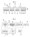
FIG. 5 is a schematic diagram illustrating an electrostatic charge removing unit applied to the electrostatic chuck according to the embodiment of the present invention. - Referring to
FIG. 5 , an electrostaticcharge removing unit 40a according to the embodiment of the present invention includes a dischargingunit 43 and asecond controller 50a. - The discharging
unit 43 generates positive ions and negative ions using corona discharge when a predetermined voltage is applied from thesecond controller 50a. A face of the dischargingunit 43 from which ions are discharged is disposed to face the openings formed in the electrode pad. - The
second controller 50a includes apower supply 52, a switchingunit 54, ahigh voltage generator 56, and a micro-computer 58. Thepower supply 52 supplies an internal power or an external power to thehigh voltage generator 56 and the micro-computer 58. Thepower supply 52 can include a voltage converter converting a first voltage level (for example, 24V) into a second voltage level (for example, 5V). The voltage converter can include a high voltage transistor, an inductor coil, and a Schottky diode or a high voltage transistor, a high voltage transformer, and a Schottky diode. The switchingunit 54 allows or breaks an electrical connection between thepower supply 52 and thehigh voltage generator 56 according to a control by themicro-computer 58. Thehigh voltage generator 56 generates a high DC voltage (for example, 5 kV) by converting a predetermined DC voltage (for example, 24V) supplied from thepower supply 52 and can supply the generated high voltage to the dischargingunit 43. Thehigh voltage generator 56 can be implemented by a high voltage transistor outputting high positive and negative pulses. The micro-computer 58 receives the electric power from thepower supply 52 and controls overall operation of thesecond controller 50a. - Moreover, the electrostatic
charge removing unit 40a may include ablowing unit 60 and asensor 62. The blowingunit 60 forms a flow of fluid (for example, air flow) for compulsive transfer of the ions which are generated from the dischargingunit 43 to the openings of the electrode pad. Thesensor 62 senses a balanced state of the positive ions and negative ions which are generated by the corona discharge of the dischargingunit 43 and transmits an output signal corresponding to the sensed state to themicro-computer 58. -
FIG. 6A is a perspective view illustrating the electrostatic charge removing unit applied to the electrostatic chuck according to the embodiment of the present invention.FIG. 6B is an enlarged plan view illustrating a part of a discharging unit of the electrostatic charge removing unit ofFIG. 6A . - Referring to
FIG. 6A , an electrostaticcharge removing unit 40a according to this embodiment of the present invention includes a dischargingunit 43, asecond controller 50a, a blowingunit 60, and asensor 62. - The discharging
unit 43 includes a minus-shapedbar type housing 44 and a plurality ofunit dischargers 43a. Thehousing 44 supports the plurality ofunit dischargers 43a, and includes wires connecting the respective dischargingunits 43a to thesecond controller 50a and passages communicating therespective unit dischargers 43a with the blowingunit 60. - The plurality of
unit dischargers 43a is approximately aligned with each other by a predetermined distance on a side of thehousing 44. Each of theunit dischargers 43a has a nozzle shape. The side of thehousing 44 on which the plurality ofunit dischargers 43a are disposed can be installed to face the openings of the electrode pad forming a sucking unit of the electrostatic chuck. - Each of the
respective unit dischargers 43a according to the embodiment of the present invention, as illustrated inFIG. 6B , includes aninsulation nozzle body 44a, aground electrode 46, a dischargingelectrode holder 47, and a dischargingelectrode 48. Theinsulation nozzle body 44a is disposed on a side of thehousing 44 and has a hollow part and an open end. Theinsulation nozzle body 44a fixes theunit dischargers 43a to thehousing 44 and electrically insulates thehousing 44 from theground electrode 46. Theground electrode 46 is disposed to cover a majority of inner surface of the hollow part of thenozzle body 44a. The dischargingelectrode holder 47 is fixed to thenozzle body 44a and is disposed at the center of the hollow part of thenozzle body 44a to be spaced apart from theground electrode 46. - The discharging
electrode 48 is coupled with and settled to the dischargingelectrode holder 47, and an end thereof is connected to the high voltage generator of thesecond controller 50a by a wire. The other end of the dischargingelectrode 48 can have a needle shape and can be disposed to face the openings of the electrode pad of the electrostatic chuck. The dischargingelectrode 48 can use a specialized durable electrode wear of which is prevented (for example, an electrode using an X-material). - Moreover, each of the
unit dischargers 43a has a space formed between theground electrode 46 and the dischargingelectrode holder 47. Thisspace 45 is a passage through the fluid is flown by the blowingunit 60. The ions generated from the dischargingelectrode 48 can be introduced into the openings of the electrode pad by the fluid flow discharged to the outside through thespace 45. - The blowing
unit 60 is coupled with a side of thehousing 44 and forms the fluid flow in each of therespective unit dischargers 43a which are arranged in thehousing 44. The blowingunit 60 can be implemented by a blower making a wind using a pressure of a rubber tube and a fan to which an electric motor is mounted. - The
sensor 62 can be coupled with a side of thehousing 44, senses a balanced state of the positive ions and negative ions generated from at least onesingle unit discharger 43a, and transmits an output signal corresponding to the sensed state to thesecond controller 50a. An air ion concentrate gauge can be used as thesensor 62. -
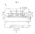
FIG. 7 is a schematic view illustrating an apparatus for manufacturing an OLED according to the present invention. - Referring to
FIG. 7 , theapparatus 100 for manufacturing an OLED according to the embodiment of the present invention includes avacuum chamber 110, anelectrostatic chuck 120, and amechanical unit 140. - The
vacuum chamber 110 includes a chamber providing high vacuum atmosphere under about 104 kPa. Thevacuum chamber 110 includes avacuum pump 112 making the inside of the chamber a vacuum state. Nitrogen gas can be injected into thevacuum chamber 110 in order to prevent impurities from being scattered after a small amount of the impurities is extracted and accumulated around the discharging electrode that is disposed in the dischargingunit 124. - The
electrostatic chuck 120 includes anelectrode pad 122 and afirst controller 130a which form a sucking unit, a dischargingunit 124 and asecond controller 130b which form an electrostatic charge removing unit. Thefirst controller 130a applies a first voltage to chucking electrodes of theelectrode pad 122 and thesecond controller 130b applies a second voltage to dechucking electrodes of the dischargingunit 124. Theelectrostatic chuck 120 draws (or sucks) and supports asubstrate 101 in the face-down method. - The
electrostatic chuck 120 of this embodiment of the present invention can include any one of the electrostatic chucks which are already described with reference toFIGS. 1 to 6B . - When the
first controller 130a applies voltages to the chucking electrodes, a strong electric field is generated between theelectrostatic chuck 120 and thesubstrate 101 and polarization is generated on the surface of thesubstrate 101. In this case, a potential difference and a columbic force are generated between afirst surface 120a of theelectrostatic chuck 120 and thesubstrate 101 so that thesubstrate 101 is drawn to thefirst surface 120a of theelectrostatic chuck 120. The voltages applied to the chucking electrodes can be selected in a range of several hundred volts (V) to several kilovolts (kV). The voltage could be a positive or negative voltage. - Particularly, since a space between the
electrostatic chuck 120 andsubstrate 101 is a vacuum state within thevacuum chamber 110, thesubstrate 101 is completely attached to thefirst surface 120a of theelectrostatic chuck 120. This attached degree, that is, a contact rate can be increased when the insulation plate is made of polyimide and a buffer layer is disposed between the insulation plate and a supporting member in the electrode pad. - When the above-mentioned
electrostatic chuck 120 is used, a glass substrate with a thickness of about 0.7mm and a size of 1,870×2,200mm or 2,200×2,500mm can be stably transferred or fixed. - Meanwhile, the
substrate 101 completely attached to theelectrostatic chuck 120 has a tendency to still stick to thefirst face 120a of theelectrostatic duck 120 even after the high chucking voltage is turned off. Since this tendency affects control of the dechucking of thesubstrate 101 and disturbs smooth processing, and may bring damage of thesubstrate 101 during the dechucking. Therefore, in theapparatus 100 for manufacturing an OLED according to this embodiment of the present invention, a separated electrostatic charge removing unit is disposed in theelectrostatic chuck 120 to control the dechuckcing. - When a predetermined voltage is applied from the
second controller 130b to the dischargingunit 124, positive ions and negative ions are generated by corona discharge of the discharging electrode. The generated ions move to thefirst surface 120a throughopenings 121 of theelectrostatic chuck 120. At this time, when an effective charge removing distance between the discharging electrode and thesubstrate 101 is required, an extended passage of a predetermined length can be added between the dischargingunit 124 and theelectrostatic chuck 120. The extended passage can include a conduit extending theopenings 121 of theelectrostatic chuck 120 toward the dischargingunits 124 by a predetermined length. - According to the above-mentioned
electrostatic chuck 120, the polarization and the potential difference of the surface of thesubstrate 101 are effectively canceled during the dechucking following the chucking of thesubstrate 101 so that the dechucking can be smoothly performed. - The
mechanical unit 140 is disposed in thevacuum chamber 110, supports theelectrostatic chuck 120, and moves theelectrostatic chuck 120 in a desired direction. For example, themechanical unit 140 can include a plurality of pin units coupled with the electrode pad of theelectrostatic chuck 120, an association unit to which the plurality of pin units is fixed, and an elevation unit elevating the association unit. The elevation unit can include an elevation motor having a spiral shaft and a nut housing having an end connected to the spiral shaft and the other end connected to the association unit. Themechanical unit 140 can include a firstmechanical unit 142 supporting and moving theelectrode pad 122 of theelectrostatic chuck 120 and a secondmechanical unit 144 supporting and moving the dischargingunit 124 of theelectrostatic chuck 120. - The
apparatus 100 of an OLED according to this embodiment of the present invention includes a deposition device forming an organic thin film or a conductive layer in red (R), green (G), and blue (B) on thesubstrate 101 in a predetermined pattern. In this case, theapparatus 100 may include anevaporation source 150 evaporating an organic material and metal onto the substrate by evaporating the same and amask 160. - In the
apparatus 100 including theelectrostatic chuck 120 according to this embodiment of the present invention, the evaporation can be performed as follows. That is, after themask 160 is disposed above theevaporation source 150 installed in thevacuum chamber 110 and the substrate 101 a thin film of which is formed is mounted above themask 160 using theelectrostatic chuck 120, a magnetic array (not shown) is driven to make themask 160 be attached close to thesubstrate 101. Then, theevaporation source 150 is driven. An organic material installed in theevaporation source 150 is evaporated and passes through a slit of themask 160 to be deposited on a side of thesubstrate 101 in a predetermined pattern. - When the
electrostatic chuck 120 is used during the evaporation process, a large sized substrate can be chucked in the face-down method with a high flatness and thesubstrate 101 can be safely dechcucked after the evaporation. Therefore, a potential handling error of the large sized substrate is prevented and thesubstrate 101 is prevented from being damaged. Tact time (time for outputting a next substrate after outputting one substrate) can be reduced and yield and quality of complete (final) products can be increased. - While the present invention has been described in connection with certain exemplary embodiments, it is to be understood that the invention is not limited to the disclosed embodiments, but, on the contrary, is intended to cover various modifications and equivalent arrangements included within the scope of the appended claims, and equivalents thereof.
Claims (15)
- An electrostatic chuck comprising:an insulating plate (21) having at least one opening (30a, 30b, 30c) penetrating the insulating plate (21);a pair of electrodes (23a, 23b);a first controller (130a) adapted for applying a voltage to the pair of electrodes (23a, 23b); andan electrostatic charge removing unit (40, 40a) adapted for emitting ions into the at least one opening (30a, 30b, 30c) of the insulating plate (21) to remove electrostatic charges.
- The electrostatic chuck as claimed in claim 1, wherein the pair of electrodes (23a, 23b) is mounted on the insulating plate (21) and/or wherein the electrostatic charge removing unit (40, 40a) comprises at least one discharging unit (43, 42a, 42b, 42c) which is arranged such to cover a respective opening (30a, 30b, 30c) of the insulating plate (21).
- The electrostatic chuck according to any one of the preceding claims, wherein the at least one opening (30a, 30b, 30c) has a stripe shape extending in a direction parallel to an edge of the insulating plate (21).
- The electrostatic chuck according to any one of the preceding claims, wherein the pair of electrodes (23a, 23b) is arranged in a laminated structure, wherein at least a part of the insulating plate (21) is disposed between the pair of electrodes (23a, 23b).
- The electrostatic chuck according to any one of claims 1-3, wherein one electrode (23a) of the pair of the electrodes and the other electrode (23b) of the pair of the electrodes are arranged on the same plane which extends parallel to a surface of the insulating plate (21) on which the at least one opening (30a, 30b, 30c) is formed.
- The electrostatic chuck according to any one of the preceding claims, wherein the insulating plate (21) is made of a material including resin or ceramic.
- The electrostatic chuck according to any one of the preceding claims, further comprising a supporting member (32) adapted for supporting the insulating plate (21).
- The electrostatic chuck as claimed in claim 7, further comprising a buffer layer (34) formed between the insulating plate (21) and the supporting member (32).
- The electrostatic chuck according to any one of the preceding claims, wherein the electrostatic charge removing unit (40, 40a) comprises:at least one discharging unit (43, 42a, 42b, 42c) adapted for generating ions by corona discharge; anda second controller (50a, 130b) adapted for applying a voltage to the discharging unit.
- The electrostatic chuck as claimed in claim 8, wherein the least one discharging unit (43, 42a, 42b, 42c) is arranged to cover the at least one opening (30a, 30b, 30c).
- The electrostatic chuck according to any one of the claims 9 and 10, wherein the electrostatic charge removing unit (40, 40a) further comprises a blowing unit (60) adapted for compulsively blowing ions generated in the discharging unit (43, 42a, 42b, 42c) to the at least one opening (30a, 30b, 30c).
- The electrostatic chuck according to any one of the claims 9 to 11, wherein the electrostatic charge removing unit (40, 40a) further comprises a sensor (62) adapted for sensing a degree of balance between positive ions and negative ions which are generated in the discharging unit (43, 42a, 42b, 42c) and adapted for transmitting an output signal with respect to the sensed balance to the second controller (50a, 130b).
- An apparatus for manufacturing an organic light emitting diode comprising:a vacuum chamber (110);an electrostatic chuck according to any one of preceding claims,the electrostatic chuck being adapted for supporting a substrate (101) inside the vacuum chamber (110); and
a mechanical unit (140) coupled with the vacuum chamber (110) and adapted for supporting and moving the electrostatic chuck - The apparatus according to claim 13, wherein the mechanical unit (140) comprises:a first mechanical unit supporting the insulating plate of the electrostatic chuck; anda second mechanical unit supporting the electrostatic charge removing unit of the electrostatic chuck.
- The apparatus according to any one of claims 13 and 14, further comprising an evaporation source evaporating an organic material or metal to a surface of the substrate.
Applications Claiming Priority (1)
| Application Number | Priority Date | Filing Date | Title |
|---|---|---|---|
| KR1020090006200A KR101001454B1 (en) | 2009-01-23 | 2009-01-23 | Electrostatic chuck and apparatus for manufacturing organic electroluminescent device having same |
Publications (2)
| Publication Number | Publication Date |
|---|---|
| EP2211379A1 true EP2211379A1 (en) | 2010-07-28 |
| EP2211379B1 EP2211379B1 (en) | 2013-10-16 |
Family
ID=41563262
Family Applications (1)
| Application Number | Title | Priority Date | Filing Date |
|---|---|---|---|
| EP09175414.3A Active EP2211379B1 (en) | 2009-01-23 | 2009-11-09 | Electrostatic chuck and device of manufacturing organic light emitting diode having the same |
Country Status (4)
| Country | Link |
|---|---|
| US (1) | US8325457B2 (en) |
| EP (1) | EP2211379B1 (en) |
| JP (1) | JP5222806B2 (en) |
| KR (1) | KR101001454B1 (en) |
Cited By (5)
| Publication number | Priority date | Publication date | Assignee | Title |
|---|---|---|---|---|
| CN103456669A (en) * | 2012-06-01 | 2013-12-18 | 英飞凌科技股份有限公司 | Thin substrate electrostatic chuck system and method |
| CN104054168A (en) * | 2011-11-18 | 2014-09-17 | 勒克斯维科技公司 | Method of transferring micro device |
| US9831383B2 (en) | 2011-11-18 | 2017-11-28 | Apple Inc. | LED array |
| US10121864B2 (en) | 2011-11-18 | 2018-11-06 | Apple Inc. | Micro device transfer head heater assembly and method of transferring a micro device |
| US10297712B2 (en) | 2011-11-18 | 2019-05-21 | Apple Inc. | Micro LED display |
Families Citing this family (84)
| Publication number | Priority date | Publication date | Assignee | Title |
|---|---|---|---|---|
| US8518204B2 (en) | 2011-11-18 | 2013-08-27 | LuxVue Technology Corporation | Method of fabricating and transferring a micro device and an array of micro devices utilizing an intermediate electrically conductive bonding layer |
| JP5994089B2 (en) * | 2011-12-29 | 2016-09-21 | 株式会社ブイ・テクノロジー | Vapor deposition equipment |
| US9773750B2 (en) | 2012-02-09 | 2017-09-26 | Apple Inc. | Method of transferring and bonding an array of micro devices |
| US9548332B2 (en) | 2012-04-27 | 2017-01-17 | Apple Inc. | Method of forming a micro LED device with self-aligned metallization stack |
| US9105492B2 (en) | 2012-05-08 | 2015-08-11 | LuxVue Technology Corporation | Compliant micro device transfer head |
| US8415771B1 (en) | 2012-05-25 | 2013-04-09 | LuxVue Technology Corporation | Micro device transfer head with silicon electrode |
| US9034754B2 (en) | 2012-05-25 | 2015-05-19 | LuxVue Technology Corporation | Method of forming a micro device transfer head with silicon electrode |
| US8415767B1 (en) | 2012-07-06 | 2013-04-09 | LuxVue Technology Corporation | Compliant bipolar micro device transfer head with silicon electrodes |
| US8383506B1 (en) | 2012-07-06 | 2013-02-26 | LuxVue Technology Corporation | Method of forming a compliant monopolar micro device transfer head with silicon electrode |
| US8415768B1 (en) | 2012-07-06 | 2013-04-09 | LuxVue Technology Corporation | Compliant monopolar micro device transfer head with silicon electrode |
| US8569115B1 (en) | 2012-07-06 | 2013-10-29 | LuxVue Technology Corporation | Method of forming a compliant bipolar micro device transfer head with silicon electrodes |
| US8933433B2 (en) | 2012-07-30 | 2015-01-13 | LuxVue Technology Corporation | Method and structure for receiving a micro device |
| US8791530B2 (en) | 2012-09-06 | 2014-07-29 | LuxVue Technology Corporation | Compliant micro device transfer head with integrated electrode leads |
| US9162880B2 (en) | 2012-09-07 | 2015-10-20 | LuxVue Technology Corporation | Mass transfer tool |
| US8941215B2 (en) | 2012-09-24 | 2015-01-27 | LuxVue Technology Corporation | Micro device stabilization post |
| US8835940B2 (en) | 2012-09-24 | 2014-09-16 | LuxVue Technology Corporation | Micro device stabilization post |
| US9558721B2 (en) | 2012-10-15 | 2017-01-31 | Apple Inc. | Content-based adaptive refresh schemes for low-power displays |
| US9029880B2 (en) | 2012-12-10 | 2015-05-12 | LuxVue Technology Corporation | Active matrix display panel with ground tie lines |
| US9236815B2 (en) | 2012-12-10 | 2016-01-12 | LuxVue Technology Corporation | Compliant micro device transfer head array with metal electrodes |
| US9178123B2 (en) | 2012-12-10 | 2015-11-03 | LuxVue Technology Corporation | Light emitting device reflective bank structure |
| US9255001B2 (en) | 2012-12-10 | 2016-02-09 | LuxVue Technology Corporation | Micro device transfer head array with metal electrodes |
| US9159700B2 (en) | 2012-12-10 | 2015-10-13 | LuxVue Technology Corporation | Active matrix emissive micro LED display |
| US9105714B2 (en) | 2012-12-11 | 2015-08-11 | LuxVue Technology Corporation | Stabilization structure including sacrificial release layer and staging bollards |
| US9166114B2 (en) | 2012-12-11 | 2015-10-20 | LuxVue Technology Corporation | Stabilization structure including sacrificial release layer and staging cavity |
| US9314930B2 (en) | 2012-12-14 | 2016-04-19 | LuxVue Technology Corporation | Micro pick up array with integrated pivot mount |
| US9391042B2 (en) | 2012-12-14 | 2016-07-12 | Apple Inc. | Micro device transfer system with pivot mount |
| US9153171B2 (en) | 2012-12-17 | 2015-10-06 | LuxVue Technology Corporation | Smart pixel lighting and display microcontroller |
| US9308649B2 (en) | 2013-02-25 | 2016-04-12 | LuxVue Techonology Corporation | Mass transfer tool manipulator assembly |
| US9095980B2 (en) * | 2013-02-25 | 2015-08-04 | LuxVue Technology Corporation | Micro pick up array mount with integrated displacement sensor |
| US8791474B1 (en) | 2013-03-15 | 2014-07-29 | LuxVue Technology Corporation | Light emitting diode display with redundancy scheme |
| US9252375B2 (en) | 2013-03-15 | 2016-02-02 | LuxVue Technology Corporation | Method of fabricating a light emitting diode display with integrated defect detection test |
| KR101319785B1 (en) | 2013-03-18 | 2013-10-18 | 주식회사 야스 | Apparatus for substrate transportation using electrostatic floating |
| US9217541B2 (en) | 2013-05-14 | 2015-12-22 | LuxVue Technology Corporation | Stabilization structure including shear release posts |
| US9484504B2 (en) | 2013-05-14 | 2016-11-01 | Apple Inc. | Micro LED with wavelength conversion layer |
| US9136161B2 (en) | 2013-06-04 | 2015-09-15 | LuxVue Technology Corporation | Micro pick up array with compliant contact |
| EP3008553B1 (en) | 2013-06-12 | 2023-06-07 | Rohinni, Inc. | Keyboard backlighting with deposited light-generating sources |
| US8987765B2 (en) | 2013-06-17 | 2015-03-24 | LuxVue Technology Corporation | Reflective bank structure and method for integrating a light emitting device |
| US9111464B2 (en) | 2013-06-18 | 2015-08-18 | LuxVue Technology Corporation | LED display with wavelength conversion layer |
| US8928021B1 (en) | 2013-06-18 | 2015-01-06 | LuxVue Technology Corporation | LED light pipe |
| US9035279B2 (en) | 2013-07-08 | 2015-05-19 | LuxVue Technology Corporation | Micro device with stabilization post |
| WO2015013142A1 (en) | 2013-07-22 | 2015-01-29 | Applied Materials, Inc. | An electrostatic chuck for high temperature process applications |
| US9296111B2 (en) | 2013-07-22 | 2016-03-29 | LuxVue Technology Corporation | Micro pick up array alignment encoder |
| US9087764B2 (en) | 2013-07-26 | 2015-07-21 | LuxVue Technology Corporation | Adhesive wafer bonding with controlled thickness variation |
| CN105359265B (en) | 2013-08-05 | 2018-12-14 | 应用材料公司 | removable electrostatic chuck in situ |
| CN105408992B (en) | 2013-08-05 | 2019-01-29 | 应用材料公司 | Electrostatic Carrier for Thin Substrate Handling |
| KR101905158B1 (en) | 2013-08-06 | 2018-10-08 | 어플라이드 머티어리얼스, 인코포레이티드 | Locally heated multi-zone substrate support |
| US9153548B2 (en) | 2013-09-16 | 2015-10-06 | Lux Vue Technology Corporation | Adhesive wafer bonding with sacrificial spacers for controlled thickness variation |
| CN105579612B (en) | 2013-09-20 | 2019-06-14 | 应用材料公司 | Substrate carrier with integrated electrostatic chuck |
| US9460950B2 (en) | 2013-12-06 | 2016-10-04 | Applied Materials, Inc. | Wafer carrier for smaller wafers and wafer pieces |
| US9367094B2 (en) | 2013-12-17 | 2016-06-14 | Apple Inc. | Display module and system applications |
| US9768345B2 (en) | 2013-12-20 | 2017-09-19 | Apple Inc. | LED with current injection confinement trench |
| US9450147B2 (en) | 2013-12-27 | 2016-09-20 | Apple Inc. | LED with internally confined current injection area |
| US9583466B2 (en) | 2013-12-27 | 2017-02-28 | Apple Inc. | Etch removal of current distribution layer for LED current confinement |
| US9542638B2 (en) | 2014-02-18 | 2017-01-10 | Apple Inc. | RFID tag and micro chip integration design |
| US9583533B2 (en) | 2014-03-13 | 2017-02-28 | Apple Inc. | LED device with embedded nanowire LEDs |
| US9522468B2 (en) | 2014-05-08 | 2016-12-20 | Apple Inc. | Mass transfer tool manipulator assembly with remote center of compliance |
| US10153191B2 (en) | 2014-05-09 | 2018-12-11 | Applied Materials, Inc. | Substrate carrier system and method for using the same |
| US10096509B2 (en) | 2014-05-09 | 2018-10-09 | Applied Materials, Inc. | Substrate carrier system with protective covering |
| US9318475B2 (en) | 2014-05-15 | 2016-04-19 | LuxVue Technology Corporation | Flexible display and method of formation with sacrificial release layer |
| US9959961B2 (en) | 2014-06-02 | 2018-05-01 | Applied Materials, Inc. | Permanent magnetic chuck for OLED mask chucking |
| US9741286B2 (en) | 2014-06-03 | 2017-08-22 | Apple Inc. | Interactive display panel with emitting and sensing diodes |
| US9624100B2 (en) | 2014-06-12 | 2017-04-18 | Apple Inc. | Micro pick up array pivot mount with integrated strain sensing elements |
| US9425151B2 (en) | 2014-06-17 | 2016-08-23 | Apple Inc. | Compliant electrostatic transfer head with spring support layer |
| US9570002B2 (en) | 2014-06-17 | 2017-02-14 | Apple Inc. | Interactive display panel with IR diodes |
| US9705432B2 (en) | 2014-09-30 | 2017-07-11 | Apple Inc. | Micro pick up array pivot mount design for strain amplification |
| US9828244B2 (en) | 2014-09-30 | 2017-11-28 | Apple Inc. | Compliant electrostatic transfer head with defined cavity |
| KR102235605B1 (en) * | 2014-10-08 | 2021-04-06 | 삼성디스플레이 주식회사 | Deposition apparatus and deposition method using the same |
| KR102398067B1 (en) | 2014-11-05 | 2022-05-13 | 삼성디스플레이 주식회사 | Electrostatic chuck |
| US9478583B2 (en) | 2014-12-08 | 2016-10-25 | Apple Inc. | Wearable display having an array of LEDs on a conformable silicon substrate |
| CN107636820B (en) | 2015-06-04 | 2022-01-07 | 应用材料公司 | Transparent electrostatic carrier |
| KR20170039781A (en) | 2015-10-01 | 2017-04-12 | 삼성디스플레이 주식회사 | Electrostatic chuck and substrate processing apparatus including the same |
| JP6056025B2 (en) * | 2015-11-26 | 2017-01-11 | 株式会社昭和真空 | Deposition equipment |
| US10629393B2 (en) | 2016-01-15 | 2020-04-21 | Rohinni, LLC | Apparatus and method of backlighting through a cover on the apparatus |
| JP6238097B1 (en) * | 2016-07-20 | 2017-11-29 | Toto株式会社 | Electrostatic chuck |
| CN106626713B (en) * | 2016-11-17 | 2018-06-01 | 无锡市伟丰印刷机械厂 | A kind of static removal equipment for copper-clad plate production |
| US20200083280A1 (en) * | 2018-09-11 | 2020-03-12 | Prilit Optronics, Inc. | Top emission microled display and bottom emission microled display and a method of forming the same |
| CN112242277B (en) * | 2019-07-16 | 2022-03-18 | 清华大学 | Field Emission Neutralizer |
| CN112242276B (en) * | 2019-07-16 | 2022-03-22 | 清华大学 | Field emission neutralizer |
| KR102764544B1 (en) * | 2019-09-18 | 2025-02-10 | 주식회사 선익시스템 | Substrate inducing holder |
| KR20220082132A (en) | 2020-12-09 | 2022-06-17 | 삼성디스플레이 주식회사 | Deposition apparatus and display panel manufacturing apparatus including the same |
| US11417557B2 (en) | 2020-12-15 | 2022-08-16 | Entegris, Inc. | Spiraling polyphase electrodes for electrostatic chuck |
| KR102878850B1 (en) * | 2021-04-14 | 2025-11-03 | 삼성디스플레이 주식회사 | Substarte transfer apparatus and method for preventing water inflow thereof |
| KR20230120224A (en) * | 2022-02-08 | 2023-08-17 | 삼성디스플레이 주식회사 | Apparatus for manufacturing display appratus and method for manufacturing display apparatus |
| CN117127160B (en) * | 2023-08-30 | 2024-05-28 | 苏州佑伦真空设备科技有限公司 | Large-area film-plating substrate device |
Citations (8)
| Publication number | Priority date | Publication date | Assignee | Title |
|---|---|---|---|---|
| JPH06188305A (en) * | 1992-12-17 | 1994-07-08 | Tokyo Electron Ltd | Apparatus and method for separation of body to be attracted as well as plasma processing apparatus |
| JPH06275546A (en) * | 1993-03-24 | 1994-09-30 | Tokyo Electron Ltd | Plasma treating device |
| US5382311A (en) * | 1992-12-17 | 1995-01-17 | Tokyo Electron Limited | Stage having electrostatic chuck and plasma processing apparatus using same |
| US5474614A (en) | 1994-06-10 | 1995-12-12 | Texas Instruments Incorporated | Method and apparatus for releasing a semiconductor wafer from an electrostatic clamp |
| US20070000441A1 (en) * | 2005-07-01 | 2007-01-04 | Applied Materials, Inc. | Scalable uniform thermal plate |
| US20070223173A1 (en) * | 2004-03-19 | 2007-09-27 | Hiroshi Fujisawa | Bipolar Electrostatic Chuck |
| JP2007311462A (en) * | 2006-05-17 | 2007-11-29 | Disco Abrasive Syst Ltd | Electrostatic chuck table mechanism |
| JP2008294257A (en) * | 2007-05-25 | 2008-12-04 | Seiko Epson Corp | Semiconductor substrate detachment method and electrostatic chuck device |
Family Cites Families (19)
| Publication number | Priority date | Publication date | Assignee | Title |
|---|---|---|---|---|
| JPH06267899A (en) * | 1993-03-16 | 1994-09-22 | Nippon Steel Corp | Etching device |
| JP3311812B2 (en) * | 1993-04-09 | 2002-08-05 | 東京エレクトロン株式会社 | Electrostatic chuck |
| KR100278180B1 (en) | 1998-11-05 | 2001-02-01 | 고석태 | A method of forming an insulating film provided in an electrostatic chuck assembly and an electrostatic chuck assembly of a semiconductor device etching facility and a method of manufacturing the electrostatic chuck assembly |
| KR20010091088A (en) | 2000-03-13 | 2001-10-23 | 윤종용 | Electrostatic chuck(ESC) |
| JP3382230B2 (en) * | 2000-11-27 | 2003-03-04 | 松下電工株式会社 | Ion generator and hair brush with ion generator |
| JP4493863B2 (en) * | 2001-01-25 | 2010-06-30 | 東京エレクトロン株式会社 | Plasma processing apparatus, cleaning method thereof, and electrostatic chuck static elimination method |
| JP2002313902A (en) * | 2001-04-18 | 2002-10-25 | Canon Inc | Electrostatic chuck and method for releasing substrate from electrostatic chuck |
| JP2003017255A (en) * | 2001-06-29 | 2003-01-17 | Sanyo Electric Co Ltd | Method of manufacturing electroluminescence display device |
| JP2003309156A (en) * | 2002-04-16 | 2003-10-31 | Ulvac Japan Ltd | Substrate discharging method, substrate discharging device and vacuum treatment device |
| JP2004022979A (en) * | 2002-06-19 | 2004-01-22 | Shibaura Mechatronics Corp | Suction stage and substrate bonding apparatus using the same |
| JP2004183044A (en) * | 2002-12-03 | 2004-07-02 | Seiko Epson Corp | Mask evaporation method and apparatus, mask and mask manufacturing method, display panel manufacturing apparatus, display panel, and electronic equipment |
| JP4363903B2 (en) * | 2003-06-05 | 2009-11-11 | 株式会社キーエンス | Static eliminator |
| JP4031419B2 (en) | 2003-09-19 | 2008-01-09 | 日本碍子株式会社 | Electrostatic chuck and manufacturing method thereof |
| KR100694530B1 (en) | 2004-12-17 | 2007-03-13 | 주식회사 에이디피엔지니어링 | Board Bonding Device |
| JP4639311B2 (en) * | 2005-02-21 | 2011-02-23 | 独立行政法人産業技術総合研究所 | Ion generator and static eliminator |
| KR100745153B1 (en) | 2005-12-22 | 2007-08-01 | 주식회사 래디언테크 | Plasma treatment apparatus and method |
| KR20080058144A (en) | 2006-12-21 | 2008-06-25 | 엘지디스플레이 주식회사 | Bonding method of electrostatic chuck and flat panel display device using same |
| JP4811731B2 (en) * | 2007-02-14 | 2011-11-09 | Smc株式会社 | Ionizer |
| JP4976915B2 (en) * | 2007-05-08 | 2012-07-18 | 新光電気工業株式会社 | Electrostatic chuck and method of manufacturing electrostatic chuck |
-
2009
- 2009-01-23 KR KR1020090006200A patent/KR101001454B1/en active Active
- 2009-07-14 JP JP2009165792A patent/JP5222806B2/en not_active Expired - Fee Related
- 2009-09-28 US US12/585,895 patent/US8325457B2/en active Active
- 2009-11-09 EP EP09175414.3A patent/EP2211379B1/en active Active
Patent Citations (8)
| Publication number | Priority date | Publication date | Assignee | Title |
|---|---|---|---|---|
| JPH06188305A (en) * | 1992-12-17 | 1994-07-08 | Tokyo Electron Ltd | Apparatus and method for separation of body to be attracted as well as plasma processing apparatus |
| US5382311A (en) * | 1992-12-17 | 1995-01-17 | Tokyo Electron Limited | Stage having electrostatic chuck and plasma processing apparatus using same |
| JPH06275546A (en) * | 1993-03-24 | 1994-09-30 | Tokyo Electron Ltd | Plasma treating device |
| US5474614A (en) | 1994-06-10 | 1995-12-12 | Texas Instruments Incorporated | Method and apparatus for releasing a semiconductor wafer from an electrostatic clamp |
| US20070223173A1 (en) * | 2004-03-19 | 2007-09-27 | Hiroshi Fujisawa | Bipolar Electrostatic Chuck |
| US20070000441A1 (en) * | 2005-07-01 | 2007-01-04 | Applied Materials, Inc. | Scalable uniform thermal plate |
| JP2007311462A (en) * | 2006-05-17 | 2007-11-29 | Disco Abrasive Syst Ltd | Electrostatic chuck table mechanism |
| JP2008294257A (en) * | 2007-05-25 | 2008-12-04 | Seiko Epson Corp | Semiconductor substrate detachment method and electrostatic chuck device |
Cited By (12)
| Publication number | Priority date | Publication date | Assignee | Title |
|---|---|---|---|---|
| CN104054168A (en) * | 2011-11-18 | 2014-09-17 | 勒克斯维科技公司 | Method of transferring micro device |
| US9620478B2 (en) | 2011-11-18 | 2017-04-11 | Apple Inc. | Method of fabricating a micro device transfer head |
| CN104054168B (en) * | 2011-11-18 | 2017-06-16 | 苹果公司 | The method for transmitting micro element |
| US9831383B2 (en) | 2011-11-18 | 2017-11-28 | Apple Inc. | LED array |
| US10121864B2 (en) | 2011-11-18 | 2018-11-06 | Apple Inc. | Micro device transfer head heater assembly and method of transferring a micro device |
| US10297712B2 (en) | 2011-11-18 | 2019-05-21 | Apple Inc. | Micro LED display |
| US10607961B2 (en) | 2011-11-18 | 2020-03-31 | Apple Inc. | Micro device transfer head heater assembly and method of transferring a micro device |
| US11552046B2 (en) | 2011-11-18 | 2023-01-10 | Apple Inc. | Micro device transfer head assembly |
| US12243955B2 (en) | 2011-11-18 | 2025-03-04 | Apple Inc. | Display and micro device array for transfer to a display substrate |
| CN103456669A (en) * | 2012-06-01 | 2013-12-18 | 英飞凌科技股份有限公司 | Thin substrate electrostatic chuck system and method |
| US9601363B2 (en) | 2012-06-01 | 2017-03-21 | Infineon Technologies Ag | Thin substrate electrostatic chuck system and method |
| CN103456669B (en) * | 2012-06-01 | 2017-04-12 | 英飞凌科技股份有限公司 | thin substrate electrostatic chuck system and method |
Also Published As
| Publication number | Publication date |
|---|---|
| KR20100086790A (en) | 2010-08-02 |
| EP2211379B1 (en) | 2013-10-16 |
| US20100188794A1 (en) | 2010-07-29 |
| US8325457B2 (en) | 2012-12-04 |
| JP5222806B2 (en) | 2013-06-26 |
| JP2010170982A (en) | 2010-08-05 |
| KR101001454B1 (en) | 2010-12-14 |
Similar Documents
| Publication | Publication Date | Title |
|---|---|---|
| EP2211379B1 (en) | Electrostatic chuck and device of manufacturing organic light emitting diode having the same | |
| CN101261952B (en) | Substrate carrying bench and substrate treatment device | |
| TWI327336B (en) | Arrangement for processing a substrate | |
| US9463543B2 (en) | Electromagnetic chuck for OLED mask chucking | |
| US20130240870A1 (en) | Vapor deposition device, vapor deposition method and organic el display device | |
| JP2001525616A (en) | Electrostatic chuck that can release the substrate quickly | |
| US20220255050A1 (en) | Organic layer deposition apparatus and method of manufacturing organic light-emitting display apparatus using the same | |
| JP2004335492A (en) | Coater of organic electronic material and process for producing organic electronic element using it | |
| US8411408B2 (en) | Electrostatic chuck | |
| CN110578118A (en) | Electrostatic chuck system, film forming device, adsorption method, film forming method, and manufacturing method of electronic equipment | |
| JPS63194345A (en) | Electrostatic chuck | |
| US9614155B2 (en) | Vapor deposition apparatus, vapor deposition method, and method for producing organic electroluminescent element | |
| KR20180053143A (en) | The Substrate Holding Apparatus And Substrate Processing Apparatus | |
| US9543151B2 (en) | Ionizer and substrate transfer system having the same, and method of manufacturing a semiconductor device using the same | |
| CN110783248A (en) | Electrostatic chuck system, film forming device, adsorption and film forming method, and manufacturing method of electronic device | |
| KR102496166B1 (en) | Substrate Processing Apparatus having Electrostatic chuck | |
| JP2001353454A (en) | Film forming method, method for manufacturing organic EL element, and film forming apparatus | |
| CN112824558B (en) | Film forming apparatus, film forming method using film forming apparatus, and method for manufacturing electronic device | |
| KR100601558B1 (en) | High frequency antenna and inductively coupled plasma chemical vapor deposition apparatus using the same | |
| US10147633B2 (en) | Transfer apparatus and plasma processing system | |
| KR102629497B1 (en) | The Substrate Holding Apparatus And The Operation Method Of The Same | |
| CN120569512A (en) | Film forming apparatus | |
| KR20250177195A (en) | Deposition apparatus for wafer | |
| KR20080081689A (en) | Electrostatic chuck and substrate plasma processing apparatus using the same | |
| CN119968701A (en) | Film forming device, detection device and control method of film forming device |
Legal Events
| Date | Code | Title | Description |
|---|---|---|---|
| PUAI | Public reference made under article 153(3) epc to a published international application that has entered the european phase |
Free format text: ORIGINAL CODE: 0009012 |
|
| 17P | Request for examination filed |
Effective date: 20091109 |
|
| AK | Designated contracting states |
Kind code of ref document: A1 Designated state(s): AT BE BG CH CY CZ DE DK EE ES FI FR GB GR HR HU IE IS IT LI LT LU LV MC MK MT NL NO PL PT RO SE SI SK SM TR |
|
| AX | Request for extension of the european patent |
Extension state: AL BA RS |
|
| 17Q | First examination report despatched |
Effective date: 20110624 |
|
| RAP1 | Party data changed (applicant data changed or rights of an application transferred) |
Owner name: SAMSUNG DISPLAY CO., LTD. |
|
| GRAP | Despatch of communication of intention to grant a patent |
Free format text: ORIGINAL CODE: EPIDOSNIGR1 |
|
| INTG | Intention to grant announced |
Effective date: 20130531 |
|
| GRAS | Grant fee paid |
Free format text: ORIGINAL CODE: EPIDOSNIGR3 |
|
| GRAA | (expected) grant |
Free format text: ORIGINAL CODE: 0009210 |
|
| AK | Designated contracting states |
Kind code of ref document: B1 Designated state(s): AT BE BG CH CY CZ DE DK EE ES FI FR GB GR HR HU IE IS IT LI LT LU LV MC MK MT NL NO PL PT RO SE SI SK SM TR |
|
| REG | Reference to a national code |
Ref country code: GB Ref legal event code: FG4D |
|
| REG | Reference to a national code |
Ref country code: CH Ref legal event code: EP |
|
| REG | Reference to a national code |
Ref country code: IE Ref legal event code: FG4D |
|
| REG | Reference to a national code |
Ref country code: AT Ref legal event code: REF Ref document number: 636861 Country of ref document: AT Kind code of ref document: T Effective date: 20131115 |
|
| REG | Reference to a national code |
Ref country code: DE Ref legal event code: R096 Ref document number: 602009019445 Country of ref document: DE Effective date: 20131212 |
|
| REG | Reference to a national code |
Ref country code: NL Ref legal event code: VDEP Effective date: 20131016 |
|
| REG | Reference to a national code |
Ref country code: AT Ref legal event code: MK05 Ref document number: 636861 Country of ref document: AT Kind code of ref document: T Effective date: 20131016 |
|
| REG | Reference to a national code |
Ref country code: LT Ref legal event code: MG4D |
|
| PG25 | Lapsed in a contracting state [announced via postgrant information from national office to epo] |
Ref country code: BE Free format text: LAPSE BECAUSE OF FAILURE TO SUBMIT A TRANSLATION OF THE DESCRIPTION OR TO PAY THE FEE WITHIN THE PRESCRIBED TIME-LIMIT Effective date: 20131016 Ref country code: IS Free format text: LAPSE BECAUSE OF FAILURE TO SUBMIT A TRANSLATION OF THE DESCRIPTION OR TO PAY THE FEE WITHIN THE PRESCRIBED TIME-LIMIT Effective date: 20140216 Ref country code: NO Free format text: LAPSE BECAUSE OF FAILURE TO SUBMIT A TRANSLATION OF THE DESCRIPTION OR TO PAY THE FEE WITHIN THE PRESCRIBED TIME-LIMIT Effective date: 20140116 Ref country code: FI Free format text: LAPSE BECAUSE OF FAILURE TO SUBMIT A TRANSLATION OF THE DESCRIPTION OR TO PAY THE FEE WITHIN THE PRESCRIBED TIME-LIMIT Effective date: 20131016 Ref country code: LT Free format text: LAPSE BECAUSE OF FAILURE TO SUBMIT A TRANSLATION OF THE DESCRIPTION OR TO PAY THE FEE WITHIN THE PRESCRIBED TIME-LIMIT Effective date: 20131016 Ref country code: NL Free format text: LAPSE BECAUSE OF FAILURE TO SUBMIT A TRANSLATION OF THE DESCRIPTION OR TO PAY THE FEE WITHIN THE PRESCRIBED TIME-LIMIT Effective date: 20131016 Ref country code: SE Free format text: LAPSE BECAUSE OF FAILURE TO SUBMIT A TRANSLATION OF THE DESCRIPTION OR TO PAY THE FEE WITHIN THE PRESCRIBED TIME-LIMIT Effective date: 20131016 Ref country code: HR Free format text: LAPSE BECAUSE OF FAILURE TO SUBMIT A TRANSLATION OF THE DESCRIPTION OR TO PAY THE FEE WITHIN THE PRESCRIBED TIME-LIMIT Effective date: 20131016 |
|
| PG25 | Lapsed in a contracting state [announced via postgrant information from national office to epo] |
Ref country code: ES Free format text: LAPSE BECAUSE OF FAILURE TO SUBMIT A TRANSLATION OF THE DESCRIPTION OR TO PAY THE FEE WITHIN THE PRESCRIBED TIME-LIMIT Effective date: 20131016 Ref country code: AT Free format text: LAPSE BECAUSE OF FAILURE TO SUBMIT A TRANSLATION OF THE DESCRIPTION OR TO PAY THE FEE WITHIN THE PRESCRIBED TIME-LIMIT Effective date: 20131016 Ref country code: CY Free format text: LAPSE BECAUSE OF FAILURE TO SUBMIT A TRANSLATION OF THE DESCRIPTION OR TO PAY THE FEE WITHIN THE PRESCRIBED TIME-LIMIT Effective date: 20131016 Ref country code: LV Free format text: LAPSE BECAUSE OF FAILURE TO SUBMIT A TRANSLATION OF THE DESCRIPTION OR TO PAY THE FEE WITHIN THE PRESCRIBED TIME-LIMIT Effective date: 20131016 |
|
| PG25 | Lapsed in a contracting state [announced via postgrant information from national office to epo] |
Ref country code: PT Free format text: LAPSE BECAUSE OF FAILURE TO SUBMIT A TRANSLATION OF THE DESCRIPTION OR TO PAY THE FEE WITHIN THE PRESCRIBED TIME-LIMIT Effective date: 20140217 |
|
| REG | Reference to a national code |
Ref country code: CH Ref legal event code: PL |
|
| REG | Reference to a national code |
Ref country code: DE Ref legal event code: R097 Ref document number: 602009019445 Country of ref document: DE |
|
| PG25 | Lapsed in a contracting state [announced via postgrant information from national office to epo] |
Ref country code: MC Free format text: LAPSE BECAUSE OF FAILURE TO SUBMIT A TRANSLATION OF THE DESCRIPTION OR TO PAY THE FEE WITHIN THE PRESCRIBED TIME-LIMIT Effective date: 20131016 Ref country code: EE Free format text: LAPSE BECAUSE OF FAILURE TO SUBMIT A TRANSLATION OF THE DESCRIPTION OR TO PAY THE FEE WITHIN THE PRESCRIBED TIME-LIMIT Effective date: 20131016 Ref country code: CH Free format text: LAPSE BECAUSE OF NON-PAYMENT OF DUE FEES Effective date: 20131130 Ref country code: LI Free format text: LAPSE BECAUSE OF NON-PAYMENT OF DUE FEES Effective date: 20131130 |
|
| PLBE | No opposition filed within time limit |
Free format text: ORIGINAL CODE: 0009261 |
|
| STAA | Information on the status of an ep patent application or granted ep patent |
Free format text: STATUS: NO OPPOSITION FILED WITHIN TIME LIMIT |
|
| REG | Reference to a national code |
Ref country code: IE Ref legal event code: MM4A |
|
| PG25 | Lapsed in a contracting state [announced via postgrant information from national office to epo] |
Ref country code: SK Free format text: LAPSE BECAUSE OF FAILURE TO SUBMIT A TRANSLATION OF THE DESCRIPTION OR TO PAY THE FEE WITHIN THE PRESCRIBED TIME-LIMIT Effective date: 20131016 Ref country code: RO Free format text: LAPSE BECAUSE OF FAILURE TO SUBMIT A TRANSLATION OF THE DESCRIPTION OR TO PAY THE FEE WITHIN THE PRESCRIBED TIME-LIMIT Effective date: 20131016 Ref country code: IT Free format text: LAPSE BECAUSE OF FAILURE TO SUBMIT A TRANSLATION OF THE DESCRIPTION OR TO PAY THE FEE WITHIN THE PRESCRIBED TIME-LIMIT Effective date: 20131016 Ref country code: CZ Free format text: LAPSE BECAUSE OF FAILURE TO SUBMIT A TRANSLATION OF THE DESCRIPTION OR TO PAY THE FEE WITHIN THE PRESCRIBED TIME-LIMIT Effective date: 20131016 Ref country code: PL Free format text: LAPSE BECAUSE OF FAILURE TO SUBMIT A TRANSLATION OF THE DESCRIPTION OR TO PAY THE FEE WITHIN THE PRESCRIBED TIME-LIMIT Effective date: 20131016 |
|
| 26N | No opposition filed |
Effective date: 20140717 |
|
| PG25 | Lapsed in a contracting state [announced via postgrant information from national office to epo] |
Ref country code: DK Free format text: LAPSE BECAUSE OF FAILURE TO SUBMIT A TRANSLATION OF THE DESCRIPTION OR TO PAY THE FEE WITHIN THE PRESCRIBED TIME-LIMIT Effective date: 20131016 |
|
| REG | Reference to a national code |
Ref country code: DE Ref legal event code: R097 Ref document number: 602009019445 Country of ref document: DE Effective date: 20140717 |
|
| PG25 | Lapsed in a contracting state [announced via postgrant information from national office to epo] |
Ref country code: IE Free format text: LAPSE BECAUSE OF NON-PAYMENT OF DUE FEES Effective date: 20131109 |
|
| PG25 | Lapsed in a contracting state [announced via postgrant information from national office to epo] |
Ref country code: SI Free format text: LAPSE BECAUSE OF FAILURE TO SUBMIT A TRANSLATION OF THE DESCRIPTION OR TO PAY THE FEE WITHIN THE PRESCRIBED TIME-LIMIT Effective date: 20131016 |
|
| PG25 | Lapsed in a contracting state [announced via postgrant information from national office to epo] |
Ref country code: SM Free format text: LAPSE BECAUSE OF FAILURE TO SUBMIT A TRANSLATION OF THE DESCRIPTION OR TO PAY THE FEE WITHIN THE PRESCRIBED TIME-LIMIT Effective date: 20131016 |
|
| PG25 | Lapsed in a contracting state [announced via postgrant information from national office to epo] |
Ref country code: TR Free format text: LAPSE BECAUSE OF FAILURE TO SUBMIT A TRANSLATION OF THE DESCRIPTION OR TO PAY THE FEE WITHIN THE PRESCRIBED TIME-LIMIT Effective date: 20131016 |
|
| PG25 | Lapsed in a contracting state [announced via postgrant information from national office to epo] |
Ref country code: LU Free format text: LAPSE BECAUSE OF NON-PAYMENT OF DUE FEES Effective date: 20131109 Ref country code: MK Free format text: LAPSE BECAUSE OF FAILURE TO SUBMIT A TRANSLATION OF THE DESCRIPTION OR TO PAY THE FEE WITHIN THE PRESCRIBED TIME-LIMIT Effective date: 20131016 Ref country code: HU Free format text: LAPSE BECAUSE OF FAILURE TO SUBMIT A TRANSLATION OF THE DESCRIPTION OR TO PAY THE FEE WITHIN THE PRESCRIBED TIME-LIMIT; INVALID AB INITIO Effective date: 20091109 Ref country code: BG Free format text: LAPSE BECAUSE OF FAILURE TO SUBMIT A TRANSLATION OF THE DESCRIPTION OR TO PAY THE FEE WITHIN THE PRESCRIBED TIME-LIMIT Effective date: 20131016 |
|
| PG25 | Lapsed in a contracting state [announced via postgrant information from national office to epo] |
Ref country code: GR Free format text: LAPSE BECAUSE OF NON-PAYMENT OF DUE FEES Effective date: 20131016 Ref country code: MT Free format text: LAPSE BECAUSE OF FAILURE TO SUBMIT A TRANSLATION OF THE DESCRIPTION OR TO PAY THE FEE WITHIN THE PRESCRIBED TIME-LIMIT Effective date: 20131016 |
|
| REG | Reference to a national code |
Ref country code: FR Ref legal event code: PLFP Year of fee payment: 7 |
|
| PG25 | Lapsed in a contracting state [announced via postgrant information from national office to epo] |
Ref country code: GR Free format text: LAPSE BECAUSE OF FAILURE TO SUBMIT A TRANSLATION OF THE DESCRIPTION OR TO PAY THE FEE WITHIN THE PRESCRIBED TIME-LIMIT Effective date: 20140117 |
|
| REG | Reference to a national code |
Ref country code: FR Ref legal event code: PLFP Year of fee payment: 8 |
|
| REG | Reference to a national code |
Ref country code: FR Ref legal event code: PLFP Year of fee payment: 9 |
|
| REG | Reference to a national code |
Ref country code: FR Ref legal event code: PLFP Year of fee payment: 10 |
|
| P01 | Opt-out of the competence of the unified patent court (upc) registered |
Effective date: 20230515 |
|
| PGFP | Annual fee paid to national office [announced via postgrant information from national office to epo] |
Ref country code: DE Payment date: 20241021 Year of fee payment: 16 |
|
| PGFP | Annual fee paid to national office [announced via postgrant information from national office to epo] |
Ref country code: GB Payment date: 20241021 Year of fee payment: 16 |
|
| PGFP | Annual fee paid to national office [announced via postgrant information from national office to epo] |
Ref country code: FR Payment date: 20241022 Year of fee payment: 16 |
|
| REG | Reference to a national code |
Ref country code: DE Ref legal event code: R079 Ref document number: 602009019445 Country of ref document: DE Free format text: PREVIOUS MAIN CLASS: H01L0021683000 Ipc: H10P0072700000 |