EP2211141A2 - Optical module with an optical semiconductor element and a movable mirror - Google Patents
Optical module with an optical semiconductor element and a movable mirror Download PDFInfo
- Publication number
- EP2211141A2 EP2211141A2 EP10000632A EP10000632A EP2211141A2 EP 2211141 A2 EP2211141 A2 EP 2211141A2 EP 10000632 A EP10000632 A EP 10000632A EP 10000632 A EP10000632 A EP 10000632A EP 2211141 A2 EP2211141 A2 EP 2211141A2
- Authority
- EP
- European Patent Office
- Prior art keywords
- mirror
- support substrate
- optical module
- optical
- electrode
- Prior art date
- Legal status (The legal status is an assumption and is not a legal conclusion. Google has not performed a legal analysis and makes no representation as to the accuracy of the status listed.)
- Granted
Links
Images












Classifications
-
- B—PERFORMING OPERATIONS; TRANSPORTING
- B81—MICROSTRUCTURAL TECHNOLOGY
- B81B—MICROSTRUCTURAL DEVICES OR SYSTEMS, e.g. MICROMECHANICAL DEVICES
- B81B7/00—Microstructural systems ; Auxiliary parts of microstructural devices or systems
- B81B7/0032—Packages or encapsulation
- B81B7/0067—Packages or encapsulation for controlling the passage of optical signals through the package
-
- G—PHYSICS
- G01—MEASURING; TESTING
- G01B—MEASURING LENGTH, THICKNESS OR SIMILAR LINEAR DIMENSIONS; MEASURING ANGLES; MEASURING AREAS; MEASURING IRREGULARITIES OF SURFACES OR CONTOURS
- G01B9/00—Measuring instruments characterised by the use of optical techniques
- G01B9/02—Interferometers
- G01B9/02049—Interferometers characterised by particular mechanical design details
- G01B9/02051—Integrated design, e.g. on-chip or monolithic
-
- B—PERFORMING OPERATIONS; TRANSPORTING
- B81—MICROSTRUCTURAL TECHNOLOGY
- B81B—MICROSTRUCTURAL DEVICES OR SYSTEMS, e.g. MICROMECHANICAL DEVICES
- B81B2201/00—Specific applications of microelectromechanical systems
- B81B2201/04—Optical MEMS
- B81B2201/042—Micromirrors, not used as optical switches
-
- B—PERFORMING OPERATIONS; TRANSPORTING
- B81—MICROSTRUCTURAL TECHNOLOGY
- B81B—MICROSTRUCTURAL DEVICES OR SYSTEMS, e.g. MICROMECHANICAL DEVICES
- B81B2207/00—Microstructural systems or auxiliary parts thereof
- B81B2207/09—Packages
- B81B2207/091—Arrangements for connecting external electrical signals to mechanical structures inside the package
- B81B2207/094—Feed-through, via
- B81B2207/096—Feed-through, via through the substrate
Definitions
- the present invention relates to an optical module using a MEMS (Micro Electro Mechanical Systems) technology.
- MEMS Micro Electro Mechanical Systems
- Patent Document 1 there is disclosed an interference optical system which is configured on an SOI (Silicon On Insulator) substrate by use of the MEMS technology.
- the interference optical system according to Patent Document 1 includes a beam splitter, a movable mirror attached to an electrostatic actuator, and a fixed mirror, and these are formed by applying etching to a silicon layer and an insulating layer of an SOI substrate into arbitrary shapes. Then, a groove for installing an optical fiber therein is formed on the SOI substrate, and an interference light image generated by the interference optical system is led out to the outside via the optical fiber installed in the groove.
- Patent Document 1 Japanese Patent Application Laid-Open No. 2008-102132
- an optical system including a movable mirror is preferably airtight-sealed, however, in a configuration in which an output light such as an interference optical image is taken out via an optical fiber, it is difficult to sufficiently secure the airtightness in the vicinity of the optical fiber.
- the present invention has been achieved in consideration of the above-described problems, and an object of the present invention is to provide an optical module which is capable of enhancing the airtightness of an optical system including a movable mirror, and which can also be downsized.
- an optical module which is manufactured from a substrate product having a support substrate and a semiconductor layer disposed on one surface of the support substrate via an insulating layer, the optical module including a movable mirror which includes a portion of the semiconductor layer, and in which a mirror surface is formed on a side face intersecting with a predetermined direction, the movable mirror is movable in the predetermined direction along the one surface by eliminating the insulating layer between the portion of the semiconductor layer and the support substrate, an optical semiconductor element which is provided on the one surface of the support substrate, and is optically coupled to the mirror surface of the movable mirror, a cap member which is provided on the one surface of the support substrate, the cap member airtight-seals the movable mirror and the optical semiconductor element, and an element electrode part which is provided through the support substrate and the insulating layer, and is electrically connected to the optical semiconductor element.
- the optical semiconductor element is provided on the support substrate, and the optical semiconductor element and the movable mirror are together airtight-sealed with the cap member. Then, the optical semiconductor element and the mirror surface of the movable mirror are optically coupled to one another.
- an optical fiber for connecting to an external detector or the like as included in the device that is disclosed in above-described Patent Document 1, and therefore, it is possible to enhance the airtightness of the optical system including the movable mirror with the cap member.
- the optical semiconductor element is provided on the support substrate, there is no need to provide a photodetector or the like outside the device, which makes it possible to downsize the module.
- a wiring pattern is formed on the support substrate, to be led out to the outside of the package of the module.
- the airtightness of the optical system including the movable mirror may be deteriorated due to the irregularity generated by such a wiring.
- the element electrode part electrically connected to the optical semiconductor element is provided through the support substrate and the insulating layer.
- optical module it is possible to enhance the airtightness of the optical system including the movable mirror, and to downsize the module.
- Fig. 1 is a figure including diagrams showing a configuration of an optical module 1A as a first embodiment of an optical module according to the present invention, that show (a) a perspective view of the optical module 1A, and (b) a sectional side view of the optical module 1A taken along the line Ib-Ib in (a).
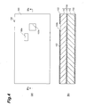
- Fig. 2 is a figure including diagrams showing a manufacturing step of the optical module 1A, that show (a) a plan view of the optical module 1A in the process of manufacturing, and (b) an end elevational view thereof.
- Fig. 3 is a figure including diagrams showing a manufacturing step of the optical module 1A, that show (a) a plan view of the optical module 1A in the process of manufacturing, and (b) an end elevational view thereof.
- Fig. 4 is a figure including diagrams showing a manufacturing step of the optical module 1A, that show (a) a plan view of the optical module 1A in the process of manufacturing, and (b) an end elevational view thereof.
- Fig. 5 is a figure including diagrams showing a manufacturing step of the optical module 1A, that show (a) a plan view of the optical module 1A in the process of manufacturing, and (b) an end elevational view thereof.
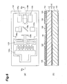
- Fig. 6 is a figure including diagrams showing a manufacturing step of the optical module 1A, that show (a) a plan view of the optical module 1A in the process of manufacturing, and (b) an end elevational view thereof.
- Fig. 7 is a figure including diagrams showing a manufacturing step of the optical module 1A, that show (a) a plan view of the optical module 1A in the process of manufacturing, and (b) an end elevational view thereof.
- Fig. 8 is a figure including diagrams showing a manufacturing step of the optical module 1A, that show (a) a plan view of the optical module 1A in the process of manufacturing, and (b) an end elevational view thereof.
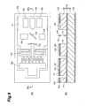
- Fig. 9 is a figure including diagrams showing a manufacturing step of the optical module 1A, that show (a) a plan view of the optical module 1A in the process of manufacturing, and (b) an end elevational view thereof.
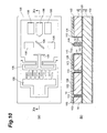
- Fig. 10 is a figure including diagrams showing a manufacturing step of the optical module 1A, that show (a) a plan view of the optical module 1A in the process of manufacturing, and (b) an end elevational view thereof.
- Fig. 11 is a figure including diagrams showing a manufacturing step of the optical module 1A, that show (a) a plan view of the optical module 1A in the process of manufacturing, and (b) an end elevational view thereof.
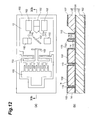
- Fig. 12 is a figure including diagrams showing a manufacturing step of the optical module 1A, that show (a) a plan view of the optical module 1A in the process of manufacturing, and (b) an end elevational view thereof.
- Fig. 13 is a figure including diagrams showing a manufacturing step of the optical module 1A, that show (a) a plan view of the optical module 1A in the process of manufacturing, and (b) an end elevational view thereof.
- Fig. 14 is a figure including diagrams showing a manufacturing step of the optical module 1A, that show (a) a plan view of the optical module 1A in the process of manufacturing, and (b) an end elevational view thereof.
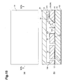
- Fig. 15 is a figure including diagrams showing a manufacturing step of the optical module 1A, that show (a) a plan view of the optical module 1A in the process of manufacturing, and (b) an end elevational view thereof.
- Fig. 16 is a figure including diagrams showing manufacturing steps of the optical module 1A, that show end elevational views of the optical module 1A in the process of manufacturing.
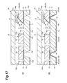
- Fig. 17 is a figure including diagrams showing manufacturing steps of the optical module 1A, that show end elevational views of the optical module 1A in the process of manufacturing.
- Fig. 18 is a figure including diagrams showing manufacturing steps of the optical module 1A, that show end elevational views of the optical module 1A in the process of manufacturing.
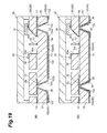
- Fig. 19 is a figure including diagrams showing manufacturing steps of the optical module 1A, that show end elevational views of the optical module 1A in the process of manufacturing.
- Fig. 20 is a diagram showing a manufacturing step of the optical module 1A, that shows an end elevational view of the optical module 1A in the process of manufacturing.
- Fig. 21 is a figure including diagrams showing a configuration of an optical module 1B as a second embodiment of an optical module according to the present invention, that show (a) a plan view of the optical module 1B, and (b) a sectional side view of the optical module 1B taken along the line XXIb-XXIb in (a).
- Fig. 1 shows diagrams showing a configuration of an optical module 1A as a first embodiment of an optical module according to the present invention.
- Fig. 1 shows a perspective view of the optical module 1A
- Fig. 1 shows a sectional side view of the optical module 1A taken along the line Ib-Ib in Fig. 1(a) .
- a cap member 34 included in the optical module 1A is omitted in the illustration to facilitate understanding thereof.
- XYZ orthogonal coordinate systems are shown in Fig. 1(a) and Fig. 1(b) .
- the optical module 1A is manufactured from a substrate product such as an SOI substrate, and the optical module includes a support substrate 10 made of silicon (Si) having a pair of surfaces 10a and 10b, an insulating layer 12 provided on the one surface 10a of the support substrate 10, and a conductive semiconductor layer 14 disposed on the surface 10a of the support substrate 10 via the insulating layer 12.
- the insulating layer 12 is made of, for example, oxide silicon (SiO 2 ), and the semiconductor layer 14 is made of, for example, Si.
- the optical module 1A includes an entrance mirror 16, an optical branching part (beam splitter) 18, a fixed mirror 20, a movable mirror 22, an electrostatic actuator 24, and an element mounting part 26.
- the entrance mirror 16 is primarily composed of a portion of the semiconductor layer 14, and is fixed to the surface 10a of the support substrate 10 via the insulating layer 12.
- the entrance mirror 16 has a mirror surface 16a inclined in the X-axis direction to the surface 10a of the support substrate 10.
- An inclined angle of the mirror surface 16a is, for example, 45 degrees to the surface 10a.
- a light to be measured L 1 is made to enter into the mirror surface 16a from a direction perpendicular to the surface 10a (the Z-axis direction).
- the entrance mirror 16 reflects the light to be measured L 1 to a direction along the surface 10a (the X-axis direction in the present embodiment).
- the optical branching part 18 is primarily composed of a portion of the semiconductor layer 14, and is fixed to the surface 10a of the support substrate 10 via the insulating layer 12.
- the optical branching part 18 is provided in the X-axis direction with a space from the entrance mirror 16.
- the optical branching part 18 has a pair of semireflecting surfaces 18a and 18b extending along the direction perpendicular to the surface 10a of the support substrate 10 (the Z-axis direction).
- the one semireflecting surface 18a is inclined to an optical path of the light to be measured L 1 received from the entrance mirror 16, to reflect a part of the light to be measured L 1 toward the movable mirror 22 which will be described later.
- the semireflecting surface 18a is inclined at 45 degrees to the X-axis direction, and reflects a part of the light to be measured L 1 entering thereinto along the X-axis direction to the Y-axis direction. Further, the semireflecting surface 18a allows the other light to be measured L 1 except for the reflected part of the light to be measured L 1 , to transmit therethrough.
- the fixed mirror 20 is primarily composed of a portion of the semiconductor layer 14, and is fixed to the surface 10a of the support substrate 10 via the insulating layer 12.
- the fixed mirror 20 is provided in the X-axis direction with a space from the entrance mirror 16, and is disposed at a position so as to sandwich the optical branching part 18 with the entrance mirror 16.
- a mirror surface 20a is formed on a side face of the fixed mirror 20 facing the optical branching part 18.
- the mirror surface 20a is optically coupled to the other semireflecting surface 18b of the optical branching part 18.
- the fixed mirror 20 reflects the light to be measured L 1 transmitting through the optical branching part 18 toward the optical branching part 18.
- the reflected light to be measured L 1 is reflected toward the element mounting part 26 which will be described later, by the other semireflecting surface 18b of the optical branching part 18.
- the movable mirror 22 is primarily composed of a portion of the semiconductor layer 14, and is movable in a predetermined direction along the surface 10a (the Y-axis direction in the present embodiment) by eliminating the insulating layer 12 between the portion of the semiconductor layer 14 and the support substrate 10.
- the movable mirror 22 has a side face facing the optical branching part 18 (i.e., a side face intersecting with the above-described predetermined direction), and a mirror surface 22a is formed on the side face.
- the mirror surface 22a is optically coupled to the one semireflecting surface 18a of the optical branching part 18.
- the movable mirror 22 reflects the light to be measured L 1 reflected by the semireflecting surface 18a of the optical branching part 18 toward the optical branching part 18.
- the reflected light to be measured L 1 transmits through the semireflecting surface 18a of the optical branching part 18, to be coupled to the light to be measured L 1 output from the fixed mirror 20 to become an interference optical image L 2 , and the interference optical image goes toward the element mounting part 26.
- the electrostatic actuator 24 is a driving part to displace the movable mirror 22 toward the Y-axis direction.
- the electrostatic actuator 24 has a first electrode 28 fixed to the surface 10a of the support substrate 10 and a second electrode 30 fixed to the movable mirror 22.
- the electrostatic actuator 24 is to generate electrostatic force between the first electrode 28 and the second electrode 30, to relatively displace the second electrode 30 with respect to the first electrode 28.
- the first electrode 28 is disposed on the surface 10a of the support substrate 10.
- the first electrode 28 has a fixed part 28a fixed to the surface 10a of the support substrate 10 via the insulating layer 12, and a comb-structure part 28b formed on a side face of the fixed part 28a facing the second electrode 30.
- the comb part 28b is in a state of floating from the support substrate 10 by eliminating the insulating layer 12 between the portion and the support substrate 10.
- the second electrode 30 is disposed between the movable mirror 22 and the first electrode 28 on the surface 10a of the support substrate 10.
- the second electrode 30 has a columnar support 30a provided to be extended in the Y-axis direction to support the movable mirror 22 with its one end, a comb-structure part 30b which supports the other end of the columnar support 30a and is provided to be extended in the X-axis direction, and a supporting part 30c having a structure in which plate springs are connected, to elastically support the both ends of the comb-structure part 30b.
- the columnar support 30a, the comb part 30b, and the supporting part 30c are in a state of floating from the support substrate 10 by eliminating the insulating layer 12 between the portion and the support substrate 10.
- one end of the supporting part 30c supports the end portion of the comb part 30b, and the other end of the supporting part 30c is fixed to the semiconductor layer 14 remaining on the rim portion of the optical module 1A.
- the columnar support 30a and the comb-structure part 30b are capable of being displaced in the Y-axis direction.
- the comb-structure part 30b faces the comb-structure part 28b of the first electrode 28, and the comb teeth of the comb part 30b are disposed between the respective comb teeth of the comb part 28b.
- electrostatic force is applied between the comb-structure part 30b and the comb-structure part 28b. Because this electrostatic force is determined on the basis of a voltage value applied to the second electrode 30, a distance between the comb-structure part 30b and the comb-structure part 28b is controlled on the basis of the voltage value. That is, the positions in the Y-axis direction of the comb part 28b and the movable mirror 22 supported by the columnar support 30a are controlled on the basis of a voltage applied to the second electrode 30.
- the element mounting part 26 is primarily composed of a portion of the semiconductor layer 14, and is fixed to the surface 10a of the support substrate 10 via the insulating layer 12.
- the element mounting part 26 is a structural member for mounting an optical semiconductor element such as a photodiode 32 thereon, which is provided on the surface 10a of the support substrate 10.
- the element mounting part 26 in the present embodiment is composed of three portions 26a to 26c arrayed in the X-axis direction. Metal films are formed on the top surfaces of these portions 26a to 26c, and the photodiode 32 is installed on these metal films.
- a cathode electrode of the photodiode 32 is conductive-connected to the metal films of the two portions 26a and 26c located on the both ends.
- an anode electrode of the photodiode 32 is conductive-connected to the metal film of the portion 26b located in the center.
- a mirror surface 26d is formed on one of the side faces of the portion 26b located in the center, which faces the movable mirror 22.
- the mirror surface 26d is inclined in the Y-axis direction to the surface 10a of the support substrate 10, and its inclined angle is, for example, 35 degrees to the surface 10a.
- the mirror surface 26d is optically coupled to the semireflecting surface 18b of the optical branching part 18.
- the interference optical image L 2 output from the optical branching part 18 enters into the mirror surface 26d.
- the mirror surface 26d reflects the interference optical image L 2 to the Z-axis direction, to cause the interference optical image to enter into the photodiode 32. That is, the photodiode 32 in the present embodiment is optically coupled to the mirror surface 22a of the movable mirror 22.
- the optical module 1A of the present embodiment further includes a cap member 34, an element electrode part 36, an actuator electrode part 38, and bump electrodes 42 and 44.
- the cap member 34 is provided on the surface 10a of the support substrate 10, and is a member to airtight-seal the interference optical system including the entrance mirror 16, the optical branching part 18, the fixed mirror 20, the movable mirror 22, the electrostatic actuator 24, the element mounting part 26, and the photodiode 32.
- the cap member 34 has a planar shape which is substantially the same as the support substrate 10, and is composed of a top board portion 34a along the surface 10a and a rim portion 34b which is provided on the rim portion of the top board portion 34a, and is connected to the semiconductor layer 14 remaining on the periphery of the interference optical system.
- the cap member 34 (particularly, the top board portion 34a) is formed of a material allowing light having the wavelength of the light to be measured L 1 which is an object of light reception by the photodiode 32 to transmit therethrough. Thereby, it is possible for the light to be measured L 1 input from the outside of the optical module 1A to pass through the top board portion 34a of the cap member 34 to reach the entrance mirror 16.
- the element electrode part 36 is an electrode part to make an electric connection with the photodiode 32.
- the element electrode part 36 is, as shown in Fig. 1(b) , provided through the support substrate 10 and the insulating layer 12 immediately below the element mounting part 26.
- a total of three element electrode parts 36 are singly provided to the respective three portions 26a to 26c of the element mounting part 26, however, the cross section of the element electrode part 36 corresponding to the portion 26b is shown as a representative of those in Fig. 1(b) .
- a through hole 10c is formed in the support substrate 10 and the insulating layer 12, and the upper end of the through hole 10c reaches the portion 26b of the element mounting part 26.
- an insulating film 40 is formed on the inner side face of the through hole 10c, and a metal film serving as the element electrode part 36 is formed on the insulating film 40.
- the end of the element electrode part 36 contacts a portion, which is formed of the semiconductor layer 14, of the portion 26b of the element mounting part 26, and is electrically connected to the anode electrode of the photodiode 32 via the portion 26b.
- the insulating film 40 is formed on the surface 10b of the support substrate 10 as well, and the element electrode part 36 is provided to be partially extended on a partial area of the insulating film 40.
- the actuator electrode part 38 is an electrode part to make an electric connection with the electrostatic actuator 24.
- the actuator electrode part 38 is, as shown in Fig. 1(b) , provided through the support substrate 10 and the insulating layer 12 immediately below the first electrode 28 of the electrostatic actuator 24.
- an actuator electrode part is provided in the same way immediately below the semiconductor layer 14 remaining on the rim portion of the optical module 1A, however, the cross section of the actuator electrode part 38 corresponding to the first electrode 28 is shown as a representative of those in Fig. 1(b) .
- a through hole 10d is formed in the support substrate 10 and the insulating layer 12, and the upper end of the through hole 10d reaches the first electrode 28.
- the insulating film 40 is formed on the inner side face of the through hole 10d, and a metal film serving as the actuator electrode part 38 is formed on the insulating film 40.
- the end of the actuator electrode part 38 contacts a portion, which is formed of the semiconductor layer 14, of the first electrode 28, and is electrically connected to the portion. Further, the actuator electrode part 38 is provided to be partially extended on a partial area of the insulating film 40 formed on the surface 10b.
- the bump electrodes 42 and 44 are provided on the surface 10b of the support substrate 10, and those are respectively electrically connected to the element electrode part 36 and the actuator electrode part 38.
- the bump electrode 42 is formed on a portion, which is formed on the surface 10b, of the element electrode part 36
- the bump electrode 44 is formed on a portion, which is formed on the surface 10b, of the actuator electrode part 38.
- FIGs. 2 to 20 are diagrams showing steps for manufacturing the optical module 1A in order.
- (a) shows a plan view of the optical module 1A in the process of manufacturing
- (b) shows an end elevational view thereof.
- (a) and (b) both show end elevational views of the optical module 1A in the process of manufacturing.
- an SOI substrate 100 is prepared.
- This SOI substrate 100 has the support substrate 10 made of Si, the insulating layer 12 made of SiO 2 , which is provided on the one surface 10a of the support substrate 10, and the semiconductor layer 14 made of Si, which is provided on the insulating layer 12.
- Si oxide films 102 are formed on the surface of the semiconductor layer 14 of the SOI substrate 100 and on the other surface 10b of the support substrate 10.
- the Si on the surfaces of the semiconductor layer 14 and the support substrate 10 be oxidized by use of, for example, wet oxidation method.
- the Si oxide film 102 formed on the surface 10b will become the insulating film 40 shown in Fig. 1 .
- a resist pattern 104 is formed on the Si oxide film 102 formed on the surface of the semiconductor layer 14.
- An opening 104a corresponding to the inclined mirror surface 16a of the entrance mirror 16 shown in Fig. 1(a) , and an opening 104b corresponding to the inclined mirror surface 26d of the element mounting part 26 are formed in the resist pattern 104.
- an Si nitride film 106 is formed on the entire area on the semiconductor layer 14 of the SOI substrate 100.
- SiN be formed as a film on the semiconductor layer 14 (on the Si oxide film 102 for an area on which the Si oxide film 102 is formed) by, for example, an LP-CVD (Low Pressure-Chemical Vapor Deposition) method.
- LP-CVD Low Pressure-Chemical Vapor Deposition
- a resist pattern 108 is formed on the Si nitride film 106.
- a pattern 108a corresponding to the entrance mirror 16 shown in Fig.
- a pattern 108b corresponding to the optical branching part 18 a pattern 108c corresponding to the fixed mirror 20, a pattern 108d corresponding to the movable mirror 22, a pattern 108e corresponding to the first electrode 28 of the electrostatic actuator 24, a pattern 108f corresponding to the second electrode 30 of the electrostatic actuator 24, and patterns 108g to 108i corresponding to the respective portions 26a to 26c of the element mounting part 26 are formed.
- etching is applied to the Si nitride film 106 and the Si oxide film 102 under the Si nitride film via the resist pattern 108.
- a plurality of patterns respectively corresponding to the entrance mirror 16, the optical branching part 18, the fixed mirror 20, the movable mirror 22, the electrostatic actuator 24 (the first electrode 28 and the second electrode 30), and the respective portions 26a to 26c of the element mounting part 26 are formed in the Si nitride film 106 and the Si oxide film 102.
- Si oxide films 110 are formed on the side faces of the semiconductor layer 14 in order to protect the exposed side faces of the semiconductor layer 14. At this time, it is preferable that the Si on the exposed side faces of the semiconductor layer 14 be oxidized by use of, for example, wet oxidation method.
- the Si nitride film 106 is eliminated.
- the etching is applied only to the Si nitride film 106 selectively so as to leave the Si oxide film 102 by use of, for example, hot phosphoric acid (heated phosphoric acid solution) or the like.
- the opening in the Si oxide film 102 corresponding to the inclined mirror surface 16a of the entrance mirror 16 and the opening in the Si oxide film 102 corresponding to the inclined mirror surface 26d of the element mounting part 26 make their appearances again, and the semiconductor layer 14 on the corresponding portions is exposed.
- a shadow mask 114 is disposed so as to cover the surface 10a side of the support substrate 10.
- openings 114a corresponding to the portion which will be the mirror surface 16a in the entrance mirror 16, the portion which will be the mirror surface 20a in the fixed mirror 20, the portion which will be the mirror surface 22a in the movable mirror 22, and the entire element mounting part 26 are formed. Then, physical vapor deposition or the like of a metal material is applied via the shadow mask 114 thereto, to form metal films on the above-described respective portions. Thereby, the mirror surfaces 16a, 20a, 22a, and 26d, and the metal films 116 on the element mounting part 26 are formed. Thereafter, the shadow mask 114 is eliminated.
- the photodiode 32 is installed on the element mounting part 26. Then, the surface 10a side of the support substrate 10 is covered with the cap member 34. At this time, the rim portion 34b of the cap member 34 and the top surface of the semiconductor layer 14 remaining on the rim portion of the surface 10a of the support substrate 10 are connected to each other, to airtight-seal up the interference optical system including the movable mirror 22 and the photodiode 32.
- a resist pattern 118 is formed on the Si oxide film 102 formed on the surface 10b of the support substrate 10.
- An opening 118a corresponding to the through hole 10c shown in Fig. 1(b) and an opening 118b corresponding to the through hole 10d are formed in the resist pattern 118.
- the insulating films 40 are formed on the inner side faces of the through holes 10c and 10d in the support substrate 10. At this time, it is preferable that Si oxide films be formed by, for example, a TEOS-CVD method using tetraethoxysilane as the insulating films 40.
- a resist pattern 120 is formed on the Si oxide film 102 (the insulating film 40) formed on the surface 10b of the support substrate 10 and the insulating films 40 formed on the inner side faces of the through holes 10c and 10d.
- the resist pattern 120 is formed by, for example, spray coating, and has openings 120a and 120b respectively in the portions corresponding to the ends of the through holes 10c and 10d.
- dry etching is applied thereto via the resist pattern 120, to form through holes in the insulating films 40 and the insulating layers 12 as shown in (b) in Fig. 18 . Thereby, the semiconductor layers 14 in the element mounting part 26 and the first electrode 28 are exposed. Thereafter, the resist pattern 120 is eliminated.
- a resist pattern 122 is formed on the Si oxide film 102 (the insulating film 40) formed on the surface 10b of the support substrate 10 by, for example, spray coating.
- the resist pattern 122 has openings 122a and 122b through which the through holes 10c and 10d and the insulating films 40 formed on the peripheral portions thereof are exposed.
- metal films are formed on the insulating films 40 by a liftoff technology utilizing the resist pattern 122. This metal films are the element electrode part 36 and the actuator electrode part 38 shown in (b) in Fig. 19 .
- the bump electrodes 42 and 44 are formed on the portions, which are formed on the Si oxide films 102 (the insulating films 40), of the element electrode part 36 and the actuator electrode part 38. In this way, the optical module 1A shown in Fig. 1 is completed.
- the photodiode 32 is provided on the support substrate 10, and the photodiode 32 and the movable mirror 22 are together airtight-sealed with the cap member 34. Then, the photodiode 32 and the mirror surface 22a of the movable mirror 22 are optically coupled.
- the photodiode 32 is provided on the support substrate 10, there is no need to provide a photodetector or the like outside the device, which makes it possible to downsize the module.
- a wiring pattern is formed on the support substrate 10, to be led out to the outside of the package of the module.
- the airtightness of the optical system including the movable mirror 22 may be deteriorated due to the irregularity generated by such a wiring.
- the element electrode part 36 electrically connected to the photodiode 32 is provided through the support substrate 10 and the insulating layer 12.
- the photodiode 32 is energized from above the surface 10b of the support substrate 10, and therefore, there is no need to lead out a wiring pattern on the surface 10a of the support substrate 10, and it is possible to further enhance the airtightness of the optical system including the movable mirror 22 with the cap member 34.
- the optical module 1A may include the electrostatic actuator 24 that drives the movable mirror 22 by electrostatic force generated between the first electrode 28 and the second electrode 30, and the actuator electrode part 38 which is provided through the support substrate 10 and the insulating layer 12.
- the electrostatic actuator 24 having such a configuration is configured on the support substrate 10, it is possible to favorably drive the minute movable mirror 22.
- the cap member 34 is preferably formed of a material that allows the light to be measured L 1 , which is an object of light reception by the photodiode 32 to transmit through the cap member. Thereby, it is possible to input the light to be measured L 1 via the cap member 34 at the surface 10a side of the support substrate 10. Accordingly, there is no need to install a component such as an optical fiber for optical input on the surface 10a of the support substrate 10, and it is possible to further enhance the airtightness of the interference optical system including the movable mirror 22.
- the element mounting part 26 including a portion of the semiconductor layer 14, on which the photodiode 32 is mounted is provided, and the end of the element electrode part 36 contacts the portion of the semiconductor layer 14 in the element mounting part 26.
- the optical module 1A includes the element mounting part 26, it is possible to install the photodiode 32 on the support substrate 10 by flip-chip configuration, and therefore, wire bonding for energizing the photodiode 32 is unneeded, which makes it easy to handle the support substrate 10 and the like during manufacturing. Further, because the portion of the semiconductor layer 14 in the element mounting part 26 and the element electrode part 36 contact each other, it is possible to easily achieve an electric connection between the element electrode part 36 and the photodiode 32.
- the optical module 1A includes the bump electrode 42 which is provided on the surface 10b of the support substrate 10, to be electrically connected to the element electrode part 36.
- the optical module 1A it is possible to install the optical module 1A onto a wiring substrate or the like by a simple method such as a reflow method.
- the cap member 34 is attached after the driving portions such as the movable mirror 22 and the second electrode 30 are formed, a wet process is not carried out in order to prevent difficulties in operations of the driving portions due to moisture. Accordingly, at the time of forming metal films, a method using a shadow mask is mainly used, however, this method has low dimensional accuracy, which makes it difficult to achieve minute wiring formation.
- a function as a wiring is provided by physically isolating the conductive semiconductor layers 14, and because etching onto the semiconductor layer 14 is possible even with a minute line width of several tens of ⁇ m, most normal optical semiconductor elements can be installed.
- the element electrode part 36 and the actuator electrode part 38 on the surface 10b are provided for interfacing to the outside, and therefore, minute accuracy is not required.
- Fig. 21 shows diagrams showing a configuration of an optical module 1B as a second embodiment of an optical module according to the present invention.
- Fig. 21 shows a plan view of the optical module 1B
- Fig. 21 shows a sectional side view of the optical module 1B taken along the line XXIb-XXIb in Fig. 21(a) .
- the cap member 34 included in the optical module 1B is omitted in the illustration to facilitate understanding thereof.
- XYZ orthogonal coordinate systems are shown in Fig. 21(a) and Fig. 2(b) .
- the optical module 1B of the present embodiment is manufactured from an SOI substrate in the same way as the optical module 1A of the first embodiment, and the optical module includes the support substrate 10, the insulating layer 12, and the semiconductor layer 14. Further, the movable mirror 22 and the electrostatic actuator 24 as parts of the structural members for constituting a Michelson interference optical system are formed in the insulating layer 12 and the semiconductor layer 14. Moreover, the optical module 1B includes the cap member 34, the actuator electrode part 38, and the bump electrode 44. The configurations of those are the same as those in the first embodiment, and detailed descriptions thereof will be omitted.
- the optical module 1B according to the present embodiment includes an optical structural member 52 and an element mounting part 54 in place of the entrance mirror 16, the optical branching part 18, the fixed mirror 20, and the element mounting part 26 in the first embodiment. Further, a light pass-through hole 10e is formed in a portion of the support substrate 10 located immediately below the optical structural member 52. The light pass-through hole 10e is provided through the support substrate 10 and the insulating layer 12, and a light to be measured L 3 is input via the light pass-through hole 10e.
- the optical structural member 52 is a structural member having the functions of the entrance mirror 16, the optical branching part 18, and the fixed mirror 20 in the first embodiment all together.
- the optical structural member 52 is primarily composed of a portion of the semiconductor layer 14, and is fixed to the surface 10a of the support substrate 10 via the insulating layer 12.
- a mirror surface 52a inclined to the surface 10a of the support substrate 10 and a semireflecting surface 52b and a mirror surface 52c extending in a direction perpendicular to the surface 10a (the Z-axis direction) are formed on the side faces of the optical structural member 52.
- An inclined angle of the mirror surface 52a is, for example, 45 degrees to the surface 10a.
- the light to be measured L 3 passing through the light pass-through hole 10e formed in the support substrate 10 to transmit through the inside of the optical structural member 52, reaches the mirror surface 52a.
- the mirror surface 52a reflects the light to be measured L 3 toward the semireflecting surface 52b in plane along the surface 10a.
- the semireflecting surface 52b is optically coupled to the mirror surfaces 52a and 52c, the mirror surface 22a of the movable mirror 22, and the element mounting part 54.
- the semireflecting surface 52b reflects a part of the light to be measured L 3 entering thereinto via the mirror surface 52a toward the mirror surface 52c. Further, the semireflecting surface 52b allows the other light to be measured L 3 except for the reflected part of the light to be measured L 3 , to transmit therethrough toward the movable mirror 22.
- the movable mirror 22 reflects the light to be measured L 3 transmitting through the semireflecting surface 52b toward the semireflecting surface 52b. The light to be measured L 3 is reflected by the semireflecting surface 52b toward the element mounting part 54.
- the mirror surface 52c reflects the light to be measured L 3 reflected by the semireflecting surface 52b, toward the semireflecting surface 52b.
- the light to be measured L 3 transmits through the semireflecting surface 52b toward the element mounting part 54, to be coupled to the light to be measured L 3 reaching there from the movable mirror 22 to become an interference optical image L 4 .
- the element mounting part 54 has the same structure as the element mounting part 26 in the first embodiment, and its layout and orientation are different from those in the first embodiment. That is, the element mounting part 54 is a structural member for mounting an optical semiconductor element such as a photodiode 32 thereon, and is composed of three portions 54a to 54c arrayed in a given direction. Metal films are formed on the top surfaces of these portions 54a to 54c, and the photodiode 32 is installed on these metal films.
- an element electrode part as well which has the same structure as the element electrode part 36 in the first embodiment, is provided immediately below the element mounting part 54.
- a mirror surface inclined to the surface 10a is formed on a side face facing the semireflecting surface 52b among the side faces of the portion 54b.
- the interference optical image L 4 output from the semireflecting surface 52b enters into this mirror surface.
- This mirror surface reflects the interference optical image L 4 toward the Z-axis direction to provide it to the photodiode 32.
- the same advantageous effects which are the same as those of the optical module 1A according to the first embodiment can be obtained. That is, because the photodiode 32 and the movable mirror 22 are together airtight-sealed with the cap member 34, there is no need to install an optical fiber for connecting to an external detector or the like, and therefore, it is possible to enhance the airtightness of the interference optical system including the movable mirror 22 with the cap member 34. Further, because the photodiode 32 is provided on the support substrate 10, there is no need to provide a photodetector or the like outside the device, which makes it possible to downsize the module.
- the module may be configured such that the light to be measured L 3 received by the photodiode 32 is input via the light pass-through hole 10e provided through the support substrate 10 and the insulating layer 12. Thereby, it is possible to input the light to be measured L 3 from the surface 10b side of the support substrate 10. Accordingly, there is no need to install a component such as an optical fiber for optical input on the surface 10a of the support substrate 10, and it is possible to further enhance the airtightness of the interference optical system including the movable mirror 22.
- the light pass-through hole 10e is formed so as to penetrate through the insulating layer 12 as in the present embodiment, it is possible to avoid the light to be measured L 3 from being reflected by the insulating layer 12, to enhance the use efficiency of the light to be measured L 3 .
- the optical module according to the present invention is not limited to the above-described embodiments, and various modifications thereof are possible.
- the photodiode that is a light receiving element is exemplified as an optical semiconductor element included in the optical module, however, the optical module according to the present invention may include a light emitting element as an optical semiconductor element.
- the lights to be measured L 1 and L 3 and the interference optical images L 2 and L 4 in above-described respective embodiments are replaced by a light emitted from the light emitting element. That is, a light emitted from the light emitting element transmits through the cap member 34 to be output in the first embodiment, and a light emitted from the light emitting element passes through the light pass-through hole 10e to be output in the second embodiment.
- the interference optical system is exemplified as an optical system included in the optical module, however, the optical module according to the present invention may include any optical system with a movable mirror and an optical semiconductor element, which even has another configuration.
- a nitride film (Si 3 N 4 ) may be formed to have a thickness of ⁇ /4n ( ⁇ : wavelength of light to be measured, n: refractive index of nitride film) on these surfaces.
- the optical module is an optical module which is manufactured from a substrate product having a support substrate and a semiconductor layer disposed on one surface of the support substrate via an insulating layer, the optical module including a movable mirror which includes a portion of the semiconductor layer, and in which a mirror surface is formed on a side face intersecting with a predetermined direction, the movable mirror is movable in the predetermined direction along the one surface by eliminating the insulating layer between the portion and the support substrate, an optical semiconductor element which is provided on the one surface of the support substrate, and is optically coupled to the mirror surface of the movable mirror, a cap member which is provided on the one surface of the support substrate, the cap member airtight-seals the movable mirror and the optical semiconductor element, and an electrode part for element which is provided so as to penetrate through the support substrate and the insulating layer, and is electrically connected to the optical semiconductor element.
- the optical module may be configured to further include an electrostatic actuator which has a first electrode fixed to the support substrate and a second electrode fixed to the movable mirror, the electrostatic actuator drives the movable mirror by electrostatic force generated between the first electrode and the second electrode, and an electrode part for actuator which is provided so as to penetrate through the support substrate and the insulating layer, and is electrically connected to the first electrode.
- an electrostatic actuator which has a first electrode fixed to the support substrate and a second electrode fixed to the movable mirror, the electrostatic actuator drives the movable mirror by electrostatic force generated between the first electrode and the second electrode, and an electrode part for actuator which is provided so as to penetrate through the support substrate and the insulating layer, and is electrically connected to the first electrode.
- the electrostatic actuator having such a configuration is configured on the support substrate, it is possible to favorably drive the minute movable mirror.
- the optical module may be configured such that the cap member is formed of a material that allows a light received or emitted by the optical semiconductor element to transmit through the cap member. Thereby, it is possible to input or output an entering light or an emitted light via the cap member at the one surface side of the support substrate.
- the optical module may be configured to have a light pass-through hole penetrating through the support substrate and the insulating layer, and a light received or emitted by the optical semiconductor element is input or output via the light pass-through hole. Thereby, it is possible to input or output an entering light or an emitted light via the light pass-through hole at the other surface side of the support substrate.
- the optical module further includes one of those configurations, there is no need to install a component such as an optical fiber for optical input or optical output on the one surface of the support substrate, and it is possible to further enhance the airtightness of the optical system including the movable mirror.
- the optical module may be configured to further include a fixed mirror which includes a portion of the semiconductor layer, and in which a mirror surface is formed on one side face, the fixed mirror is fixed on the one surface of the support substrate, and a beam splitter which includes a portion of the semiconductor layer, and in which one surface is optically coupled to the mirror surface of the movable mirror, and the other surface is optically coupled to the mirror surface of the fixed mirror, and the mirror surface of the movable mirror, the mirror surface of the fixed mirror, and the beam splitter constitute an interferometer.
- the optical module may be configured to further include an element mounting part including a portion of the semiconductor layer, on which the optical semiconductor element is mounted, and a leading end of the electrode part for element is in contact with the portion of the semiconductor layer in the element mounting part.
- an element mounting part including a portion of the semiconductor layer, on which the optical semiconductor element is mounted, and a leading end of the electrode part for element is in contact with the portion of the semiconductor layer in the element mounting part.
- the optical module may be configured to further include a bump electrode which is provided on the other surface of the support substrate, and is electrically connected to the electrode part for element.
- a bump electrode which is provided on the other surface of the support substrate, and is electrically connected to the electrode part for element.
- the present invention can be utilized as an optical module which is capable of enhancing the airtightness of an optical system including a movable mirror, and which also can be downsized.
Landscapes
- Engineering & Computer Science (AREA)
- Microelectronics & Electronic Packaging (AREA)
- Computer Hardware Design (AREA)
- Physics & Mathematics (AREA)
- General Physics & Mathematics (AREA)
- Mechanical Light Control Or Optical Switches (AREA)
- Micromachines (AREA)
- Instruments For Measurement Of Length By Optical Means (AREA)
- Semiconductor Lasers (AREA)
Abstract
Description
- The present invention relates to an optical module using a MEMS (Micro Electro Mechanical Systems) technology.
- In recent years, the development of MEMS devices manufactured by use of the MEMS technology has been advanced, and such MEMS devices can be put into practice as various optical components.
- For example, in Patent Document 1, there is disclosed an interference optical system which is configured on an SOI (Silicon On Insulator) substrate by use of the MEMS technology. The interference optical system according to Patent Document 1 includes a beam splitter, a movable mirror attached to an electrostatic actuator, and a fixed mirror, and these are formed by applying etching to a silicon layer and an insulating layer of an SOI substrate into arbitrary shapes. Then, a groove for installing an optical fiber therein is formed on the SOI substrate, and an interference light image generated by the interference optical system is led out to the outside via the optical fiber installed in the groove.
- Patent Document 1: Japanese Patent Application Laid-Open No.
2008-102132 - However, there are the following problems in the configuration described in Patent Document 1. That is, an interference optical image generated by the interference optical system is taken out via the optical fiber, and for this purpose, it is necessary to connect a photodetector to the optical fiber outside the device. Therefore, the entire apparatus is made larger in size. Further, because a driving part such as a movable mirror has a shape in dimensions from several µm to several tens of µm, that is minute, malfunction is easily caused therein due to dust, water droplets, and the like being adhered to a gap between the movable mirror and the substrate. Accordingly, in order to prevent invasion of dust, water droplets, and the like, an optical system including a movable mirror is preferably airtight-sealed, however, in a configuration in which an output light such as an interference optical image is taken out via an optical fiber, it is difficult to sufficiently secure the airtightness in the vicinity of the optical fiber.
- The present invention has been achieved in consideration of the above-described problems, and an object of the present invention is to provide an optical module which is capable of enhancing the airtightness of an optical system including a movable mirror, and which can also be downsized.
- In order to solve the above-described problems, there is provided an optical module according to the present invention, which is manufactured from a substrate product having a support substrate and a semiconductor layer disposed on one surface of the support substrate via an insulating layer, the optical module including a movable mirror which includes a portion of the semiconductor layer, and in which a mirror surface is formed on a side face intersecting with a predetermined direction, the movable mirror is movable in the predetermined direction along the one surface by eliminating the insulating layer between the portion of the semiconductor layer and the support substrate, an optical semiconductor element which is provided on the one surface of the support substrate, and is optically coupled to the mirror surface of the movable mirror, a cap member which is provided on the one surface of the support substrate, the cap member airtight-seals the movable mirror and the optical semiconductor element, and an element electrode part which is provided through the support substrate and the insulating layer, and is electrically connected to the optical semiconductor element.
- In the optical module according to the present invention, the optical semiconductor element is provided on the support substrate, and the optical semiconductor element and the movable mirror are together airtight-sealed with the cap member. Then, the optical semiconductor element and the mirror surface of the movable mirror are optically coupled to one another. In accordance with such a configuration, there is no need to install an optical fiber for connecting to an external detector or the like as included in the device, that is disclosed in above-described Patent Document 1, and therefore, it is possible to enhance the airtightness of the optical system including the movable mirror with the cap member. Further, because the optical semiconductor element is provided on the support substrate, there is no need to provide a photodetector or the like outside the device, which makes it possible to downsize the module.
- Further, in the case in which it is necessary to make electric connections with the structural members or electric elements on the support substrate, generally, a wiring pattern is formed on the support substrate, to be led out to the outside of the package of the module. However, the airtightness of the optical system including the movable mirror may be deteriorated due to the irregularity generated by such a wiring. There is also a method in which a place contacting the cap member is covered with an insulating film, and the insulating film is ground to flatten the contacting surface with the cap member, however, not only is the number of steps increased, but also, in some cases, it may be impossible to utilize such a method depending on a type of device. In contrast thereto, in the optical module according to the present invention, the element electrode part electrically connected to the optical semiconductor element is provided through the support substrate and the insulating layer. Thereby, it is possible to make an electric connection with the optical semiconductor element from above the other surface of the support substrate, and therefore, there is no need to lead out a wiring pattern on the one surface of the support substrate, and it is possible to further enhance the airtightness of the optical system including the movable mirror with the cap member.
- In accordance with the above-described optical module, it is possible to enhance the airtightness of the optical system including the movable mirror, and to downsize the module.
- The present invention will be more fully understood from the detailed description given hereinbelow and the accompanying drawings, which are given by way of illustration only and are not to be considered as limiting the present invention.
- Further scope of applicability of the present invention will become apparent from the detailed description given hereinafter. However, it should be understood that the detailed description and specific examples, while indicating preferred embodiments of the invention, are given by way of illustration only, since various changes and modifications within the spirit and scope of the invention will be apparent to those skilled in the art from this detailed description.
-
Fig. 1 is a figure including diagrams showing a configuration of anoptical module 1A as a first embodiment of an optical module according to the present invention, that show (a) a perspective view of theoptical module 1A, and (b) a sectional side view of theoptical module 1A taken along the line Ib-Ib in (a). -
Fig. 2 is a figure including diagrams showing a manufacturing step of theoptical module 1A, that show (a) a plan view of theoptical module 1A in the process of manufacturing, and (b) an end elevational view thereof. -
Fig. 3 is a figure including diagrams showing a manufacturing step of theoptical module 1A, that show (a) a plan view of theoptical module 1A in the process of manufacturing, and (b) an end elevational view thereof. -
Fig. 4 is a figure including diagrams showing a manufacturing step of theoptical module 1A, that show (a) a plan view of theoptical module 1A in the process of manufacturing, and (b) an end elevational view thereof. -
Fig. 5 is a figure including diagrams showing a manufacturing step of theoptical module 1A, that show (a) a plan view of theoptical module 1A in the process of manufacturing, and (b) an end elevational view thereof. -
Fig. 6 is a figure including diagrams showing a manufacturing step of theoptical module 1A, that show (a) a plan view of theoptical module 1A in the process of manufacturing, and (b) an end elevational view thereof. -
Fig. 7 is a figure including diagrams showing a manufacturing step of theoptical module 1A, that show (a) a plan view of theoptical module 1A in the process of manufacturing, and (b) an end elevational view thereof. -
Fig. 8 is a figure including diagrams showing a manufacturing step of theoptical module 1A, that show (a) a plan view of theoptical module 1A in the process of manufacturing, and (b) an end elevational view thereof. -
Fig. 9 is a figure including diagrams showing a manufacturing step of theoptical module 1A, that show (a) a plan view of theoptical module 1A in the process of manufacturing, and (b) an end elevational view thereof. -
Fig. 10 is a figure including diagrams showing a manufacturing step of theoptical module 1A, that show (a) a plan view of theoptical module 1A in the process of manufacturing, and (b) an end elevational view thereof. -
Fig. 11 is a figure including diagrams showing a manufacturing step of theoptical module 1A, that show (a) a plan view of theoptical module 1A in the process of manufacturing, and (b) an end elevational view thereof. -
Fig. 12 is a figure including diagrams showing a manufacturing step of theoptical module 1A, that show (a) a plan view of theoptical module 1A in the process of manufacturing, and (b) an end elevational view thereof. -
Fig. 13 is a figure including diagrams showing a manufacturing step of theoptical module 1A, that show (a) a plan view of theoptical module 1A in the process of manufacturing, and (b) an end elevational view thereof. -
Fig. 14 is a figure including diagrams showing a manufacturing step of theoptical module 1A, that show (a) a plan view of theoptical module 1A in the process of manufacturing, and (b) an end elevational view thereof. -
Fig. 15 is a figure including diagrams showing a manufacturing step of theoptical module 1A, that show (a) a plan view of theoptical module 1A in the process of manufacturing, and (b) an end elevational view thereof. -
Fig. 16 is a figure including diagrams showing manufacturing steps of theoptical module 1A, that show end elevational views of theoptical module 1A in the process of manufacturing. -
Fig. 17 is a figure including diagrams showing manufacturing steps of theoptical module 1A, that show end elevational views of theoptical module 1A in the process of manufacturing. -
Fig. 18 is a figure including diagrams showing manufacturing steps of theoptical module 1A, that show end elevational views of theoptical module 1A in the process of manufacturing. -
Fig. 19 is a figure including diagrams showing manufacturing steps of theoptical module 1A, that show end elevational views of theoptical module 1A in the process of manufacturing. -
Fig. 20 is a diagram showing a manufacturing step of theoptical module 1A, that shows an end elevational view of theoptical module 1A in the process of manufacturing. -
Fig. 21 is a figure including diagrams showing a configuration of anoptical module 1B as a second embodiment of an optical module according to the present invention, that show (a) a plan view of theoptical module 1B, and (b) a sectional side view of theoptical module 1B taken along the line XXIb-XXIb in (a). - Hereinafter, embodiments of an optical module according to the present invention will be described in detail with reference to the accompanying drawings. Note that, in the descriptions of the drawings, same components are denoted by same reference numerals and letters, and overlapping descriptions will be omitted.
-
Fig. 1 shows diagrams showing a configuration of anoptical module 1A as a first embodiment of an optical module according to the present invention. Here, (a) inFig. 1 shows a perspective view of theoptical module 1A, and (b) inFig. 1 shows a sectional side view of theoptical module 1A taken along the line Ib-Ib inFig. 1(a) . Note that, inFig. 1(a) , acap member 34 included in theoptical module 1A is omitted in the illustration to facilitate understanding thereof. Further, XYZ orthogonal coordinate systems are shown inFig. 1(a) and Fig. 1(b) . - The
optical module 1A is manufactured from a substrate product such as an SOI substrate, and the optical module includes asupport substrate 10 made of silicon (Si) having a pair ofsurfaces insulating layer 12 provided on the onesurface 10a of thesupport substrate 10, and aconductive semiconductor layer 14 disposed on thesurface 10a of thesupport substrate 10 via theinsulating layer 12. Theinsulating layer 12 is made of, for example, oxide silicon (SiO2), and thesemiconductor layer 14 is made of, for example, Si. - A plurality of structural members for constituting a Michelson interference optical system are formed in the
insulating layer 12 and thesemiconductor layer 14. That is, theoptical module 1A includes anentrance mirror 16, an optical branching part (beam splitter) 18, afixed mirror 20, amovable mirror 22, anelectrostatic actuator 24, and anelement mounting part 26. - The
entrance mirror 16 is primarily composed of a portion of thesemiconductor layer 14, and is fixed to thesurface 10a of thesupport substrate 10 via theinsulating layer 12. Theentrance mirror 16 has amirror surface 16a inclined in the X-axis direction to thesurface 10a of thesupport substrate 10. An inclined angle of themirror surface 16a is, for example, 45 degrees to thesurface 10a. A light to be measured L1 is made to enter into themirror surface 16a from a direction perpendicular to thesurface 10a (the Z-axis direction). Theentrance mirror 16 reflects the light to be measured L1 to a direction along thesurface 10a (the X-axis direction in the present embodiment). - The optical branching
part 18 is primarily composed of a portion of thesemiconductor layer 14, and is fixed to thesurface 10a of thesupport substrate 10 via the insulatinglayer 12. The optical branchingpart 18 is provided in the X-axis direction with a space from theentrance mirror 16. The optical branchingpart 18 has a pair ofsemireflecting surfaces surface 10a of the support substrate 10 (the Z-axis direction). The one semireflectingsurface 18a is inclined to an optical path of the light to be measured L1 received from theentrance mirror 16, to reflect a part of the light to be measured L1 toward themovable mirror 22 which will be described later. In the present embodiment, thesemireflecting surface 18a is inclined at 45 degrees to the X-axis direction, and reflects a part of the light to be measured L1 entering thereinto along the X-axis direction to the Y-axis direction. Further, thesemireflecting surface 18a allows the other light to be measured L1 except for the reflected part of the light to be measured L1, to transmit therethrough. - The fixed
mirror 20 is primarily composed of a portion of thesemiconductor layer 14, and is fixed to thesurface 10a of thesupport substrate 10 via the insulatinglayer 12. The fixedmirror 20 is provided in the X-axis direction with a space from theentrance mirror 16, and is disposed at a position so as to sandwich the optical branchingpart 18 with theentrance mirror 16. Amirror surface 20a is formed on a side face of the fixedmirror 20 facing the optical branchingpart 18. Themirror surface 20a is optically coupled to theother semireflecting surface 18b of the optical branchingpart 18. The fixedmirror 20 reflects the light to be measured L1 transmitting through the optical branchingpart 18 toward the optical branchingpart 18. The reflected light to be measured L1 is reflected toward theelement mounting part 26 which will be described later, by theother semireflecting surface 18b of the optical branchingpart 18. - The
movable mirror 22 is primarily composed of a portion of thesemiconductor layer 14, and is movable in a predetermined direction along thesurface 10a (the Y-axis direction in the present embodiment) by eliminating the insulatinglayer 12 between the portion of thesemiconductor layer 14 and thesupport substrate 10. Themovable mirror 22 has a side face facing the optical branching part 18 (i.e., a side face intersecting with the above-described predetermined direction), and amirror surface 22a is formed on the side face. Themirror surface 22a is optically coupled to the onesemireflecting surface 18a of the optical branchingpart 18. Themovable mirror 22 reflects the light to be measured L1 reflected by thesemireflecting surface 18a of the optical branchingpart 18 toward the optical branchingpart 18. The reflected light to be measured L1 transmits through thesemireflecting surface 18a of the optical branchingpart 18, to be coupled to the light to be measured L1 output from the fixedmirror 20 to become an interference optical image L2, and the interference optical image goes toward theelement mounting part 26. - The
electrostatic actuator 24 is a driving part to displace themovable mirror 22 toward the Y-axis direction. Theelectrostatic actuator 24 has afirst electrode 28 fixed to thesurface 10a of thesupport substrate 10 and asecond electrode 30 fixed to themovable mirror 22. Theelectrostatic actuator 24 is to generate electrostatic force between thefirst electrode 28 and thesecond electrode 30, to relatively displace thesecond electrode 30 with respect to thefirst electrode 28. - The
first electrode 28 is disposed on thesurface 10a of thesupport substrate 10. Thefirst electrode 28 has a fixedpart 28a fixed to thesurface 10a of thesupport substrate 10 via the insulatinglayer 12, and a comb-structure part 28b formed on a side face of thefixed part 28a facing thesecond electrode 30. Here, thecomb part 28b is in a state of floating from thesupport substrate 10 by eliminating the insulatinglayer 12 between the portion and thesupport substrate 10. - The
second electrode 30 is disposed between themovable mirror 22 and thefirst electrode 28 on thesurface 10a of thesupport substrate 10. Thesecond electrode 30 has acolumnar support 30a provided to be extended in the Y-axis direction to support themovable mirror 22 with its one end, a comb-structure part 30b which supports the other end of thecolumnar support 30a and is provided to be extended in the X-axis direction, and a supportingpart 30c having a structure in which plate springs are connected, to elastically support the both ends of the comb-structure part 30b. Thecolumnar support 30a, thecomb part 30b, and the supportingpart 30c are in a state of floating from thesupport substrate 10 by eliminating the insulatinglayer 12 between the portion and thesupport substrate 10. Further, one end of the supportingpart 30c supports the end portion of thecomb part 30b, and the other end of the supportingpart 30c is fixed to thesemiconductor layer 14 remaining on the rim portion of theoptical module 1A. In accordance with such a configuration, thecolumnar support 30a and the comb-structure part 30b are capable of being displaced in the Y-axis direction. The comb-structure part 30b faces the comb-structure part 28b of thefirst electrode 28, and the comb teeth of thecomb part 30b are disposed between the respective comb teeth of thecomb part 28b. - When a predetermined voltage is applied to the
second electrode 30, electrostatic force is applied between the comb-structure part 30b and the comb-structure part 28b. Because this electrostatic force is determined on the basis of a voltage value applied to thesecond electrode 30, a distance between the comb-structure part 30b and the comb-structure part 28b is controlled on the basis of the voltage value. That is, the positions in the Y-axis direction of thecomb part 28b and themovable mirror 22 supported by thecolumnar support 30a are controlled on the basis of a voltage applied to thesecond electrode 30. - The
element mounting part 26 is primarily composed of a portion of thesemiconductor layer 14, and is fixed to thesurface 10a of thesupport substrate 10 via the insulatinglayer 12. Theelement mounting part 26 is a structural member for mounting an optical semiconductor element such as aphotodiode 32 thereon, which is provided on thesurface 10a of thesupport substrate 10. Theelement mounting part 26 in the present embodiment is composed of threeportions 26a to 26c arrayed in the X-axis direction. Metal films are formed on the top surfaces of theseportions 26a to 26c, and thephotodiode 32 is installed on these metal films. For example, a cathode electrode of thephotodiode 32 is conductive-connected to the metal films of the twoportions photodiode 32 is conductive-connected to the metal film of theportion 26b located in the center. - Further, a
mirror surface 26d is formed on one of the side faces of theportion 26b located in the center, which faces themovable mirror 22. Themirror surface 26d is inclined in the Y-axis direction to thesurface 10a of thesupport substrate 10, and its inclined angle is, for example, 35 degrees to thesurface 10a. Themirror surface 26d is optically coupled to thesemireflecting surface 18b of the optical branchingpart 18. The interference optical image L2 output from the optical branchingpart 18 enters into themirror surface 26d. Themirror surface 26d reflects the interference optical image L2 to the Z-axis direction, to cause the interference optical image to enter into thephotodiode 32. That is, thephotodiode 32 in the present embodiment is optically coupled to themirror surface 22a of themovable mirror 22. - In addition to the configuration described above, the
optical module 1A of the present embodiment further includes acap member 34, anelement electrode part 36, anactuator electrode part 38, and bumpelectrodes - The
cap member 34 is provided on thesurface 10a of thesupport substrate 10, and is a member to airtight-seal the interference optical system including theentrance mirror 16, the optical branchingpart 18, the fixedmirror 20, themovable mirror 22, theelectrostatic actuator 24, theelement mounting part 26, and thephotodiode 32. Thecap member 34 has a planar shape which is substantially the same as thesupport substrate 10, and is composed of atop board portion 34a along thesurface 10a and arim portion 34b which is provided on the rim portion of thetop board portion 34a, and is connected to thesemiconductor layer 14 remaining on the periphery of the interference optical system. The cap member 34 (particularly, thetop board portion 34a) is formed of a material allowing light having the wavelength of the light to be measured L1 which is an object of light reception by thephotodiode 32 to transmit therethrough. Thereby, it is possible for the light to be measured L1 input from the outside of theoptical module 1A to pass through thetop board portion 34a of thecap member 34 to reach theentrance mirror 16. - The element electrode
part 36 is an electrode part to make an electric connection with thephotodiode 32. The element electrodepart 36 is, as shown inFig. 1(b) , provided through thesupport substrate 10 and the insulatinglayer 12 immediately below theelement mounting part 26. Here, a total of threeelement electrode parts 36 are singly provided to the respective threeportions 26a to 26c of theelement mounting part 26, however, the cross section of theelement electrode part 36 corresponding to theportion 26b is shown as a representative of those inFig. 1(b) . - In detail, a through
hole 10c is formed in thesupport substrate 10 and the insulatinglayer 12, and the upper end of the throughhole 10c reaches theportion 26b of theelement mounting part 26. Then, an insulatingfilm 40 is formed on the inner side face of the throughhole 10c, and a metal film serving as theelement electrode part 36 is formed on the insulatingfilm 40. The end of theelement electrode part 36 contacts a portion, which is formed of thesemiconductor layer 14, of theportion 26b of theelement mounting part 26, and is electrically connected to the anode electrode of thephotodiode 32 via theportion 26b. Further, the insulatingfilm 40 is formed on thesurface 10b of thesupport substrate 10 as well, and theelement electrode part 36 is provided to be partially extended on a partial area of the insulatingfilm 40. - The
actuator electrode part 38 is an electrode part to make an electric connection with theelectrostatic actuator 24. Theactuator electrode part 38 is, as shown inFig. 1(b) , provided through thesupport substrate 10 and the insulatinglayer 12 immediately below thefirst electrode 28 of theelectrostatic actuator 24. With respect to thesecond electrode 30 of theelectrostatic actuator 24 as well, an actuator electrode part is provided in the same way immediately below thesemiconductor layer 14 remaining on the rim portion of theoptical module 1A, however, the cross section of theactuator electrode part 38 corresponding to thefirst electrode 28 is shown as a representative of those inFig. 1(b) . In detail, a throughhole 10d is formed in thesupport substrate 10 and the insulatinglayer 12, and the upper end of the throughhole 10d reaches thefirst electrode 28. Then, the insulatingfilm 40 is formed on the inner side face of the throughhole 10d, and a metal film serving as theactuator electrode part 38 is formed on the insulatingfilm 40. The end of theactuator electrode part 38 contacts a portion, which is formed of thesemiconductor layer 14, of thefirst electrode 28, and is electrically connected to the portion. Further, theactuator electrode part 38 is provided to be partially extended on a partial area of the insulatingfilm 40 formed on thesurface 10b. - The
bump electrodes surface 10b of thesupport substrate 10, and those are respectively electrically connected to theelement electrode part 36 and theactuator electrode part 38. In the present embodiment, thebump electrode 42 is formed on a portion, which is formed on thesurface 10b, of theelement electrode part 36, and thebump electrode 44 is formed on a portion, which is formed on thesurface 10b, of theactuator electrode part 38. - A method of manufacturing the
optical module 1A having the configuration described above will be described.Figs. 2 to 20 are diagrams showing steps for manufacturing theoptical module 1A in order. Here, in each ofFigs. 2 to 15, (a) shows a plan view of theoptical module 1A in the process of manufacturing, and (b) shows an end elevational view thereof. Further, in each ofFigs. 16 to 20, (a) and (b) both show end elevational views of theoptical module 1A in the process of manufacturing. - First, as shown in (a) in
Fig. 2 and (b) inFig. 2 that is an end elevational view taken along the line IIb-IIb, anSOI substrate 100 is prepared. ThisSOI substrate 100 has thesupport substrate 10 made of Si, the insulatinglayer 12 made of SiO2, which is provided on the onesurface 10a of thesupport substrate 10, and thesemiconductor layer 14 made of Si, which is provided on the insulatinglayer 12.Si oxide films 102 are formed on the surface of thesemiconductor layer 14 of theSOI substrate 100 and on theother surface 10b of thesupport substrate 10. At this time, it is preferable that the Si on the surfaces of thesemiconductor layer 14 and thesupport substrate 10 be oxidized by use of, for example, wet oxidation method. Here, theSi oxide film 102 formed on thesurface 10b will become the insulatingfilm 40 shown inFig. 1 . - Next, as shown in (a) in
Fig. 3 and (b) inFig. 3 that is an end elevational view taken along the line IIIb-IIIb, a resistpattern 104 is formed on theSi oxide film 102 formed on the surface of thesemiconductor layer 14. Anopening 104a corresponding to theinclined mirror surface 16a of theentrance mirror 16 shown inFig. 1(a) , and anopening 104b corresponding to theinclined mirror surface 26d of theelement mounting part 26 are formed in the resistpattern 104. - Next, dry etching is applied to the
Si oxide film 102 formed on the surface of thesemiconductor layer 14 via the resistpattern 104. Thereby, as shown in (a) inFig. 4 and (b) inFig. 4 that is an end elevational view taken along the line IVb-IVb, anopening 102a corresponding to theinclined mirror surface 16a of theentrance mirror 16, and anopening 102b corresponding to theinclined mirror surface 26d of theelement mounting part 26 are formed in theSi oxide film 102. Thereafter, the resistpattern 104 is eliminated. - Next, as shown in (a) in
Fig. 5 and (b) inFig. 5 that is an end elevational view taken along the line Vb-Vb, anSi nitride film 106 is formed on the entire area on thesemiconductor layer 14 of theSOI substrate 100. At this time, it is preferable that SiN be formed as a film on the semiconductor layer 14 (on theSi oxide film 102 for an area on which theSi oxide film 102 is formed) by, for example, an LP-CVD (Low Pressure-Chemical Vapor Deposition) method. - Next, as shown in (a) in
Fig. 6 and (b) inFig. 6 that is an end elevational view taken along the line VIb-VIb, a resistpattern 108 is formed on theSi nitride film 106. In this resistpattern 108, apattern 108a corresponding to theentrance mirror 16 shown inFig. 1(a) , apattern 108b corresponding to the optical branchingpart 18, apattern 108c corresponding to the fixedmirror 20, apattern 108d corresponding to themovable mirror 22, apattern 108e corresponding to thefirst electrode 28 of theelectrostatic actuator 24, apattern 108f corresponding to thesecond electrode 30 of theelectrostatic actuator 24, andpatterns 108g to 108i corresponding to therespective portions 26a to 26c of theelement mounting part 26 are formed. - Next, dry etching is applied to the
Si nitride film 106 and theSi oxide film 102 under the Si nitride film via the resistpattern 108. Thereby, as shown in (a) inFig. 7 and (b) inFig. 7 that is an end elevational view taken along the line VIIb-VIIb, a plurality of patterns respectively corresponding to theentrance mirror 16, the optical branchingpart 18, the fixedmirror 20, themovable mirror 22, the electrostatic actuator 24 (thefirst electrode 28 and the second electrode 30), and therespective portions 26a to 26c of theelement mounting part 26 are formed in theSi nitride film 106 and theSi oxide film 102. - Next, as shown in (a) in
Fig. 8 and (b) inFig. 8 that is an end elevational view taken along the line VIIIb-VIIIb, dry etching is applied to thesemiconductor layer 14 via theSi nitride film 106 and theSi oxide film 102. At this time, the etching is applied to thesemiconductor layer 14 until the insulatinglayer 12 is exposed. Thereby, the respective portions composing theentrance mirror 16, the optical branchingpart 18, the fixedmirror 20, themovable mirror 22, the electrostatic actuator 24 (thefirst electrode 28 and the second electrode 30), and therespective portions 26a to 26c of theelement mounting part 26 are formed in thesemiconductor layer 14. Thereafter, the resistpattern 108 is eliminated (refer to (a) inFig. 9 and (b) inFig. 9 that is an end elevational view taken along the line IXb-IXb). - Next, as shown in (a) in
Fig. 10 and (b) inFig. 10 that is an end elevational view taken along the line Xb-Xb,Si oxide films 110 are formed on the side faces of thesemiconductor layer 14 in order to protect the exposed side faces of thesemiconductor layer 14. At this time, it is preferable that the Si on the exposed side faces of thesemiconductor layer 14 be oxidized by use of, for example, wet oxidation method. - Next, as shown in (a) in
Fig. 11 and (b) inFig. 11 that is an end elevational view taken along the line XIb-XIb, theSi nitride film 106 is eliminated. At this time, the etching is applied only to theSi nitride film 106 selectively so as to leave theSi oxide film 102 by use of, for example, hot phosphoric acid (heated phosphoric acid solution) or the like. Thereby, the opening in theSi oxide film 102 corresponding to theinclined mirror surface 16a of theentrance mirror 16 and the opening in theSi oxide film 102 corresponding to theinclined mirror surface 26d of theelement mounting part 26 make their appearances again, and thesemiconductor layer 14 on the corresponding portions is exposed. - Next, as shown in (a) in
Fig. 12 and (b) inFig. 12 that is an end elevational view taken along the line XIIb-XIIb, wet etching is applied to the exposedsemiconductor layer 14. At this time, anisotropic etching is applied to the exposed portions of thesemiconductor layer 14 by use of, for example, alkaline etching. Thereby, respectiveinclined surfaces inclined mirror surface 16a of theentrance mirror 16 and themirror surface 26d of theelement mounting part 26 are formed in thesemiconductor layer 14. - Next, as shown in (a) in
Fig. 13 and (b) inFig. 13 that is an end elevational view taken along the line XIIIb-XIIIb, wet etching by use of an etchant such as, for example, an HF solution is applied thereto, to eliminate the portions, which are formed on thesemiconductor layer 14, of theSi oxide film 102, theSi oxide films 110, and some (mainly the exposed portions) of the insulatinglayer 12. At this time, by eliminating the insulatinglayer 12 between the portion which will be themovable mirror 22, the portion which will be thesecond electrode 30 of theelectrostatic actuator 24, and the portion which will be the comb-structure part 28b of the first electrode of thesemiconductor layer 14 and thesupport substrate 10, these portions are brought into a state of floating from the support substrate 10 (sacrifice layer etching). In accordance with this step, theentrance mirror 16, the optical branchingpart 18, the fixedmirror 20, and therespective portions 26a to 26c of theelement mounting part 26 make their appearances, and themovable mirror 22 and the electrostatic actuator 24 (thefirst electrode 28 and the second electrode 30) are formed. - Next, as shown in (a) in
Fig. 14 and (b) inFig. 14 that is an end elevational view taken along the line XIVb-XIVb, themirror surface 16a of theentrance mirror 16, themirror surface 20a of the fixedmirror 20, themirror surface 22a of themovable mirror 22, themirror surface 26d of theelement mounting part 26, andmetal films 116 on theelement mounting part 26 are formed. First, ashadow mask 114 is disposed so as to cover thesurface 10a side of thesupport substrate 10. In theshadow mask 114,openings 114a corresponding to the portion which will be themirror surface 16a in theentrance mirror 16, the portion which will be themirror surface 20a in the fixedmirror 20, the portion which will be themirror surface 22a in themovable mirror 22, and the entireelement mounting part 26 are formed. Then, physical vapor deposition or the like of a metal material is applied via theshadow mask 114 thereto, to form metal films on the above-described respective portions. Thereby, the mirror surfaces 16a, 20a, 22a, and 26d, and themetal films 116 on theelement mounting part 26 are formed. Thereafter, theshadow mask 114 is eliminated. - Next, as shown in (a) in
Fig. 15 and (b) inFig. 15 that is an end elevational view taken along the line XVb-XVb, thephotodiode 32 is installed on theelement mounting part 26. Then, thesurface 10a side of thesupport substrate 10 is covered with thecap member 34. At this time, therim portion 34b of thecap member 34 and the top surface of thesemiconductor layer 14 remaining on the rim portion of thesurface 10a of thesupport substrate 10 are connected to each other, to airtight-seal up the interference optical system including themovable mirror 22 and thephotodiode 32. - Next, the
element electrode part 36 and the actuator electrode part 38 (refer toFig. 1 ) are formed. First, as shown in (a) inFig. 16 , a resistpattern 118 is formed on theSi oxide film 102 formed on thesurface 10b of thesupport substrate 10. Anopening 118a corresponding to the throughhole 10c shown inFig. 1(b) and anopening 118b corresponding to the throughhole 10d are formed in the resistpattern 118. - Next, as shown in (b) in
Fig. 16 , dry etching is applied to theSi oxide film 102 formed on thesurface 10b via the resistpattern 118. Thereby, anopening 102c corresponding to the throughhole 10c and anopening 102d corresponding to the throughhole 10d are formed in theSi oxide film 102. Thereafter, the resistpattern 118 is eliminated. - Next, as shown in (a) in
Fig. 17 , wet etching is applied to thesupport substrate 10 via theSi oxide film 102. At this time, anisotropic etching is applied to the exposed portions of thesupport substrate 10 by use of, for example, alkaline etching. Thereby, the substantially conical throughholes Fig. 17(a) are formed in thesupport substrate 10. At this time, in the case in which the cap member is not made of a material such as glass which is not subject to etching, glass or the like is pasted on the cap member with wax or a nitride film is formed on the cap member, to protect the cap member. Thereafter, as shown in (b) inFig. 17 , the insulatingfilms 40 are formed on the inner side faces of the throughholes support substrate 10. At this time, it is preferable that Si oxide films be formed by, for example, a TEOS-CVD method using tetraethoxysilane as the insulatingfilms 40. - Next, as shown in (a) in
Fig. 18 , a resistpattern 120 is formed on the Si oxide film 102 (the insulating film 40) formed on thesurface 10b of thesupport substrate 10 and the insulatingfilms 40 formed on the inner side faces of the throughholes pattern 120 is formed by, for example, spray coating, and hasopenings holes pattern 120, to form through holes in the insulatingfilms 40 and the insulatinglayers 12 as shown in (b) inFig. 18 . Thereby, the semiconductor layers 14 in theelement mounting part 26 and thefirst electrode 28 are exposed. Thereafter, the resistpattern 120 is eliminated. - Next, as shown in (a) in
Fig. 19 , a resistpattern 122 is formed on the Si oxide film 102 (the insulating film 40) formed on thesurface 10b of thesupport substrate 10 by, for example, spray coating. The resistpattern 122 hasopenings holes films 40 formed on the peripheral portions thereof are exposed. Then, metal films are formed on the insulatingfilms 40 by a liftoff technology utilizing the resistpattern 122. This metal films are theelement electrode part 36 and theactuator electrode part 38 shown in (b) inFig. 19 . - Finally, as shown in
Fig. 20 , thebump electrodes element electrode part 36 and theactuator electrode part 38. In this way, theoptical module 1A shown inFig. 1 is completed. - Advantageous effects obtained by the
optical module 1A described above will be described. In a MEMS device having a portion, such as themovable mirror 22, which can be driven, because its driving portion is from several µm to several tens of µm, that is minute, its operation may be difficult due to adherence of dust or moisture in some cases. However, in a dicing step essential for a semiconductor process at the time of manufacturing a MEMS device, powder dust is invariably generated. Further, in the case of blade dicing, because the step is performed while spraying water, not only powder dust, but also moisture adheres thereto. Accordingly, it is necessary to protect the driving portion from dust and moisture. As an effective method to protect a driving portion, there is devised a method in which an area including a driving portion is airtight-sealed up before a dicing step. However, as described above, it is difficult to achieve sufficient airtightness in accordance with the configuration disclosed in Patent Document 1, and the entire apparatus is made large in size. - In the
optical module 1A according to the present embodiment, thephotodiode 32 is provided on thesupport substrate 10, and thephotodiode 32 and themovable mirror 22 are together airtight-sealed with thecap member 34. Then, thephotodiode 32 and themirror surface 22a of themovable mirror 22 are optically coupled. In accordance with such a configuration, there is no need to install an optical fiber for connecting to an external detector or the like, and therefore, it is possible to enhance the airtightness of the interference optical system including themovable mirror 22 with thecap member 34. Further, because thephotodiode 32 is provided on thesupport substrate 10, there is no need to provide a photodetector or the like outside the device, which makes it possible to downsize the module. - Further, in the case in which it is necessary to energize the structural members or electric elements on the
support substrate 10, generally, a wiring pattern is formed on thesupport substrate 10, to be led out to the outside of the package of the module. However, the airtightness of the optical system including themovable mirror 22 may be deteriorated due to the irregularity generated by such a wiring. There is also a method in which a place contacting thecap member 34 is covered with an insulating film, and the insulating film is ground to flatten the contacting surface with thecap member 34, however, not only is the number of steps increased, but also, in some cases, it may be impossible to utilize such a method depending on the type of device. Further, in the case in which there are thefirst electrode 28 and thesecond electrode 30 electrically independent of each other as in theelectrostatic actuator 24 of the present embodiment, it is impossible to lead out a wiring pattern for interfacing to the outside of the module. In this case, an electric connection is carried out with a bonding wire, however, the wire is provided already at the stage before a dicing step, which leads to a strong possibility of damaging in carriage of the substrate. - In contrast thereto, in the
optical module 1A according to the present embodiment, theelement electrode part 36 electrically connected to thephotodiode 32 is provided through thesupport substrate 10 and the insulatinglayer 12. Thereby, it is possible to energize thephotodiode 32 from above thesurface 10b of thesupport substrate 10, and therefore, there is no need to lead out a wiring pattern on thesurface 10a of thesupport substrate 10, and it is possible to further enhance the airtightness of the optical system including themovable mirror 22 with thecap member 34. Further, there is no need to carry out wire bonding with respect to thefirst electrode 28 and thesecond electrode 30 electrically independent of each other, which also makes it easy to carry the substrate during manufacturing. - Further, as in the present embodiment, the
optical module 1A may include theelectrostatic actuator 24 that drives themovable mirror 22 by electrostatic force generated between thefirst electrode 28 and thesecond electrode 30, and theactuator electrode part 38 which is provided through thesupport substrate 10 and the insulatinglayer 12. Provided that theelectrostatic actuator 24 having such a configuration is configured on thesupport substrate 10, it is possible to favorably drive the minutemovable mirror 22. - Further, as in the present embodiment, the
cap member 34 is preferably formed of a material that allows the light to be measured L1, which is an object of light reception by thephotodiode 32 to transmit through the cap member. Thereby, it is possible to input the light to be measured L1 via thecap member 34 at thesurface 10a side of thesupport substrate 10. Accordingly, there is no need to install a component such as an optical fiber for optical input on thesurface 10a of thesupport substrate 10, and it is possible to further enhance the airtightness of the interference optical system including themovable mirror 22. - Further, as in the present embodiment, it is preferable that the
element mounting part 26 including a portion of thesemiconductor layer 14, on which thephotodiode 32 is mounted, is provided, and the end of theelement electrode part 36 contacts the portion of thesemiconductor layer 14 in theelement mounting part 26. Provided that theoptical module 1A includes theelement mounting part 26, it is possible to install thephotodiode 32 on thesupport substrate 10 by flip-chip configuration, and therefore, wire bonding for energizing thephotodiode 32 is unneeded, which makes it easy to handle thesupport substrate 10 and the like during manufacturing. Further, because the portion of thesemiconductor layer 14 in theelement mounting part 26 and theelement electrode part 36 contact each other, it is possible to easily achieve an electric connection between theelement electrode part 36 and thephotodiode 32. - Further, as in the present embodiment, it is preferable that the
optical module 1A includes thebump electrode 42 which is provided on thesurface 10b of thesupport substrate 10, to be electrically connected to theelement electrode part 36. Thereby, it is possible to install theoptical module 1A onto a wiring substrate or the like by a simple method such as a reflow method. - Here, until the
cap member 34 is attached after the driving portions such as themovable mirror 22 and thesecond electrode 30 are formed, a wet process is not carried out in order to prevent difficulties in operations of the driving portions due to moisture. Accordingly, at the time of forming metal films, a method using a shadow mask is mainly used, however, this method has low dimensional accuracy, which makes it difficult to achieve minute wiring formation. In contrast thereto, in theoptical module 1A according to the present embodiment, a function as a wiring is provided by physically isolating the conductive semiconductor layers 14, and because etching onto thesemiconductor layer 14 is possible even with a minute line width of several tens of µm, most normal optical semiconductor elements can be installed. Here, theelement electrode part 36 and theactuator electrode part 38 on thesurface 10b are provided for interfacing to the outside, and therefore, minute accuracy is not required. -
Fig. 21 shows diagrams showing a configuration of anoptical module 1B as a second embodiment of an optical module according to the present invention. Here, (a) inFig. 21 shows a plan view of theoptical module 1B, and (b) inFig. 21 shows a sectional side view of theoptical module 1B taken along the line XXIb-XXIb inFig. 21(a) . Note that, inFig. 21(a) , thecap member 34 included in theoptical module 1B is omitted in the illustration to facilitate understanding thereof. Further, XYZ orthogonal coordinate systems are shown inFig. 21(a) and Fig. 2(b) . - The
optical module 1B of the present embodiment is manufactured from an SOI substrate in the same way as theoptical module 1A of the first embodiment, and the optical module includes thesupport substrate 10, the insulatinglayer 12, and thesemiconductor layer 14. Further, themovable mirror 22 and theelectrostatic actuator 24 as parts of the structural members for constituting a Michelson interference optical system are formed in the insulatinglayer 12 and thesemiconductor layer 14. Moreover, theoptical module 1B includes thecap member 34, theactuator electrode part 38, and thebump electrode 44. The configurations of those are the same as those in the first embodiment, and detailed descriptions thereof will be omitted. - A difference between the
optical module 1B according to the present embodiment and the optical module according to the first embodiment is as follows. That is, theoptical module 1B according to the present embodiment includes an opticalstructural member 52 and an element mounting part 54 in place of theentrance mirror 16, the optical branchingpart 18, the fixedmirror 20, and theelement mounting part 26 in the first embodiment. Further, a light pass-throughhole 10e is formed in a portion of thesupport substrate 10 located immediately below the opticalstructural member 52. The light pass-throughhole 10e is provided through thesupport substrate 10 and the insulatinglayer 12, and a light to be measured L3 is input via the light pass-throughhole 10e. - The optical
structural member 52 is a structural member having the functions of theentrance mirror 16, the optical branchingpart 18, and the fixedmirror 20 in the first embodiment all together. The opticalstructural member 52 is primarily composed of a portion of thesemiconductor layer 14, and is fixed to thesurface 10a of thesupport substrate 10 via the insulatinglayer 12. Amirror surface 52a inclined to thesurface 10a of thesupport substrate 10 and asemireflecting surface 52b and amirror surface 52c extending in a direction perpendicular to thesurface 10a (the Z-axis direction) are formed on the side faces of the opticalstructural member 52. - An inclined angle of the
mirror surface 52a is, for example, 45 degrees to thesurface 10a. The light to be measured L3, passing through the light pass-throughhole 10e formed in thesupport substrate 10 to transmit through the inside of the opticalstructural member 52, reaches themirror surface 52a. Themirror surface 52a reflects the light to be measured L3 toward thesemireflecting surface 52b in plane along thesurface 10a. - The
semireflecting surface 52b is optically coupled to the mirror surfaces 52a and 52c, themirror surface 22a of themovable mirror 22, and the element mounting part 54. Thesemireflecting surface 52b reflects a part of the light to be measured L3 entering thereinto via themirror surface 52a toward themirror surface 52c. Further, thesemireflecting surface 52b allows the other light to be measured L3 except for the reflected part of the light to be measured L3, to transmit therethrough toward themovable mirror 22. Themovable mirror 22 reflects the light to be measured L3 transmitting through thesemireflecting surface 52b toward thesemireflecting surface 52b. The light to be measured L3 is reflected by thesemireflecting surface 52b toward the element mounting part 54. Further, themirror surface 52c reflects the light to be measured L3 reflected by thesemireflecting surface 52b, toward thesemireflecting surface 52b. The light to be measured L3 transmits through thesemireflecting surface 52b toward the element mounting part 54, to be coupled to the light to be measured L3 reaching there from themovable mirror 22 to become an interference optical image L4. - The element mounting part 54 has the same structure as the
element mounting part 26 in the first embodiment, and its layout and orientation are different from those in the first embodiment. That is, the element mounting part 54 is a structural member for mounting an optical semiconductor element such as aphotodiode 32 thereon, and is composed of threeportions 54a to 54c arrayed in a given direction. Metal films are formed on the top surfaces of theseportions 54a to 54c, and thephotodiode 32 is installed on these metal films. Here, although not illustrated, an element electrode part as well, which has the same structure as theelement electrode part 36 in the first embodiment, is provided immediately below the element mounting part 54. - Further, a mirror surface inclined to the
surface 10a is formed on a side face facing thesemireflecting surface 52b among the side faces of the portion 54b. The interference optical image L4 output from thesemireflecting surface 52b enters into this mirror surface. This mirror surface reflects the interference optical image L4 toward the Z-axis direction to provide it to thephotodiode 32. - In accordance with the configuration as the
optical module 1B according to the present embodiment, the same advantageous effects which are the same as those of theoptical module 1A according to the first embodiment can be obtained. That is, because thephotodiode 32 and themovable mirror 22 are together airtight-sealed with thecap member 34, there is no need to install an optical fiber for connecting to an external detector or the like, and therefore, it is possible to enhance the airtightness of the interference optical system including themovable mirror 22 with thecap member 34. Further, because thephotodiode 32 is provided on thesupport substrate 10, there is no need to provide a photodetector or the like outside the device, which makes it possible to downsize the module. - Further, as in the present embodiment, the module may be configured such that the light to be measured L3 received by the
photodiode 32 is input via the light pass-throughhole 10e provided through thesupport substrate 10 and the insulatinglayer 12. Thereby, it is possible to input the light to be measured L3 from thesurface 10b side of thesupport substrate 10. Accordingly, there is no need to install a component such as an optical fiber for optical input on thesurface 10a of thesupport substrate 10, and it is possible to further enhance the airtightness of the interference optical system including themovable mirror 22. Here, provided that the light pass-throughhole 10e is formed so as to penetrate through the insulatinglayer 12 as in the present embodiment, it is possible to avoid the light to be measured L3 from being reflected by the insulatinglayer 12, to enhance the use efficiency of the light to be measured L3. - The optical module according to the present invention is not limited to the above-described embodiments, and various modifications thereof are possible. For example, in the above-described respective embodiments, the photodiode that is a light receiving element is exemplified as an optical semiconductor element included in the optical module, however, the optical module according to the present invention may include a light emitting element as an optical semiconductor element. In this case, the lights to be measured L1 and L3 and the interference optical images L2 and L4 in above-described respective embodiments are replaced by a light emitted from the light emitting element. That is, a light emitted from the light emitting element transmits through the
cap member 34 to be output in the first embodiment, and a light emitted from the light emitting element passes through the light pass-throughhole 10e to be output in the second embodiment. - Further, in the above-described respective embodiments, the interference optical system is exemplified as an optical system included in the optical module, however, the optical module according to the present invention may include any optical system with a movable mirror and an optical semiconductor element, which even has another configuration.
- Further, in the above-described respective embodiments, in order to prevent the light from being reflected by the surface of the
cap member 34 or the bottom face of the opticalstructural member 52 when a light to be measured enters into the module, a nitride film (Si3N4) may be formed to have a thickness of λ/4n (λ: wavelength of light to be measured, n: refractive index of nitride film) on these surfaces. - Here, the optical module according to the above-described embodiments is an optical module which is manufactured from a substrate product having a support substrate and a semiconductor layer disposed on one surface of the support substrate via an insulating layer, the optical module including a movable mirror which includes a portion of the semiconductor layer, and in which a mirror surface is formed on a side face intersecting with a predetermined direction, the movable mirror is movable in the predetermined direction along the one surface by eliminating the insulating layer between the portion and the support substrate, an optical semiconductor element which is provided on the one surface of the support substrate, and is optically coupled to the mirror surface of the movable mirror, a cap member which is provided on the one surface of the support substrate, the cap member airtight-seals the movable mirror and the optical semiconductor element, and an electrode part for element which is provided so as to penetrate through the support substrate and the insulating layer, and is electrically connected to the optical semiconductor element.
- In addition, the optical module may be configured to further include an electrostatic actuator which has a first electrode fixed to the support substrate and a second electrode fixed to the movable mirror, the electrostatic actuator drives the movable mirror by electrostatic force generated between the first electrode and the second electrode, and an electrode part for actuator which is provided so as to penetrate through the support substrate and the insulating layer, and is electrically connected to the first electrode. Provided that the electrostatic actuator having such a configuration is configured on the support substrate, it is possible to favorably drive the minute movable mirror.
- Further, the optical module may be configured such that the cap member is formed of a material that allows a light received or emitted by the optical semiconductor element to transmit through the cap member. Thereby, it is possible to input or output an entering light or an emitted light via the cap member at the one surface side of the support substrate. Or, the optical module may be configured to have a light pass-through hole penetrating through the support substrate and the insulating layer, and a light received or emitted by the optical semiconductor element is input or output via the light pass-through hole. Thereby, it is possible to input or output an entering light or an emitted light via the light pass-through hole at the other surface side of the support substrate. Accordingly, provided that the optical module further includes one of those configurations, there is no need to install a component such as an optical fiber for optical input or optical output on the one surface of the support substrate, and it is possible to further enhance the airtightness of the optical system including the movable mirror.
- In addition, the optical module may be configured to further include a fixed mirror which includes a portion of the semiconductor layer, and in which a mirror surface is formed on one side face, the fixed mirror is fixed on the one surface of the support substrate, and a beam splitter which includes a portion of the semiconductor layer, and in which one surface is optically coupled to the mirror surface of the movable mirror, and the other surface is optically coupled to the mirror surface of the fixed mirror, and the mirror surface of the movable mirror, the mirror surface of the fixed mirror, and the beam splitter constitute an interferometer.
- Further, the optical module may be configured to further include an element mounting part including a portion of the semiconductor layer, on which the optical semiconductor element is mounted, and a leading end of the electrode part for element is in contact with the portion of the semiconductor layer in the element mounting part. Provided that the optical module includes such an element mounting part, it is possible to install the optical semiconductor element by flip-chip configuration on the support substrate, and therefore, wire bonding for making an electric connection with the optical semiconductor element is unneeded, which makes it easy to handle the support substrate and the like during manufacturing. Further, because the portion of the semiconductor layer in the element mounting part and the element electrode part contact each other, it is possible to easily achieve an electric connection between the element electrode part and the optical semiconductor element.
- Further, the optical module may be configured to further include a bump electrode which is provided on the other surface of the support substrate, and is electrically connected to the electrode part for element. Thereby, it is possible to install the optical module onto a wiring substrate or the like by a simple method such as a reflow method.
- The present invention can be utilized as an optical module which is capable of enhancing the airtightness of an optical system including a movable mirror, and which also can be downsized.
- From the invention thus described, it will be obvious that the invention may be varied in many ways. Such variations are not to be regarded as a departure from the spirit and scope of the invention, and all such modifications as would be obvious to one skilled in the art are intended for inclusion within the scope of the following claims.
Claims (7)
- An optical module which is manufactured from a substrate product having a support substrate and a semiconductor layer disposed on one surface of the support substrate via an insulating layer, the optical module comprising:a movable mirror which includes a portion of the semiconductor layer, and in which a mirror surface is formed on a side face intersecting with a predetermined direction, the movable mirror is movable in the predetermined direction along the one surface by eliminating the insulating layer between the portion of the semiconductor layer and the support substrate;an optical semiconductor element which is provided on the one surface of the support substrate, and is optically coupled to the mirror surface of the movable mirror,a cap member which is provided on the one surface of the support substrate, the cap member airtight-seals the movable mirror and the optical semiconductor element; andan element electrode part which is provided through the support substrate and the insulating layer, and is electrically connected to the optical semiconductor element.
- The optical module according to claim 1, further comprising:an electrostatic actuator which has a first electrode fixed to the support substrate and a second electrode fixed to the movable mirror, the electrostatic actuator drives the movable mirror by electrostatic force generated between the first electrode and the second electrode; andan actuator electrode part which is provided through the support substrate and the insulating layer, and is electrically connected to the first electrode.
- The optical module according to claim 1 or 2, wherein the cap member is formed of a material that allows a light received or emitted by the optical semiconductor element to transmit through the cap member.
- The optical module according to claim 1 or 2, wherein a light pass-through hole is provided through the support substrate and the insulating layer, and wherein a light received or emitted by the optical semiconductor element is input or output via the light pass-through hole.
- The optical module according to any one of claims 1 to 4, further comprising:a fixed mirror which includes a portion of the semiconductor layer, and in which a mirror surface is formed on one side face, the fixed mirror is fixed on the one surface of the support substrate; anda beam splitter which includes a portion of the semiconductor layer, and in which one surface is optically coupled to the mirror surface of the movable mirror, and the other surface is optically coupled to the mirror surface of the fixed mirror, whereinthe mirror surface of the movable mirror, the mirror surface of the fixed mirror, and the beam splitter constitute an interferometer.
- The optical module according to any one of claims 1 to 5, further comprising an element mounting part including a portion of the semiconductor layer, on which the optical semiconductor element is mounted, wherein
an end of the element electrode part is in contact with the portion of the semiconductor layer in the element mounting part. - The optical module according to any one of claims 1 to 6, further comprising a bump electrode which is provided on the other surface of the support substrate, and is electrically connected to the element electrode part.
Applications Claiming Priority (1)
| Application Number | Priority Date | Filing Date | Title |
|---|---|---|---|
| JP2009014344A JP5302020B2 (en) | 2009-01-26 | 2009-01-26 | Optical module |
Publications (3)
| Publication Number | Publication Date |
|---|---|
| EP2211141A2 true EP2211141A2 (en) | 2010-07-28 |
| EP2211141A3 EP2211141A3 (en) | 2013-01-02 |
| EP2211141B1 EP2211141B1 (en) | 2016-11-23 |
Family
ID=42125997
Family Applications (1)
| Application Number | Title | Priority Date | Filing Date |
|---|---|---|---|
| EP10000632.9A Not-in-force EP2211141B1 (en) | 2009-01-26 | 2010-01-22 | Optical module with an optical semiconductor element and a movable mirror |
Country Status (4)
| Country | Link |
|---|---|
| US (1) | US8335031B2 (en) |
| EP (1) | EP2211141B1 (en) |
| JP (1) | JP5302020B2 (en) |
| CN (1) | CN101786592B (en) |
Cited By (1)
| Publication number | Priority date | Publication date | Assignee | Title |
|---|---|---|---|---|
| WO2017011269A3 (en) * | 2015-07-10 | 2017-04-27 | Si-Ware Systems | Structured silicon-based thermal emitter |
Families Citing this family (32)
| Publication number | Priority date | Publication date | Assignee | Title |
|---|---|---|---|---|
| JP5343048B2 (en) | 2010-07-29 | 2013-11-13 | 日立ビークルエナジー株式会社 | Power storage module and power storage device |
| US8551798B2 (en) * | 2010-09-21 | 2013-10-08 | Taiwan Semiconductor Manufacturing Company, Ltd. | Microstructure with an enhanced anchor |
| JP5739224B2 (en) | 2011-05-16 | 2015-06-24 | 浜松ホトニクス株式会社 | Optical component manufacturing method and optical component |
| JP5715481B2 (en) * | 2011-05-16 | 2015-05-07 | 浜松ホトニクス株式会社 | Optical module and manufacturing method thereof |
| EP2769257B1 (en) * | 2011-10-20 | 2018-12-12 | SI-Ware Systems | Integrated monolithic optical bench containing a doubly-curved optical element and method of its fabrication |
| US8828772B2 (en) * | 2012-03-05 | 2014-09-09 | Taiwan Semiconductor Manufacturing Co., Ltd. | High aspect ratio MEMS devices and methods for forming the same |
| WO2015025691A1 (en) * | 2013-08-19 | 2015-02-26 | 浜松ホトニクス株式会社 | Method for manufacturing optical interferometer |
| JP6196867B2 (en) * | 2013-10-01 | 2017-09-13 | 浜松ホトニクス株式会社 | Optical module |
| DE102013220787A1 (en) * | 2013-10-15 | 2015-04-16 | Robert Bosch Gmbh | Micromechanical device with integrated photodiode and microprojector |
| US10120134B2 (en) * | 2015-02-20 | 2018-11-06 | Si-Ware Systems | Micro-optical bench device with highly/selectively-controlled optical surfaces |
| WO2016200346A1 (en) * | 2015-06-08 | 2016-12-15 | Alper Said Emre | Hermetic packaging method for soi-mems devices with embedded vertical feedthroughs |
| JP6628622B2 (en) * | 2016-02-02 | 2020-01-15 | 浜松ホトニクス株式会社 | Optical module |
| WO2017218778A1 (en) * | 2016-06-15 | 2017-12-21 | Si-Ware Systems | Integrated spectral unit |
| JP6704833B2 (en) | 2016-10-27 | 2020-06-03 | 浜松ホトニクス株式会社 | Position detection method and optical module |
| KR101860347B1 (en) * | 2016-11-29 | 2018-05-23 | 국방과학연구소 | Housing system for michelson interferometer |
| WO2018168935A1 (en) * | 2017-03-14 | 2018-09-20 | 浜松ホトニクス株式会社 | Optical module |
| JP6793066B2 (en) * | 2017-03-14 | 2020-12-02 | 浜松ホトニクス株式会社 | Optical module |
| CN110392858B (en) | 2017-03-14 | 2021-08-13 | 浜松光子学株式会社 | Optical module |
| WO2018168929A1 (en) * | 2017-03-14 | 2018-09-20 | 浜松ホトニクス株式会社 | Optical module |
| US11513339B2 (en) | 2017-03-14 | 2022-11-29 | Hamamatsu Photonics K.K. | Optical module |
| JP6778134B2 (en) * | 2017-03-14 | 2020-10-28 | 浜松ホトニクス株式会社 | Optical module and its mounting method |
| JP6814076B2 (en) * | 2017-03-14 | 2021-01-13 | 浜松ホトニクス株式会社 | Optical module |
| JP6503149B1 (en) | 2017-07-06 | 2019-04-17 | 浜松ホトニクス株式会社 | Optical device and method of manufacturing the same |
| EP3650908B1 (en) * | 2017-07-06 | 2025-04-02 | Hamamatsu Photonics K.K. | Optical device |
| TWI869723B (en) | 2017-07-06 | 2025-01-11 | 日商濱松赫德尼古斯股份有限公司 | Optical device |
| JP7112876B2 (en) | 2017-07-06 | 2022-08-04 | 浜松ホトニクス株式会社 | optical device |
| WO2019009394A1 (en) | 2017-07-06 | 2019-01-10 | 浜松ホトニクス株式会社 | Optical device |
| WO2019009392A1 (en) | 2017-07-06 | 2019-01-10 | 浜松ホトニクス株式会社 | Optical device |
| WO2019009395A1 (en) | 2017-07-06 | 2019-01-10 | 浜松ホトニクス株式会社 | Optical device |
| TWI837096B (en) * | 2017-07-06 | 2024-04-01 | 日商濱松赫德尼古斯股份有限公司 | Optical device |
| JP6514804B1 (en) | 2017-07-06 | 2019-05-15 | 浜松ホトニクス株式会社 | Optical device |
| CN111344622A (en) | 2017-11-15 | 2020-06-26 | 浜松光子学株式会社 | Method for manufacturing optical device |
Citations (1)
| Publication number | Priority date | Publication date | Assignee | Title |
|---|---|---|---|---|
| JP2008102132A (en) | 2006-09-28 | 2008-05-01 | Si-Ware Systems | System, method and apparatus for a micromachined interferometer using optical branching |
Family Cites Families (8)
| Publication number | Priority date | Publication date | Assignee | Title |
|---|---|---|---|---|
| US6932271B2 (en) * | 2000-01-27 | 2005-08-23 | Ricoh Company, Ltd. | Optical scan module, optical scanner, optical scan method, image generator and image reader |
| JP4485790B2 (en) * | 2001-08-24 | 2010-06-23 | ショット アクチエンゲゼルシャフト | Process for manufacturing microelectromechanical components |
| JP2004358603A (en) * | 2003-06-04 | 2004-12-24 | Shinko Electric Ind Co Ltd | Manufacturing method of micro device |
| EP1515364B1 (en) * | 2003-09-15 | 2016-04-13 | Nuvotronics, LLC | Device package and methods for the fabrication and testing thereof |
| US7681306B2 (en) * | 2004-04-28 | 2010-03-23 | Hymite A/S | Method of forming an assembly to house one or more micro components |
| JP4889974B2 (en) * | 2005-08-01 | 2012-03-07 | 新光電気工業株式会社 | Electronic component mounting structure and manufacturing method thereof |
| KR100833508B1 (en) * | 2006-12-07 | 2008-05-29 | 한국전자통신연구원 | MEMs package and its method |
| US8164812B2 (en) * | 2007-01-26 | 2012-04-24 | Panasonic Corporation | Optical scanning mirror, semiconductor structure and manufacturing method thereof |
-
2009
- 2009-01-26 JP JP2009014344A patent/JP5302020B2/en not_active Expired - Fee Related
-
2010
- 2010-01-19 US US12/689,413 patent/US8335031B2/en not_active Expired - Fee Related
- 2010-01-22 EP EP10000632.9A patent/EP2211141B1/en not_active Not-in-force
- 2010-01-26 CN CN201010103967.4A patent/CN101786592B/en not_active Expired - Fee Related
Patent Citations (1)
| Publication number | Priority date | Publication date | Assignee | Title |
|---|---|---|---|---|
| JP2008102132A (en) | 2006-09-28 | 2008-05-01 | Si-Ware Systems | System, method and apparatus for a micromachined interferometer using optical branching |
Cited By (2)
| Publication number | Priority date | Publication date | Assignee | Title |
|---|---|---|---|---|
| WO2017011269A3 (en) * | 2015-07-10 | 2017-04-27 | Si-Ware Systems | Structured silicon-based thermal emitter |
| US9793478B2 (en) | 2015-07-10 | 2017-10-17 | Si-Ware Systems | Structured silicon-based thermal emitter |
Also Published As
| Publication number | Publication date |
|---|---|
| EP2211141B1 (en) | 2016-11-23 |
| US20100188728A1 (en) | 2010-07-29 |
| JP5302020B2 (en) | 2013-10-02 |
| US8335031B2 (en) | 2012-12-18 |
| JP2010170029A (en) | 2010-08-05 |
| CN101786592B (en) | 2015-09-02 |
| EP2211141A3 (en) | 2013-01-02 |
| CN101786592A (en) | 2010-07-28 |
Similar Documents
| Publication | Publication Date | Title |
|---|---|---|
| US8335031B2 (en) | Optical module | |
| US11635290B2 (en) | Optical module | |
| US11953675B2 (en) | Optical device production method | |
| JP5350339B2 (en) | Micro-electromechanical system and manufacturing method thereof | |
| JP5444746B2 (en) | Micro movable element and optical interferometer | |
| US12031863B2 (en) | Optical device including movable mirror and first light passage | |
| CN102369153B (en) | Micro movable element array and communication apparatus | |
| JP4258105B2 (en) | Manufacturing method of semiconductor device | |
| US20180180829A1 (en) | Microfabricated optical apparatus with flexible electrical connector | |
| KR102153771B1 (en) | Method for manufacturing optical interferometer | |
| JP2005326620A (en) | Micro mirror element | |
| KR100789545B1 (en) | Optical Modulator Module Package Using Flip Chip Mount Technology | |
| CN113031249A (en) | Micro-mirror control device based on photoelectric feedback | |
| CN102311093B (en) | Method for forming chip package | |
| US10078189B2 (en) | Optical module | |
| US20230094213A1 (en) | Optical scanning device and method for manufacturing the same, and distance measuring device | |
| JP7113005B2 (en) | optical module | |
| CN109119885B (en) | A laser chip packaging structure and packaging method thereof | |
| US20110261460A1 (en) | Optical filter, optical filter module, and analyzer | |
| US10509051B2 (en) | Physical quantity sensor and manufacturing method therefor | |
| US20240280384A1 (en) | Optical scanning apparatus, electronic equipment | |
| JP5955024B2 (en) | MEMS module and manufacturing method thereof | |
| JP3465106B2 (en) | Light switch | |
| CN110392857B (en) | Optical assembly | |
| JP2007078378A (en) | Mechanical quantity sensor, electronic device, and manufacturing method of mechanical quantity sensor |
Legal Events
| Date | Code | Title | Description |
|---|---|---|---|
| PUAI | Public reference made under article 153(3) epc to a published international application that has entered the european phase |
Free format text: ORIGINAL CODE: 0009012 |
|
| AK | Designated contracting states |
Kind code of ref document: A2 Designated state(s): AT BE BG CH CY CZ DE DK EE ES FI FR GB GR HR HU IE IS IT LI LT LU LV MC MK MT NL NO PL PT RO SE SI SK SM TR |
|
| AX | Request for extension of the european patent |
Extension state: AL BA RS |
|
| PUAL | Search report despatched |
Free format text: ORIGINAL CODE: 0009013 |
|
| AK | Designated contracting states |
Kind code of ref document: A3 Designated state(s): AT BE BG CH CY CZ DE DK EE ES FI FR GB GR HR HU IE IS IT LI LT LU LV MC MK MT NL NO PL PT RO SE SI SK SM TR |
|
| AX | Request for extension of the european patent |
Extension state: AL BA RS |
|
| RIC1 | Information provided on ipc code assigned before grant |
Ipc: B81B 7/00 20060101ALI20121127BHEP Ipc: G02B 26/08 20060101ALN20121127BHEP Ipc: G01B 9/02 20060101AFI20121127BHEP |
|
| 17P | Request for examination filed |
Effective date: 20130618 |
|
| 17Q | First examination report despatched |
Effective date: 20140312 |
|
| GRAP | Despatch of communication of intention to grant a patent |
Free format text: ORIGINAL CODE: EPIDOSNIGR1 |
|
| RIC1 | Information provided on ipc code assigned before grant |
Ipc: B81B 7/00 20060101ALI20160609BHEP Ipc: G02B 26/08 20060101ALN20160609BHEP Ipc: G01B 9/02 20060101AFI20160609BHEP |
|
| INTG | Intention to grant announced |
Effective date: 20160622 |
|
| GRAS | Grant fee paid |
Free format text: ORIGINAL CODE: EPIDOSNIGR3 |
|
| GRAA | (expected) grant |
Free format text: ORIGINAL CODE: 0009210 |
|
| AK | Designated contracting states |
Kind code of ref document: B1 Designated state(s): AT BE BG CH CY CZ DE DK EE ES FI FR GB GR HR HU IE IS IT LI LT LU LV MC MK MT NL NO PL PT RO SE SI SK SM TR |
|
| REG | Reference to a national code |
Ref country code: GB Ref legal event code: FG4D |
|
| REG | Reference to a national code |
Ref country code: CH Ref legal event code: EP |
|
| REG | Reference to a national code |
Ref country code: IE Ref legal event code: FG4D |
|
| REG | Reference to a national code |
Ref country code: AT Ref legal event code: REF Ref document number: 848317 Country of ref document: AT Kind code of ref document: T Effective date: 20161215 |
|
| REG | Reference to a national code |
Ref country code: FR Ref legal event code: PLFP Year of fee payment: 8 |
|
| REG | Reference to a national code |
Ref country code: DE Ref legal event code: R096 Ref document number: 602010038159 Country of ref document: DE |
|
| PG25 | Lapsed in a contracting state [announced via postgrant information from national office to epo] |
Ref country code: LV Free format text: LAPSE BECAUSE OF FAILURE TO SUBMIT A TRANSLATION OF THE DESCRIPTION OR TO PAY THE FEE WITHIN THE PRESCRIBED TIME-LIMIT Effective date: 20161123 |
|
| REG | Reference to a national code |
Ref country code: LT Ref legal event code: MG4D |
|
| REG | Reference to a national code |
Ref country code: NL Ref legal event code: MP Effective date: 20161123 |
|
| REG | Reference to a national code |
Ref country code: AT Ref legal event code: MK05 Ref document number: 848317 Country of ref document: AT Kind code of ref document: T Effective date: 20161123 |
|
| PG25 | Lapsed in a contracting state [announced via postgrant information from national office to epo] |
Ref country code: LT Free format text: LAPSE BECAUSE OF FAILURE TO SUBMIT A TRANSLATION OF THE DESCRIPTION OR TO PAY THE FEE WITHIN THE PRESCRIBED TIME-LIMIT Effective date: 20161123 Ref country code: GR Free format text: LAPSE BECAUSE OF FAILURE TO SUBMIT A TRANSLATION OF THE DESCRIPTION OR TO PAY THE FEE WITHIN THE PRESCRIBED TIME-LIMIT Effective date: 20170224 Ref country code: NL Free format text: LAPSE BECAUSE OF FAILURE TO SUBMIT A TRANSLATION OF THE DESCRIPTION OR TO PAY THE FEE WITHIN THE PRESCRIBED TIME-LIMIT Effective date: 20161123 Ref country code: SE Free format text: LAPSE BECAUSE OF FAILURE TO SUBMIT A TRANSLATION OF THE DESCRIPTION OR TO PAY THE FEE WITHIN THE PRESCRIBED TIME-LIMIT Effective date: 20161123 Ref country code: NO Free format text: LAPSE BECAUSE OF FAILURE TO SUBMIT A TRANSLATION OF THE DESCRIPTION OR TO PAY THE FEE WITHIN THE PRESCRIBED TIME-LIMIT Effective date: 20170223 |
|
| PG25 | Lapsed in a contracting state [announced via postgrant information from national office to epo] |
Ref country code: BE Free format text: LAPSE BECAUSE OF NON-PAYMENT OF DUE FEES Effective date: 20170131 Ref country code: AT Free format text: LAPSE BECAUSE OF FAILURE TO SUBMIT A TRANSLATION OF THE DESCRIPTION OR TO PAY THE FEE WITHIN THE PRESCRIBED TIME-LIMIT Effective date: 20161123 Ref country code: PL Free format text: LAPSE BECAUSE OF FAILURE TO SUBMIT A TRANSLATION OF THE DESCRIPTION OR TO PAY THE FEE WITHIN THE PRESCRIBED TIME-LIMIT Effective date: 20161123 Ref country code: ES Free format text: LAPSE BECAUSE OF FAILURE TO SUBMIT A TRANSLATION OF THE DESCRIPTION OR TO PAY THE FEE WITHIN THE PRESCRIBED TIME-LIMIT Effective date: 20161123 Ref country code: PT Free format text: LAPSE BECAUSE OF FAILURE TO SUBMIT A TRANSLATION OF THE DESCRIPTION OR TO PAY THE FEE WITHIN THE PRESCRIBED TIME-LIMIT Effective date: 20170323 Ref country code: HR Free format text: LAPSE BECAUSE OF FAILURE TO SUBMIT A TRANSLATION OF THE DESCRIPTION OR TO PAY THE FEE WITHIN THE PRESCRIBED TIME-LIMIT Effective date: 20161123 Ref country code: FI Free format text: LAPSE BECAUSE OF FAILURE TO SUBMIT A TRANSLATION OF THE DESCRIPTION OR TO PAY THE FEE WITHIN THE PRESCRIBED TIME-LIMIT Effective date: 20161123 |
|
| PG25 | Lapsed in a contracting state [announced via postgrant information from national office to epo] |
Ref country code: EE Free format text: LAPSE BECAUSE OF FAILURE TO SUBMIT A TRANSLATION OF THE DESCRIPTION OR TO PAY THE FEE WITHIN THE PRESCRIBED TIME-LIMIT Effective date: 20161123 Ref country code: CZ Free format text: LAPSE BECAUSE OF FAILURE TO SUBMIT A TRANSLATION OF THE DESCRIPTION OR TO PAY THE FEE WITHIN THE PRESCRIBED TIME-LIMIT Effective date: 20161123 Ref country code: DK Free format text: LAPSE BECAUSE OF FAILURE TO SUBMIT A TRANSLATION OF THE DESCRIPTION OR TO PAY THE FEE WITHIN THE PRESCRIBED TIME-LIMIT Effective date: 20161123 Ref country code: RO Free format text: LAPSE BECAUSE OF FAILURE TO SUBMIT A TRANSLATION OF THE DESCRIPTION OR TO PAY THE FEE WITHIN THE PRESCRIBED TIME-LIMIT Effective date: 20161123 Ref country code: SK Free format text: LAPSE BECAUSE OF FAILURE TO SUBMIT A TRANSLATION OF THE DESCRIPTION OR TO PAY THE FEE WITHIN THE PRESCRIBED TIME-LIMIT Effective date: 20161123 |
|
| REG | Reference to a national code |
Ref country code: DE Ref legal event code: R097 Ref document number: 602010038159 Country of ref document: DE |
|
| PG25 | Lapsed in a contracting state [announced via postgrant information from national office to epo] |
Ref country code: BE Free format text: LAPSE BECAUSE OF FAILURE TO SUBMIT A TRANSLATION OF THE DESCRIPTION OR TO PAY THE FEE WITHIN THE PRESCRIBED TIME-LIMIT Effective date: 20161123 Ref country code: SM Free format text: LAPSE BECAUSE OF FAILURE TO SUBMIT A TRANSLATION OF THE DESCRIPTION OR TO PAY THE FEE WITHIN THE PRESCRIBED TIME-LIMIT Effective date: 20161123 Ref country code: IT Free format text: LAPSE BECAUSE OF FAILURE TO SUBMIT A TRANSLATION OF THE DESCRIPTION OR TO PAY THE FEE WITHIN THE PRESCRIBED TIME-LIMIT Effective date: 20161123 Ref country code: BG Free format text: LAPSE BECAUSE OF FAILURE TO SUBMIT A TRANSLATION OF THE DESCRIPTION OR TO PAY THE FEE WITHIN THE PRESCRIBED TIME-LIMIT Effective date: 20170223 |
|
| PG25 | Lapsed in a contracting state [announced via postgrant information from national office to epo] |
Ref country code: MC Free format text: LAPSE BECAUSE OF FAILURE TO SUBMIT A TRANSLATION OF THE DESCRIPTION OR TO PAY THE FEE WITHIN THE PRESCRIBED TIME-LIMIT Effective date: 20161123 |
|
| PLBE | No opposition filed within time limit |
Free format text: ORIGINAL CODE: 0009261 |
|
| STAA | Information on the status of an ep patent application or granted ep patent |
Free format text: STATUS: NO OPPOSITION FILED WITHIN TIME LIMIT |
|
| GBPC | Gb: european patent ceased through non-payment of renewal fee |
Effective date: 20170223 |
|
| 26N | No opposition filed |
Effective date: 20170824 |
|
| REG | Reference to a national code |
Ref country code: IE Ref legal event code: MM4A |
|
| PG25 | Lapsed in a contracting state [announced via postgrant information from national office to epo] |
Ref country code: LU Free format text: LAPSE BECAUSE OF NON-PAYMENT OF DUE FEES Effective date: 20170122 Ref country code: SI Free format text: LAPSE BECAUSE OF FAILURE TO SUBMIT A TRANSLATION OF THE DESCRIPTION OR TO PAY THE FEE WITHIN THE PRESCRIBED TIME-LIMIT Effective date: 20161123 |
|
| REG | Reference to a national code |
Ref country code: FR Ref legal event code: PLFP Year of fee payment: 9 |
|
| PG25 | Lapsed in a contracting state [announced via postgrant information from national office to epo] |
Ref country code: IE Free format text: LAPSE BECAUSE OF NON-PAYMENT OF DUE FEES Effective date: 20170122 Ref country code: GB Free format text: LAPSE BECAUSE OF NON-PAYMENT OF DUE FEES Effective date: 20170223 |
|
| PG25 | Lapsed in a contracting state [announced via postgrant information from national office to epo] |
Ref country code: MT Free format text: LAPSE BECAUSE OF NON-PAYMENT OF DUE FEES Effective date: 20170122 |
|
| PG25 | Lapsed in a contracting state [announced via postgrant information from national office to epo] |
Ref country code: HU Free format text: LAPSE BECAUSE OF FAILURE TO SUBMIT A TRANSLATION OF THE DESCRIPTION OR TO PAY THE FEE WITHIN THE PRESCRIBED TIME-LIMIT; INVALID AB INITIO Effective date: 20100122 |
|
| PG25 | Lapsed in a contracting state [announced via postgrant information from national office to epo] |
Ref country code: CY Free format text: LAPSE BECAUSE OF NON-PAYMENT OF DUE FEES Effective date: 20161123 |
|
| PG25 | Lapsed in a contracting state [announced via postgrant information from national office to epo] |
Ref country code: MK Free format text: LAPSE BECAUSE OF FAILURE TO SUBMIT A TRANSLATION OF THE DESCRIPTION OR TO PAY THE FEE WITHIN THE PRESCRIBED TIME-LIMIT Effective date: 20161123 |
|
| PG25 | Lapsed in a contracting state [announced via postgrant information from national office to epo] |
Ref country code: TR Free format text: LAPSE BECAUSE OF FAILURE TO SUBMIT A TRANSLATION OF THE DESCRIPTION OR TO PAY THE FEE WITHIN THE PRESCRIBED TIME-LIMIT Effective date: 20161123 |
|
| PG25 | Lapsed in a contracting state [announced via postgrant information from national office to epo] |
Ref country code: IS Free format text: LAPSE BECAUSE OF FAILURE TO SUBMIT A TRANSLATION OF THE DESCRIPTION OR TO PAY THE FEE WITHIN THE PRESCRIBED TIME-LIMIT Effective date: 20170323 |
|
| PGFP | Annual fee paid to national office [announced via postgrant information from national office to epo] |
Ref country code: FR Payment date: 20201210 Year of fee payment: 12 |
|
| PGFP | Annual fee paid to national office [announced via postgrant information from national office to epo] |
Ref country code: CH Payment date: 20210113 Year of fee payment: 12 |
|
| PGFP | Annual fee paid to national office [announced via postgrant information from national office to epo] |
Ref country code: DE Payment date: 20210112 Year of fee payment: 12 |
|
| REG | Reference to a national code |
Ref country code: DE Ref legal event code: R119 Ref document number: 602010038159 Country of ref document: DE |
|
| REG | Reference to a national code |
Ref country code: CH Ref legal event code: PL |
|
| PG25 | Lapsed in a contracting state [announced via postgrant information from national office to epo] |
Ref country code: DE Free format text: LAPSE BECAUSE OF NON-PAYMENT OF DUE FEES Effective date: 20220802 |
|
| PG25 | Lapsed in a contracting state [announced via postgrant information from national office to epo] |
Ref country code: FR Free format text: LAPSE BECAUSE OF NON-PAYMENT OF DUE FEES Effective date: 20220131 |
|
| PG25 | Lapsed in a contracting state [announced via postgrant information from national office to epo] |
Ref country code: LI Free format text: LAPSE BECAUSE OF NON-PAYMENT OF DUE FEES Effective date: 20220131 Ref country code: CH Free format text: LAPSE BECAUSE OF NON-PAYMENT OF DUE FEES Effective date: 20220131 |