EP2209149A1 - Organic light emitting display apparatus - Google Patents
Organic light emitting display apparatus Download PDFInfo
- Publication number
- EP2209149A1 EP2209149A1 EP10150999A EP10150999A EP2209149A1 EP 2209149 A1 EP2209149 A1 EP 2209149A1 EP 10150999 A EP10150999 A EP 10150999A EP 10150999 A EP10150999 A EP 10150999A EP 2209149 A1 EP2209149 A1 EP 2209149A1
- Authority
- EP
- European Patent Office
- Prior art keywords
- encapsulation layer
- layer
- organic light
- encapsulation
- display portion
- Prior art date
- Legal status (The legal status is an assumption and is not a legal conclusion. Google has not performed a legal analysis and makes no representation as to the accuracy of the status listed.)
- Ceased
Links
Images

Classifications
-
- H—ELECTRICITY
- H10—SEMICONDUCTOR DEVICES; ELECTRIC SOLID-STATE DEVICES NOT OTHERWISE PROVIDED FOR
- H10K—ORGANIC ELECTRIC SOLID-STATE DEVICES
- H10K59/00—Integrated devices, or assemblies of multiple devices, comprising at least one organic light-emitting element covered by group H10K50/00
- H10K59/80—Constructional details
- H10K59/87—Passivation; Containers; Encapsulations
- H10K59/873—Encapsulations
- H10K59/8731—Encapsulations multilayered coatings having a repetitive structure, e.g. having multiple organic-inorganic bilayers
-
- H—ELECTRICITY
- H10—SEMICONDUCTOR DEVICES; ELECTRIC SOLID-STATE DEVICES NOT OTHERWISE PROVIDED FOR
- H10K—ORGANIC ELECTRIC SOLID-STATE DEVICES
- H10K59/00—Integrated devices, or assemblies of multiple devices, comprising at least one organic light-emitting element covered by group H10K50/00
- H10K59/80—Constructional details
- H10K59/87—Passivation; Containers; Encapsulations
- H10K59/873—Encapsulations
-
- H—ELECTRICITY
- H10—SEMICONDUCTOR DEVICES; ELECTRIC SOLID-STATE DEVICES NOT OTHERWISE PROVIDED FOR
- H10K—ORGANIC ELECTRIC SOLID-STATE DEVICES
- H10K50/00—Organic light-emitting devices
- H10K50/80—Constructional details
- H10K50/84—Passivation; Containers; Encapsulations
- H10K50/844—Encapsulations
- H10K50/8445—Encapsulations multilayered coatings having a repetitive structure, e.g. having multiple organic-inorganic bilayers
-
- H—ELECTRICITY
- H10—SEMICONDUCTOR DEVICES; ELECTRIC SOLID-STATE DEVICES NOT OTHERWISE PROVIDED FOR
- H10K—ORGANIC ELECTRIC SOLID-STATE DEVICES
- H10K50/00—Organic light-emitting devices
- H10K50/80—Constructional details
- H10K50/85—Arrangements for extracting light from the devices
- H10K50/856—Arrangements for extracting light from the devices comprising reflective means
-
- H—ELECTRICITY
- H10—SEMICONDUCTOR DEVICES; ELECTRIC SOLID-STATE DEVICES NOT OTHERWISE PROVIDED FOR
- H10K—ORGANIC ELECTRIC SOLID-STATE DEVICES
- H10K59/00—Integrated devices, or assemblies of multiple devices, comprising at least one organic light-emitting element covered by group H10K50/00
- H10K59/80—Constructional details
- H10K59/875—Arrangements for extracting light from the devices
- H10K59/876—Arrangements for extracting light from the devices comprising a resonant cavity structure, e.g. Bragg reflector pair
-
- H—ELECTRICITY
- H10—SEMICONDUCTOR DEVICES; ELECTRIC SOLID-STATE DEVICES NOT OTHERWISE PROVIDED FOR
- H10K—ORGANIC ELECTRIC SOLID-STATE DEVICES
- H10K59/00—Integrated devices, or assemblies of multiple devices, comprising at least one organic light-emitting element covered by group H10K50/00
- H10K59/80—Constructional details
- H10K59/875—Arrangements for extracting light from the devices
- H10K59/878—Arrangements for extracting light from the devices comprising reflective means
-
- H—ELECTRICITY
- H10—SEMICONDUCTOR DEVICES; ELECTRIC SOLID-STATE DEVICES NOT OTHERWISE PROVIDED FOR
- H10K—ORGANIC ELECTRIC SOLID-STATE DEVICES
- H10K77/00—Constructional details of devices covered by this subclass and not covered by groups H10K10/80, H10K30/80, H10K50/80 or H10K59/80
- H10K77/10—Substrates, e.g. flexible substrates
-
- H—ELECTRICITY
- H10—SEMICONDUCTOR DEVICES; ELECTRIC SOLID-STATE DEVICES NOT OTHERWISE PROVIDED FOR
- H10K—ORGANIC ELECTRIC SOLID-STATE DEVICES
- H10K2102/00—Constructional details relating to the organic devices covered by this subclass
- H10K2102/301—Details of OLEDs
- H10K2102/351—Thickness
-
- H—ELECTRICITY
- H10—SEMICONDUCTOR DEVICES; ELECTRIC SOLID-STATE DEVICES NOT OTHERWISE PROVIDED FOR
- H10K—ORGANIC ELECTRIC SOLID-STATE DEVICES
- H10K50/00—Organic light-emitting devices
- H10K50/80—Constructional details
- H10K50/85—Arrangements for extracting light from the devices
- H10K50/852—Arrangements for extracting light from the devices comprising a resonant cavity structure, e.g. Bragg reflector pair
-
- Y—GENERAL TAGGING OF NEW TECHNOLOGICAL DEVELOPMENTS; GENERAL TAGGING OF CROSS-SECTIONAL TECHNOLOGIES SPANNING OVER SEVERAL SECTIONS OF THE IPC; TECHNICAL SUBJECTS COVERED BY FORMER USPC CROSS-REFERENCE ART COLLECTIONS [XRACs] AND DIGESTS
- Y02—TECHNOLOGIES OR APPLICATIONS FOR MITIGATION OR ADAPTATION AGAINST CLIMATE CHANGE
- Y02E—REDUCTION OF GREENHOUSE GAS [GHG] EMISSIONS, RELATED TO ENERGY GENERATION, TRANSMISSION OR DISTRIBUTION
- Y02E10/00—Energy generation through renewable energy sources
- Y02E10/50—Photovoltaic [PV] energy
- Y02E10/549—Organic PV cells
Definitions
- the present invention relates to an organic light-emitting display apparatus, and, more particularly, to an organic light-emitting display apparatus for encapsulating an organic light-emitting device.
- Organic and inorganic light-emitting display apparatuses are flat panel display apparatuses.
- organic and inorganic light-emitting display apparatuses are self-emitting display apparatuses that have wide viewing angle, good contrast, and rapid response speed.
- organic light-emitting display apparatuses including a light-emitting layer formed of an organic material have better brightness, lower driving voltage, and higher response speed characteristics than inorganic light-emitting display apparatuses, and can provide multicolored images.
- organic light-emitting display apparatuses can easily deteriorate due to contamination from outside air and penetration of moisture.
- the organic light-emitting devices e.g., the organic light-emitting diodes
- the organic light-emitting display apparatuses In order to protect the organic light-emitting devices (e.g., the organic light-emitting diodes) of the organic light-emitting display apparatuses from the deterioration caused by the contamination of outside air and/or penetration of moisture, a thin film encapsulation method of alternately stacking organic layers and inorganic layers has been developed.
- the thin film encapsulation method can be used on an organic light-emitting display apparatus having a large, flexible, bendable, and/or ultra-thin film display.
- an organic light-emitting device e.g., an organic light-emitting diode
- impurities, air, or moisture may easily penetrate into the peripheral region of the organic light-emitting device.
- an organic light-emitting device is exposed to ultraviolet (UV) rays when liquefied or gasified organic monomer is cured by irradiating UV to form polymer, which deteriorates the properties of the organic layers included in the organic light-emitting device, and changes the interface properties between the organic layers and electrodes included in the organic light-emitting device.
- UV ultraviolet
- the electrical properties of the organic light-emitting device may be deteriorated and/or a leakage current may occur when a voltage is applied to the organic light-emitting device, thereby increasing power consumption of the organic light-emitting display apparatus that includes the organic light-emitting device and reducing the lifespan thereof.
- An aspect of an embodiment of the present invention is directed toward an organic light-emitting display apparatus for protecting an organic light-emitting device (e.g., an organic light-emitting diode) from external impurities, such as gas and moisture, and/or improving the electrical properties of the organic light-emitting device.
- an organic light-emitting device e.g., an organic light-emitting diode
- an organic light-emitting display apparatus including: a substrate; a display portion on the substrate and including an organic light-emitting device (preferably a plurality of organic light-emitting diodes which are arranged in a matrix); a non-display portion being a peripheral region of the display portion on the substrate; and an encapsulation layer on the display portion (preferably on the organic light-emitting device) and including at least a first encapsulation layer composed of an inorganic material and at least a second encapsulation layer composed of an organic material, the first and second encapsulation layers being alternately stacked on the display portion (preferably on the organic light-emitting device), wherein at least a portion of an end portion of the encapsulation layer which contacts the non-display portion of the substrate, includes only the first encapsulation layer.
- an organic light-emitting device preferably a plurality of organic light-emitting diodes which are arranged in a matrix
- a non-display portion being a peripheral region
- the complete circumference of the (outmost) end portion of the encapsulation layer, which contacts the non-display portion of the substrate comprises only the first encapsulation layer. That is, the first and second encapsulation layers are alternately stacked in the display portion but the first and second encapsulation layers are not alternately stacked in the portion of the outer circumference of the first encapsulation layer.
- the stacked structure of the encapsulation layer extends over the display portion and in an area of the non-display portion which is adjacent to the display portion, the stacked structure of the encapsulation layer transforms into a structure of only the first encapsulation layer so that in a more outmost region of the encapsulation layer (of the non-display portion) the lateral end portions of the encapsulation layer is only formed of the first encapsulation layer. Accordingly, the second encapsulation layer is not present in the lateral end portions of the encapsulation layer.
- the second encapsulation layer narrows in a region which is adjacent to the edge of the organic light-emitting device, i.e. a region which is located directly adjacent to the outer circumference of a projection of the organic light-emitting device onto the (second) encapsulation layer along an axis being perpendicular to the substrate. That is, the at least one second encapsulation layer comprises a tapered portion in said region. This tapered portion forms a step in the region where the encapsulation layer contacts the edge of the organic light-emitting device which can more efficiently avoid cracking in said stepped region.
- An area of the second encapsulation layer may be greater than that of the display portion.
- a respective area of all second encapsulation layers may be greater than the area of the display portion.
- the second encapsulation layer completely covers the display portion.
- a projection of the second encapsulation layer along a first axis onto the display portion completely covers the display portion, wherein the first axis is parallel to the normal vector of the upper surface of the substrate.
- the upper surface of the substrate is a completely planar surface. More preferably, the upper surface of the substrate is a completely planar surface in the area of the display portion.
- the thickness of the second encapsulation layer may be greater than that of the first encapsulation layer.
- the respective thickness of all second encapsulation layers may be greater than the thickness of the thickest first encapsulation layer.
- the first encapsulation layer and/or the second encapsulation layer comprise a uniform thickness in the display portion.
- the number of first encapsulation layers and the number of second encapsulation layers is equal to each other.
- one more first encapsulation layers is provided compared to the number of second encapsulation layers (the lowest and the uppermost layer are then first encapsulation layers and the second encapsulation layers are stacked therebetween).
- the number of first encapsulation layers and the number of second encapsulation layers ranges between 2 and 20. More preferably, the number of first encapsulation layers and the number of second encapsulation layers ranges between 2 and 6.
- all first encapsulation layers have the same thickness.
- all second encapsulation layers have the same thickness.
- An area of the first encapsulation layer may be greater than that of the second encapsulation layer.
- a respective area of all first encapsulation layers may be greater the respective largest area of the second encapsulation layers.
- the first encapsulation layer (at least one first encapsulation layer) completely covers the second encapsulation layer (at least one second encapsulation layer).
- a projection of the first encapsulation layer along the first axis onto the second encapsulation layer completely covers the encapsulation layer.
- the first encapsulation layer may include a lowest layer of the encapsulation portion that is closest to the display portion.
- the second encapsulation layer may include a lowest layer of the encapsulation portion that is closest to the display portion.
- the organic light-emitting display apparatus may further include: a light function layer disposed between the display portion and the encapsulation portion.
- the light function layer is preferably adapted to reflect UV (ultraviolet light) and to increase the light extraction efficiency of the display portion.
- ultraviolet light is radiation having a wavelength between 150 nm and 380 nm, more preferably between 200 nm and 380.
- the light function layer has a reflectance for ultraviolet light of more than 0.2, more preferably of more than 0.4, more preferably of more than 0.6, more preferably of more than 0.8 and still more preferably of more than 0.9.
- the light function layer has a reflectance for visible light (380 nm - 780 nm) emitted by the organic light-emitting device of less than 0.6, more preferably of less than 0.4, more preferably of less than 0.2 and still more preferably of less than 0.1.
- the light function layer may be formed of a material selected from the group consisting of AIq3, benzophenone, photo acryl, BaF 2 , CsF, Na 5 Al 3 F 14 , KCI, SiO, and combinations thereof.
- the thickness of the light function layer may be between about 20 nm and about 200 nm. More preferably, the thickness of the light function layer ranges between 100 nm and 150nm, more preferably, the thickness of the light function layer ranges between 110 nm and 140nm and still more preferably, the thickness of the light function layer ranges between 120 nm and 130nm.
- the light function layer has a uniform thickness.
- the light function layer has a uniform thickness at least in an area of the display portion.
- At least one of the first encapsulation layer or the second encapsulation layer of the encapsulation portion may have a flat surface at a position corresponding to the display portion.
- all first encapsulation layers and/or all second encapsulation layers have a flat surface at a position corresponding to the display portion.
- a flat surface means a planar surface having a maximum curvature (on the upper side) of less than 1/R, wherein R is the radius of curvature and preferably R is greater than 0.1m, more preferably R is greater than 1 m, more preferably R is greater than 10m, more preferably R is greater than 100m and still more preferably R is greater than 1 km.
- the first encapsulation layer comprises a first, first encapsulation layer on the display portion, wherein the second encapsulation layer comprises a first, second encapsulation layer on the first, first encapsulation layer, and wherein the first encapsulation further comprises a second, first encapsulation layer on the first, second encapsulation layer.
- the second encapsulation layer further comprises a second, second encapsulation layer on the second, first encapsulation layer, and wherein the first encapsulation layer further comprises a third, first encapsulation layer on the second, second encapsulation layer.
- each of the first, first encapsulation layer, the second, first encapsulation layer, and the third, first encapsulation layer is on an outermost perimeter of the substrate.
- an organic light-emitting display apparatus comprising: a substrate; a display portion on the substrate and comprising an organic light-emitting device; a non-display portion being a peripheral region of the display portion on the substrate; and an encapsulation layer on the display portion and comprising a first, first encapsulation layer on the display portion, a first, second encapsulation layer on the first, first encapsulation layer, and a second, first encapsulation layer on the first, second encapsulation layer, wherein an end portion of the first, first encapsulation layer contacts the substrate and an end portion of the second, first encapsulation layer contacts the end portion of the first, first encapsulation layer, and wherein each of the first, first encapsulation layer and the second, first encapsulation layer is composed of an inorganic material and the first, second encapsulation layer is composed of an organic material.
- each of the first, first encapsulation layer and the second, first encapsulation layer is on an outermost perimeter of the substrate.
- the organic light-emitting display apparatus further comprises: a light function layer between the display portion and the encapsulation portion.
- the second encapsulation layer is formed by depositing liquefied or gasified monomer and curing the deposited monomer by irradiating UV, and the light function layer is disposed between the display portion and the encapsulation portion, thereby preventing damage to a portion (or a lower portion) of an organic light-emitting device due to the irradiated UV (or protecting this portion of the organic light-emitting device from damage caused by the irradiated UV).
- the light function layer may be a single layer, but the present invention is not limited thereto. That is, the light function layer may be a multilayer structure, the number of layers preferably ranging between 2 and 10. In this regard, preferably each layer of the light function layer is formed of a material having a different refraction index, and accordingly the reflection of UV increases. Preferably, the light function layer is a multilayer and the thickness of each layer is 1/4 the wavelength of UV selected from 200 nm and 380 nm. Advantageously, the light function layer increases the reflection of UV. The light function layer preferably resonates light generated by the display portion, thereby increasing the light extraction efficiency of the display portion. The thickness of each layer may be between about 20 nm and about 200 nm.
- each layer ranges between 100 nm and 150nm, more preferably, the thickness of each layer ranges between 110 nm and 140nm and still more preferably, the thickness of each layer ranges between 120 nm and 130nm.
- each layer has a uniform thickness.
- each layer has a uniform thickness at least in an area of the display portion.
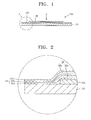
- FIG. 1 is a schematic cross-sectional view of an organic light-emitting display apparatus according to an embodiment of the present invention
- FIG. 2 is a schematic enlarged view of an encapsulation portion of the organic light-emitting display apparatus shown in FIG. 1 ;
- FIG. 3 is a schematic plan view of the organic light-emitting display apparatus shown in FIG. 1 taken from a direction X;
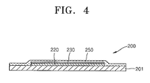
- FIG. 4 is a schematic cross-sectional view of an organic light-emitting display apparatus according to another embodiment of the present invention.
- FIG. 1 is a schematic cross-sectional view of an organic light-emitting display apparatus 100 according to an embodiment of the present invention.
- a display portion 120 which includes an organic light-emitting device (e.g., an organic light-emitting diode) for forming an image, and an encapsulation portion 150, which encapsulates the display portion 120, are formed on a substrate 101.
- a region of the substrate 101 excluding the display potion 120 is referenced as a non-display portion 140 and is shown in FIG. 3 .
- the non-display portion 140 may extend between the edge (or edge portion) of the substrate 101 and the edge (or edge portion) of the display portion 120.
- the edge (or edge portion) of the display portion 120 may be the outer edge of the outermost light emitting diodes or the outer circumference of the outermost light emitting diodes.
- FIG. 2 is a schematic enlarged view of the encapsulation portion 150 of FIG.
- the first encapsulation layer 151 is formed of an inorganic material to block or prevent gas or moisture from penetrating from outside.
- the first encapsulation layer 151 may be formed of a metal nitride and/or oxide containing calcium oxide, alumina, silica, titania, indium oxide, silicon oxide, silicon nitride, and/or aluminum nitride.
- the second encapsulation layer 152 is formed of an organic material to relieve stress from the inside of the first encapsulation layer 151, fill out any possible defects, such as cracks, pinholes, etc., formed in the surface of the first encapsulation layer 151, and make the encapsulation portion 150 to be overall smooth.
- the second encapsulation layer 152 may contain acrylic, meta acrylic, polyester, PET, polyethylene, and/or polypropylene.
- the present invention is not limited thereto. That is, the number of times the first encapsulation layer 151 and the second encapsulation layer 152 are alternately stacked is not limited in the present invention, and two or more pairs of the first encapsulation layer 151 and the second encapsulation layer 152 may be alternately stacked.
- An area of the second encapsulation layer 152 is greater than that of the display portion 120, so as to cover the display portion 120.
- An area of the first encapsulation layer 151 is greater than that of the second encapsulation layer 152, so that the area of the first encapsulation layer 151 is greater than the areas of the display portion 120 and the second encapsulation layer 152.
- the first encapsulation layer 151 and the second encapsulation layer 152 are alternately stacked on the upper portion of the display portion 120. Only the first encapsulation layer 151 is stacked on the peripheral region of the display portion 120. As a result, an end portion of the first encapsulation layer 151 contacts the substrate 101, and only the first encapsulation layer 151 is stacked on the outermost circumference of the encapsulation portion 150 on the peripheral region of the display portion 120. Also, the first, first encapsulation layer 151 a that is the lowest layer of the encapsulation portion 150 contacts the substrate 101 as shown in FIG. 2 .
- an organic layer that is more vulnerable to moisture than an inorganic layer is easily deformed and moisture may be transferred therein.
- the second encapsulation layer 152 and the first encapsulation layer 151 are alternately stacked on the peripheral region of the display portion 120 formed on the substrate 101, moisture more easily penetrates into the display portion 120 through the second encapsulation layer 152 than the first encapsulation layer 151.
- an end region of the encapsulation portion 150 that is the outermost circumference of the substrate 101 does not include the second encapsulation layer 152 on the peripheral region of the display portion 120 in the encapsulation structure of the present embodiment.
- the organic light-emitting display apparatus 100 effectively prevents a defect caused by contaminates, such as moisture, dust, or gas that may penetrate into the side surface of the display portion 120, in particular, a defect that occurs on the edge of the display portion 120, thereby improving the image quality properties of the organic light-emitting display apparatus 100.
- the thickness of the second encapsulation layer 152 is greater than that of the first encapsulation layer 151.
- the first encapsulation layer 151 may be formed by using sputtering, chemical vapor deposition (CVD), ion beam assisted deposition (IBAD), etc.
- the first encapsulation layer 151 that is formed to be too thick may have too many defects that occur and may increase the manufacturing process and cost due to a slow filming operation.
- the first encapsulation layer 151 is formed as a thin film (or multiple thin films).
- the second encapsulation layer 152 containing an organic material is formed by depositing liquefied or gasified monomer and curing the deposited monomer by irradiating UV.
- the second encapsulation layer 152 having a greater thickness than the first encapsulation layer 151 can be more easily manufactured than the first encapsulation layer 151, and may have a uniform thickness and elaborate structure.
- the second encapsulation layer 152 having a greater thickness than the first encapsulation layer 151 can flatten the encapsulation portion 150 formed on the upper portion of the display portion 120 so that the encapsulation portion 150 has an overall elaborate structure and protects the display portion 120 from contamination of outside air and/or penetration of moisture. Also, on the regions corresponding to the upper and side portions of the display portion 120 shown in FIG. 2 , the thickness of the second encapsulation layer 152 is greater than that of the first encapsulation layer 151.
- FIG. 4 is a schematic cross-sectional view of an organic light-emitting display apparatus 200 according to another embodiment of the present invention.
- a display portion 220 is formed on a substrate 201.
- An encapsulation portion 250 is formed on the substrate 201 to encapsulate the display portion 220.
- a light function layer 230 is disposed between the display portion 220 and the encapsulation portion 250.
- the substrate 201, the display portion 220, and the encapsulation portion 250 are the same (or substantially the same) as described in the previous embodiment and thus their detailed descriptions are not provided again.
- the light function layer 230 is disposed between the display portion 220 and the encapsulation portion 250, thereby preventing damage to a portion (or a lower portion) of an organic light-emitting device due to the irradiated UV (or protecting this portion of the organic light-emitting device from damage caused by the irradiated UV).
- the light function layer 230 is formed of a material that reflects UV and increases a light extraction efficiency of the display portion 220.
- the light function layer 230 is formed of AIq3, benzophenone, photo acryl, BaF 2 , CsF, Na 5 Al 3 F 14 , KCl, and/or SiO, and, in particular, may be formed of AIq3.
- the light function layer 230 is shown as a single layer in the present embodiment, the present invention is not limited thereto. That is, the light function layer 230 may be a multilayer structure. In this regard, if each layer of the light function layer 230 is formed of a material having a different refraction index, the reflection of UV increases. When the light function layer 230 is the multilayer and if the thickness of each layer is 1/4 the wavelength of UV, the light function layer 230 increases the reflection of UV.
- the light function layer 230 resonates light generated by the display portion 220, thereby increasing the light extraction efficiency of the display portion 220.
- the thickness of the light function layer 230 is between about 20 nm and about 200 nm in order to increase the light extraction efficiency and the color purity of the display portion 220.
- the thickness of the light function layer 230 is less than 20 nm, the light function layer 230 may be vulnerable to the penetration of UV, which deteriorates device properties. In one embodiment of the present invention, the thickness of the light function layer 230 is more than 50 nm. Because the light extraction efficiency and the color purity of the display portion 220 may be reduced if the thickness of the light function layer 230 exceeds 200 nm, the thickness of the light function layer 230 is less than 200 nm in another embodiment of the present invention. In one embodiment of the present invention, the thickness of the light function layer 230 is less than 150 nm.
- an organic light-emitting display apparatus can easily encapsulate an organic light-emitting device and improve its electrical properties.
Landscapes
- Chemical & Material Sciences (AREA)
- Inorganic Chemistry (AREA)
- Physics & Mathematics (AREA)
- Optics & Photonics (AREA)
- Electroluminescent Light Sources (AREA)
- Devices For Indicating Variable Information By Combining Individual Elements (AREA)
Abstract
Description
- This application claims priority to and the benefit of Korean Patent Application No.
10-2009-0004572, filed on January 20, 2009 - The present invention relates to an organic light-emitting display apparatus, and, more particularly, to an organic light-emitting display apparatus for encapsulating an organic light-emitting device.
- Organic and inorganic light-emitting display apparatuses are flat panel display apparatuses. In addition, organic and inorganic light-emitting display apparatuses are self-emitting display apparatuses that have wide viewing angle, good contrast, and rapid response speed. In addition, organic light-emitting display apparatuses including a light-emitting layer formed of an organic material have better brightness, lower driving voltage, and higher response speed characteristics than inorganic light-emitting display apparatuses, and can provide multicolored images. However, organic light-emitting display apparatuses can easily deteriorate due to contamination from outside air and penetration of moisture. In order to protect the organic light-emitting devices (e.g., the organic light-emitting diodes) of the organic light-emitting display apparatuses from the deterioration caused by the contamination of outside air and/or penetration of moisture, a thin film encapsulation method of alternately stacking organic layers and inorganic layers has been developed. The thin film encapsulation method can be used on an organic light-emitting display apparatus having a large, flexible, bendable, and/or ultra-thin film display.
- With reference to a region horizontal to an upper portion of an organic light-emitting device (e.g., an organic light-emitting diode) included in an encapsulation layer region of an alternately stacked structure, impurities, air, or moisture may easily penetrate into the peripheral region of the organic light-emitting device.
- Also, during a process of depositing organic layers, an organic light-emitting device is exposed to ultraviolet (UV) rays when liquefied or gasified organic monomer is cured by irradiating UV to form polymer, which deteriorates the properties of the organic layers included in the organic light-emitting device, and changes the interface properties between the organic layers and electrodes included in the organic light-emitting device. Thus, the electrical properties of the organic light-emitting device may be deteriorated and/or a leakage current may occur when a voltage is applied to the organic light-emitting device, thereby increasing power consumption of the organic light-emitting display apparatus that includes the organic light-emitting device and reducing the lifespan thereof.
- An aspect of an embodiment of the present invention is directed toward an organic light-emitting display apparatus for protecting an organic light-emitting device (e.g., an organic light-emitting diode) from external impurities, such as gas and moisture, and/or improving the electrical properties of the organic light-emitting device.
- According to an embodiment of the present invention, there is provided an organic light-emitting display apparatus including: a substrate; a display portion on the substrate and including an organic light-emitting device (preferably a plurality of organic light-emitting diodes which are arranged in a matrix); a non-display portion being a peripheral region of the display portion on the substrate; and an encapsulation layer on the display portion (preferably on the organic light-emitting device) and including at least a first encapsulation layer composed of an inorganic material and at least a second encapsulation layer composed of an organic material, the first and second encapsulation layers being alternately stacked on the display portion (preferably on the organic light-emitting device), wherein at least a portion of an end portion of the encapsulation layer which contacts the non-display portion of the substrate, includes only the first encapsulation layer.
- Preferably the complete circumference of the (outmost) end portion of the encapsulation layer, which contacts the non-display portion of the substrate, comprises only the first encapsulation layer. That is, the first and second encapsulation layers are alternately stacked in the display portion but the first and second encapsulation layers are not alternately stacked in the portion of the outer circumference of the first encapsulation layer. That is, the stacked structure of the encapsulation layer extends over the display portion and in an area of the non-display portion which is adjacent to the display portion, the stacked structure of the encapsulation layer transforms into a structure of only the first encapsulation layer so that in a more outmost region of the encapsulation layer (of the non-display portion) the lateral end portions of the encapsulation layer is only formed of the first encapsulation layer. Accordingly, the second encapsulation layer is not present in the lateral end portions of the encapsulation layer.
- Preferably, the second encapsulation layer narrows in a region which is adjacent to the edge of the organic light-emitting device, i.e. a region which is located directly adjacent to the outer circumference of a projection of the organic light-emitting device onto the (second) encapsulation layer along an axis being perpendicular to the substrate. That is, the at least one second encapsulation layer comprises a tapered portion in said region. This tapered portion forms a step in the region where the encapsulation layer contacts the edge of the organic light-emitting device which can more efficiently avoid cracking in said stepped region.
- An area of the second encapsulation layer may be greater than that of the display portion. Preferably, a respective area of all second encapsulation layers may be greater than the area of the display portion. Accordingly, the second encapsulation layer completely covers the display portion. In more particular, a projection of the second encapsulation layer along a first axis onto the display portion completely covers the display portion, wherein the first axis is parallel to the normal vector of the upper surface of the substrate. Preferably, the upper surface of the substrate is a completely planar surface. More preferably, the upper surface of the substrate is a completely planar surface in the area of the display portion.
- The thickness of the second encapsulation layer may be greater than that of the first encapsulation layer. Preferably the respective thickness of all second encapsulation layers may be greater than the thickness of the thickest first encapsulation layer. Preferably, the first encapsulation layer and/or the second encapsulation layer comprise a uniform thickness in the display portion. Preferably, the number of first encapsulation layers and the number of second encapsulation layers is equal to each other. Alternatively, one more first encapsulation layers is provided compared to the number of second encapsulation layers (the lowest and the uppermost layer are then first encapsulation layers and the second encapsulation layers are stacked therebetween). Preferably, the number of first encapsulation layers and the number of second encapsulation layers ranges between 2 and 20. More preferably, the number of first encapsulation layers and the number of second encapsulation layers ranges between 2 and 6. Preferably, all first encapsulation layers have the same thickness. Preferably, all second encapsulation layers have the same thickness.
- An area of the first encapsulation layer may be greater than that of the second encapsulation layer. Preferably, a respective area of all first encapsulation layers may be greater the respective largest area of the second encapsulation layers. Accordingly, the first encapsulation layer (at least one first encapsulation layer) completely covers the second encapsulation layer (at least one second encapsulation layer). In more particular, a projection of the first encapsulation layer along the first axis onto the second encapsulation layer completely covers the encapsulation layer.
- The first encapsulation layer may include a lowest layer of the encapsulation portion that is closest to the display portion.
- The second encapsulation layer may include a lowest layer of the encapsulation portion that is closest to the display portion.
- The organic light-emitting display apparatus may further include: a light function layer disposed between the display portion and the encapsulation portion. The light function layer is preferably adapted to reflect UV (ultraviolet light) and to increase the light extraction efficiency of the display portion. In the sense of the present invention, ultraviolet light is radiation having a wavelength between 150 nm and 380 nm, more preferably between 200 nm and 380. Preferably, the light function layer has a reflectance for ultraviolet light of more than 0.2, more preferably of more than 0.4, more preferably of more than 0.6, more preferably of more than 0.8 and still more preferably of more than 0.9. Preferably, the light function layer has a reflectance for visible light (380 nm - 780 nm) emitted by the organic light-emitting device of less than 0.6, more preferably of less than 0.4, more preferably of less than 0.2 and still more preferably of less than 0.1.
- The light function layer may be formed of a material selected from the group consisting of AIq3, benzophenone, photo acryl, BaF2, CsF, Na5Al3F14, KCI, SiO, and combinations thereof.
- The thickness of the light function layer may be between about 20 nm and about 200 nm. More preferably, the thickness of the light function layer ranges between 100 nm and 150nm, more preferably, the thickness of the light function layer ranges between 110 nm and 140nm and still more preferably, the thickness of the light function layer ranges between 120 nm and 130nm. Preferably, the light function layer has a uniform thickness. Preferably, the light function layer has a uniform thickness at least in an area of the display portion.
- At least one of the first encapsulation layer or the second encapsulation layer of the encapsulation portion (encapsulation layer) may have a flat surface at a position corresponding to the display portion. Preferably, all first encapsulation layers and/or all second encapsulation layers have a flat surface at a position corresponding to the display portion. In the sense of the present invention, a flat surface means a planar surface having a maximum curvature (on the upper side) of less than 1/R, wherein R is the radius of curvature and preferably R is greater than 0.1m, more preferably R is greater than 1 m, more preferably R is greater than 10m, more preferably R is greater than 100m and still more preferably R is greater than 1 km.
- The encapsulation portion (=encapsulation layer) may have a flat surface at a position corresponding to the display portion.
- Preferably the first encapsulation layer comprises a first, first encapsulation layer on the display portion, wherein the second encapsulation layer comprises a first, second encapsulation layer on the first, first encapsulation layer, and wherein the first encapsulation further comprises a second, first encapsulation layer on the first, second encapsulation layer.
- Preferably the second encapsulation layer further comprises a second, second encapsulation layer on the second, first encapsulation layer, and wherein the first encapsulation layer further comprises a third, first encapsulation layer on the second, second encapsulation layer.
- Preferably each of the first, first encapsulation layer, the second, first encapsulation layer, and the third, first encapsulation layer is on an outermost perimeter of the substrate.
- According to an embodiment of the present invention, there is provided an organic light-emitting display apparatus comprising: a substrate; a display portion on the substrate and comprising an organic light-emitting device; a non-display portion being a peripheral region of the display portion on the substrate; and an encapsulation layer on the display portion and comprising a first, first encapsulation layer on the display portion, a first, second encapsulation layer on the first, first encapsulation layer, and a second, first encapsulation layer on the first, second encapsulation layer, wherein an end portion of the first, first encapsulation layer contacts the substrate and an end portion of the second, first encapsulation layer contacts the end portion of the first, first encapsulation layer, and wherein each of the first, first encapsulation layer and the second, first encapsulation layer is composed of an inorganic material and the first, second encapsulation layer is composed of an organic material.
- Preferably each of the first, first encapsulation layer and the second, first encapsulation layer is on an outermost perimeter of the substrate.
- Preferably the organic light-emitting display apparatus further comprises: a light function layer between the display portion and the encapsulation portion.
- According to an embodiment of the present invention, there is provided a method for manufacturing an organic light-emitting display apparatus as described above. In this method, the second encapsulation layer is formed by depositing liquefied or gasified monomer and curing the deposited monomer by irradiating UV, and the light function layer is disposed between the display portion and the encapsulation portion, thereby preventing damage to a portion (or a lower portion) of an organic light-emitting device due to the irradiated UV (or protecting this portion of the organic light-emitting device from damage caused by the irradiated UV).
- The light function layer may be a single layer, but the present invention is not limited thereto. That is, the light function layer may be a multilayer structure, the number of layers preferably ranging between 2 and 10. In this regard, preferably each layer of the light function layer is formed of a material having a different refraction index, and accordingly the reflection of UV increases. Preferably, the light function layer is a multilayer and the thickness of each layer is 1/4 the wavelength of UV selected from 200 nm and 380 nm. Advantageously, the light function layer increases the reflection of UV. The light function layer preferably resonates light generated by the display portion, thereby increasing the light extraction efficiency of the display portion. The thickness of each layer may be between about 20 nm and about 200 nm. More preferably, the thickness of each layer ranges between 100 nm and 150nm, more preferably, the thickness of each layer ranges between 110 nm and 140nm and still more preferably, the thickness of each layer ranges between 120 nm and 130nm. Preferably, each layer has a uniform thickness. Preferably, each layer has a uniform thickness at least in an area of the display portion.
- The accompanying drawings, together with the specification, illustrate exemplary embodiments of the present invention, and, together with the description, serve to explain the principles of the present invention.
-
FIG. 1 is a schematic cross-sectional view of an organic light-emitting display apparatus according to an embodiment of the present invention; -
FIG. 2 is a schematic enlarged view of an encapsulation portion of the organic light-emitting display apparatus shown inFIG. 1 ; -
FIG. 3 is a schematic plan view of the organic light-emitting display apparatus shown inFIG. 1 taken from a direction X; and -
FIG. 4 is a schematic cross-sectional view of an organic light-emitting display apparatus according to another embodiment of the present invention. - In the following detailed description, only certain exemplary embodiments of the present invention are shown and described, by way of illustration. As those skilled in the art would recognize, the invention may be embodied in many different forms and should not be construed as being limited to the embodiments set forth herein. Also, in the context of the present application, when an element is referred to as being "on" another element, it can be directly on the other element or be indirectly on the other element with one or more intervening elements interposed therebetween. Like reference numerals designate like elements throughout the specification.
-
FIG. 1 is a schematic cross-sectional view of an organic light-emittingdisplay apparatus 100 according to an embodiment of the present invention. - Referring to
FIG. 1 , adisplay portion 120, which includes an organic light-emitting device (e.g., an organic light-emitting diode) for forming an image, and anencapsulation portion 150, which encapsulates thedisplay portion 120, are formed on asubstrate 101. A region of thesubstrate 101 excluding thedisplay potion 120 is referenced as anon-display portion 140 and is shown inFIG. 3 . Thenon-display portion 140 may extend between the edge (or edge portion) of thesubstrate 101 and the edge (or edge portion) of thedisplay portion 120. The edge (or edge portion) of thedisplay portion 120 may be the outer edge of the outermost light emitting diodes or the outer circumference of the outermost light emitting diodes. -
FIG. 2 is a schematic enlarged view of theencapsulation portion 150 of FIG. - 1. Here, the
encapsulation portion 150 is shown to include afirst encapsulation layer 151 composed of three first encapsulation layers 151 a, 151b, and 151c and asecond encapsulation layer 152 composed of twosecond encapsulation layers display portion 120 and then a first,second encapsulation layer 152a is formed on the first, first encapsulation layer 151 a. A second, first encapsulation layer 151 b; a second,second encapsulation layer 152b; and a third,first encapsulation layer 151c are sequentially formed on the first,second encapsulation layer 152a. However, the present invention is not limited to the above method of forming the encapsulation layers. For example, the second encapsulation layer may be formed on the display portion before the first encapsulation layer is formed on the display portion. That is, either thefirst encapsulation layer 151 or thesecond encapsulation layer 152 may be the lowest layer of theencapsulation portion 150 that is closest to thedisplay portion 120. - The
first encapsulation layer 151 is formed of an inorganic material to block or prevent gas or moisture from penetrating from outside. In more detail, thefirst encapsulation layer 151 may be formed of a metal nitride and/or oxide containing calcium oxide, alumina, silica, titania, indium oxide, silicon oxide, silicon nitride, and/or aluminum nitride. Thesecond encapsulation layer 152 is formed of an organic material to relieve stress from the inside of thefirst encapsulation layer 151, fill out any possible defects, such as cracks, pinholes, etc., formed in the surface of thefirst encapsulation layer 151, and make theencapsulation portion 150 to be overall smooth. Thesecond encapsulation layer 152 may contain acrylic, meta acrylic, polyester, PET, polyethylene, and/or polypropylene. - Although two pairs of the
first encapsulation layer 151 and thesecond encapsulation layer 152 are alternately stacked inFIG. 2 , the present invention is not limited thereto. That is, the number of times thefirst encapsulation layer 151 and thesecond encapsulation layer 152 are alternately stacked is not limited in the present invention, and two or more pairs of thefirst encapsulation layer 151 and thesecond encapsulation layer 152 may be alternately stacked. - An area of the
second encapsulation layer 152 is greater than that of thedisplay portion 120, so as to cover thedisplay portion 120. An area of thefirst encapsulation layer 151 is greater than that of thesecond encapsulation layer 152, so that the area of thefirst encapsulation layer 151 is greater than the areas of thedisplay portion 120 and thesecond encapsulation layer 152. - The
first encapsulation layer 151 and thesecond encapsulation layer 152 are alternately stacked on the upper portion of thedisplay portion 120. Only thefirst encapsulation layer 151 is stacked on the peripheral region of thedisplay portion 120. As a result, an end portion of thefirst encapsulation layer 151 contacts thesubstrate 101, and only thefirst encapsulation layer 151 is stacked on the outermost circumference of theencapsulation portion 150 on the peripheral region of thedisplay portion 120. Also, the first, first encapsulation layer 151 a that is the lowest layer of theencapsulation portion 150 contacts thesubstrate 101 as shown inFIG. 2 . - In general, an organic layer that is more vulnerable to moisture than an inorganic layer is easily deformed and moisture may be transferred therein. Thus, if the
second encapsulation layer 152 and thefirst encapsulation layer 151 are alternately stacked on the peripheral region of thedisplay portion 120 formed on thesubstrate 101, moisture more easily penetrates into thedisplay portion 120 through thesecond encapsulation layer 152 than thefirst encapsulation layer 151. To protect from such penetration, an end region of theencapsulation portion 150 that is the outermost circumference of thesubstrate 101 does not include thesecond encapsulation layer 152 on the peripheral region of thedisplay portion 120 in the encapsulation structure of the present embodiment. - Therefore, the organic light-emitting
display apparatus 100 effectively prevents a defect caused by contaminates, such as moisture, dust, or gas that may penetrate into the side surface of thedisplay portion 120, in particular, a defect that occurs on the edge of thedisplay portion 120, thereby improving the image quality properties of the organic light-emittingdisplay apparatus 100. - In one embodiment, the thickness of the
second encapsulation layer 152 is greater than that of thefirst encapsulation layer 151. Thefirst encapsulation layer 151 may be formed by using sputtering, chemical vapor deposition (CVD), ion beam assisted deposition (IBAD), etc. Thefirst encapsulation layer 151 that is formed to be too thick may have too many defects that occur and may increase the manufacturing process and cost due to a slow filming operation. Thus, in one embodiment of the present invention, thefirst encapsulation layer 151 is formed as a thin film (or multiple thin films). Also, thesecond encapsulation layer 152 containing an organic material is formed by depositing liquefied or gasified monomer and curing the deposited monomer by irradiating UV. Thus, thesecond encapsulation layer 152 having a greater thickness than thefirst encapsulation layer 151 can be more easily manufactured than thefirst encapsulation layer 151, and may have a uniform thickness and elaborate structure. - The
second encapsulation layer 152 having a greater thickness than thefirst encapsulation layer 151 can flatten theencapsulation portion 150 formed on the upper portion of thedisplay portion 120 so that theencapsulation portion 150 has an overall elaborate structure and protects thedisplay portion 120 from contamination of outside air and/or penetration of moisture. Also, on the regions corresponding to the upper and side portions of thedisplay portion 120 shown inFIG. 2 , the thickness of thesecond encapsulation layer 152 is greater than that of thefirst encapsulation layer 151. -
FIG. 4 is a schematic cross-sectional view of an organic light-emittingdisplay apparatus 200 according to another embodiment of the present invention. Referring toFIG. 4 , adisplay portion 220 is formed on asubstrate 201. Anencapsulation portion 250 is formed on thesubstrate 201 to encapsulate thedisplay portion 220. Alight function layer 230 is disposed between thedisplay portion 220 and theencapsulation portion 250. For purposes of convenience of description, differences between the present embodiment and the previous embodiment will now be described. Thesubstrate 201, thedisplay portion 220, and theencapsulation portion 250 are the same (or substantially the same) as described in the previous embodiment and thus their detailed descriptions are not provided again. - Since a second encapsulation layer is formed by depositing liquefied or gasified monomer and curing the deposited monomer by irradiating UV, the
light function layer 230 is disposed between thedisplay portion 220 and theencapsulation portion 250, thereby preventing damage to a portion (or a lower portion) of an organic light-emitting device due to the irradiated UV (or protecting this portion of the organic light-emitting device from damage caused by the irradiated UV). - The
light function layer 230 is formed of a material that reflects UV and increases a light extraction efficiency of thedisplay portion 220. In more detail, thelight function layer 230 is formed of AIq3, benzophenone, photo acryl, BaF2, CsF, Na5Al3F14, KCl, and/or SiO, and, in particular, may be formed of AIq3. - Although the
light function layer 230 is shown as a single layer in the present embodiment, the present invention is not limited thereto. That is, thelight function layer 230 may be a multilayer structure. In this regard, if each layer of thelight function layer 230 is formed of a material having a different refraction index, the reflection of UV increases. When thelight function layer 230 is the multilayer and if the thickness of each layer is 1/4 the wavelength of UV, thelight function layer 230 increases the reflection of UV. Thelight function layer 230 resonates light generated by thedisplay portion 220, thereby increasing the light extraction efficiency of thedisplay portion 220. The thickness of thelight function layer 230 is between about 20 nm and about 200 nm in order to increase the light extraction efficiency and the color purity of thedisplay portion 220. If the thickness of thelight function layer 230 is less than 20 nm, thelight function layer 230 may be vulnerable to the penetration of UV, which deteriorates device properties. In one embodiment of the present invention, the thickness of thelight function layer 230 is more than 50 nm. Because the light extraction efficiency and the color purity of thedisplay portion 220 may be reduced if the thickness of thelight function layer 230 exceeds 200 nm, the thickness of thelight function layer 230 is less than 200 nm in another embodiment of the present invention. In one embodiment of the present invention, the thickness of thelight function layer 230 is less than 150 nm. - In view of the foregoing and according to an embodiment of the present invention, an organic light-emitting display apparatus can easily encapsulate an organic light-emitting device and improve its electrical properties.
- While the present invention has been described in connection with certain exemplary embodiments, it is to be understood that the invention is not limited to the disclosed embodiments, but, on the contrary, is intended to cover various modifications and equivalent arrangements included within the scope of the appended claims, and equivalents thereof.
Claims (15)
- An organic light-emitting display apparatus comprising:a substrate (101, 201);a display portion (120, 220) located on the substrate (101, 201),an organic light-emitting device arranged in the display portion (120, 220);a non-display portion (140) being a peripheral region of the display portion (120, 220) located on the substrate (101, 201); andan encapsulation layer (150, 250) formed on the display portion (120, 220) and comprising at least a first encapsulation layer (151) composed of an inorganic material and at least a second encapsulation layer (152) composed of an organic material, the first and second encapsulation layers (151, 152) being alternately stacked on the display portion (120, 220),
characterized in thatat least a portion of an end portion of the encapsulation layer (150, 250), which contacts the non-display portion (140) of the substrate (101, 201), comprises only the first encapsulation layer (151). - The organic light-emitting display apparatus of claim 1, wherein a surface area of the second encapsulation layer (152) is greater than a surface area of the display portion (120, 220).
- The organic light-emitting display apparatus according to any one of the preceding claims, wherein a thickness of the second encapsulation layer (152) is greater than a thickness of the first encapsulation layer (151).
- The organic light-emitting display apparatus according to any one of the preceding claims, wherein a surface area of the first encapsulation layer (151) is greater than a surface area of the second encapsulation layer (152).
- The organic light-emitting display apparatus according to any one of the preceding claims, wherein the first encapsulation layer (152) comprises a lowest layer of the encapsulation layer (150) closest to the display portion (120, 220) or wherein the second encapsulation layer (152) comprises a lowest layer of the encapsulation layer (150) that is closest to the display portion (120, 220).
- The organic light-emitting display apparatus according to any one of the preceding claims, wherein the first encapsulation layer (151) is formed of a material selected from the group consisting of metal nitride, metal oxide, calcium oxide, alumina, silica, titania, indium oxide, silicon oxide, silicon nitride, aluminum nitride and combinations thereof; and/or the second encapsulation layer (152) comprises one material selected the group consisting of from acrylic, meta acrylic, polyester, PET, polyethylene, polypropylene and combinations thereof.
- The organic light-emitting display apparatus according to any one of the preceding claims, further comprising a light function layer (230) arranged between the display portion (120, 220) and the encapsulation layer (250), the light function layer (230) being adapted to reflect ultraviolet light.
- The organic light-emitting display apparatus of claim 7, wherein the light function layer (230) comprises a material selected from the group consisting of Afq3, benzophenone, photo acryl, BaF2, CsF, Na5Al3F14, KCI, SiO, and combinations thereof.
- The organic light-emitting display apparatus according to any of claims 7 and 8, wherein the light function layer (230) is a single layer with a thickness between from 20 nm and 200 nm.
- The organic light-emitting display apparatus according to any of claims 7 and 8, wherein the light function layer (230) is a multilayer structure, wherein each layer of the multilayer structure of the light function layer (230) has a thickness between from 20 nm and 200 nm and wherein the each layer of the multilayer structure of the light function layer (230) is formed of a material having a different refraction index.
- The organic light-emitting display apparatus according to any one of the preceding claims, wherein at least one of the first encapsulation layer (151) and the second encapsulation layer (152) has a flat surface at a position corresponding to the display portion (120).
- The organic light-emitting display apparatus according to any one of the preceding claims, wherein the encapsulation layer (150, 250) has a flat surface at a position corresponding to the display portion (120, 250).
- The organic light-emitting display apparatus according to any one of the preceding claims, wherein the first encapsulation layer (151) comprises two layers (151a, 151b) arranged on the organic light-emitting device, wherein the second encapsulation layer (152) comprises one layer (152a) interposed between the two layers (151 a, 151 b) of the first encapsulation layer (151).
- The organic light-emitting display apparatus of claim 13, wherein the second encapsulation layer (152) comprises two layers (152a, 152b) and the first encapsulation layer (151) comprises three layers (151a, 151b, 151c) arranged on the display portion (120, 220), respectively, and wherein the two layers (152a, 152b) of the second encapsulation layer (152) are interposed between the outermost of the three layers (151a, 151b, 151c) of the first encapsulation layer (151), and wherein the layers (151a, 152a, 151b, 152b, 151c) of the first and second encapsulation layers (151, 152) are alternately stacked on each other.
- The organic light-emitting display apparatus of claim 14, wherein each of the three layers (151a, 151b, 151c) of the first encapsulation layer (151) laterally terminates on the edge of the outermost perimeter of the substrate (101).
Applications Claiming Priority (1)
| Application Number | Priority Date | Filing Date | Title |
|---|---|---|---|
| KR1020090004572A KR101001552B1 (en) | 2009-01-20 | 2009-01-20 | Organic light emitting display |
Publications (1)
| Publication Number | Publication Date |
|---|---|
| EP2209149A1 true EP2209149A1 (en) | 2010-07-21 |
Family
ID=42060544
Family Applications (1)
| Application Number | Title | Priority Date | Filing Date |
|---|---|---|---|
| EP10150999A Ceased EP2209149A1 (en) | 2009-01-20 | 2010-01-18 | Organic light emitting display apparatus |
Country Status (6)
| Country | Link |
|---|---|
| US (1) | US8552634B2 (en) |
| EP (1) | EP2209149A1 (en) |
| JP (2) | JP2010171012A (en) |
| KR (1) | KR101001552B1 (en) |
| CN (1) | CN101794810B (en) |
| TW (1) | TWI454173B (en) |
Cited By (5)
| Publication number | Priority date | Publication date | Assignee | Title |
|---|---|---|---|---|
| EP2581958A3 (en) * | 2011-10-14 | 2015-07-15 | Samsung Display Co., Ltd. | Organic light emitting diode display and method for manufacturing the same |
| KR20170140802A (en) * | 2017-12-11 | 2017-12-21 | 삼성디스플레이 주식회사 | Organic light emitting diode display and method for manufacturing the same |
| US9853245B2 (en) | 2011-10-14 | 2017-12-26 | Samsung Display Co., Ltd. | Organic light emitting diode display and method for manufacturing the same |
| KR20190007514A (en) * | 2019-01-14 | 2019-01-22 | 삼성디스플레이 주식회사 | Organic light emitting diode display and method for manufacturing the same |
| CN111128010A (en) * | 2018-11-01 | 2020-05-08 | 京东方科技集团股份有限公司 | Display panel, manufacturing method thereof and display device |
Families Citing this family (47)
| Publication number | Priority date | Publication date | Assignee | Title |
|---|---|---|---|---|
| KR101430173B1 (en) * | 2010-10-19 | 2014-08-13 | 삼성디스플레이 주식회사 | Organic light emitting diode display |
| US20120235304A1 (en) * | 2011-03-18 | 2012-09-20 | Globalfoundries Inc. | Ultraviolet (uv)-reflecting film for beol processing |
| KR101863853B1 (en) * | 2011-07-29 | 2018-06-04 | 삼성디스플레이 주식회사 | Organic light emitting diode display and method for manufacturing the same |
| JPWO2013111218A1 (en) * | 2012-01-23 | 2015-05-11 | 株式会社アルバック | Element structure and method for manufacturing element structure |
| KR101931174B1 (en) | 2012-03-22 | 2019-03-14 | 삼성디스플레이 주식회사 | Organic light emitting display device and manufacturing method thereof |
| KR102048926B1 (en) * | 2012-11-19 | 2019-11-27 | 삼성디스플레이 주식회사 | Organic light emitting display apparatus and the manufacturing method thereof |
| KR101502206B1 (en) | 2012-11-20 | 2015-03-12 | 삼성디스플레이 주식회사 | Organic light emitting display device having improved light emitting efficiency |
| US9349988B2 (en) | 2012-11-20 | 2016-05-24 | Samsung Display Co., Ltd. | Organic light emitting display device |
| KR101410102B1 (en) | 2012-11-20 | 2014-06-27 | 삼성디스플레이 주식회사 | Organic light emitting display device |
| US9692010B2 (en) | 2012-11-20 | 2017-06-27 | Samsung Display Co., Ltd. | Organic light emitting display device |
| KR102066079B1 (en) * | 2012-12-27 | 2020-01-14 | 엘지디스플레이 주식회사 | Organic light emitting diode display device and method of manufacturing the same |
| KR102047922B1 (en) * | 2013-02-07 | 2019-11-25 | 삼성디스플레이 주식회사 | Flexible substrate, method for manufacturing flexible substrate, flexible display device, and method for flexible display device |
| US9331311B2 (en) * | 2013-03-04 | 2016-05-03 | Applied Materials, Inc. | Fluorine-containing plasma polymerized HMDSO for OLED thin film encapsulation |
| KR102052075B1 (en) | 2013-03-28 | 2020-01-09 | 삼성디스플레이 주식회사 | Deposition apparatus, method for forming thin film using the same, organic light emitting display apparatus and method for manufacturing the same |
| KR102133433B1 (en) * | 2013-05-24 | 2020-07-14 | 삼성디스플레이 주식회사 | TFT substrate including barrier layer including silicon oxide layer and silicon silicon nitride layer, Organic light-emitting device comprising the TFT substrate, and the manufacturing method of the TFT substrate |
| KR20150011231A (en) * | 2013-07-22 | 2015-01-30 | 삼성디스플레이 주식회사 | Organic light emitting display apparatus and the manufacturing method thereof |
| KR102097031B1 (en) * | 2013-07-22 | 2020-04-06 | 삼성디스플레이 주식회사 | Foldable display and method of manufacturing the same |
| KR102093393B1 (en) * | 2013-08-14 | 2020-03-26 | 삼성디스플레이 주식회사 | Organic light emitting display apparatus and the manufacturing method thereof |
| JP6169439B2 (en) * | 2013-08-21 | 2017-07-26 | 株式会社ジャパンディスプレイ | Organic electroluminescence display device and manufacturing method thereof |
| WO2015029608A1 (en) * | 2013-08-28 | 2015-03-05 | シャープ株式会社 | Electroluminescent device and method for manufacturing same |
| WO2015047044A1 (en) * | 2013-09-30 | 2015-04-02 | 주식회사 엘지화학 | Method for manufacturing organic electronic device |
| KR102165869B1 (en) | 2013-10-21 | 2020-10-15 | 삼성디스플레이 주식회사 | Encapsulating member and display device having the same |
| KR102136790B1 (en) * | 2013-11-15 | 2020-07-23 | 삼성디스플레이 주식회사 | Flexible display device and the fabrication method thereof |
| KR102122359B1 (en) * | 2013-12-10 | 2020-06-12 | 삼성전자주식회사 | Method for manufacturing light emitting device |
| KR102253531B1 (en) | 2014-07-25 | 2021-05-18 | 삼성디스플레이 주식회사 | Display device and method for manufacturing the same |
| KR102250048B1 (en) | 2014-09-16 | 2021-05-11 | 삼성디스플레이 주식회사 | Organic light emitting display device |
| KR102314467B1 (en) * | 2014-10-13 | 2021-10-20 | 삼성디스플레이 주식회사 | Display apparatus and method of manufacturing the same |
| KR102328677B1 (en) * | 2014-10-17 | 2021-11-19 | 삼성디스플레이 주식회사 | Flexible display apparatus and manufacturing method thereof |
| CN104900812A (en) | 2015-04-23 | 2015-09-09 | 京东方科技集团股份有限公司 | Film packaging structure, manufacture method thereof and display device |
| WO2017033440A1 (en) * | 2015-08-21 | 2017-03-02 | シャープ株式会社 | Organic el display device |
| CN105552247B (en) * | 2015-12-08 | 2018-10-26 | 上海天马微电子有限公司 | Composite substrate, flexible display device and preparation method thereof |
| JP2017152256A (en) * | 2016-02-25 | 2017-08-31 | 株式会社ジャパンディスプレイ | Display device |
| US10608205B2 (en) | 2016-03-07 | 2020-03-31 | Pioneer Corporation | Sealing structure and light emitting device |
| CN107565032A (en) * | 2016-06-30 | 2018-01-09 | 张家港保税区冠祥贸易有限公司 | A kind of organic light-emitting display device |
| JP6815159B2 (en) * | 2016-10-14 | 2021-01-20 | 株式会社ジャパンディスプレイ | Display device |
| US10305064B2 (en) | 2017-04-28 | 2019-05-28 | Wuhan China Star Optoelectronics Technology Co., Ltd. | Flexible organic light emitting diode display and manufacturing method thereof |
| CN107195800A (en) * | 2017-04-28 | 2017-09-22 | 武汉华星光电技术有限公司 | A kind of flexible organic light emitting diode display and preparation method thereof |
| CN109509402B (en) * | 2017-09-14 | 2022-03-18 | 广州国显科技有限公司 | Flexible display device |
| US10815566B2 (en) * | 2017-10-19 | 2020-10-27 | Wuhan China Star Optoelectronics Semiconductor Display Technology Co., Ltd. | Flexible substrate and manufacturing method thereof, display |
| CN108054290A (en) * | 2017-12-27 | 2018-05-18 | 深圳市华星光电技术有限公司 | The encapsulating structure and method for packing of OLED display |
| US20190198809A1 (en) * | 2017-12-27 | 2019-06-27 | Wuhan China Star Optoelectronics Semiconductor Display Technology Co., Ltd. | Thin-film encapsulation structure and method for oled |
| JP6515224B2 (en) * | 2018-03-05 | 2019-05-15 | 堺ディスプレイプロダクト株式会社 | Method of manufacturing organic EL device and film forming apparatus |
| US10734607B2 (en) * | 2018-05-23 | 2020-08-04 | Wuhan China Star Optoelectronics Semiconductor Display Technology Co., Ltd. | Organic light emitting diode display panel and method for encapsulating same |
| CN108899438A (en) * | 2018-06-21 | 2018-11-27 | 武汉华星光电半导体显示技术有限公司 | Display panel and preparation method thereof |
| KR102075841B1 (en) * | 2018-08-29 | 2020-02-10 | 고려대학교 세종산학협력단 | Flexible Display and Manufacturing Method thereof |
| KR102814722B1 (en) * | 2019-10-29 | 2025-05-30 | 삼성디스플레이 주식회사 | Display apparatus |
| CN114141968A (en) * | 2021-11-25 | 2022-03-04 | 深圳市华星光电半导体显示技术有限公司 | Display panel, manufacturing method and electronic device |
Citations (5)
| Publication number | Priority date | Publication date | Assignee | Title |
|---|---|---|---|---|
| US20030184219A1 (en) * | 2002-03-29 | 2003-10-02 | General Electric Company | Mechanically flexible organic electroluminescent device with directional light emission |
| US20050239294A1 (en) * | 2002-04-15 | 2005-10-27 | Rosenblum Martin P | Apparatus for depositing a multilayer coating on discrete sheets |
| US20070181872A1 (en) * | 2006-02-03 | 2007-08-09 | Lee Young-Gu | Organic light emitting display and manufacturing method thereof |
| US20080238301A1 (en) * | 2007-03-30 | 2008-10-02 | Samsung Electronics Co., Ltd. | Organic electro luminescence device and method of fabricating the same |
| US20080296600A1 (en) * | 2007-05-30 | 2008-12-04 | Kwack Jin-Ho | Organic light emitting diode (OLED) display and method of manufacturing the same |
Family Cites Families (12)
| Publication number | Priority date | Publication date | Assignee | Title |
|---|---|---|---|---|
| TW411726B (en) * | 1998-06-18 | 2000-11-11 | Siemens Ag | Manufacture of structurized electrodes |
| EP0966050A3 (en) * | 1998-06-18 | 2004-11-17 | Osram Opto Semiconductors GmbH & Co. OHG | Organic light emitting diode |
| US6881447B2 (en) * | 2002-04-04 | 2005-04-19 | Dielectric Systems, Inc. | Chemically and electrically stabilized polymer films |
| DE10132699A1 (en) * | 2001-07-05 | 2003-01-16 | Philips Corp Intellectual Pty | Organic electroluminescent display device with optical filter |
| JP2003151761A (en) * | 2001-11-14 | 2003-05-23 | Osaka Industrial Promotion Organization | Light emitting device including organic EL device and optical interconnection device using the same |
| WO2005105428A1 (en) | 2004-04-28 | 2005-11-10 | Zeon Corporation | Multilayer body, light-emitting device and use thereof |
| JP2006004650A (en) | 2004-06-15 | 2006-01-05 | Toshiba Matsushita Display Technology Co Ltd | Display element and optical device |
| JP4511440B2 (en) * | 2004-10-05 | 2010-07-28 | 三星モバイルディスプレイ株式會社 | ORGANIC LIGHT EMITTING ELEMENT AND METHOD FOR PRODUCING ORGANIC LIGHT EMITTING ELEMENT |
| JP2006278021A (en) | 2005-03-28 | 2006-10-12 | Pioneer Electronic Corp | Inspection method and structure of organic function element sealing film |
| KR100682963B1 (en) * | 2006-02-03 | 2007-02-15 | 삼성전자주식회사 | Organic light emitting display with UV blocking film |
| KR100770127B1 (en) * | 2006-11-10 | 2007-10-24 | 삼성에스디아이 주식회사 | Organic electroluminescent display and manufacturing method thereof |
| JP2008210665A (en) | 2007-02-27 | 2008-09-11 | Canon Inc | ORGANIC LIGHT EMITTING ELEMENT AND DISPLAY DEVICE USING THE SAME |
-
2009
- 2009-01-20 KR KR1020090004572A patent/KR101001552B1/en active Active
-
2010
- 2010-01-08 US US12/684,560 patent/US8552634B2/en active Active
- 2010-01-14 TW TW099100890A patent/TWI454173B/en active
- 2010-01-18 EP EP10150999A patent/EP2209149A1/en not_active Ceased
- 2010-01-19 JP JP2010009315A patent/JP2010171012A/en active Pending
- 2010-01-20 CN CN201010004301.3A patent/CN101794810B/en active Active
-
2012
- 2012-08-07 JP JP2012174714A patent/JP5513565B2/en active Active
Patent Citations (5)
| Publication number | Priority date | Publication date | Assignee | Title |
|---|---|---|---|---|
| US20030184219A1 (en) * | 2002-03-29 | 2003-10-02 | General Electric Company | Mechanically flexible organic electroluminescent device with directional light emission |
| US20050239294A1 (en) * | 2002-04-15 | 2005-10-27 | Rosenblum Martin P | Apparatus for depositing a multilayer coating on discrete sheets |
| US20070181872A1 (en) * | 2006-02-03 | 2007-08-09 | Lee Young-Gu | Organic light emitting display and manufacturing method thereof |
| US20080238301A1 (en) * | 2007-03-30 | 2008-10-02 | Samsung Electronics Co., Ltd. | Organic electro luminescence device and method of fabricating the same |
| US20080296600A1 (en) * | 2007-05-30 | 2008-12-04 | Kwack Jin-Ho | Organic light emitting diode (OLED) display and method of manufacturing the same |
Cited By (11)
| Publication number | Priority date | Publication date | Assignee | Title |
|---|---|---|---|---|
| EP2581958A3 (en) * | 2011-10-14 | 2015-07-15 | Samsung Display Co., Ltd. | Organic light emitting diode display and method for manufacturing the same |
| US9853245B2 (en) | 2011-10-14 | 2017-12-26 | Samsung Display Co., Ltd. | Organic light emitting diode display and method for manufacturing the same |
| US10396312B2 (en) | 2011-10-14 | 2019-08-27 | Samsung Display Co., Ltd. | Organic light emitting diode display and method for manufacturing the same |
| US10854847B2 (en) | 2011-10-14 | 2020-12-01 | Samsung Display Co., Ltd. | Organic light emitting diode display and method for manufacturing the same |
| US11335889B2 (en) | 2011-10-14 | 2022-05-17 | Samsung Display Co., Ltd. | Organic light emitting diode display and method for manufacturing the same |
| US11793028B2 (en) | 2011-10-14 | 2023-10-17 | Samsung Display Co., Ltd. | Organic light emitting diode display and method for manufacturing the same |
| US12289952B2 (en) | 2011-10-14 | 2025-04-29 | Samsung Display Co., Ltd. | Organic light emitting diode display and method for manufacturing the same |
| KR20170140802A (en) * | 2017-12-11 | 2017-12-21 | 삼성디스플레이 주식회사 | Organic light emitting diode display and method for manufacturing the same |
| CN111128010A (en) * | 2018-11-01 | 2020-05-08 | 京东方科技集团股份有限公司 | Display panel, manufacturing method thereof and display device |
| CN111128010B (en) * | 2018-11-01 | 2021-10-29 | 京东方科技集团股份有限公司 | Display panel, method for manufacturing the same, and display device |
| KR20190007514A (en) * | 2019-01-14 | 2019-01-22 | 삼성디스플레이 주식회사 | Organic light emitting diode display and method for manufacturing the same |
Also Published As
| Publication number | Publication date |
|---|---|
| TW201038110A (en) | 2010-10-16 |
| CN101794810A (en) | 2010-08-04 |
| JP2010171012A (en) | 2010-08-05 |
| KR101001552B1 (en) | 2010-12-17 |
| CN101794810B (en) | 2015-02-11 |
| US20100181903A1 (en) | 2010-07-22 |
| JP2012238611A (en) | 2012-12-06 |
| JP5513565B2 (en) | 2014-06-04 |
| KR20100085347A (en) | 2010-07-29 |
| US8552634B2 (en) | 2013-10-08 |
| TWI454173B (en) | 2014-09-21 |
Similar Documents
| Publication | Publication Date | Title |
|---|---|---|
| EP2209149A1 (en) | Organic light emitting display apparatus | |
| US12557381B2 (en) | Display apparatus and method of manufacturing the same | |
| US11616177B2 (en) | Display apparatus and manufacturing method thereof | |
| CN102272974B (en) | Tiled OLED device with edge light extraction | |
| JP6342609B2 (en) | Organic light emitting display device and method for manufacturing organic light emitting display device | |
| EP3190623B1 (en) | Organic light-emitting diode display panel, manufacturing method therefor, and display apparatus | |
| CN102856349B (en) | Display device and image-information processing apparatus equipped with the same | |
| US8981643B2 (en) | Electroluminescent display panel | |
| US8664852B2 (en) | Organic light emitting display device and method for manufacturing the same | |
| US9978821B2 (en) | Display device | |
| CN105390525A (en) | Display device and manufacturing method thereof | |
| JP2009501426A (en) | OLED devices with improved efficiency and durability | |
| CN110970572B (en) | Packaging structure, display panel and display device | |
| US11018321B2 (en) | Sealing structure and light emitting device | |
| CN114093915A (en) | Display panel and display device | |
| US20250057019A1 (en) | Display device and method of manufacturing display device | |
| KR20230022374A (en) | Display apparatus | |
| JP7588951B2 (en) | Organic electroluminescent display device | |
| US12543484B2 (en) | Display device | |
| JP2011150960A (en) | Light emitting device |
Legal Events
| Date | Code | Title | Description |
|---|---|---|---|
| PUAI | Public reference made under article 153(3) epc to a published international application that has entered the european phase |
Free format text: ORIGINAL CODE: 0009012 |
|
| 17P | Request for examination filed |
Effective date: 20100118 |
|
| AK | Designated contracting states |
Kind code of ref document: A1 Designated state(s): AT BE BG CH CY CZ DE DK EE ES FI FR GB GR HR HU IE IS IT LI LT LU LV MC MK MT NL NO PL PT RO SE SI SK SM TR |
|
| AX | Request for extension of the european patent |
Extension state: AL BA RS |
|
| 17Q | First examination report despatched |
Effective date: 20110517 |
|
| APBK | Appeal reference recorded |
Free format text: ORIGINAL CODE: EPIDOSNREFNE |
|
| APBN | Date of receipt of notice of appeal recorded |
Free format text: ORIGINAL CODE: EPIDOSNNOA2E |
|
| APBR | Date of receipt of statement of grounds of appeal recorded |
Free format text: ORIGINAL CODE: EPIDOSNNOA3E |
|
| RAP1 | Party data changed (applicant data changed or rights of an application transferred) |
Owner name: SAMSUNG DISPLAY CO., LTD. |
|
| APAF | Appeal reference modified |
Free format text: ORIGINAL CODE: EPIDOSCREFNE |
|
| RAP1 | Party data changed (applicant data changed or rights of an application transferred) |
Owner name: SAMSUNG DISPLAY CO., LTD. |
|
| APBT | Appeal procedure closed |
Free format text: ORIGINAL CODE: EPIDOSNNOA9E |
|
| STAA | Information on the status of an ep patent application or granted ep patent |
Free format text: STATUS: THE APPLICATION HAS BEEN REFUSED |
|
| 18R | Application refused |
Effective date: 20180309 |