EP2209142B1 - Semiconductor device and manufacturing method thereof - Google Patents
Semiconductor device and manufacturing method thereof Download PDFInfo
- Publication number
- EP2209142B1 EP2209142B1 EP08847499.4A EP08847499A EP2209142B1 EP 2209142 B1 EP2209142 B1 EP 2209142B1 EP 08847499 A EP08847499 A EP 08847499A EP 2209142 B1 EP2209142 B1 EP 2209142B1
- Authority
- EP
- European Patent Office
- Prior art keywords
- electrode
- semiconductor
- insulation film
- interlayer insulation
- region
- Prior art date
- Legal status (The legal status is an assumption and is not a legal conclusion. Google has not performed a legal analysis and makes no representation as to the accuracy of the status listed.)
- Active
Links
- 239000004065 semiconductor Substances 0.000 title claims description 357
- 238000004519 manufacturing process Methods 0.000 title description 46
- 238000009413 insulation Methods 0.000 claims description 166
- 239000011229 interlayer Substances 0.000 claims description 143
- 239000000758 substrate Substances 0.000 claims description 33
- 238000000034 method Methods 0.000 description 27
- 238000005476 soldering Methods 0.000 description 18
- 238000010586 diagram Methods 0.000 description 17
- 230000000694 effects Effects 0.000 description 17
- 238000002604 ultrasonography Methods 0.000 description 14
- 239000010410 layer Substances 0.000 description 13
- 229910045601 alloy Inorganic materials 0.000 description 12
- 239000000956 alloy Substances 0.000 description 12
- 230000009466 transformation Effects 0.000 description 11
- 230000007547 defect Effects 0.000 description 10
- 238000007789 sealing Methods 0.000 description 10
- 239000005360 phosphosilicate glass Substances 0.000 description 8
- 230000006835 compression Effects 0.000 description 7
- 238000007906 compression Methods 0.000 description 7
- 239000012535 impurity Substances 0.000 description 7
- 238000009792 diffusion process Methods 0.000 description 6
- 229910052751 metal Inorganic materials 0.000 description 6
- 239000002184 metal Substances 0.000 description 6
- 230000008569 process Effects 0.000 description 6
- VYPSYNLAJGMNEJ-UHFFFAOYSA-N Silicium dioxide Chemical compound O=[Si]=O VYPSYNLAJGMNEJ-UHFFFAOYSA-N 0.000 description 5
- 229910052782 aluminium Inorganic materials 0.000 description 5
- 238000005530 etching Methods 0.000 description 5
- 229910052710 silicon Inorganic materials 0.000 description 5
- 239000010703 silicon Substances 0.000 description 5
- 229910052814 silicon oxide Inorganic materials 0.000 description 5
- 229910000838 Al alloy Inorganic materials 0.000 description 4
- XUIMIQQOPSSXEZ-UHFFFAOYSA-N Silicon Chemical compound [Si] XUIMIQQOPSSXEZ-UHFFFAOYSA-N 0.000 description 4
- 230000008859 change Effects 0.000 description 4
- 239000013078 crystal Substances 0.000 description 4
- 230000005684 electric field Effects 0.000 description 4
- 239000003822 epoxy resin Substances 0.000 description 4
- 230000006872 improvement Effects 0.000 description 4
- 229920000647 polyepoxide Polymers 0.000 description 4
- 229910000679 solder Inorganic materials 0.000 description 4
- XAGFODPZIPBFFR-UHFFFAOYSA-N aluminium Chemical compound [Al] XAGFODPZIPBFFR-UHFFFAOYSA-N 0.000 description 3
- 150000001875 compounds Chemical class 0.000 description 3
- 239000000463 material Substances 0.000 description 3
- 238000000465 moulding Methods 0.000 description 3
- 229920005989 resin Polymers 0.000 description 3
- 239000011347 resin Substances 0.000 description 3
- 229910001030 Iron–nickel alloy Inorganic materials 0.000 description 2
- 239000004642 Polyimide Substances 0.000 description 2
- 239000000654 additive Substances 0.000 description 2
- 239000000853 adhesive Substances 0.000 description 2
- 230000001070 adhesive effect Effects 0.000 description 2
- 230000015572 biosynthetic process Effects 0.000 description 2
- 230000001364 causal effect Effects 0.000 description 2
- 229910052802 copper Inorganic materials 0.000 description 2
- 238000005516 engineering process Methods 0.000 description 2
- 238000010438 heat treatment Methods 0.000 description 2
- 230000005012 migration Effects 0.000 description 2
- 238000013508 migration Methods 0.000 description 2
- 238000001020 plasma etching Methods 0.000 description 2
- 229910052709 silver Inorganic materials 0.000 description 2
- 229910000990 Ni alloy Inorganic materials 0.000 description 1
- 229910052581 Si3N4 Inorganic materials 0.000 description 1
- 238000005229 chemical vapour deposition Methods 0.000 description 1
- 230000001419 dependent effect Effects 0.000 description 1
- 230000005669 field effect Effects 0.000 description 1
- 229910044991 metal oxide Inorganic materials 0.000 description 1
- 150000004706 metal oxides Chemical class 0.000 description 1
- 230000004048 modification Effects 0.000 description 1
- 238000012986 modification Methods 0.000 description 1
- 230000003647 oxidation Effects 0.000 description 1
- 238000007254 oxidation reaction Methods 0.000 description 1
- 230000003071 parasitic effect Effects 0.000 description 1
- 238000007747 plating Methods 0.000 description 1
- 238000005498 polishing Methods 0.000 description 1
- 229920001721 polyimide Polymers 0.000 description 1
- 230000001902 propagating effect Effects 0.000 description 1
- 230000001681 protective effect Effects 0.000 description 1
- 150000003376 silicon Chemical class 0.000 description 1
- HQVNEWCFYHHQES-UHFFFAOYSA-N silicon nitride Chemical compound N12[Si]34N5[Si]62N3[Si]51N64 HQVNEWCFYHHQES-UHFFFAOYSA-N 0.000 description 1
- 239000000126 substance Substances 0.000 description 1
- 230000003313 weakening effect Effects 0.000 description 1
Images


Classifications
-
- H—ELECTRICITY
- H01—ELECTRIC ELEMENTS
- H01L—SEMICONDUCTOR DEVICES NOT COVERED BY CLASS H10
- H01L29/00—Semiconductor devices adapted for rectifying, amplifying, oscillating or switching, or capacitors or resistors with at least one potential-jump barrier or surface barrier, e.g. PN junction depletion layer or carrier concentration layer; Details of semiconductor bodies or of electrodes thereof ; Multistep manufacturing processes therefor
- H01L29/66—Types of semiconductor device ; Multistep manufacturing processes therefor
- H01L29/68—Types of semiconductor device ; Multistep manufacturing processes therefor controllable by only the electric current supplied, or only the electric potential applied, to an electrode which does not carry the current to be rectified, amplified or switched
- H01L29/76—Unipolar devices, e.g. field effect transistors
- H01L29/772—Field effect transistors
- H01L29/78—Field effect transistors with field effect produced by an insulated gate
- H01L29/7801—DMOS transistors, i.e. MISFETs with a channel accommodating body or base region adjoining a drain drift region
- H01L29/7802—Vertical DMOS transistors, i.e. VDMOS transistors
-
- H—ELECTRICITY
- H01—ELECTRIC ELEMENTS
- H01L—SEMICONDUCTOR DEVICES NOT COVERED BY CLASS H10
- H01L24/00—Arrangements for connecting or disconnecting semiconductor or solid-state bodies; Methods or apparatus related thereto
- H01L24/01—Means for bonding being attached to, or being formed on, the surface to be connected, e.g. chip-to-package, die-attach, "first-level" interconnects; Manufacturing methods related thereto
- H01L24/02—Bonding areas ; Manufacturing methods related thereto
- H01L24/03—Manufacturing methods
-
- H—ELECTRICITY
- H01—ELECTRIC ELEMENTS
- H01L—SEMICONDUCTOR DEVICES NOT COVERED BY CLASS H10
- H01L24/00—Arrangements for connecting or disconnecting semiconductor or solid-state bodies; Methods or apparatus related thereto
- H01L24/01—Means for bonding being attached to, or being formed on, the surface to be connected, e.g. chip-to-package, die-attach, "first-level" interconnects; Manufacturing methods related thereto
- H01L24/02—Bonding areas ; Manufacturing methods related thereto
- H01L24/04—Structure, shape, material or disposition of the bonding areas prior to the connecting process
- H01L24/05—Structure, shape, material or disposition of the bonding areas prior to the connecting process of an individual bonding area
-
- H—ELECTRICITY
- H01—ELECTRIC ELEMENTS
- H01L—SEMICONDUCTOR DEVICES NOT COVERED BY CLASS H10
- H01L24/00—Arrangements for connecting or disconnecting semiconductor or solid-state bodies; Methods or apparatus related thereto
- H01L24/01—Means for bonding being attached to, or being formed on, the surface to be connected, e.g. chip-to-package, die-attach, "first-level" interconnects; Manufacturing methods related thereto
- H01L24/34—Strap connectors, e.g. copper straps for grounding power devices; Manufacturing methods related thereto
- H01L24/36—Structure, shape, material or disposition of the strap connectors prior to the connecting process
- H01L24/37—Structure, shape, material or disposition of the strap connectors prior to the connecting process of an individual strap connector
-
- H—ELECTRICITY
- H01—ELECTRIC ELEMENTS
- H01L—SEMICONDUCTOR DEVICES NOT COVERED BY CLASS H10
- H01L24/00—Arrangements for connecting or disconnecting semiconductor or solid-state bodies; Methods or apparatus related thereto
- H01L24/01—Means for bonding being attached to, or being formed on, the surface to be connected, e.g. chip-to-package, die-attach, "first-level" interconnects; Manufacturing methods related thereto
- H01L24/34—Strap connectors, e.g. copper straps for grounding power devices; Manufacturing methods related thereto
- H01L24/39—Structure, shape, material or disposition of the strap connectors after the connecting process
- H01L24/40—Structure, shape, material or disposition of the strap connectors after the connecting process of an individual strap connector
-
- H—ELECTRICITY
- H01—ELECTRIC ELEMENTS
- H01L—SEMICONDUCTOR DEVICES NOT COVERED BY CLASS H10
- H01L24/00—Arrangements for connecting or disconnecting semiconductor or solid-state bodies; Methods or apparatus related thereto
- H01L24/01—Means for bonding being attached to, or being formed on, the surface to be connected, e.g. chip-to-package, die-attach, "first-level" interconnects; Manufacturing methods related thereto
- H01L24/34—Strap connectors, e.g. copper straps for grounding power devices; Manufacturing methods related thereto
- H01L24/39—Structure, shape, material or disposition of the strap connectors after the connecting process
- H01L24/41—Structure, shape, material or disposition of the strap connectors after the connecting process of a plurality of strap connectors
-
- H—ELECTRICITY
- H01—ELECTRIC ELEMENTS
- H01L—SEMICONDUCTOR DEVICES NOT COVERED BY CLASS H10
- H01L24/00—Arrangements for connecting or disconnecting semiconductor or solid-state bodies; Methods or apparatus related thereto
- H01L24/01—Means for bonding being attached to, or being formed on, the surface to be connected, e.g. chip-to-package, die-attach, "first-level" interconnects; Manufacturing methods related thereto
- H01L24/42—Wire connectors; Manufacturing methods related thereto
- H01L24/47—Structure, shape, material or disposition of the wire connectors after the connecting process
- H01L24/48—Structure, shape, material or disposition of the wire connectors after the connecting process of an individual wire connector
-
- H—ELECTRICITY
- H01—ELECTRIC ELEMENTS
- H01L—SEMICONDUCTOR DEVICES NOT COVERED BY CLASS H10
- H01L24/00—Arrangements for connecting or disconnecting semiconductor or solid-state bodies; Methods or apparatus related thereto
- H01L24/01—Means for bonding being attached to, or being formed on, the surface to be connected, e.g. chip-to-package, die-attach, "first-level" interconnects; Manufacturing methods related thereto
- H01L24/42—Wire connectors; Manufacturing methods related thereto
- H01L24/47—Structure, shape, material or disposition of the wire connectors after the connecting process
- H01L24/49—Structure, shape, material or disposition of the wire connectors after the connecting process of a plurality of wire connectors
-
- H—ELECTRICITY
- H01—ELECTRIC ELEMENTS
- H01L—SEMICONDUCTOR DEVICES NOT COVERED BY CLASS H10
- H01L24/00—Arrangements for connecting or disconnecting semiconductor or solid-state bodies; Methods or apparatus related thereto
- H01L24/80—Methods for connecting semiconductor or other solid state bodies using means for bonding being attached to, or being formed on, the surface to be connected
- H01L24/84—Methods for connecting semiconductor or other solid state bodies using means for bonding being attached to, or being formed on, the surface to be connected using a strap connector
-
- H—ELECTRICITY
- H01—ELECTRIC ELEMENTS
- H01L—SEMICONDUCTOR DEVICES NOT COVERED BY CLASS H10
- H01L24/00—Arrangements for connecting or disconnecting semiconductor or solid-state bodies; Methods or apparatus related thereto
- H01L24/80—Methods for connecting semiconductor or other solid state bodies using means for bonding being attached to, or being formed on, the surface to be connected
- H01L24/85—Methods for connecting semiconductor or other solid state bodies using means for bonding being attached to, or being formed on, the surface to be connected using a wire connector
-
- H—ELECTRICITY
- H01—ELECTRIC ELEMENTS
- H01L—SEMICONDUCTOR DEVICES NOT COVERED BY CLASS H10
- H01L29/00—Semiconductor devices adapted for rectifying, amplifying, oscillating or switching, or capacitors or resistors with at least one potential-jump barrier or surface barrier, e.g. PN junction depletion layer or carrier concentration layer; Details of semiconductor bodies or of electrodes thereof ; Multistep manufacturing processes therefor
- H01L29/66—Types of semiconductor device ; Multistep manufacturing processes therefor
- H01L29/68—Types of semiconductor device ; Multistep manufacturing processes therefor controllable by only the electric current supplied, or only the electric potential applied, to an electrode which does not carry the current to be rectified, amplified or switched
- H01L29/70—Bipolar devices
- H01L29/72—Transistor-type devices, i.e. able to continuously respond to applied control signals
- H01L29/739—Transistor-type devices, i.e. able to continuously respond to applied control signals controlled by field-effect, e.g. bipolar static induction transistors [BSIT]
- H01L29/7393—Insulated gate bipolar mode transistors, i.e. IGBT; IGT; COMFET
- H01L29/7395—Vertical transistors, e.g. vertical IGBT
- H01L29/7396—Vertical transistors, e.g. vertical IGBT with a non planar surface, e.g. with a non planar gate or with a trench or recess or pillar in the surface of the emitter, base or collector region for improving current density or short circuiting the emitter and base regions
- H01L29/7397—Vertical transistors, e.g. vertical IGBT with a non planar surface, e.g. with a non planar gate or with a trench or recess or pillar in the surface of the emitter, base or collector region for improving current density or short circuiting the emitter and base regions and a gate structure lying on a slanted or vertical surface or formed in a groove, e.g. trench gate IGBT
-
- H—ELECTRICITY
- H01—ELECTRIC ELEMENTS
- H01L—SEMICONDUCTOR DEVICES NOT COVERED BY CLASS H10
- H01L2224/00—Indexing scheme for arrangements for connecting or disconnecting semiconductor or solid-state bodies and methods related thereto as covered by H01L24/00
- H01L2224/01—Means for bonding being attached to, or being formed on, the surface to be connected, e.g. chip-to-package, die-attach, "first-level" interconnects; Manufacturing methods related thereto
- H01L2224/02—Bonding areas; Manufacturing methods related thereto
- H01L2224/0212—Auxiliary members for bonding areas, e.g. spacers
- H01L2224/02122—Auxiliary members for bonding areas, e.g. spacers being formed on the semiconductor or solid-state body
- H01L2224/02163—Auxiliary members for bonding areas, e.g. spacers being formed on the semiconductor or solid-state body on the bonding area
- H01L2224/02165—Reinforcing structures
- H01L2224/02166—Collar structures
-
- H—ELECTRICITY
- H01—ELECTRIC ELEMENTS
- H01L—SEMICONDUCTOR DEVICES NOT COVERED BY CLASS H10
- H01L2224/00—Indexing scheme for arrangements for connecting or disconnecting semiconductor or solid-state bodies and methods related thereto as covered by H01L24/00
- H01L2224/01—Means for bonding being attached to, or being formed on, the surface to be connected, e.g. chip-to-package, die-attach, "first-level" interconnects; Manufacturing methods related thereto
- H01L2224/02—Bonding areas; Manufacturing methods related thereto
- H01L2224/04—Structure, shape, material or disposition of the bonding areas prior to the connecting process
- H01L2224/04042—Bonding areas specifically adapted for wire connectors, e.g. wirebond pads
-
- H—ELECTRICITY
- H01—ELECTRIC ELEMENTS
- H01L—SEMICONDUCTOR DEVICES NOT COVERED BY CLASS H10
- H01L2224/00—Indexing scheme for arrangements for connecting or disconnecting semiconductor or solid-state bodies and methods related thereto as covered by H01L24/00
- H01L2224/01—Means for bonding being attached to, or being formed on, the surface to be connected, e.g. chip-to-package, die-attach, "first-level" interconnects; Manufacturing methods related thereto
- H01L2224/02—Bonding areas; Manufacturing methods related thereto
- H01L2224/04—Structure, shape, material or disposition of the bonding areas prior to the connecting process
- H01L2224/05—Structure, shape, material or disposition of the bonding areas prior to the connecting process of an individual bonding area
- H01L2224/05001—Internal layers
- H01L2224/05073—Single internal layer
-
- H—ELECTRICITY
- H01—ELECTRIC ELEMENTS
- H01L—SEMICONDUCTOR DEVICES NOT COVERED BY CLASS H10
- H01L2224/00—Indexing scheme for arrangements for connecting or disconnecting semiconductor or solid-state bodies and methods related thereto as covered by H01L24/00
- H01L2224/01—Means for bonding being attached to, or being formed on, the surface to be connected, e.g. chip-to-package, die-attach, "first-level" interconnects; Manufacturing methods related thereto
- H01L2224/02—Bonding areas; Manufacturing methods related thereto
- H01L2224/04—Structure, shape, material or disposition of the bonding areas prior to the connecting process
- H01L2224/05—Structure, shape, material or disposition of the bonding areas prior to the connecting process of an individual bonding area
- H01L2224/0554—External layer
- H01L2224/0555—Shape
- H01L2224/05556—Shape in side view
-
- H—ELECTRICITY
- H01—ELECTRIC ELEMENTS
- H01L—SEMICONDUCTOR DEVICES NOT COVERED BY CLASS H10
- H01L2224/00—Indexing scheme for arrangements for connecting or disconnecting semiconductor or solid-state bodies and methods related thereto as covered by H01L24/00
- H01L2224/01—Means for bonding being attached to, or being formed on, the surface to be connected, e.g. chip-to-package, die-attach, "first-level" interconnects; Manufacturing methods related thereto
- H01L2224/02—Bonding areas; Manufacturing methods related thereto
- H01L2224/04—Structure, shape, material or disposition of the bonding areas prior to the connecting process
- H01L2224/05—Structure, shape, material or disposition of the bonding areas prior to the connecting process of an individual bonding area
- H01L2224/0554—External layer
- H01L2224/05599—Material
- H01L2224/056—Material with a principal constituent of the material being a metal or a metalloid, e.g. boron [B], silicon [Si], germanium [Ge], arsenic [As], antimony [Sb], tellurium [Te] and polonium [Po], and alloys thereof
- H01L2224/05617—Material with a principal constituent of the material being a metal or a metalloid, e.g. boron [B], silicon [Si], germanium [Ge], arsenic [As], antimony [Sb], tellurium [Te] and polonium [Po], and alloys thereof the principal constituent melting at a temperature of greater than or equal to 400°C and less than 950°C
- H01L2224/05624—Aluminium [Al] as principal constituent
-
- H—ELECTRICITY
- H01—ELECTRIC ELEMENTS
- H01L—SEMICONDUCTOR DEVICES NOT COVERED BY CLASS H10
- H01L2224/00—Indexing scheme for arrangements for connecting or disconnecting semiconductor or solid-state bodies and methods related thereto as covered by H01L24/00
- H01L2224/01—Means for bonding being attached to, or being formed on, the surface to be connected, e.g. chip-to-package, die-attach, "first-level" interconnects; Manufacturing methods related thereto
- H01L2224/02—Bonding areas; Manufacturing methods related thereto
- H01L2224/04—Structure, shape, material or disposition of the bonding areas prior to the connecting process
- H01L2224/06—Structure, shape, material or disposition of the bonding areas prior to the connecting process of a plurality of bonding areas
- H01L2224/0601—Structure
- H01L2224/0603—Bonding areas having different sizes, e.g. different heights or widths
-
- H—ELECTRICITY
- H01—ELECTRIC ELEMENTS
- H01L—SEMICONDUCTOR DEVICES NOT COVERED BY CLASS H10
- H01L2224/00—Indexing scheme for arrangements for connecting or disconnecting semiconductor or solid-state bodies and methods related thereto as covered by H01L24/00
- H01L2224/01—Means for bonding being attached to, or being formed on, the surface to be connected, e.g. chip-to-package, die-attach, "first-level" interconnects; Manufacturing methods related thereto
- H01L2224/34—Strap connectors, e.g. copper straps for grounding power devices; Manufacturing methods related thereto
- H01L2224/36—Structure, shape, material or disposition of the strap connectors prior to the connecting process
- H01L2224/37—Structure, shape, material or disposition of the strap connectors prior to the connecting process of an individual strap connector
- H01L2224/37001—Core members of the connector
- H01L2224/37099—Material
- H01L2224/371—Material with a principal constituent of the material being a metal or a metalloid, e.g. boron [B], silicon [Si], germanium [Ge], arsenic [As], antimony [Sb], tellurium [Te] and polonium [Po], and alloys thereof
- H01L2224/37138—Material with a principal constituent of the material being a metal or a metalloid, e.g. boron [B], silicon [Si], germanium [Ge], arsenic [As], antimony [Sb], tellurium [Te] and polonium [Po], and alloys thereof the principal constituent melting at a temperature of greater than or equal to 950°C and less than 1550°C
- H01L2224/37147—Copper [Cu] as principal constituent
-
- H—ELECTRICITY
- H01—ELECTRIC ELEMENTS
- H01L—SEMICONDUCTOR DEVICES NOT COVERED BY CLASS H10
- H01L2224/00—Indexing scheme for arrangements for connecting or disconnecting semiconductor or solid-state bodies and methods related thereto as covered by H01L24/00
- H01L2224/01—Means for bonding being attached to, or being formed on, the surface to be connected, e.g. chip-to-package, die-attach, "first-level" interconnects; Manufacturing methods related thereto
- H01L2224/34—Strap connectors, e.g. copper straps for grounding power devices; Manufacturing methods related thereto
- H01L2224/36—Structure, shape, material or disposition of the strap connectors prior to the connecting process
- H01L2224/37—Structure, shape, material or disposition of the strap connectors prior to the connecting process of an individual strap connector
- H01L2224/37001—Core members of the connector
- H01L2224/37099—Material
- H01L2224/371—Material with a principal constituent of the material being a metal or a metalloid, e.g. boron [B], silicon [Si], germanium [Ge], arsenic [As], antimony [Sb], tellurium [Te] and polonium [Po], and alloys thereof
- H01L2224/37138—Material with a principal constituent of the material being a metal or a metalloid, e.g. boron [B], silicon [Si], germanium [Ge], arsenic [As], antimony [Sb], tellurium [Te] and polonium [Po], and alloys thereof the principal constituent melting at a temperature of greater than or equal to 950°C and less than 1550°C
- H01L2224/3716—Iron [Fe] as principal constituent
-
- H—ELECTRICITY
- H01—ELECTRIC ELEMENTS
- H01L—SEMICONDUCTOR DEVICES NOT COVERED BY CLASS H10
- H01L2224/00—Indexing scheme for arrangements for connecting or disconnecting semiconductor or solid-state bodies and methods related thereto as covered by H01L24/00
- H01L2224/01—Means for bonding being attached to, or being formed on, the surface to be connected, e.g. chip-to-package, die-attach, "first-level" interconnects; Manufacturing methods related thereto
- H01L2224/34—Strap connectors, e.g. copper straps for grounding power devices; Manufacturing methods related thereto
- H01L2224/36—Structure, shape, material or disposition of the strap connectors prior to the connecting process
- H01L2224/37—Structure, shape, material or disposition of the strap connectors prior to the connecting process of an individual strap connector
- H01L2224/3754—Coating
-
- H—ELECTRICITY
- H01—ELECTRIC ELEMENTS
- H01L—SEMICONDUCTOR DEVICES NOT COVERED BY CLASS H10
- H01L2224/00—Indexing scheme for arrangements for connecting or disconnecting semiconductor or solid-state bodies and methods related thereto as covered by H01L24/00
- H01L2224/01—Means for bonding being attached to, or being formed on, the surface to be connected, e.g. chip-to-package, die-attach, "first-level" interconnects; Manufacturing methods related thereto
- H01L2224/34—Strap connectors, e.g. copper straps for grounding power devices; Manufacturing methods related thereto
- H01L2224/39—Structure, shape, material or disposition of the strap connectors after the connecting process
- H01L2224/40—Structure, shape, material or disposition of the strap connectors after the connecting process of an individual strap connector
- H01L2224/401—Disposition
- H01L2224/40151—Connecting between a semiconductor or solid-state body and an item not being a semiconductor or solid-state body, e.g. chip-to-substrate, chip-to-passive
- H01L2224/40221—Connecting between a semiconductor or solid-state body and an item not being a semiconductor or solid-state body, e.g. chip-to-substrate, chip-to-passive the body and the item being stacked
- H01L2224/40245—Connecting between a semiconductor or solid-state body and an item not being a semiconductor or solid-state body, e.g. chip-to-substrate, chip-to-passive the body and the item being stacked the item being metallic
- H01L2224/40247—Connecting the strap to a bond pad of the item
-
- H—ELECTRICITY
- H01—ELECTRIC ELEMENTS
- H01L—SEMICONDUCTOR DEVICES NOT COVERED BY CLASS H10
- H01L2224/00—Indexing scheme for arrangements for connecting or disconnecting semiconductor or solid-state bodies and methods related thereto as covered by H01L24/00
- H01L2224/01—Means for bonding being attached to, or being formed on, the surface to be connected, e.g. chip-to-package, die-attach, "first-level" interconnects; Manufacturing methods related thereto
- H01L2224/34—Strap connectors, e.g. copper straps for grounding power devices; Manufacturing methods related thereto
- H01L2224/39—Structure, shape, material or disposition of the strap connectors after the connecting process
- H01L2224/41—Structure, shape, material or disposition of the strap connectors after the connecting process of a plurality of strap connectors
- H01L2224/4101—Structure
- H01L2224/4103—Connectors having different sizes
-
- H—ELECTRICITY
- H01—ELECTRIC ELEMENTS
- H01L—SEMICONDUCTOR DEVICES NOT COVERED BY CLASS H10
- H01L2224/00—Indexing scheme for arrangements for connecting or disconnecting semiconductor or solid-state bodies and methods related thereto as covered by H01L24/00
- H01L2224/01—Means for bonding being attached to, or being formed on, the surface to be connected, e.g. chip-to-package, die-attach, "first-level" interconnects; Manufacturing methods related thereto
- H01L2224/42—Wire connectors; Manufacturing methods related thereto
- H01L2224/44—Structure, shape, material or disposition of the wire connectors prior to the connecting process
- H01L2224/45—Structure, shape, material or disposition of the wire connectors prior to the connecting process of an individual wire connector
- H01L2224/45001—Core members of the connector
- H01L2224/4501—Shape
- H01L2224/45012—Cross-sectional shape
- H01L2224/45015—Cross-sectional shape being circular
-
- H—ELECTRICITY
- H01—ELECTRIC ELEMENTS
- H01L—SEMICONDUCTOR DEVICES NOT COVERED BY CLASS H10
- H01L2224/00—Indexing scheme for arrangements for connecting or disconnecting semiconductor or solid-state bodies and methods related thereto as covered by H01L24/00
- H01L2224/01—Means for bonding being attached to, or being formed on, the surface to be connected, e.g. chip-to-package, die-attach, "first-level" interconnects; Manufacturing methods related thereto
- H01L2224/42—Wire connectors; Manufacturing methods related thereto
- H01L2224/44—Structure, shape, material or disposition of the wire connectors prior to the connecting process
- H01L2224/45—Structure, shape, material or disposition of the wire connectors prior to the connecting process of an individual wire connector
- H01L2224/45001—Core members of the connector
- H01L2224/45099—Material
- H01L2224/451—Material with a principal constituent of the material being a metal or a metalloid, e.g. boron (B), silicon (Si), germanium (Ge), arsenic (As), antimony (Sb), tellurium (Te) and polonium (Po), and alloys thereof
- H01L2224/45117—Material with a principal constituent of the material being a metal or a metalloid, e.g. boron (B), silicon (Si), germanium (Ge), arsenic (As), antimony (Sb), tellurium (Te) and polonium (Po), and alloys thereof the principal constituent melting at a temperature of greater than or equal to 400°C and less than 950°C
- H01L2224/45124—Aluminium (Al) as principal constituent
-
- H—ELECTRICITY
- H01—ELECTRIC ELEMENTS
- H01L—SEMICONDUCTOR DEVICES NOT COVERED BY CLASS H10
- H01L2224/00—Indexing scheme for arrangements for connecting or disconnecting semiconductor or solid-state bodies and methods related thereto as covered by H01L24/00
- H01L2224/01—Means for bonding being attached to, or being formed on, the surface to be connected, e.g. chip-to-package, die-attach, "first-level" interconnects; Manufacturing methods related thereto
- H01L2224/42—Wire connectors; Manufacturing methods related thereto
- H01L2224/44—Structure, shape, material or disposition of the wire connectors prior to the connecting process
- H01L2224/45—Structure, shape, material or disposition of the wire connectors prior to the connecting process of an individual wire connector
- H01L2224/45001—Core members of the connector
- H01L2224/45099—Material
- H01L2224/451—Material with a principal constituent of the material being a metal or a metalloid, e.g. boron (B), silicon (Si), germanium (Ge), arsenic (As), antimony (Sb), tellurium (Te) and polonium (Po), and alloys thereof
- H01L2224/45138—Material with a principal constituent of the material being a metal or a metalloid, e.g. boron (B), silicon (Si), germanium (Ge), arsenic (As), antimony (Sb), tellurium (Te) and polonium (Po), and alloys thereof the principal constituent melting at a temperature of greater than or equal to 950°C and less than 1550°C
- H01L2224/45144—Gold (Au) as principal constituent
-
- H—ELECTRICITY
- H01—ELECTRIC ELEMENTS
- H01L—SEMICONDUCTOR DEVICES NOT COVERED BY CLASS H10
- H01L2224/00—Indexing scheme for arrangements for connecting or disconnecting semiconductor or solid-state bodies and methods related thereto as covered by H01L24/00
- H01L2224/01—Means for bonding being attached to, or being formed on, the surface to be connected, e.g. chip-to-package, die-attach, "first-level" interconnects; Manufacturing methods related thereto
- H01L2224/42—Wire connectors; Manufacturing methods related thereto
- H01L2224/44—Structure, shape, material or disposition of the wire connectors prior to the connecting process
- H01L2224/45—Structure, shape, material or disposition of the wire connectors prior to the connecting process of an individual wire connector
- H01L2224/45001—Core members of the connector
- H01L2224/45099—Material
- H01L2224/451—Material with a principal constituent of the material being a metal or a metalloid, e.g. boron (B), silicon (Si), germanium (Ge), arsenic (As), antimony (Sb), tellurium (Te) and polonium (Po), and alloys thereof
- H01L2224/45138—Material with a principal constituent of the material being a metal or a metalloid, e.g. boron (B), silicon (Si), germanium (Ge), arsenic (As), antimony (Sb), tellurium (Te) and polonium (Po), and alloys thereof the principal constituent melting at a temperature of greater than or equal to 950°C and less than 1550°C
- H01L2224/45147—Copper (Cu) as principal constituent
-
- H—ELECTRICITY
- H01—ELECTRIC ELEMENTS
- H01L—SEMICONDUCTOR DEVICES NOT COVERED BY CLASS H10
- H01L2224/00—Indexing scheme for arrangements for connecting or disconnecting semiconductor or solid-state bodies and methods related thereto as covered by H01L24/00
- H01L2224/01—Means for bonding being attached to, or being formed on, the surface to be connected, e.g. chip-to-package, die-attach, "first-level" interconnects; Manufacturing methods related thereto
- H01L2224/42—Wire connectors; Manufacturing methods related thereto
- H01L2224/47—Structure, shape, material or disposition of the wire connectors after the connecting process
- H01L2224/48—Structure, shape, material or disposition of the wire connectors after the connecting process of an individual wire connector
- H01L2224/481—Disposition
- H01L2224/48151—Connecting between a semiconductor or solid-state body and an item not being a semiconductor or solid-state body, e.g. chip-to-substrate, chip-to-passive
- H01L2224/48221—Connecting between a semiconductor or solid-state body and an item not being a semiconductor or solid-state body, e.g. chip-to-substrate, chip-to-passive the body and the item being stacked
- H01L2224/48245—Connecting between a semiconductor or solid-state body and an item not being a semiconductor or solid-state body, e.g. chip-to-substrate, chip-to-passive the body and the item being stacked the item being metallic
- H01L2224/48247—Connecting between a semiconductor or solid-state body and an item not being a semiconductor or solid-state body, e.g. chip-to-substrate, chip-to-passive the body and the item being stacked the item being metallic connecting the wire to a bond pad of the item
-
- H—ELECTRICITY
- H01—ELECTRIC ELEMENTS
- H01L—SEMICONDUCTOR DEVICES NOT COVERED BY CLASS H10
- H01L2224/00—Indexing scheme for arrangements for connecting or disconnecting semiconductor or solid-state bodies and methods related thereto as covered by H01L24/00
- H01L2224/01—Means for bonding being attached to, or being formed on, the surface to be connected, e.g. chip-to-package, die-attach, "first-level" interconnects; Manufacturing methods related thereto
- H01L2224/42—Wire connectors; Manufacturing methods related thereto
- H01L2224/47—Structure, shape, material or disposition of the wire connectors after the connecting process
- H01L2224/48—Structure, shape, material or disposition of the wire connectors after the connecting process of an individual wire connector
- H01L2224/484—Connecting portions
- H01L2224/4847—Connecting portions the connecting portion on the bonding area of the semiconductor or solid-state body being a wedge bond
- H01L2224/48472—Connecting portions the connecting portion on the bonding area of the semiconductor or solid-state body being a wedge bond the other connecting portion not on the bonding area also being a wedge bond, i.e. wedge-to-wedge
-
- H—ELECTRICITY
- H01—ELECTRIC ELEMENTS
- H01L—SEMICONDUCTOR DEVICES NOT COVERED BY CLASS H10
- H01L2224/00—Indexing scheme for arrangements for connecting or disconnecting semiconductor or solid-state bodies and methods related thereto as covered by H01L24/00
- H01L2224/01—Means for bonding being attached to, or being formed on, the surface to be connected, e.g. chip-to-package, die-attach, "first-level" interconnects; Manufacturing methods related thereto
- H01L2224/42—Wire connectors; Manufacturing methods related thereto
- H01L2224/47—Structure, shape, material or disposition of the wire connectors after the connecting process
- H01L2224/48—Structure, shape, material or disposition of the wire connectors after the connecting process of an individual wire connector
- H01L2224/485—Material
- H01L2224/48505—Material at the bonding interface
- H01L2224/48599—Principal constituent of the connecting portion of the wire connector being Gold (Au)
- H01L2224/486—Principal constituent of the connecting portion of the wire connector being Gold (Au) with a principal constituent of the bonding area being a metal or a metalloid, e.g. boron (B), silicon (Si), germanium (Ge), arsenic (As), antimony (Sb), tellurium (Te) and polonium (Po), and alloys thereof
- H01L2224/48617—Principal constituent of the connecting portion of the wire connector being Gold (Au) with a principal constituent of the bonding area being a metal or a metalloid, e.g. boron (B), silicon (Si), germanium (Ge), arsenic (As), antimony (Sb), tellurium (Te) and polonium (Po), and alloys thereof the principal constituent melting at a temperature of greater than or equal to 400°C and less than 950 °C
- H01L2224/48624—Aluminium (Al) as principal constituent
-
- H—ELECTRICITY
- H01—ELECTRIC ELEMENTS
- H01L—SEMICONDUCTOR DEVICES NOT COVERED BY CLASS H10
- H01L2224/00—Indexing scheme for arrangements for connecting or disconnecting semiconductor or solid-state bodies and methods related thereto as covered by H01L24/00
- H01L2224/01—Means for bonding being attached to, or being formed on, the surface to be connected, e.g. chip-to-package, die-attach, "first-level" interconnects; Manufacturing methods related thereto
- H01L2224/42—Wire connectors; Manufacturing methods related thereto
- H01L2224/47—Structure, shape, material or disposition of the wire connectors after the connecting process
- H01L2224/48—Structure, shape, material or disposition of the wire connectors after the connecting process of an individual wire connector
- H01L2224/485—Material
- H01L2224/48505—Material at the bonding interface
- H01L2224/48699—Principal constituent of the connecting portion of the wire connector being Aluminium (Al)
- H01L2224/487—Principal constituent of the connecting portion of the wire connector being Aluminium (Al) with a principal constituent of the bonding area being a metal or a metalloid, e.g. boron (B), silicon (Si), germanium (Ge), arsenic (As), antimony (Sb), tellurium (Te) and polonium (Po), and alloys thereof
- H01L2224/48717—Principal constituent of the connecting portion of the wire connector being Aluminium (Al) with a principal constituent of the bonding area being a metal or a metalloid, e.g. boron (B), silicon (Si), germanium (Ge), arsenic (As), antimony (Sb), tellurium (Te) and polonium (Po), and alloys thereof the principal constituent melting at a temperature of greater than or equal to 400°C and less than 950 °C
- H01L2224/48724—Aluminium (Al) as principal constituent
-
- H—ELECTRICITY
- H01—ELECTRIC ELEMENTS
- H01L—SEMICONDUCTOR DEVICES NOT COVERED BY CLASS H10
- H01L2224/00—Indexing scheme for arrangements for connecting or disconnecting semiconductor or solid-state bodies and methods related thereto as covered by H01L24/00
- H01L2224/01—Means for bonding being attached to, or being formed on, the surface to be connected, e.g. chip-to-package, die-attach, "first-level" interconnects; Manufacturing methods related thereto
- H01L2224/42—Wire connectors; Manufacturing methods related thereto
- H01L2224/47—Structure, shape, material or disposition of the wire connectors after the connecting process
- H01L2224/48—Structure, shape, material or disposition of the wire connectors after the connecting process of an individual wire connector
- H01L2224/485—Material
- H01L2224/48505—Material at the bonding interface
- H01L2224/48799—Principal constituent of the connecting portion of the wire connector being Copper (Cu)
-
- H—ELECTRICITY
- H01—ELECTRIC ELEMENTS
- H01L—SEMICONDUCTOR DEVICES NOT COVERED BY CLASS H10
- H01L2224/00—Indexing scheme for arrangements for connecting or disconnecting semiconductor or solid-state bodies and methods related thereto as covered by H01L24/00
- H01L2224/01—Means for bonding being attached to, or being formed on, the surface to be connected, e.g. chip-to-package, die-attach, "first-level" interconnects; Manufacturing methods related thereto
- H01L2224/42—Wire connectors; Manufacturing methods related thereto
- H01L2224/47—Structure, shape, material or disposition of the wire connectors after the connecting process
- H01L2224/49—Structure, shape, material or disposition of the wire connectors after the connecting process of a plurality of wire connectors
- H01L2224/4901—Structure
- H01L2224/4903—Connectors having different sizes, e.g. different diameters
-
- H—ELECTRICITY
- H01—ELECTRIC ELEMENTS
- H01L—SEMICONDUCTOR DEVICES NOT COVERED BY CLASS H10
- H01L2224/00—Indexing scheme for arrangements for connecting or disconnecting semiconductor or solid-state bodies and methods related thereto as covered by H01L24/00
- H01L2224/01—Means for bonding being attached to, or being formed on, the surface to be connected, e.g. chip-to-package, die-attach, "first-level" interconnects; Manufacturing methods related thereto
- H01L2224/42—Wire connectors; Manufacturing methods related thereto
- H01L2224/47—Structure, shape, material or disposition of the wire connectors after the connecting process
- H01L2224/49—Structure, shape, material or disposition of the wire connectors after the connecting process of a plurality of wire connectors
- H01L2224/4905—Shape
- H01L2224/49051—Connectors having different shapes
-
- H—ELECTRICITY
- H01—ELECTRIC ELEMENTS
- H01L—SEMICONDUCTOR DEVICES NOT COVERED BY CLASS H10
- H01L2224/00—Indexing scheme for arrangements for connecting or disconnecting semiconductor or solid-state bodies and methods related thereto as covered by H01L24/00
- H01L2224/01—Means for bonding being attached to, or being formed on, the surface to be connected, e.g. chip-to-package, die-attach, "first-level" interconnects; Manufacturing methods related thereto
- H01L2224/42—Wire connectors; Manufacturing methods related thereto
- H01L2224/47—Structure, shape, material or disposition of the wire connectors after the connecting process
- H01L2224/49—Structure, shape, material or disposition of the wire connectors after the connecting process of a plurality of wire connectors
- H01L2224/491—Disposition
- H01L2224/4911—Disposition the connectors being bonded to at least one common bonding area, e.g. daisy chain
- H01L2224/49111—Disposition the connectors being bonded to at least one common bonding area, e.g. daisy chain the connectors connecting two common bonding areas, e.g. Litz or braid wires
-
- H—ELECTRICITY
- H01—ELECTRIC ELEMENTS
- H01L—SEMICONDUCTOR DEVICES NOT COVERED BY CLASS H10
- H01L2224/00—Indexing scheme for arrangements for connecting or disconnecting semiconductor or solid-state bodies and methods related thereto as covered by H01L24/00
- H01L2224/73—Means for bonding being of different types provided for in two or more of groups H01L2224/10, H01L2224/18, H01L2224/26, H01L2224/34, H01L2224/42, H01L2224/50, H01L2224/63, H01L2224/71
- H01L2224/732—Location after the connecting process
- H01L2224/73201—Location after the connecting process on the same surface
- H01L2224/73221—Strap and wire connectors
-
- H—ELECTRICITY
- H01—ELECTRIC ELEMENTS
- H01L—SEMICONDUCTOR DEVICES NOT COVERED BY CLASS H10
- H01L2224/00—Indexing scheme for arrangements for connecting or disconnecting semiconductor or solid-state bodies and methods related thereto as covered by H01L24/00
- H01L2224/80—Methods for connecting semiconductor or other solid state bodies using means for bonding being attached to, or being formed on, the surface to be connected
- H01L2224/84—Methods for connecting semiconductor or other solid state bodies using means for bonding being attached to, or being formed on, the surface to be connected using a strap connector
- H01L2224/848—Bonding techniques
- H01L2224/84801—Soldering or alloying
-
- H—ELECTRICITY
- H01—ELECTRIC ELEMENTS
- H01L—SEMICONDUCTOR DEVICES NOT COVERED BY CLASS H10
- H01L2224/00—Indexing scheme for arrangements for connecting or disconnecting semiconductor or solid-state bodies and methods related thereto as covered by H01L24/00
- H01L2224/80—Methods for connecting semiconductor or other solid state bodies using means for bonding being attached to, or being formed on, the surface to be connected
- H01L2224/85—Methods for connecting semiconductor or other solid state bodies using means for bonding being attached to, or being formed on, the surface to be connected using a wire connector
- H01L2224/852—Applying energy for connecting
- H01L2224/85201—Compression bonding
- H01L2224/85203—Thermocompression bonding
-
- H—ELECTRICITY
- H01—ELECTRIC ELEMENTS
- H01L—SEMICONDUCTOR DEVICES NOT COVERED BY CLASS H10
- H01L2224/00—Indexing scheme for arrangements for connecting or disconnecting semiconductor or solid-state bodies and methods related thereto as covered by H01L24/00
- H01L2224/80—Methods for connecting semiconductor or other solid state bodies using means for bonding being attached to, or being formed on, the surface to be connected
- H01L2224/85—Methods for connecting semiconductor or other solid state bodies using means for bonding being attached to, or being formed on, the surface to be connected using a wire connector
- H01L2224/852—Applying energy for connecting
- H01L2224/85201—Compression bonding
- H01L2224/85205—Ultrasonic bonding
-
- H—ELECTRICITY
- H01—ELECTRIC ELEMENTS
- H01L—SEMICONDUCTOR DEVICES NOT COVERED BY CLASS H10
- H01L23/00—Details of semiconductor or other solid state devices
- H01L23/48—Arrangements for conducting electric current to or from the solid state body in operation, e.g. leads, terminal arrangements ; Selection of materials therefor
- H01L23/488—Arrangements for conducting electric current to or from the solid state body in operation, e.g. leads, terminal arrangements ; Selection of materials therefor consisting of soldered or bonded constructions
- H01L23/495—Lead-frames or other flat leads
- H01L23/49541—Geometry of the lead-frame
- H01L23/49562—Geometry of the lead-frame for devices being provided for in H01L29/00
-
- H—ELECTRICITY
- H01—ELECTRIC ELEMENTS
- H01L—SEMICONDUCTOR DEVICES NOT COVERED BY CLASS H10
- H01L24/00—Arrangements for connecting or disconnecting semiconductor or solid-state bodies; Methods or apparatus related thereto
- H01L24/01—Means for bonding being attached to, or being formed on, the surface to be connected, e.g. chip-to-package, die-attach, "first-level" interconnects; Manufacturing methods related thereto
- H01L24/42—Wire connectors; Manufacturing methods related thereto
- H01L24/44—Structure, shape, material or disposition of the wire connectors prior to the connecting process
- H01L24/45—Structure, shape, material or disposition of the wire connectors prior to the connecting process of an individual wire connector
-
- H—ELECTRICITY
- H01—ELECTRIC ELEMENTS
- H01L—SEMICONDUCTOR DEVICES NOT COVERED BY CLASS H10
- H01L29/00—Semiconductor devices adapted for rectifying, amplifying, oscillating or switching, or capacitors or resistors with at least one potential-jump barrier or surface barrier, e.g. PN junction depletion layer or carrier concentration layer; Details of semiconductor bodies or of electrodes thereof ; Multistep manufacturing processes therefor
- H01L29/02—Semiconductor bodies ; Multistep manufacturing processes therefor
- H01L29/06—Semiconductor bodies ; Multistep manufacturing processes therefor characterised by their shape; characterised by the shapes, relative sizes, or dispositions of the semiconductor regions ; characterised by the concentration or distribution of impurities within semiconductor regions
- H01L29/0684—Semiconductor bodies ; Multistep manufacturing processes therefor characterised by their shape; characterised by the shapes, relative sizes, or dispositions of the semiconductor regions ; characterised by the concentration or distribution of impurities within semiconductor regions characterised by the shape, relative sizes or dispositions of the semiconductor regions or junctions between the regions
- H01L29/0692—Surface layout
- H01L29/0696—Surface layout of cellular field-effect devices, e.g. multicellular DMOS transistors or IGBTs
-
- H—ELECTRICITY
- H01—ELECTRIC ELEMENTS
- H01L—SEMICONDUCTOR DEVICES NOT COVERED BY CLASS H10
- H01L29/00—Semiconductor devices adapted for rectifying, amplifying, oscillating or switching, or capacitors or resistors with at least one potential-jump barrier or surface barrier, e.g. PN junction depletion layer or carrier concentration layer; Details of semiconductor bodies or of electrodes thereof ; Multistep manufacturing processes therefor
- H01L29/40—Electrodes ; Multistep manufacturing processes therefor
- H01L29/41—Electrodes ; Multistep manufacturing processes therefor characterised by their shape, relative sizes or dispositions
- H01L29/417—Electrodes ; Multistep manufacturing processes therefor characterised by their shape, relative sizes or dispositions carrying the current to be rectified, amplified or switched
- H01L29/41725—Source or drain electrodes for field effect devices
- H01L29/41741—Source or drain electrodes for field effect devices for vertical or pseudo-vertical devices
-
- H—ELECTRICITY
- H01—ELECTRIC ELEMENTS
- H01L—SEMICONDUCTOR DEVICES NOT COVERED BY CLASS H10
- H01L29/00—Semiconductor devices adapted for rectifying, amplifying, oscillating or switching, or capacitors or resistors with at least one potential-jump barrier or surface barrier, e.g. PN junction depletion layer or carrier concentration layer; Details of semiconductor bodies or of electrodes thereof ; Multistep manufacturing processes therefor
- H01L29/66—Types of semiconductor device ; Multistep manufacturing processes therefor
- H01L29/68—Types of semiconductor device ; Multistep manufacturing processes therefor controllable by only the electric current supplied, or only the electric potential applied, to an electrode which does not carry the current to be rectified, amplified or switched
- H01L29/76—Unipolar devices, e.g. field effect transistors
- H01L29/772—Field effect transistors
- H01L29/78—Field effect transistors with field effect produced by an insulated gate
- H01L29/7801—DMOS transistors, i.e. MISFETs with a channel accommodating body or base region adjoining a drain drift region
- H01L29/7802—Vertical DMOS transistors, i.e. VDMOS transistors
- H01L29/7813—Vertical DMOS transistors, i.e. VDMOS transistors with trench gate electrode, e.g. UMOS transistors
-
- H—ELECTRICITY
- H01—ELECTRIC ELEMENTS
- H01L—SEMICONDUCTOR DEVICES NOT COVERED BY CLASS H10
- H01L2924/00—Indexing scheme for arrangements or methods for connecting or disconnecting semiconductor or solid-state bodies as covered by H01L24/00
- H01L2924/0001—Technical content checked by a classifier
- H01L2924/00014—Technical content checked by a classifier the subject-matter covered by the group, the symbol of which is combined with the symbol of this group, being disclosed without further technical details
-
- H—ELECTRICITY
- H01—ELECTRIC ELEMENTS
- H01L—SEMICONDUCTOR DEVICES NOT COVERED BY CLASS H10
- H01L2924/00—Indexing scheme for arrangements or methods for connecting or disconnecting semiconductor or solid-state bodies as covered by H01L24/00
- H01L2924/01—Chemical elements
- H01L2924/01005—Boron [B]
-
- H—ELECTRICITY
- H01—ELECTRIC ELEMENTS
- H01L—SEMICONDUCTOR DEVICES NOT COVERED BY CLASS H10
- H01L2924/00—Indexing scheme for arrangements or methods for connecting or disconnecting semiconductor or solid-state bodies as covered by H01L24/00
- H01L2924/01—Chemical elements
- H01L2924/01006—Carbon [C]
-
- H—ELECTRICITY
- H01—ELECTRIC ELEMENTS
- H01L—SEMICONDUCTOR DEVICES NOT COVERED BY CLASS H10
- H01L2924/00—Indexing scheme for arrangements or methods for connecting or disconnecting semiconductor or solid-state bodies as covered by H01L24/00
- H01L2924/01—Chemical elements
- H01L2924/01013—Aluminum [Al]
-
- H—ELECTRICITY
- H01—ELECTRIC ELEMENTS
- H01L—SEMICONDUCTOR DEVICES NOT COVERED BY CLASS H10
- H01L2924/00—Indexing scheme for arrangements or methods for connecting or disconnecting semiconductor or solid-state bodies as covered by H01L24/00
- H01L2924/01—Chemical elements
- H01L2924/01014—Silicon [Si]
-
- H—ELECTRICITY
- H01—ELECTRIC ELEMENTS
- H01L—SEMICONDUCTOR DEVICES NOT COVERED BY CLASS H10
- H01L2924/00—Indexing scheme for arrangements or methods for connecting or disconnecting semiconductor or solid-state bodies as covered by H01L24/00
- H01L2924/01—Chemical elements
- H01L2924/01015—Phosphorus [P]
-
- H—ELECTRICITY
- H01—ELECTRIC ELEMENTS
- H01L—SEMICONDUCTOR DEVICES NOT COVERED BY CLASS H10
- H01L2924/00—Indexing scheme for arrangements or methods for connecting or disconnecting semiconductor or solid-state bodies as covered by H01L24/00
- H01L2924/01—Chemical elements
- H01L2924/01019—Potassium [K]
-
- H—ELECTRICITY
- H01—ELECTRIC ELEMENTS
- H01L—SEMICONDUCTOR DEVICES NOT COVERED BY CLASS H10
- H01L2924/00—Indexing scheme for arrangements or methods for connecting or disconnecting semiconductor or solid-state bodies as covered by H01L24/00
- H01L2924/01—Chemical elements
- H01L2924/01022—Titanium [Ti]
-
- H—ELECTRICITY
- H01—ELECTRIC ELEMENTS
- H01L—SEMICONDUCTOR DEVICES NOT COVERED BY CLASS H10
- H01L2924/00—Indexing scheme for arrangements or methods for connecting or disconnecting semiconductor or solid-state bodies as covered by H01L24/00
- H01L2924/01—Chemical elements
- H01L2924/01028—Nickel [Ni]
-
- H—ELECTRICITY
- H01—ELECTRIC ELEMENTS
- H01L—SEMICONDUCTOR DEVICES NOT COVERED BY CLASS H10
- H01L2924/00—Indexing scheme for arrangements or methods for connecting or disconnecting semiconductor or solid-state bodies as covered by H01L24/00
- H01L2924/01—Chemical elements
- H01L2924/01029—Copper [Cu]
-
- H—ELECTRICITY
- H01—ELECTRIC ELEMENTS
- H01L—SEMICONDUCTOR DEVICES NOT COVERED BY CLASS H10
- H01L2924/00—Indexing scheme for arrangements or methods for connecting or disconnecting semiconductor or solid-state bodies as covered by H01L24/00
- H01L2924/01—Chemical elements
- H01L2924/01033—Arsenic [As]
-
- H—ELECTRICITY
- H01—ELECTRIC ELEMENTS
- H01L—SEMICONDUCTOR DEVICES NOT COVERED BY CLASS H10
- H01L2924/00—Indexing scheme for arrangements or methods for connecting or disconnecting semiconductor or solid-state bodies as covered by H01L24/00
- H01L2924/01—Chemical elements
- H01L2924/01047—Silver [Ag]
-
- H—ELECTRICITY
- H01—ELECTRIC ELEMENTS
- H01L—SEMICONDUCTOR DEVICES NOT COVERED BY CLASS H10
- H01L2924/00—Indexing scheme for arrangements or methods for connecting or disconnecting semiconductor or solid-state bodies as covered by H01L24/00
- H01L2924/01—Chemical elements
- H01L2924/0105—Tin [Sn]
-
- H—ELECTRICITY
- H01—ELECTRIC ELEMENTS
- H01L—SEMICONDUCTOR DEVICES NOT COVERED BY CLASS H10
- H01L2924/00—Indexing scheme for arrangements or methods for connecting or disconnecting semiconductor or solid-state bodies as covered by H01L24/00
- H01L2924/01—Chemical elements
- H01L2924/01078—Platinum [Pt]
-
- H—ELECTRICITY
- H01—ELECTRIC ELEMENTS
- H01L—SEMICONDUCTOR DEVICES NOT COVERED BY CLASS H10
- H01L2924/00—Indexing scheme for arrangements or methods for connecting or disconnecting semiconductor or solid-state bodies as covered by H01L24/00
- H01L2924/01—Chemical elements
- H01L2924/01079—Gold [Au]
-
- H—ELECTRICITY
- H01—ELECTRIC ELEMENTS
- H01L—SEMICONDUCTOR DEVICES NOT COVERED BY CLASS H10
- H01L2924/00—Indexing scheme for arrangements or methods for connecting or disconnecting semiconductor or solid-state bodies as covered by H01L24/00
- H01L2924/01—Chemical elements
- H01L2924/01082—Lead [Pb]
-
- H—ELECTRICITY
- H01—ELECTRIC ELEMENTS
- H01L—SEMICONDUCTOR DEVICES NOT COVERED BY CLASS H10
- H01L2924/00—Indexing scheme for arrangements or methods for connecting or disconnecting semiconductor or solid-state bodies as covered by H01L24/00
- H01L2924/013—Alloys
- H01L2924/014—Solder alloys
-
- H—ELECTRICITY
- H01—ELECTRIC ELEMENTS
- H01L—SEMICONDUCTOR DEVICES NOT COVERED BY CLASS H10
- H01L2924/00—Indexing scheme for arrangements or methods for connecting or disconnecting semiconductor or solid-state bodies as covered by H01L24/00
- H01L2924/049—Nitrides composed of metals from groups of the periodic table
- H01L2924/0504—14th Group
- H01L2924/05042—Si3N4
-
- H—ELECTRICITY
- H01—ELECTRIC ELEMENTS
- H01L—SEMICONDUCTOR DEVICES NOT COVERED BY CLASS H10
- H01L2924/00—Indexing scheme for arrangements or methods for connecting or disconnecting semiconductor or solid-state bodies as covered by H01L24/00
- H01L2924/10—Details of semiconductor or other solid state devices to be connected
- H01L2924/102—Material of the semiconductor or solid state bodies
- H01L2924/1025—Semiconducting materials
- H01L2924/10251—Elemental semiconductors, i.e. Group IV
- H01L2924/10253—Silicon [Si]
-
- H—ELECTRICITY
- H01—ELECTRIC ELEMENTS
- H01L—SEMICONDUCTOR DEVICES NOT COVERED BY CLASS H10
- H01L2924/00—Indexing scheme for arrangements or methods for connecting or disconnecting semiconductor or solid-state bodies as covered by H01L24/00
- H01L2924/10—Details of semiconductor or other solid state devices to be connected
- H01L2924/11—Device type
- H01L2924/13—Discrete devices, e.g. 3 terminal devices
- H01L2924/1304—Transistor
- H01L2924/1305—Bipolar Junction Transistor [BJT]
- H01L2924/13055—Insulated gate bipolar transistor [IGBT]
-
- H—ELECTRICITY
- H01—ELECTRIC ELEMENTS
- H01L—SEMICONDUCTOR DEVICES NOT COVERED BY CLASS H10
- H01L2924/00—Indexing scheme for arrangements or methods for connecting or disconnecting semiconductor or solid-state bodies as covered by H01L24/00
- H01L2924/10—Details of semiconductor or other solid state devices to be connected
- H01L2924/11—Device type
- H01L2924/13—Discrete devices, e.g. 3 terminal devices
- H01L2924/1304—Transistor
- H01L2924/1306—Field-effect transistor [FET]
- H01L2924/13091—Metal-Oxide-Semiconductor Field-Effect Transistor [MOSFET]
-
- H—ELECTRICITY
- H01—ELECTRIC ELEMENTS
- H01L—SEMICONDUCTOR DEVICES NOT COVERED BY CLASS H10
- H01L2924/00—Indexing scheme for arrangements or methods for connecting or disconnecting semiconductor or solid-state bodies as covered by H01L24/00
- H01L2924/15—Details of package parts other than the semiconductor or other solid state devices to be connected
- H01L2924/181—Encapsulation
-
- H—ELECTRICITY
- H01—ELECTRIC ELEMENTS
- H01L—SEMICONDUCTOR DEVICES NOT COVERED BY CLASS H10
- H01L2924/00—Indexing scheme for arrangements or methods for connecting or disconnecting semiconductor or solid-state bodies as covered by H01L24/00
- H01L2924/20—Parameters
- H01L2924/203—Ultrasonic frequency ranges, i.e. KHz
- H01L2924/20306—Ultrasonic frequency [f] 125 Khz=<f< 150 KHz
-
- H—ELECTRICITY
- H01—ELECTRIC ELEMENTS
- H01L—SEMICONDUCTOR DEVICES NOT COVERED BY CLASS H10
- H01L2924/00—Indexing scheme for arrangements or methods for connecting or disconnecting semiconductor or solid-state bodies as covered by H01L24/00
- H01L2924/20—Parameters
- H01L2924/203—Ultrasonic frequency ranges, i.e. KHz
- H01L2924/20307—Ultrasonic frequency [f] 150 Khz=<f< 175 KHz
-
- H—ELECTRICITY
- H01—ELECTRIC ELEMENTS
- H01L—SEMICONDUCTOR DEVICES NOT COVERED BY CLASS H10
- H01L2924/00—Indexing scheme for arrangements or methods for connecting or disconnecting semiconductor or solid-state bodies as covered by H01L24/00
- H01L2924/20—Parameters
- H01L2924/203—Ultrasonic frequency ranges, i.e. KHz
- H01L2924/20308—Ultrasonic frequency [f] 175 Khz=<f< 200 KHz
-
- H—ELECTRICITY
- H01—ELECTRIC ELEMENTS
- H01L—SEMICONDUCTOR DEVICES NOT COVERED BY CLASS H10
- H01L2924/00—Indexing scheme for arrangements or methods for connecting or disconnecting semiconductor or solid-state bodies as covered by H01L24/00
- H01L2924/20—Parameters
- H01L2924/207—Diameter ranges
- H01L2924/20752—Diameter ranges larger or equal to 20 microns less than 30 microns
-
- H—ELECTRICITY
- H01—ELECTRIC ELEMENTS
- H01L—SEMICONDUCTOR DEVICES NOT COVERED BY CLASS H10
- H01L2924/00—Indexing scheme for arrangements or methods for connecting or disconnecting semiconductor or solid-state bodies as covered by H01L24/00
- H01L2924/30—Technical effects
- H01L2924/301—Electrical effects
- H01L2924/30105—Capacitance
-
- H—ELECTRICITY
- H01—ELECTRIC ELEMENTS
- H01L—SEMICONDUCTOR DEVICES NOT COVERED BY CLASS H10
- H01L2924/00—Indexing scheme for arrangements or methods for connecting or disconnecting semiconductor or solid-state bodies as covered by H01L24/00
- H01L2924/30—Technical effects
- H01L2924/301—Electrical effects
- H01L2924/30107—Inductance
Definitions
- the present invention is related to a semiconductor device.
- the present invention is related to a semiconductor device in which external wiring is connected to an electrode of semiconductor elements.
- IGBT insulated gate bipolar transistor
- MOSFET metal oxide semiconductor field effect transistor
- a semiconductor element for example, an IGBT, is arranged with a collector region, a base region, an emitter region, a gate insulation film and a gate electrode.
- the collector region is formed by epitaxial growth on one main surface of a substrate or by diffusion in one main surface part of the substrate.
- the base region is formed in the other main part of the substrate.
- the emitter region is formed on the surface part of the base region.
- the gate insulation film is formed on at least the surface of the base region and the gate electrode is formed on the gate insulation film.
- the gate electrode By forming the gate electrode in the shape of a stripe, an IGBT with a stripe structure having a high resistance and small gate capacitance is adopted as a semiconductor element.
- the gate electrode extends on the substrate main surface in a gate length direction, a plurality of the gate electrodes is arranged in series at fixed intervals in the gate width direction, and seen from above, one part of the surface of the emitter region and base region is exposed in a stripe shape in a gate length direction in between the gate electrodes in the gate width direction.
- An emitter electrode (emitter wiring) is electrically connected to the emitter region and base region in which the surface is exposed.
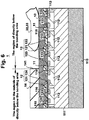
- the emitter electrode is formed on an interlayer insulation film between gate electrodes and the interlayer insulation film covers the gate electrode and has a stripe shaped aperture (contact hole) in a gate length direction on the region of the part of the emitter region and base region which is exposed. That is, in a cross section taken in a gate width direction, a plane shape of an interlayer insulation film of a projection which has a gap in adjacent interlayer insulation films by this aperture becomes a stripe shape the same as the plane shape of the gate electrode. Because it is possible to increase the contact area between the emitter electrode and the emitter region, base region and increase current capacitance in an IGBT which has this type of stripe structure, it is possible to reduce the occurrence of electrical filed concentration and realize a large current and high resistance.
- An emitter electrode of an IGBT is electrically connected to an emitter lead (external terminal) via bonding wire, and a gate electrode is similarly electrically connected to a gate lead via bonding wire.
- a collector electrode for example a collector electrode arranged on the other main surface of a substrate is electrically connected to a collector lead.
- a wire bonding device is generally used for the bonding wire and bonded by thermal compression combined with ultrasonic vibration.
- IGBT is sealed together with the inner parts of each lead and assembled as a semiconductor device.
- JP 2005-303218 A relates to a semiconductor device and its manufacturing method to provide a technology which can improve a manufacturing yield of a semiconductor device for example an insulated gate bipolar transistor.
- This document discloses buried control gates for an insulated gate bipolar transistor.
- the gate electrode planar area (gate width dimension) is reduced on the main surface of the substrate, and the planar area (from a contact hole in a gate width direction to an adjacent next step contact hole) of the interlayer insulation film above the gate electrode is also reduced. That is, because the adhesion area between the substrate main surface and the interlayer insulation film is further reduced, tears or breaks are produced in the interlayer insulation film and gate electrode. Furthermore, in the case where the diameter of the bonding wire is increased in order to manage a large current in a semiconductor device, because the energy of ultrasonic vibration which is required for bonding increases, tears and breaks occur more significantly in the interlayer insulation film and gate electrode.
- the present invention attempts to solve the above stated problems. Therefore, the present invention provides a semiconductor device which can prevent breaks in an interlayer insulation film and electrode that arise with bonding while maintaining bonding strength. Furthermore, the present invention provides a semiconductor device and manufacturing method of the semiconductor device which has semiconductor elements with good electrical characteristics. Furthermore, the present invention provides a semiconductor device which can reduce manufacturing costs.
- the present invention provides a semiconductor device which can prevent breaks in an interlayer insulation film and electrode that arise with bonding while maintaining bonding strength as well as maintain breakage tolerance.
- a first feature related to an embodiment of the present invention is a semiconductor device including a substrate having a first edge and a second edge opposing each other in a first direction and a third edge and a fourth edge opposing each other in a second direction which intersects the first direction, a plurality of first semiconductor regions arranged in the second direction on the substrate and exposing a first main surface and having a first conductivity, a plurality of second semiconductor regions arranged in the second direction within the first semiconductor region and exposing a second main surface on the first main surface of the first semiconductor region and having a second conductivity, a control electrode arranged between the second semiconductor region of the first semiconductor region and other second semiconductor regions of other first semiconductor regions which are adjacent in the second direction, an interlayer insulation film having an aperture part which exposes the first main surface of the first semiconductor region and the second main surface of the second semiconductor region, the aperture part having an aperture shape defined by a connection part
- Another feature related to an embodiment of the present invention is a semiconductor device including a hole which extends in the first direction and is arranged between the second semiconductor region of the first semiconductor region and other second semiconductor regions of other first semiconductor regions adjacent in the second direction and which penetrates the first semiconductor region on the substrate side from the first main surface of the first semiconductor region, and an insulation film arranged on a side surface of the hole and the bottom surface of the hole, wherein the control electrode is buried in the hole via the insulation film.
- Another feature related to an embodiment of the present invention is a semiconductor device including a third semiconductor region arranged between the second semiconductor region of the first semiconductor region and other second semiconductor regions of other first semiconductor regions adjacent in the second direction, and exposing a third main surface and having a second conductivity, and an insulation film arranged on the third main surface of the third semiconductor region, wherein the control electrode is arranged on the third main surface of the third semiconductor region via the insulation film.
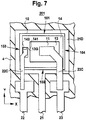
- Another feature related to an embodiment of the present invention is the semiconductor device according to the first feature wherein the interlayer insulation film is formed in a mesh shape by the extension part, the connection part and the aperture part.
- connection part of the interlayer insulation film is arranged in a region directly below a bonding area of the electrode.
- Another feature related to an embodiment of the present invention is the semiconductor device according to the first feature, wherein external wiring of a wire or a clip lead is electrically connected to the electrode.
- a second feature related to an embodiment of the present invention is a method of manufacturing a semiconductor device including forming a substrate having a first edge and a second edge opposing each other in a first direction and a third edge and a fourth edge opposing each other in a second direction which intersects the first direction, a plurality of first semiconductor regions arranged in the second direction on the substrate and exposing a first main surface and having a first conductivity, a plurality of second semiconductor regions arranged in the second direction within the first semiconductor region and exposing a second main surface on the first main surface of the first semiconductor region and having a second conductivity, a control electrode arranged between the second semiconductor region of the first semiconductor region and other second semiconductor regions of other first semiconductor regions which are adjacent in the second direction, forming an interlayer insulation film having an aperture part which exposes the first main surface of the first semiconductor region and the second main surface of the second semiconductor region, the aperture part having an aperture shape defined by a connection part which connects at fixed intervals in the first direction extension parts adjacent in the second direction, the extension part
- Another feature of an embodiment of the present invention related to the second feature is the method of manufacturing a semiconductor device, wherein forming an interlayer insulation film is forming the interlayer insulation film in which the connection part is arranged in a region directly below a bonding area, and forming the external wiring is forming the external wiring which is electrically connected to the electrode in the bonding area.
- a third feature related to an embodiment of the present invention is a semiconductor device including a semiconductor region having a first conductivity, a plurality of second semiconductor regions arranged in a second direction and exposing a first main surface and giving a second conductivity opposite to the first conductivity, a plurality of third semiconductor regions arranged in the second direction within the second semiconductor region, exposing a second surface within the second semiconductor region and having the first conductivity, a control electrode arranged between the third semiconductor region of the second semiconductor region and other third semiconductor regions of other second semiconductor regions which are adjacent in the second direction, an interlayer insulation film having an aperture part which exposes the first main surface of the first semiconductor region and the second main surface of the third semiconductor region, the aperture part having an aperture shape defined by a connection part which connects at fixed intervals in the first direction extension parts adjacent in the second direction, the extension part extending in the first direction which intersects the second direction and covering the top of the control electrode, and an electrode arranged on the interlayer insulation film and which electrically connects the first main surface of the second semiconductor region and the second
- Another feature related to the third feature of an embodiment of the present invention is the semiconductor device wherein the aperture part penetrates the third semiconductor region.
- Another feature related to the third feature of an embodiment of the present invention is the semiconductor device wherein the first width dimension and the second width dimension satisfies the following relationship formula; Second width dimension ⁇ 2.0 ⁇ first width dimension ⁇ 2.6 ⁇ first width dimension
- the semiconductor device further including a hole which extends in the first direction and is arranged between the third semiconductor region of the second semiconductor region and other third semiconductor regions of other second semiconductor regions adjacent in the second direction and which penetrates the second semiconductor region on the first semiconductor region side from the first main surface of the second semiconductor region, and an insulation film arranged on a side surface of the hole and the bottom surface of the hole, wherein the control electrode is buried in the hole via the insulation film.
- connection part of the interlayer insulation film is arranged in a region directly below a bonding area of the electrode.
- a fourth feature related to an embodiment of the present invention is a method of manufacturing a semiconductor device including forming a semiconductor region having a first conductivity, a plurality of second semiconductor regions arranged in a second direction and exposing a first main surface and giving a second conductivity opposite to the first conductivity, a plurality of third semiconductor regions arranged in the second direction within the second semiconductor region, exposing a second surface within the second semiconductor region and having the first conductivity, a control electrode arranged between the third semiconductor region of the second semiconductor region and other third semiconductor regions of other second semiconductor regions which are adjacent in the second direction, forming an interlayer insulation film having an aperture part which exposes the first main surface of the first semiconductor region and the second main surface of the third semiconductor region, the aperture part having an aperture shape defined by a connection part which connects at fixed intervals in the first direction extension parts adjacent in the second direction, the extension part extending in the first direction which intersects the second direction and covering the top of the control electrode, forming an electrode arranged on the interlayer insulation film and which electrically connects the first
- the present invention it is possible to provide a semiconductor device which can prevent breaks in an interlayer insulation film and electrode that arise with bonding while maintaining bonding strength. Furthermore, according to the present invention, it is possible to provide a semiconductor device which has semiconductor elements with good electrical characteristics. Furthermore, according to the present invention, it is possible to provide a semiconductor device which can reduce manufacturing costs.
- the first embodiment of the present invention explains an example which applies the present invention to a power semiconductor device and manufacturing method of the semiconductor device mounted with semiconductor elements comprised of an IGBT having a trench structure.
- a semiconductor element 1 mounted on a semiconductor device related to the first embodiment is arranged with a substrate 111 (specifically, refer to Fig. 1 and Fig. 4 ) having a first edge 101 and a second edge 102 which face each other in a first direction and a third edge 103 and a fourth edge 104 which face each other in a second direction which intersects the first direction, a plurality of first semiconductor regions 112 (specifically, refer to Fig. 1 and Fig.
- a gate electrode (control electrode) 116 arranged between the second semiconductor region 113 of the first semiconductor region 112 and other second semiconductor region 113 of other first semiconductor region 112 adjacent to the second direction, an interlayer insulation film 12 (specifically, refer to Fig. 1 and Fig.
- an aperture part 123 having an opening shape which is defined by an extension part 121 which covers the gate electrode 116 and extends in the first direction, a connection part 122, the extension part 121 and the connection part 122 which connects at fixed intervals in the first direction a pair of extension parts 121 which are adjacent to the second direction, and which exposes the first main surface of the first semiconductor region 112 and the second main surface of the second semiconductor region 113, and an electrode 13 arranged on the interlayer insulation film 12 and electrically connected to the first main surface of the first semiconductor region 112 and the second main surface of the second semiconductor surface 113.
- the semiconductor element 1 is an IGBT 11 and in the present embodiment this IGBT 11 is formed by an IGBT having a trench gate structure as shown in Fig. 1 and Fig. 2 . That is, the IGBT 11 is arranged with a p type semiconductor region 110 which is a contact region (or drain region (below called a contact region 110)), a substrate 111 (below called base region 111) which is an n type base region and an n type first semiconductor region, a type first semiconductor 112 which is a p type base region (below called base region 112), an n type second semiconductor region 113 which is an emitter region (below called emitter region 113), a hole (trench) 114, a gate insulation film 115, a gate electrode 116, a contact electrode (first electrode), and an emitter electrode (second electrode) 13.
- gate electrode means an electrode in which the flow of a main current can be controlled, and if the flow of a main current can be controlled then this includes a semiconductor region, a
- the base region (substrate) 111 is formed with a planar shape having a first edge 101 and a second edge 102 opposing each other in the first direction and a third edge 104 and a fourth edge 104 opposing each other in second direction.
- the base region 111 in the manufacturing process of the semiconductor element 1, is cut out from a silicon single crystal wafer by a dicing process after manufacturing the IGBT (cell) 11, and is a semiconductor chip.
- the planar shape of the base region 111 is not always limited to this planar shape.
- the base region 111 may be formed by a planar rectangle in which the first edge 101 and the second edge 102 are long edges and the third edge 103 and the fourth edge 104 are short edges.
- first direction is an up down direction in Fig. 2 , Fig. 3 and Fig. 4 , and is also a Y direction.
- second direction is a left to right direction in the same diagrams and is an X direction.
- an n type silicon single crystal substrate is used as the base region 111.
- a p type semiconductor region 110 is formed by diffusing p type impurities in the one main surface (bottom side surface) of this silicon single crystal substrate by epitaxial growth of a diffusion method. This p type semiconductor region 110 functions as a contact region of the IGBT 11.
- the p type base region 112 is formed by diffusing p type impurities in the main surface of the n type base region 111 by an impurity diffusion method.
- the emitter region (or source region) 113 is formed by diffusing n type impurities in a main surface part of the p type base region 112.
- the hole 114 penetrates the p type base region 112 heading in a depth direction (substrate side) from the main surface of the emitter region 113 and has a depth which reaches the n type base region 111 as is shown in Fig. 1 . Furthermore, as is shown in Fig. 2 , the length direction of the hole 114 extends heading in a first direction from the first edge 101 to the second edge 102, and a plurality of these holes 114 are arranged in rows at fixed intervals in the second direction heading from the third edge 103 to the fourth edge 104.
- the planar shape of the hole 114 has a stripe shape.
- the hole 114 for example, is formed using an isotropic etching such as reactive ion etching (RIE).
- the gate insulation film 115 is arranged along the inner wall and bottom surface of the hole 114.
- a silicon oxide film formed using a film formation method such as a thermal oxidation method or CVD method can be used as the gate insulation film 115.
- a compound film formed by combining a silicon nitride film, silicon oxide film and a silicon oxide film can also be used as the gate insulation film 115.
- the gate electrode 116 is buried within the hole 114 via the gate insulation film 115.
- the gate electrode 116 is formed using an etching method or a chemical mechanical polishing method (CMP).
- CMP chemical mechanical polishing method
- each of the emitter region 113 and the p type base region 112 which are between adjacent gate electrodes 116 in the second direction extend in the first direction the same as the extending direction of the gate electrode 116 other than the interior of a bonding area, and a plurality of the emitter regions 113 and the p type base regions 112 are arranged in rows in the second direction.
- the planar shape of the emitter region 113 and the p type base region 112 are formed in a stripe shape other than in the interior of a bonding area.
- the planar shape of he interlayer insulation film 12 related to the first embodiment is a mesh shape which has an extension part 121 is arranged at fixed intervals in the second direction within a bonding area of the second electrode 13 and is arranged between a second electrode 13 and gate electrode 116 extending in the first direction, a connecting part 122 which links with an adjacent extension part 121 and an aperture part 123.
- the planar shape of the interlayer insulation film 12 is a stripe shape in which only the extension part 121 is formed between the second electrode 13 and gate electrode 116 outside of the bonding area of the second electrode 13.
- the mesh shape of the interlayer insulation film 12 means arranged with the planar shape extension part 121 which has a stripe shape arranged on the gate electrode 116 (hole 114), extends in the same direction as the first direction in which the gate electrode 116 extends and is arranged in rows at fixed intervals in the second direction the same as the gate electrode 116, connecting part 122 formed as one part by linking with an adjacent extension part 121 in the second direction, and the aperture 123 formed in a region which is surrounded by two adjacent extension parts 121 in the second direction and two adjacent connecting parts 122 in the first direction.
- connection part 122 connects adjacent extension parts 121 in the second direction at fixed intervals in the first direction, it is possible to improve mechanical strength within the bonding area of the second electrode 13 in the interlayer insulation film 12 and the gate electrode 116 directly below. Specifically, it is possible to prevent cracks and tears in the extension part 121 and the gate electrode 116 directly below it with respect to stress which is generated when bonding (for example, ultrasound vibration energy).
- the connecting part 122 of the interlayer insulation film 12 is arranged between adjacent extension parts 121 in the second direction, however, the connecting part 122 is arranged within the bonding area, and because aperture 123 is arranged as much as possible in the mesh shape also within the bonding area, it is possible to reduce contact area and current capacitance between the emitter 131 and the second electrode 13 and also prevent electrical field concentration.
- the interlayer insulation film 12 it is possible to practically use a silicon oxide film, specifically, a phosphosilicate glass (PSG) film as the interlayer insulation film 12, and the thickness of this phosphosilicate glass film is set at 0.5 ⁇ m to 3.0 ⁇ m for example.
- PSG phosphosilicate glass
- the planar shape of the interlayer insulation film 12 which is set in the mesh shape is a region in which a bonding wire (32) which electrically connects the second electrode (emitter electrode) 13 with an emitter lead is bonded.
- a protection film 14 is arranged on the second electrode 13, an aperture 141 is arranged on the protection film and passed through the bonding wire (32), and the bonding area of the second electrode 13 is within the region of the aperture 141 which is arranged in the protective film 14.
- the planar shape of the interlayer insulation film 12 outside the bonding area of the second electrode 13 is a stripe shape as stated previously.
- the interlayer insulation film 12 is arranged with a plurality of planar shaped extension parts 121 which has a stripe shape arranged on the gate electrode 116 (hole 114), extends on the same direction as the first direction in which the gate electrode 116 extends, and is arranged at fixed intervals in the second direction the same as the arrangement intervals as the gate electrode 116, and a plurality of apertures 124 having a planar stripe shape formed within a region surrounded by adjacent extension parts 121 in the second direction and arranged at fixed intervals in the second direction.
- a connecting part 122 is not arranged between adjacent extension parts 121 in the second direction.
- the second electrode (emitter electrode) 13 is arranged on the interlayer insulation film 12 and also electrically connects the emitter region 113 of the IGBT 11 and the p type base region 112. Within the bonding area of the second electrode 13 the second electrode 13 is connected to the IGBT 11 via the aperture 123 of the interlayer insulation film 12 and outside the bonding area of the second electrode 13 is connected to the IGBT via the aperture 124 of the interlayer insulation layer 12.
- the second electrode 13 is used as an emitter electrode (or source electrode) and it is possible to use an aluminum alloy film for example as the second electrode 13.
- the aluminum alloy film is an aluminum which is added with additives such as Cu which prevents migration and Si which prevents alloy spikes.
- the protection film 14 is arranged on the second electrode 13 in the entire region on the main surface of the substrate 10.
- in aperture 141 is arranged in the bonding area on the second electrode 13 in the element region.
- a bonding electrode 13G for electrically connecting to the gate electrode 118 of the IGBT 11 is exposed by the aperture 142 of the protection film 14.
- the bonding electrode 13G of the gate electrode 116 is formed by the same conduction material in the same conduction layer as the second electrode 13.
- the aperture 141 of the protection film 14 is arranged at the center part of the base region (substrate) 111 as is shown in Fig. 4 , and the aperture 142 is arranged near in the third edge 103 of the base region 111.
- the planar area of the aperture 142 is small compared to the planar area of the aperture 141.
- a resin film or PSG film such as PIF (poly-imide film) for example can be used as the protection film 14.
- the semiconductor device 201 is arranged with a first lead (collector lead) 21 which extends in a first direction (Y direction) having a die bonding region 21D in which a semiconductor element 1 is mounted, a second lead (gate lead) 22 which extends in the first direction and is adjacent to left side of the first lead 21, a third lead (emitter lead) 23 which extends in the first direction and is adjacent to the right side of the first lead, a bonding wire 31 which electrically connects the second lead and the bonding electrode 13G of the semiconductor element 1, a bonding wire 32 which electrically connects the third lead and a bonding area of the second electrode 13 of the semiconductor element 1, and a sealing body 4.
- the resistance and inductance component of a metal plate or an alloy plate is small compared to a wire.
- stress generated in a bonding part of the metal plate, allot plate and a bonding area is large.
- the mechanical strength in the bonding area of the second electrode 13 is high. Therefore, in the semiconductor device 201, the resistance and inductance component is reduced, and it is possible to prevent tears in the interlayer insulation film 12 and tears in the gate electrode 116.
- the first electrode on the back surface of the semiconductor element 1 is electrically and mechanically connected to the bonding region 21D of the first lead 21 via a conduction adhesive.
- the bonding wire 31 penetrates the aperture 142 which is formed on the protection film 14 of the semiconductor element 1 and is electrically connected to the bonding electrode 13G.
- the bonding wire 32 penetrates the aperture 141 which is formed on the protection film 14 above the substrate 10 and is electrically connected to the electrode 13.
- a wire of Au, Lu, Al for example can be practically used as the bonding wire 31 and 32 and it is possible to bond the wires using thermal compression and ultrasound vibration using a bonding device.
- An epoxy resin for example can be used as the sealing body 4.
- This epoxy resin is formed for example by a molding method.
- the bonding wires 31 and 32 and an inner part (one part) of each of the semiconductor 1, the first lead 21, the second lead 22 and the third lead 23 are air tight sealed within the sealing body 4.
- An outer part (one part) of each of the first lead 21, the second lead 22 and the third lead 23 projects out from the exterior of the sealing body 4.
- the planar structure of the interlayer insulation film 12 within the bonding area is formed in a mesh shape, and because the mechanical strength increases by the connection part 122, the extension part 121 adjacent in a second direction of the interlayer insulation film 12, bonding strength of the interlayer insulation film 12 when bonding is secured, and tears which occur in the interlayer insulation film 12 with bonding and breaks in an electrode (for example, the gate electrode 116 and the second electrode 13) are prevented.
- connection part 122 of the interlayer insulation film 12 is arranged at fixed intervals in the second direction, it is possible to sufficiently secure the planar area of the aperture 123. Therefore, because it is possible to sufficiently secure the contact area which is the original characteristic of the IGBT 11, it is possible to reduce an electric filed concentration, secure sufficient resistance and provide a semiconductor device 201 with the semiconductor element 1 which has good electrical characteristics.
- the planar shape of the interlayer insulation film 12 outside the bonding area is formed in a stripe shape, it is possible to secure the electrical characteristics of the semiconductor element 1 as stated previously.
- the semiconductor device 1 related to the first embodiment because it is possible to change the planar shape of the interlayer insulation film 12 for demonstrating these operation effects simply by changing the pattern of a manufacturing mask, there is no particular need to increase the number of manufacturing processes, and it is possible to reduce manufacturing costs. Furthermore, because it is not necessary to increase the thickness of the second electrode 13 and bonding electrode 13G for bonding, it is also possible to reduce manufacturing costs in this way.
- the planar shape particularly within the bonding area of the interlayer insulation film 12 of the IGBT 11, as is shown in Fig. 5 is formed by a mesh shape formed as needed so that an aperture 123 arranged at fixed intervals in the first direction and an aperture 123 which is adjacent in the second direction are on the same straight line. That is, the connection part 122 is formed in one straight line when seen in the second direction, and when seen in the first direction is formed repeatedly at fixed intervals, and the planar shape of the interlayer insulation film 12 related to the transformation example un offset the arrangement pitch of the connection part 122 and aperture 123.
- the planar shape of the interlayer insulation film 12 only within a bonding area of the semiconductor element 1 is formed in a mesh shape.
- the present invention is not limited to the type of structure and the planar shape of the interlayer insulation film within and outside the bonding area can be a mesh shape.
- the second embodiment of the present invention explains an example in which the present invention is applied to a power semiconductor device and manufacturing method of the semiconductor device mounted with a semiconductor element comprised of an IGBT having a planar structure.
- the semiconductor element 1 mounted on the semiconductor device 201 related to the second embodiment, as shown in Fig. 6 is formed by an IGBT 11 having a planar structure. That is, the IGBT 11 is formed by arranging a collector region (p type second semiconductor region) 110, an n type base region (n type first semiconductor region or substrate) 111, a p type base region (p type first semiconductor region) 112, an emitter region (n type second semiconductor region) 113, a gate insulation film 115, a gate electrode 116, a collector electrode (first electrode) and an emitter electrode (second electrode) 13.
- a cross sectional structure of a basic semiconductor element 1 is the same as the cross sectional structure of the semiconductor element 1 of the semiconductor device 201 related to the first embodiment stated previously.
- the hole 114 shown in Fig. 1 is not arranged. That is, the semiconductor element 1, the gate electrode 116 is arranged with a planar structure via the gate insulation film 114 on the main surface of the base region 111, and a base region 112 and emitter region 113 are arranged by a double diffusion structure with the gate electrode 116 as a mask.
- the interlayer insulation film 12 is formed similar to the semiconductor device 201 related to the first embodiment shown in Fig. 1 to Fig. 4 stated previously, by a planar shaped extension part 121 having a stripe shape extending in the same direction as a first direction in which the gate electrode 118 extends, and arranged on the gate electrode at fixed intervals in a second direction the same as the arrangement intervals of the gate electrode 116, a planar shaped connection part 121 having a stripe shape, a connection part 122 which is connected with the extension part 121 adjacent in the second direction and formed as one unit, and an aperture 123 formed within a region surrounded by two extension parts 121 adjacent in the second direction and two connection parts 122 adjacent in the first direction. That is, the planar shape of the interlayer insulation 12 is formed in a mesh shape within at least the bonding area of the second electrode 13.
- the planar structure of the interlayer insulation film 12 within the bonding area of the second electrode 13 is formed in a mesh shape, and because the extension part 121 adjacent in the second direction of the interlayer insulation film 12 is connected with the connection part 122 and mechanical strength increases, the bonding strength of the interlayer insulation film 12 is secured when bonding and it is possible to prevent breaks in the interlayer insulation film 12 and breaks in an electrode (for example, gate electrode 116 or second electrode 13) that comes with bonding.
- an electrode for example, gate electrode 116 or second electrode 13
- connection part 122 of the interlayer insulation film 12 is arranged at fixed intervals in the second direction, it is possible to sufficiently secure the planar area (contact area) of the aperture 123. Therefore, because it is possible to sufficiently secure the contact area and current capacitance which is the original characteristic of the semiconductor element 1 having a stripe structure, it is possible to reduce an electric filed concentration, secure sufficient resistance and provide a semiconductor device 201 with the semiconductor element 1 which has good electrical characteristics.
- the semiconductor device 201 related to the second embodiment by forming the planar shape of the interlayer insulation film 12 outside the bonding area of the second electrode 13 in a stripe shape shown in Fig. 3 , it is possible to secure the electrical characteristics of the semiconductor element 1.
- the semiconductor device 201 related to the second embodiment because it is possible to change the planar shape of the interlayer insulation film 12 for demonstrating these operation effects simply by changing the pattern of a manufacturing mask, there is no particular need to increase the number of manufacturing processes, and it is possible to reduce manufacturing costs.
- the third embodiment of the present invention explains an example in which the connection method between the semiconductor element 1 with the second lead 22 and the third lead 23 is replaced in the semiconductor device 201 related to the first embodiment and the second embodiment stated previously.
- soldering paste 35 is used in each of the connections between the clip lead 22C and the bonding electrode 13G and the second clip lead 22, and each are electrically and mechanically connected.
- soldering paste 36 is used in each of the connections between the clip lead 23C and the second electrode 13 and the third clip lead 23, and each are electrically and mechanically connected.
- an alloy plate such as a Cu plate or an alloy plate such as a Fe ⁇ Ni plate for example for the clip lead 22C and the clip lead 23C.
- Pb ⁇ Sn solder or Pb free solder such as Sn- 3 wt % Ag ⁇ 0.5 wt % Cu for the soldering paste 35 and 36. Similar to the bonding of the bonding wire 31, a bonding method where thermal compression is combined with ultrasound vibrations is used in the connection of the clip lead 22 to the bonding electrode 13G via the soldering paste 35, and the connection of the clip lead 22C to the second lead 22 via the soldering paste 35.
- a bonding method which combines thermal compression with ultrasound vibrations similar to a heating method using a heater or bonding of the bonding wire 32, is used in the connection of the clip lead 23C to the second electrode 13 via the soldering paste 36, and the connection of the clip lead 23C to the third lead 23 via the soldering paste 36.
- a wetability improvement film can be formed on the surface of each of the bonding electrode 13G and the second electrode 13. It is possible to practically use a compound layer stacked with an Ni layer on a Ti layer for example as the wettability improvement film.
- the resistance and inductance component of a metal plate or alloy plate of the clip lead 22C and 23C is small compared to a wire. Reversely, stress generated at the bonding part between a metal plate or alloy plate and a bonding area is large.
- a connection part 122 is arranged on the interlayer insulation layer 12 in the bonding area of the second electrode 13 in the third embodiment, it is possible to increase mechanical strength in the bonding area of the second electrode 13. Therefore, in the semiconductor device 201 the resistance and inductance component can be reduced and it is possible to prevent tears in the interlayer insulation film and tears in the gate electrode 116.
- the fourth embodiment of the present invention explains an example in which the present invention is applied to a power semiconductor device and manufacturing method of the semiconductor device mounted with a semiconductor element comprised of an IGBT having a trench structure.
- the semiconductor element 1 (semiconductor chip) mounted in the semiconductor device related to the fourth embodiment includes a first edge 101 and a second edge 102 which face each other and extend in a second direction (X direction) and a third edge 103 and a fourth edge 104 which face each other and extend in a first direction (Y direction) which intersects the second direction, a first semiconductor region (substrate) 111 (specifically, refer to Fig. 11 and Fig.
- the aperture part 123 continues in order to pass through the third semiconductor region 113 with the interlayer insulation film 12 as a mask.
- a first width dimension 121W below the extension part 121 or in a second direction of the third semiconductor region 113 which contacts with the extension part 121 compared with a second width dimension 122W of the first direction of the third semiconductor region 113 which contacts with a connection part 122 below the connection part 122 is set large.
- Fig. 9 and Fig. 10 a first width dimension 121W below the extension part 121 or in a second direction of the third semiconductor region 113 which contacts with the extension part 121 compared with a second width dimension 122W of the first direction of the third semiconductor region 113 which contacts with a connection part 122 below the connection part 122 is set large.
- the first width dimension 121W of the third semiconductor region 113 is dimension from the end of the aperture part 123 side of the extension part 121 on the interlayer insulation film 12 to the gate electrode film 115.
- the second width dimension 122W of the third semiconductor region 113 is equivalent to the width dimension of the main surface side which contact with the third semiconductor region 113 of the connection part 112.
- the semiconductor element 1 is an IGBT 11 and this IGBT 11 is formed from an IGBT having a trench gate structure in the fourth embodiment as is shown in Fig. 11 and Fig. 2 . That is, the IGBT 11 is arranged with a p type fourth semiconductor region 110 which is a collector region (or drain region) (below called a collector region 110), a first semiconductor region 111 (below called base region 111) which is an n type base region and an n type first semiconductor region, a p type second semiconductor 112 which is a p type base region (called base region 112 below), an n type third semiconductor region 113 which is an emitter region (below called emitter region 113), a hole (trench) 114, a gate insulation film 115, a gate electrode 116, a collector electrode (first electrode) which is arranged on the entire bottom surface of the collector region 110, and an emitter electrode (second electrode) 13.
- gate electrode is used with the same meaning as the gate electrode explained in the first embodiment.
- the base region (substrate) 111 is formed with a planar shape having a first edge 101 and a second edge 102 opposing each other in the first direction and a third edge 104 and a fourth edge 104 opposing each other in second direction.
- the base region 111 in the manufacturing process of the semiconductor element 1, is cut out from a silicon single crystal wafer by a dicing process after manufacturing the IGBT (cell) 11, and is a semiconductor chip.
- the planar shape of the base region 111 is not always limited to this planar shape.
- the base region 111 may be formed by a planar rectangle in which the first edge 101 and the second edge 102 are long edges and the third edge 103 and the fourth edge 104 are short edges.
- first direction and second direction are used with the same meaning as the first direction and second direction explained in the first embodiment.
- the planar shape of the interlayer insulation layer 12 related to the fourth embodiment is a mesh shape which, within the bonding area of the first electrode 13, includes a plurality of extension parts 121 arranged at fixed intervals in the second direction and arranged between the second electrode 12 and gate electrode 116 which extend in the first direction, a connection part 122 which connects an adjacent connection part 121, and an aperture 123.
- the planar shape of the interlayer insulation film 12 outside of the bonding area of the first electrode 13 only the extension part 121 which is formed between the second electrode 13 and the gate electrode 116 has a stripe shape.
- the mesh shape of the interlayer insulation film 12 means a planar shaped extension part 121 having a stripe shape and arranged on the gate electrode 116 (hole 114), extending in the same direction as the first direction in which the gate electrode 116 extends and arranged at fixed intervals in the second direction the same as the gate electrode 116, a connecting part 122 formed as one part by linking with an adjacent extension part 121 in the second direction, and the aperture 123 formed in a region which is surrounded by two adjacent extension parts 121 in the second direction and two adjacent connecting parts 122 in the first direction.
- connection part 122 is connects adjacent extension parts 121 in the second direction at fixed intervals in the first direction, it is possible to improve the mechanical strength of the extension part 121 of the interlayer insulation film 12 and the gate electrode 116 directly below it within the bonding area of the second electrode 13. In particular, it is possible to prevent cracks and tears in the extension part 121 and the gate electrode 116 directly below it with respect to stress which is generated when bonding (for example, ultrasound vibration energy).
- the connecting part 122 of the interlayer insulation film 12 is arranged between adjacent extension parts 121 in the second direction, however, the connecting part 122 is arranged within the bonding area, and because aperture 123 is arranged as much as possible in a mesh shape also within the bonding area, it is possible to reduce contact area and current capacitance between the emitter 131 and the second electrode 13 and also prevent electrical field concentration.
- the manufacturing becomes easier and manufacturing costs do not increase.
- the fourth embodiment it is possible to practically use a silicon oxide film, specifically, a phosphosilicate glass (PSG) film as the interlayer insulation film 12, and the thickness of this phosphosilicate glass film is set at 0.5 ⁇ m to 3.0 ⁇ m for example.
- PSG phosphosilicate glass
- Fig. 12 the causal relationship between the aperture ratio and the defect ratio of the aperture 123 of the interlayer insulation film 12 is shown in Fig. 12 .
- the horizontal axis shows the aperture ratio of the aperture 123 of the interlayer insulation film 12
- the left vertical axis shows the defect ratio (%) due to avalanche damage
- the right vertical axis shows the defect ratio (%) due to wire bonding damage.
- the aperture ratio of the aperture 123 of the interlayer insulation film 12 increases, that is, when the second width dimension 122W of the connection part 122 increases with respect to the first width dimension 121W of the extension part 121, it is possible to reduce the defect ratio caused by wire bonding damage.
- the defect ratio effectively becomes 0 (zero) when the aperture ratio is 2.2 in the curve A and the aperture ratio in the curve B is 2.0 shown in Fig. 12 . That is, it is possible to prevent cracks and tears in the extension part 121 of the interlayer insulation film 12 and the gate electrode 116 directly below it.
- the wire bonding conditions of curve A are the bonding load is 1200 g/cm 2 , ultrasound vibration energy (ultrasound power) is 145 Hz at a first side, and 190 Hz at a second side, and the ultrasound vibration time is 120 msec at the first side and 170 msec at the second side.
- the wire bonding conditions of curve B are the bonding load is 1200 glcm 2 , ultrasound vibration energy (ultrasound power) is 145 Hz at a first side, and 180 Hz at a second side, and the ultrasound vibration time is 120 msec at the first side and 170 msec at the second side.
- the aperture ratio of the aperture 123 of the interlayer insulation film 122 increases, that is when the second width dimension 122W of the connection part 122 increases with respect to the first width dimension 121W of the extension part 121 increases, the defect ratio caused by avalanche damage increases when the aperture ratio is 2.6 as a border as is shown in the curve C.
- a current path is shortest from a bonding wire on the region in which the third semiconductor region 113 is exposed.
- the current path becomes longer from the center (for example, shown by K in Fig. 10 ) of the connection part 122 to the third semiconductor 113 and the dynamic time lag of a current becomes larger.
- the amount of avalanche tolerance it is important that the energy which is applied is diffused over a larger area, the current concentration is relaxed and a parasitic transistor is not switched ON. Within this, lowering the resistance of the second semiconductor region 112 directly below the third semiconductor region 113 is effective. Because etching is performed until one part of the third semiconductor region 113 is passed through with the interlayer insulation film as a mask, the aperture 123 and the resistance of the second semiconductor region 112 directly below the third semiconductor region 113 has a close relationship. That is, based on the causal relationship shown in Fig.
- the planar shape of the interlayer insulation film 12 is adopted so that a mesh shape in which the aperture 123 arranged at fixed intervals in the first direction and an aperture 123 adjacent in a second direction are offset.
- the amount of offset is half an arrangement pitch for example.
- bonding area of the second electrode 12 in which the planar shape of the interlayer insulation film is set in a mesh shape means a region in which a bonding wire (32) which electrically connects the second electrode (emitter electrode) 13 and an emitter lead (external terminal) is bonded.
- a protection film 14 is arranged on the second electrode 13, an aperture 141 for electrically connecting the bonding wire (32) with the second electrode 13 is arranged on the protection film 14 as is shown in Fig. 11 , and the bonding area of the second electrode 13 is within a region of the aperture 141 set in the protection film 14.
- the planar shape of the interlayer insulation film 12 outside the bonding area of the second electrode 13 is a stripe shape.
- the interlayer insulation film 12 is arranged with a plurality of planar shaped extension part 121 having a stripe shape arranged above gate electrode 116 (or hole 114) extending in the same direction as the first direction in which the gate electrode 115 extends and arranged at fixed intervals in a second direction the same as the arrangement direction of the gate electrode 116, and a plurality of aperture parts 124 having a planar shape sandwiched between adjacent extension parts 121 in the second direction and arranged at firs intervals in the second direction.
- connection part 122 between adjacent extension parts 121 in the second direction.
- connection part 122 because it is possible to increase the aperture area of the aperture part 124, it is possible to secure contact area and current capacitance between the emitter region 113 and the second electrode 13 and prevent electric field concentration.
- the second electrode (emitter electrode) 13 is arranged on the interlayer insulation film 12 and within the bonding area of the second electrode 13, the second electrode 13 is connected to the IGBT 11 via the aperture 123 of the interlayer insulation film 12, Outside the bonding area of the second electrode 13, the second electrode is connected to the IGBT 11 via the aperture 124 of the interlayer insulation film 12.
- the second electrode 13 is used as an emitter electrode (or source electrode) and a aluminum alloy film for example can be used as the second electrode 13.
- the aluminum alloy film is an aluminum added with additives such as Si for preventing alloy spike, or Cu for preventing migration.
- the protection film 14 is arranged on the second electrode 13 in the entire region above the main surface of the substrate 10. In an element region, the aperture 141 is arranged in a bonding area of the second electrode 13. In addition, as is shown in Fig. 4 , in the protection film 14, in an element region, the bonding electrode 13G for connecting to the gate electrode 116 of the IGBT 11 is exposed by the aperture 142 of the protection film 14. The bonding electrode 13G of the gate electrode 116 is formed by the same conduction material in the same conduction layer as the second electrode 13. The aperture 141 of the protection film 14 is arranged at the center part of the base region (substrate) 111 as is shown in Fig.
- the aperture 142 is arranged near the third edge 103 of the base region 111.
- the planar area of the aperture 142 is small compared to the planar area of the aperture 141. It is possible to practically use a resin film such as PIF (polyimide ⁇ film) or PSG film for example as the protection film 14.
- the semiconductor device 201 related to the fourth embodiment is arranged with a semiconductor element 1, a first lead (collector external terminal) 21 which extends in a first direction (X direction) having a die bonding region 21D in which a semiconductor element 1 is mounted, a second lead (gate external terminal) 22 which extends in the first direction and is arranged to left side of the first lead 21, a third lead (emitter external terminal) 23 which extends in the first direction and is arranged to the right side of the first lead, a bonding wire 31 which electrically connects the second lead and the bonding electrode 13G of the semiconductor element 1, a bonding wire 32 which electrically connects the third lead and a bonding area of the second electrode 13 of the semiconductor element 1, and a sealing body 4.
- Ni plating may also be used on the surface of the Cu plate.
- the first electrode of the back surface of the semiconductor element 1 is electrically and mechanically connected to the die bonding region 21D of the first lead 21 via a conduction adhesive.
- the bonding wire 31 is electrically connected to the bonding region 13G via the aperture 142 which is formed on the protection film 14 of the semiconductor element 1.
- the bonding wire 32 is electrically connected to the electrode 13 via the aperture 141 which is formed on the protection film above the substrate 10.
- a wire of Au, Lu, Al can be practically used as the bonding wire 31, 32 and this wire is bonded by combining thermal compression with ultrasound vibrations used a bonding device.
- An epoxy resin for example can be used as the sealing body 4.
- This epoxy resin is formed for example by a molding method.
- An inner part (one part) of each of the semiconductor 1m the first lead 21, the second lead 22 and the third lead 23 and the bonding wires 31, 32 are air tight sealed within the sealing body 4.
- An outer part (one part) of each of the first lead 21, the second lead 22 and the third lead 23 projects out from the exterior of the sealing body 4.
- the assembly sequence of the semiconductor device 201 is as follows. First, the semiconductor element 1 is manufactured formed with the IGBT 11, interlayer insulation film 12, second electrode 13 and protection film 14 in this order. Next, the semiconductor element 1 is installed on the die bonding region 21D of the first lead 21. Next, the bonding wires 31 and 32 are bonded. Then, the semiconductor device 201 related to the fourth embodiment is completed by molding the semiconductor element 1 by the sealing body 4.
- the planar structure of the interlayer insulation film 12 within the bonding area is formed in a mesh shape, and because the mechanical strength increases by the connection part 122, the extension part 121 adjacent in a second direction of the interlayer insulation film 12, bonding strength of the interlayer insulation film 12 when bonding is secured, and tears which occur in the interlayer insulation film 12 with bonding and breaks in an electrode (for example, the gate electrode 116 and the second electrode 13) are prevented.
- connection part 122 of the interlayer insulation film 12 is arranged at fixed intervals in the second direction, it is possible to sufficiently secure the planar area of the aperture 123. Therefore, because it is possible to sufficiently secure the contact area which is the original characteristic of the IGBT 11, it is possible to reduce an electric filed concentration, secure sufficient resistance and provide a semiconductor device 201 with the semiconductor element 1 which has good electrical characteristics.
- the ratio between the first width dimension 121W below the extension part 121 (or the extension part 121) of the third semiconductor region 113, and the second width dimension 122W below the connection part (or the connection part 122) of the third semiconductor region 113 is set within an appropriate range, it is possible to secure the bonding strength of the interlayer insulation film 12 when bonding and secure sufficient resistance.
- the planar shape of the interlayer insulation film 12 outside the bonding area is formed in a stripe shape, it is possible to secure the electrical characteristics of the semiconductor element 1 as stated previously.
- the semiconductor device 1 related to the fourth embodiment because it is possible to change the planar shape of the interlayer insulation film 12 for demonstrating these operation effects simply by changing the pattern of a manufacturing mask, there is no particular need to increase the number of manufacturing processes, and it is possible to reduce manufacturing costs. Furthermore, because it is not necessary to increase the thickness of the second electrode 13 and bonding electrode 13G for bonding, it is also possible to reduce manufacturing costs in this way.
- the planar shape particularly within the bonding area of the interlayer insulation film 12 of the IGBT 11, similar to the semiconductor device 201 related to the first embodiment shown in Fig. 8 , is formed as needed by a mesh shape so that an aperture 123 arranged at fixed intervals in the first direction and an aperture 123 which is adjacent in the second direction are on the same straight line. That is, the connection part 122 is formed in one straight line when seen in the second direction, and when seen in the first direction is formed repeatedly at fixed intervals, and the planar shape of the interlayer insulation film 12 related to the transformation example un-offset the arrangement pitch of the connection part 122 and aperture 123.
- the planar shape of the interlayer insulation film 12 only within a bonding area of the semiconductor element 1 is formed in a mesh shape.
- the present invention is not limited to the type of structure and the planar shape of the interlayer insulation film within and outside the bonding area can be a mesh shape.
- the fifth embodiment of the present invention is a transformation example of a power semiconductor device and manufacturing method of the semiconductor device related to the fourth embodiment and explains an example in which the present invention is applied to a power semiconductor device and manufacturing method of the semiconductor device mounted with a semiconductor element comprised of an IGBT having a planar structure.
- the semiconductor element 1 mounted on the semiconductor device 201 related to the fifth embodiment, as shown in Fig. 13 is formed by an IGBT 11 having a planar structure. That is, the IGBT 11 is formed by arranging a collector region (p type fourth semiconductor region) 110, an n type base region (n type second semiconductor region or substrate) 111, a p type base region (p type second semiconductor region) 112, an emitter region (n type third semiconductor region) 113, a gate insulation film 115, a gate electrode 116, a collector electrode (first electrode) and an emitter electrode (second electrode) 13.
- a cross sectional structure of a basic semiconductor element 1 is the same as the cross sectional structure of the semiconductor element 1 of the semiconductor device 201 related to the fourth embodiment stated previously.
- the hole 114 shown in Fig. 9 and Fig. 10 is not arranged. That is, in the semiconductor element 1, the gate electrode 116 is arranged with a planar structure via the gate insulation film 114 on the main surface of the base region 111, and a base region 112 and emitter region 113 are arranged by a double diffusion structure with the gate electrode 116 as a mask.
- the sixth embodiment of the present invention explains an example in which the connection method between the semiconductor element 1 with the second lead 22 and the third lead 23 is replaced in the semiconductor device 201 related to the fourth embodiment and the fifth embodiment stated previously.
- soldering paste 35 is used in each of the connections between the clip lead 22C and the bonding electrode 13G and the second clip lead 22, and each are electrically and mechanically connected.
- soldering paste 35 is used in each of the connections between the clip lead 23C and the second electrode 13 and the third clip lead 23, and each are electrically and mechanically connected.
- an alloy plate such as a Cu plate or an alloy plate such as a Fe-Ni plate for example for the clip lead 22C and the clip lead 23C.
- Pb ⁇ Sn solder or Pb free solder such as Sn ⁇ 3 wt % Ag ⁇ 0.5 wt % Cu for the soldering paste 35 and 36. Similar to the bonding of the bonding wire 31, a bonding method where thermal compression is combined with ultrasound vibrations is used in the connection of the clip lead 22 to the bonding electrode 13G via the soldering paste 35, and the connection of the clip lead 22C to the second lead 22 via the soldering paste 35.
- a bonding method which combines thermal compression with ultrasound vibrations similar to a heating method using a heater or bonding of the bonding wire 32, is used in the connection of the clip lead 23C to the second electrode 13 via the soldering paste 36, and the connection of the clip lead 23C to the third lead 23 via the soldering paste 36.
- a wetability improvement film can be formed on the surface of each of the bonding electrode 13G and the second electrode 13. It is possible to practically use a compound layer stacked with an Ni layer on a Ti layer for example as the wettability improvement film.
- the resistance and inductance component of a metal plate or alloy plate of the clip lead 22C and 23C is small compared to a wire. Reversely, stress generated at the bonding part between a metal plate or alloy plate and a bonding area is large.
- a connection part 122 is arranged on the interlayer insulation layer 12 in the bonding area of the second electrode 13 in the sixth embodiment, it is possible to increase mechanical strength in the bonding area of the second electrode 13. Therefore, in the semiconductor device 201 the resistance and inductance component can be reduced and it is possible to prevent tears in the interlayer insulation film and tears in the gate electrode 116.
- the present invention can be applied to various alternative forms, embodiments and technologies.
- an example of the semiconductor device 201 mounted with the semiconductor element 1 comprised of the IGBT 11 the present invention is not limited to the IGBT 11.
- the present invention can also be applied to a semiconductor element comprised of a power transistor having not only a trench structure but also a planar structure and a semiconductor device mounted with this semiconductor element.
- the corner part of the aperture 123 of the interlayer insulation film 123 may be round.
- the present invention can be widely used in a semiconductor device and manufacturing method of the semiconductor device in which it is necessary to prevent damage of interlayer insulation film and damage of an electrode which is generated with bonding while securing bonding strength.
- the present invention can be widely used in a semiconductor device and manufacturing method of the semiconductor device in which it is necessary to prevent damage of interlayer insulation film and damage of an electrode which is generated with bonding while comparatively securing damage tolerance and bonding strength.
- the present invention can be widely used in a semiconductor device and manufacturing method of the semiconductor device in which it is necessary to improve the electrical characteristics of a semiconductor element.
- the present invention can be widely used in a semiconductor device and manufacturing method of the semiconductor device in which it is necessary to reduce manufacturing costs.
Description
- The present invention is related to a semiconductor device. In particular, the present invention is related to a semiconductor device in which external wiring is connected to an electrode of semiconductor elements.
- Semiconductor elements such as an IGBT (insulated gate bipolar transistor) and a power MOSFET (metal oxide semiconductor field effect transistor) are incorporated into a semiconductor device. This type of semiconductor element is a switching device which can control a large current at high speeds.
- A semiconductor element, for example, an IGBT, is arranged with a collector region, a base region, an emitter region, a gate insulation film and a gate electrode. The collector region is formed by epitaxial growth on one main surface of a substrate or by diffusion in one main surface part of the substrate. The base region is formed in the other main part of the substrate. The emitter region is formed on the surface part of the base region. The gate insulation film is formed on at least the surface of the base region and the gate electrode is formed on the gate insulation film.
- By forming the gate electrode in the shape of a stripe, an IGBT with a stripe structure having a high resistance and small gate capacitance is adopted as a semiconductor element. In the IGBT which adopts this structure, the gate electrode extends on the substrate main surface in a gate length direction, a plurality of the gate electrodes is arranged in series at fixed intervals in the gate width direction, and seen from above, one part of the surface of the emitter region and base region is exposed in a stripe shape in a gate length direction in between the gate electrodes in the gate width direction. An emitter electrode (emitter wiring) is electrically connected to the emitter region and base region in which the surface is exposed. The emitter electrode is formed on an interlayer insulation film between gate electrodes and the interlayer insulation film covers the gate electrode and has a stripe shaped aperture (contact hole) in a gate length direction on the region of the part of the emitter region and base region which is exposed. That is, in a cross section taken in a gate width direction, a plane shape of an interlayer insulation film of a projection which has a gap in adjacent interlayer insulation films by this aperture becomes a stripe shape the same as the plane shape of the gate electrode. Because it is possible to increase the contact area between the emitter electrode and the emitter region, base region and increase current capacitance in an IGBT which has this type of stripe structure, it is possible to reduce the occurrence of electrical filed concentration and realize a large current and high resistance.
- An emitter electrode of an IGBT is electrically connected to an emitter lead (external terminal) via bonding wire, and a gate electrode is similarly electrically connected to a gate lead via bonding wire. A collector electrode, for example a collector electrode arranged on the other main surface of a substrate is electrically connected to a collector lead. A wire bonding device is generally used for the bonding wire and bonded by thermal compression combined with ultrasonic vibration. In addition, IGBT is sealed together with the inner parts of each lead and assembled as a semiconductor device.
- Furthermore, this type of semiconductor device is described in, for example, patent document 1 (
JP 10 022322 A JP 2002 222826A JP 2005-303218 A - However, in the semiconductor stated above, the following points were not considered. When bonding wire which is directly connected to an emitter electrode directly above the IGBT which has a stripe structure is bonded by ultrasonic vibration, tears or breaks occur in an interlayer insulation film or a gate electrode below of the IGBT (cell) below the interlayer insulation film. Specifically, in the IGBT, because a planar shape of the gate electrode and interlayer insulation film has a long thin stripe shape in the gate length direction, the mechanical strength of the gate electrode and the interlayer insulation film is weak and the adhesion area with the ground is small. Moreover, because it has a shape which projects out from the substrate main surface, when the bonding wire is bonded, tears and breaks are produced in the interlayer insulation film and gate electrode. Particularly, when the above stated problem easily occurs when stress is produced in the interlayer insulation film in the gate width direction.
- In addition, with the miniaturization of the IGBT, when a trench structure is adopted, the gate electrode planar area (gate width dimension) is reduced on the main surface of the substrate, and the planar area (from a contact hole in a gate width direction to an adjacent next step contact hole) of the interlayer insulation film above the gate electrode is also reduced. That is, because the adhesion area between the substrate main surface and the interlayer insulation film is further reduced, tears or breaks are produced in the interlayer insulation film and gate electrode. Furthermore, in the case where the diameter of the bonding wire is increased in order to manage a large current in a semiconductor device, because the energy of ultrasonic vibration which is required for bonding increases, tears and breaks occur more significantly in the interlayer insulation film and gate electrode.
- When such tears and breaks are produced in the interlayer insulation film and gate electrode, insulation defects occur between the emitter electrode (emitter region) and gate electrode. In extreme cases, a short circuit occurs between the emitter electrode and gate electrode.
- In order to reduce tears and breaks in the interlayer insulation film and gate electrode, there is a method for weakening the ultrasonic power of the bonding device (during the bonding process) and there is a method for reducing pressure load. However, in the case of adopting this type of method, a sufficient bonding strength (mechanical bonding strength) cannot be obtained between the emitter electrode and the bonding wire. In the case where the binding strength is insufficient, tears occur in the bonding wire from the emitter electrode when resin sealing in the manufacture of the semiconductor device or during operation of the semiconductor device.
- In addition, in order to reduce tears and breaks in the interlayer insulation film and gate electrode in the semiconductor element side, there is a method of not arranging an IGBT (cell) in a region in which bonding wire is bonded, and a method for forming an emitter electrode with a thin aluminum film. However, in the former method, because a cell does not exist in a region in a part of the substrate, either an ON voltage which has important electrical characteristics of the IGBT is significantly increased, or the size of the semiconductor elements increases. In addition, in the later method, it is possible to absorb the effects when bonding the bonding wire by the emitter electrode or prevent the effects from propagating under the emitter electrode. However, in the semiconductor manufacturing process, manufacturing costs increase together with an increase in material costs and increase in electrode film formation time. Furthermore, an increase in film thickness of the emitter electrode is linked to an increase in film stress due to the operations of the semiconductor elements and a change in the electrical characteristics of the IGBT is produced because unnecessary stress is added to the IGBT.
- The present invention attempts to solve the above stated problems. Therefore, the present invention provides a semiconductor device which can prevent breaks in an interlayer insulation film and electrode that arise with bonding while maintaining bonding strength. Furthermore, the present invention provides a semiconductor device and manufacturing method of the semiconductor device which has semiconductor elements with good electrical characteristics. Furthermore, the present invention provides a semiconductor device which can reduce manufacturing costs.
- In addition, the present invention provides a semiconductor device which can prevent breaks in an interlayer insulation film and electrode that arise with bonding while maintaining bonding strength as well as maintain breakage tolerance.
- In order to solve the above stated problems, the present invention provides a semiconductor device as claimed in
claim 1. Preferred embodiments are defined in the dependent claims.
A first feature related to an embodiment of the present invention is a semiconductor device including a substrate having a first edge and a second edge opposing each other in a first direction and a third edge and a fourth edge opposing each other in a second direction which intersects the first direction, a plurality of first semiconductor regions arranged in the second direction on the substrate and exposing a first main surface and having a first conductivity, a plurality of second semiconductor regions arranged in the second direction within the first semiconductor region and exposing a second main surface on the first main surface of the first semiconductor region and having a second conductivity, a control electrode arranged between the second semiconductor region of the first semiconductor region and other second semiconductor regions of other first semiconductor regions which are adjacent in the second direction, an interlayer insulation film having an aperture part which exposes the first main surface of the first semiconductor region and the second main surface of the second semiconductor region, the aperture part having an aperture shape defined by a connection part which connects at fixed intervals in the first direction extension parts adjacent in the second direction, the extension part extending in the first direction and covering the top of the control electrode, and an electrode arranged on the interlayer insulation film and which electrically connects the first main surface of the first semiconductor region and the second main surface of the second semiconductor region via the aperture part of the interlayer insulation film. - Another feature related to an embodiment of the present invention is a semiconductor device including a hole which extends in the first direction and is arranged between the second semiconductor region of the first semiconductor region and other second semiconductor regions of other first semiconductor regions adjacent in the second direction and which penetrates the first semiconductor region on the substrate side from the first main surface of the first semiconductor region, and an insulation film arranged on a side surface of the hole and the bottom surface of the hole, wherein the control electrode is buried in the hole via the insulation film.
- Another feature related to an embodiment of the present invention is a semiconductor device including a third semiconductor region arranged between the second semiconductor region of the first semiconductor region and other second semiconductor regions of other first semiconductor regions adjacent in the second direction, and exposing a third main surface and having a second conductivity, and an insulation film arranged on the third main surface of the third semiconductor region, wherein the control electrode is arranged on the third main surface of the third semiconductor region via the insulation film.
- Another feature related to an embodiment of the present invention is the semiconductor device according to the first feature wherein the interlayer insulation film is formed in a mesh shape by the extension part, the connection part and the aperture part.
- Another feature related to an embodiment of the present invention is the semiconductor device according to the first feature, wherein the connection part of the interlayer insulation film is arranged in a region directly below a bonding area of the electrode.
- Another feature related to an embodiment of the present invention is the semiconductor device according to the first feature, wherein external wiring of a wire or a clip lead is electrically connected to the electrode.
- A second feature related to an embodiment of the present invention is a method of manufacturing a semiconductor device including forming a substrate having a first edge and a second edge opposing each other in a first direction and a third edge and a fourth edge opposing each other in a second direction which intersects the first direction, a plurality of first semiconductor regions arranged in the second direction on the substrate and exposing a first main surface and having a first conductivity, a plurality of second semiconductor regions arranged in the second direction within the first semiconductor region and exposing a second main surface on the first main surface of the first semiconductor region and having a second conductivity, a control electrode arranged between the second semiconductor region of the first semiconductor region and other second semiconductor regions of other first semiconductor regions which are adjacent in the second direction, forming an interlayer insulation film having an aperture part which exposes the first main surface of the first semiconductor region and the second main surface of the second semiconductor region, the aperture part having an aperture shape defined by a connection part which connects at fixed intervals in the first direction extension parts adjacent in the second direction, the extension part extending in the first direction and covering the top of the control electrode, forming an electrode arranged on the interlayer insulation film and which electrically connects the first main surface of the first semiconductor region and the second main surface of the second semiconductor region via the aperture of the interlayer insulation film, and forming external wiring which is electrically connected to the electrode on the electrode.
- Another feature of an embodiment of the present invention related to the second feature is the method of manufacturing a semiconductor device, wherein forming an interlayer insulation film is forming the interlayer insulation film in which the connection part is arranged in a region directly below a bonding area, and forming the external wiring is forming the external wiring which is electrically connected to the electrode in the bonding area.
- A third feature related to an embodiment of the present invention is a semiconductor device including a semiconductor region having a first conductivity, a plurality of second semiconductor regions arranged in a second direction and exposing a first main surface and giving a second conductivity opposite to the first conductivity, a plurality of third semiconductor regions arranged in the second direction within the second semiconductor region, exposing a second surface within the second semiconductor region and having the first conductivity, a control electrode arranged between the third semiconductor region of the second semiconductor region and other third semiconductor regions of other second semiconductor regions which are adjacent in the second direction, an interlayer insulation film having an aperture part which exposes the first main surface of the first semiconductor region and the second main surface of the third semiconductor region, the aperture part having an aperture shape defined by a connection part which connects at fixed intervals in the first direction extension parts adjacent in the second direction, the extension part extending in the first direction which intersects the second direction and covering the top of the control electrode, and an electrode arranged on the interlayer insulation film and which electrically connects the first main surface of the second semiconductor region and the second main surface of the third semiconductor region via the aperture part of the interlayer insulation film, wherein a second width dimension in the first direction of the third semiconductor region below the connection part is larger than a first width dimension in the second direction of the third semiconductor region below the extension part.
- Another feature related to the third feature of an embodiment of the present invention is the semiconductor device wherein the aperture part penetrates the third semiconductor region.
- Another feature related to the third feature of an embodiment of the present invention is the semiconductor device wherein the first width dimension and the second width dimension satisfies the following relationship formula;

- Another feature related to the third feature of an embodiment of the present invention is the semiconductor device, further including a hole which extends in the first direction and is arranged between the third semiconductor region of the second semiconductor region and other third semiconductor regions of other second semiconductor regions adjacent in the second direction and which penetrates the second semiconductor region on the first semiconductor region side from the first main surface of the second semiconductor region, and an insulation film arranged on a side surface of the hole and the bottom surface of the hole, wherein the control electrode is buried in the hole via the insulation film.
- Another feature related to the third feature of an embodiment of the present invention is the semiconductor device, wherein the connection part of the interlayer insulation film is arranged in a region directly below a bonding area of the electrode.
- A fourth feature related to an embodiment of the present invention is a method of manufacturing a semiconductor device including forming a semiconductor region having a first conductivity, a plurality of second semiconductor regions arranged in a second direction and exposing a first main surface and giving a second conductivity opposite to the first conductivity, a plurality of third semiconductor regions arranged in the second direction within the second semiconductor region, exposing a second surface within the second semiconductor region and having the first conductivity, a control electrode arranged between the third semiconductor region of the second semiconductor region and other third semiconductor regions of other second semiconductor regions which are adjacent in the second direction, forming an interlayer insulation film having an aperture part which exposes the first main surface of the first semiconductor region and the second main surface of the third semiconductor region, the aperture part having an aperture shape defined by a connection part which connects at fixed intervals in the first direction extension parts adjacent in the second direction, the extension part extending in the first direction which intersects the second direction and covering the top of the control electrode, forming an electrode arranged on the interlayer insulation film and which electrically connects the first main surface of the second semiconductor region and the second main surface of the third semiconductor region via the aperture part of the interlayer insulation film, and forming external wiring which electrically connects the electrode on the electrode in the bonding area.
- According to the present invention, it is possible to provide a semiconductor device which can prevent breaks in an interlayer insulation film and electrode that arise with bonding while maintaining bonding strength. Furthermore, according to the present invention, it is possible to provide a semiconductor device which has semiconductor elements with good electrical characteristics. Furthermore, according to the present invention, it is possible to provide a semiconductor device which can reduce manufacturing costs.
- In addition, according to the present invention, it is possible to provide a semiconductor device which can prevent breaks in an interlayer insulation film and electrode that arise with bonding while maintaining bonding strength as well as maintain breakage tolerance.
-
-
Fig. 1 is an expanded cross sectional diagram of important parts when arranging a bonding wire on semiconductor elements mounted on a semiconductor device related to a first embodiment of the present invention. -
Fig. 2 is an expanded planar diagram of the important parts (one part of the IGBT except a protection film, bonding wire, second electrode and interlayer insulation film) of the semiconductor elements inFig. 1 . -
Fig. 3 is an expanded planar diagram of the important parts of the interlayer insulation film in the semiconductor elements shown inFig. 1 . -
Fig. 4 is a planar diagram which shows the internal structure of the semiconductor device related to the first embodiment. -
Fig. 5 is an expanded planar diagram of the important parts of the interlayer insulation film in the semiconductor elements related to a transformation example of the first embodiment. -
Fig. 6 is an expanded cross sectional diagram of the important when arranging a bonding wire on semiconductor elements mounted on a semiconductor device related to a second embodiment of the present invention. -
Fig. 7 is a planar diagram which shows the internal structure of a semiconductor device related to a third embodiment of the present invention. -
Fig. 8 is an expanded cross sectional diagram of the important parts when arranging a clip lead on semiconductor elements of the semiconductor device shown inFig. 7 . -
Fig. 9 is an expanded oblique view diagram of the important parts of the semiconductor elements mounted on a semiconductor device related to a fourth embodiment of the present invention. -
Fig. 10 is an expanded planar diagram of the important parts of the semiconductor elements -
Fig. 11 is an expanded cross sectional diagram of the important parts when arranging a bonding wire on the semiconductor elements shown inFig. 9 . -
Fig. 12 is a diagram which shows the relationship between the aperture ratio and imperfection ratio of the interlayer insulation layer related to the fourth embodiment. -
Fig. 13 is an expanded cross sectional diagram of important parts when arranging bonding on semiconductor elements mounted on a semiconductor device related to a fifth embodiment of the present invention. -
Fig. 14 is an expanded cross sectional diagram of important parts when arranging a clip lead on semiconductor elements mounted on a semiconductor device related to a sixth embodiment of the present invention. - Next, the embodiments of the present invention will be explained while referring to the diagrams. The invention will be described with reference to the attached drawings. Like or corresponding parts are denoted by like or corresponding reference numerals. The drawings are schematic, and may sometimes differ from actual components. In addition, dimensions and ratios of components may be different between drawings.
- In addition, while the invention herein is disclosed by means of specific embodiments and applications thereof, numerous modifications and variations could be made thereto without departing from the scope of the invention set forth in the claims.
- The first embodiment of the present invention explains an example which applies the present invention to a power semiconductor device and manufacturing method of the semiconductor device mounted with semiconductor elements comprised of an IGBT having a trench structure.
- As is shown in
Fig. 1 andFig. 4 , a semiconductor element 1 mounted on a semiconductor device related to the first embodiment is arranged with a substrate 111 (specifically, refer toFig. 1 andFig. 4 ) having a first edge 101 and a second edge 102 which face each other in a first direction and a third edge 103 and a fourth edge 104 which face each other in a second direction which intersects the first direction, a plurality of first semiconductor regions 112 (specifically, refer toFig. 1 andFig. 4 ) arranged in the second direction on the substrate 111 and exposing a first main surface and having a first conductivity, a plurality of second semiconductor regions 113 arranged in the second direction within the first semiconductor region 112 and exposing a second main surface on the first main surface of the first semiconductor region 112 and having a second conductivity opposite to the first conductivity, a gate electrode (control electrode) 116 arranged between the second semiconductor region 113 of the first semiconductor region 112 and other second semiconductor region 113 of other first semiconductor region 112 adjacent to the second direction, an interlayer insulation film 12 (specifically, refer toFig. 1 andFig. 3 ) which has an aperture part 123 having an opening shape which is defined by an extension part 121 which covers the gate electrode 116 and extends in the first direction, a connection part 122, the extension part 121 and the connection part 122 which connects at fixed intervals in the first direction a pair of extension parts 121 which are adjacent to the second direction, and which exposes the first main surface of the first semiconductor region 112 and the second main surface of the second semiconductor region 113, and an electrode 13 arranged on the interlayer insulation film 12 and electrically connected to the first main surface of the first semiconductor region 112 and the second main surface of the second semiconductor surface 113. - The
semiconductor element 1 is anIGBT 11 and in the present embodiment thisIGBT 11 is formed by an IGBT having a trench gate structure as shown inFig. 1 andFig. 2 . That is, theIGBT 11 is arranged with a ptype semiconductor region 110 which is a contact region (or drain region (below called a contact region 110)), a substrate 111 (below called base region 111) which is an n type base region and an n type first semiconductor region, a typefirst semiconductor 112 which is a p type base region (below called base region 112), an n typesecond semiconductor region 113 which is an emitter region (below called emitter region 113), a hole (trench) 114, agate insulation film 115, agate electrode 116, a contact electrode (first electrode), and an emitter electrode (second electrode) 13. Here, gate electrode means an electrode in which the flow of a main current can be controlled, and if the flow of a main current can be controlled then this includes a semiconductor region, a diffusion region and an electrode. - The base region (substrate) 111, as is shown in
Fig. 4 , is formed with a planar shape having afirst edge 101 and asecond edge 102 opposing each other in the first direction and athird edge 104 and afourth edge 104 opposing each other in second direction. Thebase region 111, in the manufacturing process of thesemiconductor element 1, is cut out from a silicon single crystal wafer by a dicing process after manufacturing the IGBT (cell) 11, and is a semiconductor chip. The planar shape of thebase region 111 is not always limited to this planar shape. For example, thebase region 111 may be formed by a planar rectangle in which thefirst edge 101 and thesecond edge 102 are long edges and thethird edge 103 and thefourth edge 104 are short edges. - Here, in the first embodiment, first direction is an up down direction in
Fig. 2 ,Fig. 3 andFig. 4 , and is also a Y direction. In addition, second direction is a left to right direction in the same diagrams and is an X direction. - As is shown in
Fig. 1 , in the present embodiment an n type silicon single crystal substrate is used as thebase region 111. A ptype semiconductor region 110 is formed by diffusing p type impurities in the one main surface (bottom side surface) of this silicon single crystal substrate by epitaxial growth of a diffusion method. This ptype semiconductor region 110 functions as a contact region of theIGBT 11. - The p
type base region 112 is formed by diffusing p type impurities in the main surface of the ntype base region 111 by an impurity diffusion method. The emitter region (or source region) 113 is formed by diffusing n type impurities in a main surface part of the ptype base region 112. - The
hole 114 penetrates the ptype base region 112 heading in a depth direction (substrate side) from the main surface of theemitter region 113 and has a depth which reaches the ntype base region 111 as is shown inFig. 1 . Furthermore, as is shown inFig. 2 , the length direction of thehole 114 extends heading in a first direction from thefirst edge 101 to thesecond edge 102, and a plurality of theseholes 114 are arranged in rows at fixed intervals in the second direction heading from thethird edge 103 to thefourth edge 104. The planar shape of thehole 114 has a stripe shape. Thehole 114, for example, is formed using an isotropic etching such as reactive ion etching (RIE). - The
gate insulation film 115 is arranged along the inner wall and bottom surface of thehole 114. A silicon oxide film formed using a film formation method such as a thermal oxidation method or CVD method can be used as thegate insulation film 115. In addition, a compound film formed by combining a silicon nitride film, silicon oxide film and a silicon oxide film can also be used as thegate insulation film 115. - The
gate electrode 116 is buried within thehole 114 via thegate insulation film 115. In the first embodiment, for example, it is possible to practically use a silicon polycrystalline film in which n type impurities are introduced for securing conductivity as thegate electrode 116. After burying within thehole 114, thegate electrode 116 is formed using an etching method or a chemical mechanical polishing method (CMP). As is shown inFig. 2 , because the planar shape of thehole 114 is formed in a long thin stripe shape in the first direction, the planar shape of the gate electrode 16 is formed in a long thin stripe shape in a first direction according to the planar shape of thehole 114. - As is shown in
Fig. 2 , the surface region in which a connectingpart 112 of theinterlayer insulation film 121 is not formed is exposed on the surface of theemitter region 113 which is formed so as to sandwich thegate electrode 116. Similarly, the surface region in which the interlayer insulation film 121 (a connecting part 112) is not formed is exposed on the surface of the ptype base region 112. Therefore, each of theemitter region 113 and the ptype base region 112 which are betweenadjacent gate electrodes 116 in the second direction extend in the first direction the same as the extending direction of thegate electrode 116 other than the interior of a bonding area, and a plurality of theemitter regions 113 and the ptype base regions 112 are arranged in rows in the second direction. The planar shape of theemitter region 113 and the ptype base region 112 are formed in a stripe shape other than in the interior of a bonding area. - As is shown in
Fig. 1 to Fig. 4 , the planar shape of he interlayerinsulation film 12 related to the first embodiment, is a mesh shape which has anextension part 121 is arranged at fixed intervals in the second direction within a bonding area of thesecond electrode 13 and is arranged between asecond electrode 13 andgate electrode 116 extending in the first direction, a connectingpart 122 which links with anadjacent extension part 121 and anaperture part 123. In addition, the planar shape of theinterlayer insulation film 12 is a stripe shape in which only theextension part 121 is formed between thesecond electrode 13 andgate electrode 116 outside of the bonding area of thesecond electrode 13. - The mesh shape of the
interlayer insulation film 12 means arranged with the planarshape extension part 121 which has a stripe shape arranged on the gate electrode 116 (hole 114), extends in the same direction as the first direction in which thegate electrode 116 extends and is arranged in rows at fixed intervals in the second direction the same as thegate electrode 116, connectingpart 122 formed as one part by linking with anadjacent extension part 121 in the second direction, and theaperture 123 formed in a region which is surrounded by twoadjacent extension parts 121 in the second direction and two adjacent connectingparts 122 in the first direction. Because theconnection part 122 connectsadjacent extension parts 121 in the second direction at fixed intervals in the first direction, it is possible to improve mechanical strength within the bonding area of thesecond electrode 13 in theinterlayer insulation film 12 and thegate electrode 116 directly below. Specifically, it is possible to prevent cracks and tears in theextension part 121 and thegate electrode 116 directly below it with respect to stress which is generated when bonding (for example, ultrasound vibration energy). On the other hand, the connectingpart 122 of theinterlayer insulation film 12 is arranged betweenadjacent extension parts 121 in the second direction, however, the connectingpart 122 is arranged within the bonding area, and becauseaperture 123 is arranged as much as possible in the mesh shape also within the bonding area, it is possible to reduce contact area and current capacitance between the emitter 131 and thesecond electrode 13 and also prevent electrical field concentration. In addition, because it is possible to achieve these effects simply by changing the aperture pattern of theinterlayer insulation film 12, because a new process is not added to the manufacturing process, manufacturing becomes easier and manufacturing costs do not increase. In the first embodiment, it is possible to practically use a silicon oxide film, specifically, a phosphosilicate glass (PSG) film as theinterlayer insulation film 12, and the thickness of this phosphosilicate glass film is set at 0.5 µm to 3.0 µm for example. - An example of the sizes of each part related to the
interlayer insulation film 12 and the structure of theinterlayer insulation film 12 is as follows. -
- 1. hole width of the hole 114: 0.5 µm to 3.0 µm
- 2. arrangement pitch of the hole 114: 2.0 µm to 20.0 µm
- 3. width of the
extension part 121 of the interlayer insulation 12: 1.0 µm to 4.0 µm - 4. width of the connecting
part 122 of the interlayer insulation 12: 1.0 µm to 19.0 µm - 5. arrangement pitch of the connecting
part 122 in the first direction: 2.0 µm to 20.0 µm - 6.
aperture size 123 of the interlayer insulation film 12: 1.0 µm x 1.0 µm to 19.0 µm x 1.0 µm - 7. bonding area size: 50 µm x 50 µm to 2mm x 2mm
- Here, the planar shape of the
interlayer insulation film 12 which is set in the mesh shape (bonding area of the second electrode 13) is a region in which a bonding wire (32) which electrically connects the second electrode (emitter electrode) 13 with an emitter lead is bonded. Aprotection film 14 is arranged on thesecond electrode 13, anaperture 141 is arranged on the protection film and passed through the bonding wire (32), and the bonding area of thesecond electrode 13 is within the region of theaperture 141 which is arranged in theprotective film 14. - The planar shape of the
interlayer insulation film 12 outside the bonding area of thesecond electrode 13 is a stripe shape as stated previously. Specifically, theinterlayer insulation film 12 is arranged with a plurality of planar shapedextension parts 121 which has a stripe shape arranged on the gate electrode 116 (hole 114), extends on the same direction as the first direction in which thegate electrode 116 extends, and is arranged at fixed intervals in the second direction the same as the arrangement intervals as thegate electrode 116, and a plurality ofapertures 124 having a planar stripe shape formed within a region surrounded byadjacent extension parts 121 in the second direction and arranged at fixed intervals in the second direction. Because it is not necessary to increase mechanical strength against stress which is produced when bonding outside of the bonding area of thesecond electrode 13, a connectingpart 122 is not arranged betweenadjacent extension parts 121 in the second direction. As a result of not arranging the connectingpart 122, it is possible to increase the area of theaperture 124 and therefore it is possible to secure contact area and current capacitance between theemitter region 113 and thesecond electrode 13 and prevent an electrical field concentration. In addition, it is possible to achieve these effects simply by changing the aperture pattern of theinterlayer insulation film 12 and because a process is not added to the manufacturing process, manufacturing becomes easier and manufacturing costs do not increase. - The second electrode (emitter electrode) 13, is arranged on the
interlayer insulation film 12 and also electrically connects theemitter region 113 of theIGBT 11 and the ptype base region 112. Within the bonding area of thesecond electrode 13 thesecond electrode 13 is connected to theIGBT 11 via theaperture 123 of theinterlayer insulation film 12 and outside the bonding area of thesecond electrode 13 is connected to the IGBT via theaperture 124 of theinterlayer insulation layer 12. Thesecond electrode 13 is used as an emitter electrode (or source electrode) and it is possible to use an aluminum alloy film for example as thesecond electrode 13. The aluminum alloy film is an aluminum which is added with additives such as Cu which prevents migration and Si which prevents alloy spikes. - As is shown in
Fig. 1 , theprotection film 14 is arranged on thesecond electrode 13 in the entire region on the main surface of thesubstrate 10. As is shown inFig. 1 to Fig. 4 , in theprotection film 14, inaperture 141 is arranged in the bonding area on thesecond electrode 13 in the element region. In addition, in theprotection film 14 as is shown inFig. 4 , in the element region, abonding electrode 13G for electrically connecting to the gate electrode 118 of theIGBT 11 is exposed by theaperture 142 of theprotection film 14. Thebonding electrode 13G of thegate electrode 116 is formed by the same conduction material in the same conduction layer as thesecond electrode 13. Theaperture 141 of theprotection film 14 is arranged at the center part of the base region (substrate) 111 as is shown inFig. 4 , and theaperture 142 is arranged near in thethird edge 103 of thebase region 111. The planar area of theaperture 142 is small compared to the planar area of theaperture 141. A resin film or PSG film such as PIF (poly-imide film) for example can be used as theprotection film 14. - As is shown in
Fig. 4 , thesemiconductor device 201 is arranged with a first lead (collector lead) 21 which extends in a first direction (Y direction) having a diebonding region 21D in which asemiconductor element 1 is mounted, a second lead (gate lead) 22 which extends in the first direction and is adjacent to left side of thefirst lead 21, a third lead (emitter lead) 23 which extends in the first direction and is adjacent to the right side of the first lead, abonding wire 31 which electrically connects the second lead and thebonding electrode 13G of thesemiconductor element 1, abonding wire 32 which electrically connects the third lead and a bonding area of thesecond electrode 13 of thesemiconductor element 1, and a sealingbody 4. - It is possible to use a Cu plate or a Fe-Ni alloy plate as the
first lead 21,second lead 22 andthird lead 23. Here, the resistance and inductance component of a metal plate or an alloy plate is small compared to a wire. However, stress generated in a bonding part of the metal plate, allot plate and a bonding area is large. However, in the first embodiment, because aconnection part 122 is arranged on theinterlayer insulation film 12 in the bonding area of thesecond electrode 13, the mechanical strength in the bonding area of thesecond electrode 13 is high. Therefore, in thesemiconductor device 201, the resistance and inductance component is reduced, and it is possible to prevent tears in theinterlayer insulation film 12 and tears in thegate electrode 116. - Although not shown in detail in
Fig. 1 to Fig. 4 , the first electrode on the back surface of thesemiconductor element 1 is electrically and mechanically connected to thebonding region 21D of thefirst lead 21 via a conduction adhesive. - The
bonding wire 31 penetrates theaperture 142 which is formed on theprotection film 14 of thesemiconductor element 1 and is electrically connected to thebonding electrode 13G. Similarly, thebonding wire 32 penetrates theaperture 141 which is formed on theprotection film 14 above thesubstrate 10 and is electrically connected to theelectrode 13. A wire of Au, Lu, Al for example can be practically used as thebonding wire - An epoxy resin for example can be used as the sealing
body 4. This epoxy resin is formed for example by a molding method. Thebonding wires semiconductor 1, thefirst lead 21, thesecond lead 22 and thethird lead 23 are air tight sealed within the sealingbody 4. An outer part (one part) of each of thefirst lead 21, thesecond lead 22 and thethird lead 23 projects out from the exterior of the sealingbody 4. - As is shown in
Fig. 1 to Fig. 4 , in thesemiconductor device 201 related to the first embodiment, the planar structure of theinterlayer insulation film 12 within the bonding area is formed in a mesh shape, and because the mechanical strength increases by theconnection part 122, theextension part 121 adjacent in a second direction of theinterlayer insulation film 12, bonding strength of theinterlayer insulation film 12 when bonding is secured, and tears which occur in theinterlayer insulation film 12 with bonding and breaks in an electrode (for example, thegate electrode 116 and the second electrode 13) are prevented. - Furthermore, in the
semiconductor device 201 related to the first embodiment, because theconnection part 122 of theinterlayer insulation film 12 is arranged at fixed intervals in the second direction, it is possible to sufficiently secure the planar area of theaperture 123. Therefore, because it is possible to sufficiently secure the contact area which is the original characteristic of theIGBT 11, it is possible to reduce an electric filed concentration, secure sufficient resistance and provide asemiconductor device 201 with thesemiconductor element 1 which has good electrical characteristics. - In addition, in the
semiconductor device 201 related to the first embodiment, because the planar shape of theinterlayer insulation film 12 outside the bonding area is formed in a stripe shape, it is possible to secure the electrical characteristics of thesemiconductor element 1 as stated previously. - In addition, in the
semiconductor device 1 related to the first embodiment, because it is possible to change the planar shape of theinterlayer insulation film 12 for demonstrating these operation effects simply by changing the pattern of a manufacturing mask, there is no particular need to increase the number of manufacturing processes, and it is possible to reduce manufacturing costs. Furthermore, because it is not necessary to increase the thickness of thesecond electrode 13 andbonding electrode 13G for bonding, it is also possible to reduce manufacturing costs in this way. - In the
semiconductor device 1 related to a transformation example of the first embodiment, the planar shape particularly within the bonding area of theinterlayer insulation film 12 of theIGBT 11, as is shown inFig. 5 , is formed by a mesh shape formed as needed so that anaperture 123 arranged at fixed intervals in the first direction and anaperture 123 which is adjacent in the second direction are on the same straight line. That is, theconnection part 122 is formed in one straight line when seen in the second direction, and when seen in the first direction is formed repeatedly at fixed intervals, and the planar shape of theinterlayer insulation film 12 related to the transformation example un offset the arrangement pitch of theconnection part 122 andaperture 123. - In the
semiconductor device 201 related to the transformation example formed in this way, the same effects can be demonstrated as the effects obtained by thesemiconductor device 201 related to the first embodiment stated previously. - Furthermore, in the
semiconductor device 201 related to the first embodiment, the planar shape of theinterlayer insulation film 12 only within a bonding area of thesemiconductor element 1 is formed in a mesh shape. However, the present invention is not limited to the type of structure and the planar shape of the interlayer insulation film within and outside the bonding area can be a mesh shape. - The second embodiment of the present invention, explains an example in which the present invention is applied to a power semiconductor device and manufacturing method of the semiconductor device mounted with a semiconductor element comprised of an IGBT having a planar structure.
- The
semiconductor element 1 mounted on thesemiconductor device 201 related to the second embodiment, as shown inFig. 6 , is formed by anIGBT 11 having a planar structure. That is, theIGBT 11 is formed by arranging a collector region (p type second semiconductor region) 110, an n type base region (n type first semiconductor region or substrate) 111, a p type base region (p type first semiconductor region) 112, an emitter region (n type second semiconductor region) 113, agate insulation film 115, agate electrode 116, a collector electrode (first electrode) and an emitter electrode (second electrode) 13. A cross sectional structure of abasic semiconductor element 1 is the same as the cross sectional structure of thesemiconductor element 1 of thesemiconductor device 201 related to the first embodiment stated previously. However, thehole 114 shown inFig. 1 is not arranged. That is, thesemiconductor element 1, thegate electrode 116 is arranged with a planar structure via thegate insulation film 114 on the main surface of thebase region 111, and abase region 112 andemitter region 113 are arranged by a double diffusion structure with thegate electrode 116 as a mask. - The
interlayer insulation film 12 is formed similar to thesemiconductor device 201 related to the first embodiment shown inFig. 1 to Fig. 4 stated previously, by a planar shapedextension part 121 having a stripe shape extending in the same direction as a first direction in which the gate electrode 118 extends, and arranged on the gate electrode at fixed intervals in a second direction the same as the arrangement intervals of thegate electrode 116, a planar shapedconnection part 121 having a stripe shape, aconnection part 122 which is connected with theextension part 121 adjacent in the second direction and formed as one unit, and anaperture 123 formed within a region surrounded by twoextension parts 121 adjacent in the second direction and twoconnection parts 122 adjacent in the first direction. That is, the planar shape of theinterlayer insulation 12 is formed in a mesh shape within at least the bonding area of thesecond electrode 13. - As is shown in the
Fig. 6 , in thesemiconductor device 201 related to the second embodiment, the same as thesemiconductor device 201 related to the first embodiment stated above, the planar structure of theinterlayer insulation film 12 within the bonding area of thesecond electrode 13 is formed in a mesh shape, and because theextension part 121 adjacent in the second direction of theinterlayer insulation film 12 is connected with theconnection part 122 and mechanical strength increases, the bonding strength of theinterlayer insulation film 12 is secured when bonding and it is possible to prevent breaks in theinterlayer insulation film 12 and breaks in an electrode (for example,gate electrode 116 or second electrode 13) that comes with bonding. - Furthermore, in the
semiconductor device 201 related to the second embodiment, because theconnection part 122 of theinterlayer insulation film 12 is arranged at fixed intervals in the second direction, it is possible to sufficiently secure the planar area (contact area) of theaperture 123. Therefore, because it is possible to sufficiently secure the contact area and current capacitance which is the original characteristic of thesemiconductor element 1 having a stripe structure, it is possible to reduce an electric filed concentration, secure sufficient resistance and provide asemiconductor device 201 with thesemiconductor element 1 which has good electrical characteristics. - In addition, in the
semiconductor device 201 related to the second embodiment, by forming the planar shape of theinterlayer insulation film 12 outside the bonding area of thesecond electrode 13 in a stripe shape shown inFig. 3 , it is possible to secure the electrical characteristics of thesemiconductor element 1. - In addition, in the
semiconductor device 201 related to the second embodiment, because it is possible to change the planar shape of theinterlayer insulation film 12 for demonstrating these operation effects simply by changing the pattern of a manufacturing mask, there is no particular need to increase the number of manufacturing processes, and it is possible to reduce manufacturing costs. - The third embodiment of the present invention explains an example in which the connection method between the
semiconductor element 1 with thesecond lead 22 and thethird lead 23 is replaced in thesemiconductor device 201 related to the first embodiment and the second embodiment stated previously. - In the
semiconductor device 201 related to the third embodiment, as is shown inFig. 7 andFig. 8 , thebonding electrode 13G and thesecond lead 22 of thesemiconductor element 1 are electrically connected by aclip lead 22C and thesecond electrode 13 and thethird lead 23 are electrically connected by aclip lead 23C. Solderingpaste 35 is used in each of the connections between theclip lead 22C and thebonding electrode 13G and thesecond clip lead 22, and each are electrically and mechanically connected. Similarly, solderingpaste 36 is used in each of the connections between theclip lead 23C and thesecond electrode 13 and thethird clip lead 23, and each are electrically and mechanically connected. - It is possible to use an alloy plate such as a Cu plate or an alloy plate such as a Fe·Ni plate for example for the
clip lead 22C and theclip lead 23C. It is possible to use Pb·Sn solder or Pb free solder such as Sn- 3 wt % Ag·0.5 wt % Cu for thesoldering paste bonding wire 31, a bonding method where thermal compression is combined with ultrasound vibrations is used in the connection of theclip lead 22 to thebonding electrode 13G via thesoldering paste 35, and the connection of theclip lead 22C to thesecond lead 22 via thesoldering paste 35. Similarly a bonding method which combines thermal compression with ultrasound vibrations similar to a heating method using a heater or bonding of thebonding wire 32, is used in the connection of theclip lead 23C to thesecond electrode 13 via thesoldering paste 36, and the connection of theclip lead 23C to thethird lead 23 via thesoldering paste 36. - In addition, in order to improve bondability of the
bonding electrode 13G and thesoldering paste 35, and in order to improve the bondability of thesecond electrode 13 and thesoldering paste 36, a wetability improvement film can be formed on the surface of each of thebonding electrode 13G and thesecond electrode 13. It is possible to practically use a compound layer stacked with an Ni layer on a Ti layer for example as the wettability improvement film. - In the
semiconductor device 201 related to third embodiment formed in this way, the same effects can be demonstrated as the effects obtained by thesemiconductor 201 related to the first and second embodiments stated previously. - Furthermore, the resistance and inductance component of a metal plate or alloy plate of the
clip lead connection part 122 is arranged on theinterlayer insulation layer 12 in the bonding area of thesecond electrode 13 in the third embodiment, it is possible to increase mechanical strength in the bonding area of thesecond electrode 13. Therefore, in thesemiconductor device 201 the resistance and inductance component can be reduced and it is possible to prevent tears in the interlayer insulation film and tears in thegate electrode 116. - The fourth embodiment of the present invention explains an example in which the present invention is applied to a power semiconductor device and manufacturing method of the semiconductor device mounted with a semiconductor element comprised of an IGBT having a trench structure.
- As is shown in
Fig. 9 to Fig. 11 andFig. 2 to Fig. 4 of the first embodiment, the semiconductor element 1 (semiconductor chip) mounted in the semiconductor device related to the fourth embodiment includes a first edge 101 and a second edge 102 which face each other and extend in a second direction (X direction) and a third edge 103 and a fourth edge 104 which face each other and extend in a first direction (Y direction) which intersects the second direction, a first semiconductor region (substrate) 111 (specifically, refer toFig. 11 andFig. 4 ) exposing a first main surface and having a first conductivity, a plurality of second semiconductor regions 112 arranged in the second direction on the first semiconductor region 111 and exposing a second main surface and having a second conductivity opposite to the first conductivity, a plurality of third semiconductor regions 113 (emitter region) arranged in the second direction within the second semiconductor region 112 and exposing a third main surface side of the second semiconductor region 112 and having a first conductivity, a gate electrode (control electrode) 116 arranged between the third semiconductor region 113 within the second semiconductor region 112 and another third semiconductor region 113 within another second semiconductor region 112 adjacent to the second direction, an interlayer insulation film 12 which has an aperture part 123 having an opening shape which is defined by an extension part 121 which covers the gate electrode 116 and extends in the first direction, a connection part 122, the extension part 121 and the connection part 122 which connects at fixed intervals in the first direction a pair of extension parts 121 which are adjacent to the second direction, and which exposes the first main surface of the second semiconductor region 112 and the second main surface of the third semiconductor region 113, and an electrode 13 (emitter electrode) arranged on the interlayer insulation film 12 and electrically connected to the first main surface of the second semiconductor region 112 and the second main surface of the third semiconductor surface 113. - Also, the
aperture part 123 continues in order to pass through thethird semiconductor region 113 with theinterlayer insulation film 12 as a mask. As is shown inFig. 9 andFig. 10 , afirst width dimension 121W below theextension part 121 or in a second direction of thethird semiconductor region 113 which contacts with theextension part 121 compared with asecond width dimension 122W of the first direction of thethird semiconductor region 113 which contacts with aconnection part 122 below theconnection part 122 is set large. As is shown inFig. 9 , because etching is performed until thethird semiconductor region 113 is passed through, thefirst width dimension 121W of thethird semiconductor region 113 is dimension from the end of theaperture part 123 side of theextension part 121 on theinterlayer insulation film 12 to thegate electrode film 115. In addition, thesecond width dimension 122W of thethird semiconductor region 113 is equivalent to the width dimension of the main surface side which contact with thethird semiconductor region 113 of theconnection part 112. - The
semiconductor element 1 is anIGBT 11 and thisIGBT 11 is formed from an IGBT having a trench gate structure in the fourth embodiment as is shown inFig. 11 andFig. 2 . That is, theIGBT 11 is arranged with a p typefourth semiconductor region 110 which is a collector region (or drain region) (below called a collector region 110), a first semiconductor region 111 (below called base region 111) which is an n type base region and an n type first semiconductor region, a p typesecond semiconductor 112 which is a p type base region (calledbase region 112 below), an n typethird semiconductor region 113 which is an emitter region (below called emitter region 113), a hole (trench) 114, agate insulation film 115, agate electrode 116, a collector electrode (first electrode) which is arranged on the entire bottom surface of thecollector region 110, and an emitter electrode (second electrode) 13. Here, gate electrode is used with the same meaning as the gate electrode explained in the first embodiment. - The base region (substrate) 111, as is shown in
Fig. 4 , is formed with a planar shape having afirst edge 101 and asecond edge 102 opposing each other in the first direction and athird edge 104 and afourth edge 104 opposing each other in second direction. Thebase region 111, in the manufacturing process of thesemiconductor element 1, is cut out from a silicon single crystal wafer by a dicing process after manufacturing the IGBT (cell) 11, and is a semiconductor chip. The planar shape of thebase region 111 is not always limited to this planar shape. For example, thebase region 111 may be formed by a planar rectangle in which thefirst edge 101 and thesecond edge 102 are long edges and thethird edge 103 and thefourth edge 104 are short edges. - Here, in the fourth embodiment, first direction and second direction are used with the same meaning as the first direction and second direction explained in the first embodiment.
- As is shown in
Fig. 9 to Fig. 11 andFig. 2 to Fig. 5 stated previously, the planar shape of theinterlayer insulation layer 12 related to the fourth embodiment is a mesh shape which, within the bonding area of thefirst electrode 13, includes a plurality ofextension parts 121 arranged at fixed intervals in the second direction and arranged between thesecond electrode 12 andgate electrode 116 which extend in the first direction, aconnection part 122 which connects anadjacent connection part 121, and anaperture 123. In the planar shape of theinterlayer insulation film 12 outside of the bonding area of thefirst electrode 13, only theextension part 121 which is formed between thesecond electrode 13 and thegate electrode 116 has a stripe shape. - The mesh shape of the
interlayer insulation film 12 means a planar shapedextension part 121 having a stripe shape and arranged on the gate electrode 116 (hole 114), extending in the same direction as the first direction in which thegate electrode 116 extends and arranged at fixed intervals in the second direction the same as thegate electrode 116, a connectingpart 122 formed as one part by linking with anadjacent extension part 121 in the second direction, and theaperture 123 formed in a region which is surrounded by twoadjacent extension parts 121 in the second direction and two adjacent connectingparts 122 in the first direction. Because theconnection part 122 is connectsadjacent extension parts 121 in the second direction at fixed intervals in the first direction, it is possible to improve the mechanical strength of theextension part 121 of theinterlayer insulation film 12 and thegate electrode 116 directly below it within the bonding area of thesecond electrode 13. In particular, it is possible to prevent cracks and tears in theextension part 121 and thegate electrode 116 directly below it with respect to stress which is generated when bonding (for example, ultrasound vibration energy). On the other hand, the connectingpart 122 of theinterlayer insulation film 12 is arranged betweenadjacent extension parts 121 in the second direction, however, the connectingpart 122 is arranged within the bonding area, and becauseaperture 123 is arranged as much as possible in a mesh shape also within the bonding area, it is possible to reduce contact area and current capacitance between the emitter 131 and thesecond electrode 13 and also prevent electrical field concentration. In addition, because it is possible to achieve these effects simply by changing the aperture pattern of theinterlayer insulation film 12, because a new process is not added to the manufacturing process, the manufacturing becomes easier and manufacturing costs do not increase. In the fourth embodiment, it is possible to practically use a silicon oxide film, specifically, a phosphosilicate glass (PSG) film as theinterlayer insulation film 12, and the thickness of this phosphosilicate glass film is set at 0.5 µm to 3.0 µm for example. - Here, the causal relationship between the aperture ratio and the defect ratio of the
aperture 123 of theinterlayer insulation film 12 is shown inFig. 12 . InFig. 12 the horizontal axis shows the aperture ratio of theaperture 123 of theinterlayer insulation film 12, the left vertical axis shows the defect ratio (%) due to avalanche damage and the right vertical axis shows the defect ratio (%) due to wire bonding damage. Here, because etching is performed until thethird semiconductor region 113 is passed through using theaperture 123 of theinterlayer insulation film 11 as a mask, the aperture ratio is a value which divides the second direction width dimension (= the first width dimension 121: from one end of thegate insulation film 114 of theextension part 121 to theaperture part 123 at the shortest distance) of theextension part 121 of theinterlayer insulation film 12 equivalent to thefirst width dimension 121W of thethird semiconductor region 113 shown inFig. 9 andFig. 10 , by a width dimension (=second width dimension 122W) of the first direction of theconnection part 122 equivalent to thesecond width dimension 122W of thethird semiconductor region 113. - The aperture ratio of the
aperture 123 of theinterlayer insulation film 12 increases, that is, when thesecond width dimension 122W of theconnection part 122 increases with respect to thefirst width dimension 121W of theextension part 121, it is possible to reduce the defect ratio caused by wire bonding damage. The defect ratio effectively becomes 0 (zero) when the aperture ratio is 2.2 in the curve A and the aperture ratio in the curve B is 2.0 shown inFig. 12 . That is, it is possible to prevent cracks and tears in theextension part 121 of theinterlayer insulation film 12 and thegate electrode 116 directly below it. The wire bonding conditions of curve A are the bonding load is 1200 g/cm2, ultrasound vibration energy (ultrasound power) is 145 Hz at a first side, and 190 Hz at a second side, and the ultrasound vibration time is 120 msec at the first side and 170 msec at the second side. In addition, the wire bonding conditions of curve B are the bonding load is 1200 glcm2, ultrasound vibration energy (ultrasound power) is 145 Hz at a first side, and 180 Hz at a second side, and the ultrasound vibration time is 120 msec at the first side and 170 msec at the second side. - On the other hand, the aperture ratio of the
aperture 123 of theinterlayer insulation film 122 increases, that is when thesecond width dimension 122W of theconnection part 122 increases with respect to thefirst width dimension 121W of theextension part 121 increases, the defect ratio caused by avalanche damage increases when the aperture ratio is 2.6 as a border as is shown in the curve C. In theaperture 123, a current path is shortest from a bonding wire on the region in which thethird semiconductor region 113 is exposed. However, the current path becomes longer from the center (for example, shown by K inFig. 10 ) of theconnection part 122 to thethird semiconductor 113 and the dynamic time lag of a current becomes larger. With respect to the amount of avalanche tolerance, it is important that the energy which is applied is diffused over a larger area, the current concentration is relaxed and a parasitic transistor is not switched ON. Within this, lowering the resistance of thesecond semiconductor region 112 directly below thethird semiconductor region 113 is effective. Because etching is performed until one part of thethird semiconductor region 113 is passed through with the interlayer insulation film as a mask, theaperture 123 and the resistance of thesecond semiconductor region 112 directly below thethird semiconductor region 113 has a close relationship. That is, based on the causal relationship shown inFig. 12 , if thesecond width dimension 122W of theconnection part 122 is set larger (first width dimension 121W <second width dimension 122W) with respect to thefirst width dimension 121W of theextension part 121 of theinterlayer insulation film 12, it is possible to reduce the defect ratio caused by wire bonding damage. Furthermore, while reducing the defect ratio caused by wire bonding damage, in order to reduce the defect ratio caused by avalanche damage, it is necessary to satisfy the relationship between thefirst width dimension 121W of theextension part 121 of theinterlayer insulation film 12 and thesecond width dimension 122W of theconnection part 122 shown below.
- Other dimensions related to the fourth embodiment of the present invention which satisfy the above formula are as follows (refer to
Fig. 10 ) -
- 1. Hole width (a) of the hole 114: 0,5 µm
- 2. Arrangement pitch (b) of the hole 114: 2.0 µm
- 3. Width (121W) of the
extension part 121 of the interlayer insulation film 12: 0.5 µm - 4. Width (122W) of the
connection part 122 of the interlayer insulation film 12: 1.0 µm - 5. Arrangement pitch (c) in a second direction of the connection part 122: 9.0 µm
- 6. Length (d) of the hole 114: 8.0 µm
- 7. Impurity density of the second semiconductor region 112: 6.0 x 10¹⁷ atoms/cm2
- 8. Bonding depth of the second semiconductor region 112: 1.4 µm
- 9. Impurity density of the third semiconductor region 113: 5.0 x 10¹⁹ atoms/cm2
- 10. Bonding depth of the third semiconductor region 113:0.3 µm
- 11. Width dimension of the gate electrode 116: 0.5 µm
- In the fourth embodiment, as is shown in
Fig. 3 , it is preferable that the planar shape of theinterlayer insulation film 12 is adopted so that a mesh shape in which theaperture 123 arranged at fixed intervals in the first direction and anaperture 123 adjacent in a second direction are offset. The amount of offset is half an arrangement pitch for example. - Here, bonding area of the
second electrode 12 in which the planar shape of the interlayer insulation film is set in a mesh shape means a region in which a bonding wire (32) which electrically connects the second electrode (emitter electrode) 13 and an emitter lead (external terminal) is bonded. Aprotection film 14 is arranged on thesecond electrode 13, anaperture 141 for electrically connecting the bonding wire (32) with thesecond electrode 13 is arranged on theprotection film 14 as is shown inFig. 11 , and the bonding area of thesecond electrode 13 is within a region of theaperture 141 set in theprotection film 14. - The planar shape of the
interlayer insulation film 12 outside the bonding area of thesecond electrode 13 is a stripe shape. Specifically, theinterlayer insulation film 12 is arranged with a plurality of planar shapedextension part 121 having a stripe shape arranged above gate electrode 116 (or hole 114) extending in the same direction as the first direction in which thegate electrode 115 extends and arranged at fixed intervals in a second direction the same as the arrangement direction of thegate electrode 116, and a plurality ofaperture parts 124 having a planar shape sandwiched betweenadjacent extension parts 121 in the second direction and arranged at firs intervals in the second direction. Outside the bonding area of thesecond electrode 13, because it is not necessary to increase mechanical strength with respect to the stress generated when bonding it is not necessary to arrange theconnection part 122 betweenadjacent extension parts 121 in the second direction. As a result of not arranging theconnection part 122, because it is possible to increase the aperture area of theaperture part 124, it is possible to secure contact area and current capacitance between theemitter region 113 and thesecond electrode 13 and prevent electric field concentration. - In other words, the second electrode (emitter electrode) 13 is arranged on the
interlayer insulation film 12 and within the bonding area of thesecond electrode 13, thesecond electrode 13 is connected to theIGBT 11 via theaperture 123 of theinterlayer insulation film 12, Outside the bonding area of thesecond electrode 13, the second electrode is connected to theIGBT 11 via theaperture 124 of theinterlayer insulation film 12. Thesecond electrode 13 is used as an emitter electrode (or source electrode) and a aluminum alloy film for example can be used as thesecond electrode 13. The aluminum alloy film is an aluminum added with additives such as Si for preventing alloy spike, or Cu for preventing migration. - As is shown in
Fig. 11 , theprotection film 14 is arranged on thesecond electrode 13 in the entire region above the main surface of thesubstrate 10. In an element region, theaperture 141 is arranged in a bonding area of thesecond electrode 13. In addition, as is shown inFig. 4 , in theprotection film 14, in an element region, thebonding electrode 13G for connecting to thegate electrode 116 of theIGBT 11 is exposed by theaperture 142 of theprotection film 14. Thebonding electrode 13G of thegate electrode 116 is formed by the same conduction material in the same conduction layer as thesecond electrode 13. Theaperture 141 of theprotection film 14 is arranged at the center part of the base region (substrate) 111 as is shown inFig. 4 , and theaperture 142 is arranged near thethird edge 103 of thebase region 111. The planar area of theaperture 142 is small compared to the planar area of theaperture 141. It is possible to practically use a resin film such as PIF (polyimide·film) or PSG film for example as theprotection film 14. - Similar to the
semiconductor device 201 shown inFig. 4 , thesemiconductor device 201 related to the fourth embodiment is arranged with asemiconductor element 1, a first lead (collector external terminal) 21 which extends in a first direction (X direction) having a diebonding region 21D in which asemiconductor element 1 is mounted, a second lead (gate external terminal) 22 which extends in the first direction and is arranged to left side of thefirst lead 21, a third lead (emitter external terminal) 23 which extends in the first direction and is arranged to the right side of the first lead, abonding wire 31 which electrically connects the second lead and thebonding electrode 13G of thesemiconductor element 1, abonding wire 32 which electrically connects the third lead and a bonding area of thesecond electrode 13 of thesemiconductor element 1, and a sealingbody 4. - It is possible to use a Cu plate or a Fe·Ni alloy plate as the
first lead 21,second lead 22 andthird lead 23. Ni plating may also be used on the surface of the Cu plate. - Although not shown in detail in
Fig. 11 andFig. 4 , the first electrode of the back surface of thesemiconductor element 1 is electrically and mechanically connected to thedie bonding region 21D of thefirst lead 21 via a conduction adhesive. - The
bonding wire 31 is electrically connected to thebonding region 13G via theaperture 142 which is formed on theprotection film 14 of thesemiconductor element 1. Similarly, thebonding wire 32 is electrically connected to theelectrode 13 via theaperture 141 which is formed on the protection film above thesubstrate 10. A wire of Au, Lu, Al can be practically used as thebonding wire - An epoxy resin for example can be used as the sealing
body 4. This epoxy resin is formed for example by a molding method. An inner part (one part) of each of the semiconductor 1m thefirst lead 21, thesecond lead 22 and thethird lead 23 and thebonding wires body 4. An outer part (one part) of each of thefirst lead 21, thesecond lead 22 and thethird lead 23 projects out from the exterior of the sealingbody 4. - The assembly sequence of the
semiconductor device 201 is as follows. First, thesemiconductor element 1 is manufactured formed with theIGBT 11,interlayer insulation film 12,second electrode 13 andprotection film 14 in this order. Next, thesemiconductor element 1 is installed on thedie bonding region 21D of thefirst lead 21. Next, thebonding wires semiconductor device 201 related to the fourth embodiment is completed by molding thesemiconductor element 1 by the sealingbody 4. - As is shown in
Fig. 9 to Fig. 11 andFig. 2 to Fig. 4 , in thesemiconductor device 201 related to the fourth embodiment, the planar structure of theinterlayer insulation film 12 within the bonding area is formed in a mesh shape, and because the mechanical strength increases by theconnection part 122, theextension part 121 adjacent in a second direction of theinterlayer insulation film 12, bonding strength of theinterlayer insulation film 12 when bonding is secured, and tears which occur in theinterlayer insulation film 12 with bonding and breaks in an electrode (for example, thegate electrode 116 and the second electrode 13) are prevented. - Furthermore, in the
semiconductor device 201 related to the fourth embodiment, because theconnection part 122 of theinterlayer insulation film 12 is arranged at fixed intervals in the second direction, it is possible to sufficiently secure the planar area of theaperture 123. Therefore, because it is possible to sufficiently secure the contact area which is the original characteristic of theIGBT 11, it is possible to reduce an electric filed concentration, secure sufficient resistance and provide asemiconductor device 201 with thesemiconductor element 1 which has good electrical characteristics. - Furthermore, in the
semiconductor device 201 related to the fourth embodiment, because the ratio between thefirst width dimension 121W below the extension part 121 (or the extension part 121) of thethird semiconductor region 113, and thesecond width dimension 122W below the connection part (or the connection part 122) of thethird semiconductor region 113 is set within an appropriate range, it is possible to secure the bonding strength of theinterlayer insulation film 12 when bonding and secure sufficient resistance. - In addition, in the
semiconductor device 201 related to the fourth embodiment, because the planar shape of theinterlayer insulation film 12 outside the bonding area is formed in a stripe shape, it is possible to secure the electrical characteristics of thesemiconductor element 1 as stated previously. - In addition, in the
semiconductor device 1 related to the fourth embodiment, because it is possible to change the planar shape of theinterlayer insulation film 12 for demonstrating these operation effects simply by changing the pattern of a manufacturing mask, there is no particular need to increase the number of manufacturing processes, and it is possible to reduce manufacturing costs. Furthermore, because it is not necessary to increase the thickness of thesecond electrode 13 andbonding electrode 13G for bonding, it is also possible to reduce manufacturing costs in this way. - In the
semiconductor device 201 related to a transformation example of the fourth embodiment, the planar shape particularly within the bonding area of theinterlayer insulation film 12 of theIGBT 11, similar to thesemiconductor device 201 related to the first embodiment shown inFig. 8 , is formed as needed by a mesh shape so that anaperture 123 arranged at fixed intervals in the first direction and anaperture 123 which is adjacent in the second direction are on the same straight line. That is, theconnection part 122 is formed in one straight line when seen in the second direction, and when seen in the first direction is formed repeatedly at fixed intervals, and the planar shape of theinterlayer insulation film 12 related to the transformation example un-offset the arrangement pitch of theconnection part 122 andaperture 123. - In the
semiconductor device 201 related to the transformation example formed in this way, it is possible to demonstrate the same effects as the effects obtained from thesemiconductor device 201 related to the fourth embodiment. - Furthermore, in the
semiconductor device 201 related to the fourth embodiment, the planar shape of theinterlayer insulation film 12 only within a bonding area of thesemiconductor element 1 is formed in a mesh shape. However, the present invention is not limited to the type of structure and the planar shape of the interlayer insulation film within and outside the bonding area can be a mesh shape. - The fifth embodiment of the present invention is a transformation example of a power semiconductor device and manufacturing method of the semiconductor device related to the fourth embodiment and explains an example in which the present invention is applied to a power semiconductor device and manufacturing method of the semiconductor device mounted with a semiconductor element comprised of an IGBT having a planar structure.
- The
semiconductor element 1 mounted on thesemiconductor device 201 related to the fifth embodiment, as shown inFig. 13 , is formed by anIGBT 11 having a planar structure. That is, theIGBT 11 is formed by arranging a collector region (p type fourth semiconductor region) 110, an n type base region (n type second semiconductor region or substrate) 111, a p type base region (p type second semiconductor region) 112, an emitter region (n type third semiconductor region) 113, agate insulation film 115, agate electrode 116, a collector electrode (first electrode) and an emitter electrode (second electrode) 13. A cross sectional structure of abasic semiconductor element 1 is the same as the cross sectional structure of thesemiconductor element 1 of thesemiconductor device 201 related to the fourth embodiment stated previously. However, thehole 114 shown inFig. 9 andFig. 10 is not arranged. That is, in thesemiconductor element 1, thegate electrode 116 is arranged with a planar structure via thegate insulation film 114 on the main surface of thebase region 111, and abase region 112 andemitter region 113 are arranged by a double diffusion structure with thegate electrode 116 as a mask. - The sixth embodiment of the present invention explains an example in which the connection method between the
semiconductor element 1 with thesecond lead 22 and thethird lead 23 is replaced in thesemiconductor device 201 related to the fourth embodiment and the fifth embodiment stated previously. - In the
semiconductor device 201 related to the sixth embodiment, as is shown inFig. 7 andFig. 14 , thebonding electrode 13G and thesecond lead 22 of thesemiconductor element 1 are electrically connected by aclip lead 22C and thesecond electrode 13 and thethird lead 23 are electrically connected by aclip lead 23C. Solderingpaste 35 is used in each of the connections between theclip lead 22C and thebonding electrode 13G and thesecond clip lead 22, and each are electrically and mechanically connected. Similarly, solderingpaste 35 is used in each of the connections between theclip lead 23C and thesecond electrode 13 and thethird clip lead 23, and each are electrically and mechanically connected. - It is possible to use an alloy plate such as a Cu plate or an alloy plate such as a Fe-Ni plate for example for the
clip lead 22C and theclip lead 23C. It is possible to use Pb·Sn solder or Pb free solder such as Sn·3 wt % Ag·0.5 wt % Cu for thesoldering paste bonding wire 31, a bonding method where thermal compression is combined with ultrasound vibrations is used in the connection of theclip lead 22 to thebonding electrode 13G via thesoldering paste 35, and the connection of theclip lead 22C to thesecond lead 22 via thesoldering paste 35. Similarly a bonding method which combines thermal compression with ultrasound vibrations similar to a heating method using a heater or bonding of thebonding wire 32, is used in the connection of theclip lead 23C to thesecond electrode 13 via thesoldering paste 36, and the connection of theclip lead 23C to thethird lead 23 via thesoldering paste 36. - In addition, in order to improve bondability of the
bonding electrode 13G and thesoldering paste 35, and in order to improve the bondability of thesecond electrode 13 and thesoldering paste 36, a wetability improvement film can be formed on the surface of each of thebonding electrode 13G and thesecond electrode 13. It is possible to practically use a compound layer stacked with an Ni layer on a Ti layer for example as the wettability improvement film. - In the
semiconductor device 201 related to sixth embodiment formed in this way, the same effects can be demonstrated as the effects obtained by thesemiconductor 201 related to the fourth and fifth embodiments stated previously. - Furthermore, the resistance and inductance component of a metal plate or alloy plate of the
clip lead connection part 122 is arranged on theinterlayer insulation layer 12 in the bonding area of thesecond electrode 13 in the sixth embodiment, it is possible to increase mechanical strength in the bonding area of thesecond electrode 13. Therefore, in thesemiconductor device 201 the resistance and inductance component can be reduced and it is possible to prevent tears in the interlayer insulation film and tears in thegate electrode 116. - As stated previously, the first to the sixth embodiments of the present invention were described by a number of transformation examples, however the descriptions and diagrams which form one part of this disclosure do not limited the present invention. The present invention can be applied to various alternative forms, embodiments and technologies. For example, in the embodiments stated previously, an example of the
semiconductor device 201 mounted with thesemiconductor element 1 comprised of theIGBT 11, however, the present invention is not limited to theIGBT 11. It is possible to applied the present invention to a semiconductor element comprised from a power transistor (power MOSFET) and a semiconductor device mounted with this semiconductor element. In addition, the present invention can also be applied to a semiconductor element comprised of a power transistor having not only a trench structure but also a planar structure and a semiconductor device mounted with this semiconductor element. In addition, the corner part of theaperture 123 of theinterlayer insulation film 123 may be round. - The present invention can be widely used in a semiconductor device and manufacturing method of the semiconductor device in which it is necessary to prevent damage of interlayer insulation film and damage of an electrode which is generated with bonding while securing bonding strength. In addition, the present invention can be widely used in a semiconductor device and manufacturing method of the semiconductor device in which it is necessary to prevent damage of interlayer insulation film and damage of an electrode which is generated with bonding while comparatively securing damage tolerance and bonding strength. In addition, the present invention can be widely used in a semiconductor device and manufacturing method of the semiconductor device in which it is necessary to improve the electrical characteristics of a semiconductor element. Furthermore, the present invention can be widely used in a semiconductor device and manufacturing method of the semiconductor device in which it is necessary to reduce manufacturing costs.
Claims (4)
- A semiconductor device comprising:a substrate (111) having a first edge (101) and a second edge (102) opposing each other in a first direction and a third edge (103) and a fourth edge (104) opposing each other in a second direction which intersects with the first direction;a plurality of first semiconductor regions (112) extending in the first direction and arranged in the second direction on the substrate (111), and having a first conductivity;a plurality of second semiconductor regions (113) extending in the first direction and arranged at the edges of the first semiconductor regions (112) in the second direction within the first semiconductor region (112), and having a second conductivity;a plurality of control electrodes (116) arranged between adjacent second semiconductor regions (113), the control electrodes (116) extending in the first direction and being arranged in rows spaced in the second direction;an interlayer insulation film (12) including a plurality of extension parts (121), connection parts (122), and apertures (123), wherein the extension parts (121) extend in the first direction and cover the control electrodes (116) arranged under themselves; the connection parts (122) connect adjacent extension parts (121); and the apertures (123) expose at least a part of a surface area of the first semiconductor regions (112) and at least a part of a surface area of the second semiconductor regions (113), and have a shape defined by the extension parts (121) and the connection parts (122), and are arranged in rows along the first direction; andan electrode (13) arranged on the interlayer insulation film (12) and electrically connecting the first semiconductor regions (112) and the second semiconductor regions (113) via the apertures (123) of the interlayer insulation film (12),wherein the control electrodes (116) are formed in a stripe shape in the first direction and the interlayer insulation film (12) is formed in a mesh shape within a bonding area of the electrode (13).
- The semiconductor device according to claim 1, further comprising:holes (114) respectively extending in the first direction and being arranged in rows spaced in the second direction; andinsulation films (115), each of which is arranged on a side surface and a bottom surface of each of the holes (114);wherein the control electrodes (116) are buried in the holes (114) with each having the insulation film (115) interposed between the control electrode (116) and the side and bottom surfaces of each of the holes (114).
- The semiconductor device according to claim 1, wherein outside the bonding area, the interlayer insulation film (12) extend in the first direction, are arranged at fixed intervals in the second direction, are free from the connection parts (122), and are in the shape of stripes.
- The semiconductor device according to claim 1, wherein an external wiring (22, 23) of a wire or a clip lead (22C, 23C) is electrically connected to the electrode (13).
Applications Claiming Priority (3)
| Application Number | Priority Date | Filing Date | Title |
|---|---|---|---|
| JP2007291892A JP4293272B2 (en) | 2007-11-09 | 2007-11-09 | Semiconductor device |
| JP2007328672A JP5098630B2 (en) | 2007-12-20 | 2007-12-20 | Semiconductor device and manufacturing method thereof |
| PCT/JP2008/067009 WO2009060670A1 (en) | 2007-11-09 | 2008-09-19 | Semiconductor device and method for manufacturing the same |
Publications (3)
| Publication Number | Publication Date |
|---|---|
| EP2209142A1 EP2209142A1 (en) | 2010-07-21 |
| EP2209142A4 EP2209142A4 (en) | 2010-11-10 |
| EP2209142B1 true EP2209142B1 (en) | 2020-05-27 |
Family
ID=40625572
Family Applications (1)
| Application Number | Title | Priority Date | Filing Date |
|---|---|---|---|
| EP08847499.4A Active EP2209142B1 (en) | 2007-11-09 | 2008-09-19 | Semiconductor device and manufacturing method thereof |
Country Status (4)
| Country | Link |
|---|---|
| US (1) | US8207612B2 (en) |
| EP (1) | EP2209142B1 (en) |
| CN (1) | CN101821853B (en) |
| WO (1) | WO2009060670A1 (en) |
Families Citing this family (17)
| Publication number | Priority date | Publication date | Assignee | Title |
|---|---|---|---|---|
| DE112009004978B4 (en) * | 2009-04-28 | 2020-06-04 | Mitsubishi Electric Corp. | Power semiconductor device |
| JP6099302B2 (en) * | 2011-10-28 | 2017-03-22 | 富士電機株式会社 | Manufacturing method of semiconductor device |
| US20130119117A1 (en) * | 2011-11-04 | 2013-05-16 | Invensas Corporation | Bonding wedge |
| CN103151251B (en) * | 2011-12-07 | 2016-06-01 | 无锡华润华晶微电子有限公司 | Trench-type insulated gate bipolar transistor and preparation method thereof |
| CN104137244B (en) * | 2012-02-22 | 2017-03-08 | 三菱电机株式会社 | Semiconductor device |
| CN104124271B (en) * | 2013-04-28 | 2017-09-12 | 三垦电气株式会社 | Semiconductor device |
| JP5729497B1 (en) * | 2014-02-04 | 2015-06-03 | トヨタ自動車株式会社 | Semiconductor device and manufacturing method of semiconductor device |
| DE102014107387A1 (en) * | 2014-05-26 | 2015-11-26 | Infineon Technologies Ag | SEMICONDUCTOR CHIP WITH IMPROVED BONDABILITY AND METHOD FOR PRODUCING A BOND COMPOUND |
| US9722059B2 (en) * | 2015-08-21 | 2017-08-01 | Infineon Technologies Ag | Latch-up free power transistor |
| DE102016116273A1 (en) | 2016-08-31 | 2018-03-01 | Infineon Technologies Austria Ag | Semiconductor devices and methods of forming semiconductor devices |
| WO2018225571A1 (en) * | 2017-06-09 | 2018-12-13 | 富士電機株式会社 | Semiconductor device and method for manufacturing semiconductor device |
| WO2019049572A1 (en) | 2017-09-05 | 2019-03-14 | 富士電機株式会社 | Silicon carbide semiconductor device and silicon carbide semiconductor device production method |
| US10354871B2 (en) * | 2017-09-11 | 2019-07-16 | General Electric Company | Sputtering system and method for forming a metal layer on a semiconductor device |
| JP7106981B2 (en) * | 2018-05-18 | 2022-07-27 | 富士電機株式会社 | Reverse conducting semiconductor device |
| JP7246287B2 (en) * | 2019-09-13 | 2023-03-27 | 株式会社東芝 | Semiconductor device and its manufacturing method |
| EP3907758A1 (en) * | 2020-05-08 | 2021-11-10 | Infineon Technologies AG | Semiconductor die, semiconductor switching assembly and method of manufacturing |
| JP2023011445A (en) * | 2021-07-12 | 2023-01-24 | ルネサスエレクトロニクス株式会社 | Semiconductor device |
Family Cites Families (9)
| Publication number | Priority date | Publication date | Assignee | Title |
|---|---|---|---|---|
| US4906588A (en) * | 1988-06-23 | 1990-03-06 | Dallas Semiconductor Corporation | Enclosed buried channel transistor |
| JP2944840B2 (en) * | 1993-03-12 | 1999-09-06 | 株式会社日立製作所 | Power semiconductor device |
| JPH1022322A (en) * | 1996-06-28 | 1998-01-23 | Denso Corp | Semiconductor device |
| US6472678B1 (en) * | 2000-06-16 | 2002-10-29 | General Semiconductor, Inc. | Trench MOSFET with double-diffused body profile |
| JP4221904B2 (en) | 2001-01-29 | 2009-02-12 | 富士電機デバイステクノロジー株式会社 | Semiconductor device and manufacturing method thereof |
| US6921699B2 (en) * | 2002-09-30 | 2005-07-26 | International Rectifier Corporation | Method for manufacturing a semiconductor device with a trench termination |
| JP2005303218A (en) * | 2004-04-16 | 2005-10-27 | Renesas Technology Corp | Semiconductor device and its manufacturing method |
| JP2006140263A (en) * | 2004-11-11 | 2006-06-01 | Sanken Electric Co Ltd | Semiconductor element and manufacturing method thereof |
| JP4609656B2 (en) * | 2005-12-14 | 2011-01-12 | サンケン電気株式会社 | Trench structure semiconductor device |
-
2008
- 2008-09-19 CN CN2008801110162A patent/CN101821853B/en active Active
- 2008-09-19 WO PCT/JP2008/067009 patent/WO2009060670A1/en active Application Filing
- 2008-09-19 EP EP08847499.4A patent/EP2209142B1/en active Active
- 2008-09-19 US US12/682,383 patent/US8207612B2/en active Active
Non-Patent Citations (1)
| Title |
|---|
| None * |
Also Published As
| Publication number | Publication date |
|---|---|
| EP2209142A4 (en) | 2010-11-10 |
| WO2009060670A1 (en) | 2009-05-14 |
| US8207612B2 (en) | 2012-06-26 |
| US20100264546A1 (en) | 2010-10-21 |
| CN101821853B (en) | 2012-06-27 |
| EP2209142A1 (en) | 2010-07-21 |
| CN101821853A (en) | 2010-09-01 |
Similar Documents
| Publication | Publication Date | Title |
|---|---|---|
| EP2209142B1 (en) | Semiconductor device and manufacturing method thereof | |
| US7667307B2 (en) | Semiconductor device | |
| US8154129B2 (en) | Electrode structure and semiconductor device | |
| US20090218676A1 (en) | Semiconductor device | |
| US8754510B2 (en) | Conduction path, semiconductor device using the same, and method of manufacturing conduction path, and semiconductor device | |
| US7847316B2 (en) | Semiconductor device and its manufacture | |
| JP2008518445A (en) | Solderable top metal for silicon carbide devices | |
| US8866267B2 (en) | Semiconductor device with substrate-side exposed device-side electrode and method of fabrication | |
| EP2546869A1 (en) | Semiconductor device, and process for manufacture of semiconductor device | |
| JP7280261B2 (en) | Semiconductor elements and semiconductor devices | |
| JP5098630B2 (en) | Semiconductor device and manufacturing method thereof | |
| KR100477568B1 (en) | A semiconductor package and method for manufacturing the same | |
| JP4293272B2 (en) | Semiconductor device | |
| US7253507B2 (en) | Semiconductor device | |
| US20150295043A1 (en) | Semiconductor device | |
| JP7383881B2 (en) | Semiconductor device and semiconductor device manufacturing method | |
| US11302612B2 (en) | Lead frame wiring structure and semiconductor module | |
| WO2021192384A1 (en) | Semiconductor device and method for manufacturing semiconductor device | |
| KR20220044502A (en) | semiconductor device | |
| WO2023090137A1 (en) | Semiconductor element and semiconductor device | |
| US20230326876A1 (en) | Thermal performance improvement and stress reduction in semiconductor device modules | |
| EP3907758A1 (en) | Semiconductor die, semiconductor switching assembly and method of manufacturing | |
| US20230238307A1 (en) | Dual-side cooling semiconductor packages and related methods |
Legal Events
| Date | Code | Title | Description |
|---|---|---|---|
| PUAI | Public reference made under article 153(3) epc to a published international application that has entered the european phase |
Free format text: ORIGINAL CODE: 0009012 |
|
| 17P | Request for examination filed |
Effective date: 20100409 |
|
| AK | Designated contracting states |
Kind code of ref document: A1 Designated state(s): AT BE BG CH CY CZ DE DK EE ES FI FR GB GR HR HU IE IS IT LI LT LU LV MC MT NL NO PL PT RO SE SI SK TR |
|
| AX | Request for extension of the european patent |
Extension state: AL BA MK RS |
|
| A4 | Supplementary search report drawn up and despatched |
Effective date: 20101013 |
|
| DAX | Request for extension of the european patent (deleted) | ||
| 17Q | First examination report despatched |
Effective date: 20110727 |
|
| REG | Reference to a national code |
Ref country code: DE Ref legal event code: R079 Ref document number: 602008062776 Country of ref document: DE Free format text: PREVIOUS MAIN CLASS: H01L0029780000 Ipc: H01L0023000000 |
|
| RIC1 | Information provided on ipc code assigned before grant |
Ipc: H01L 29/739 20060101ALI20191127BHEP Ipc: H01L 21/60 20060101ALI20191127BHEP Ipc: H01L 23/52 20060101ALI20191127BHEP Ipc: H01L 23/00 20060101AFI20191127BHEP Ipc: H01L 29/78 20060101ALI20191127BHEP Ipc: H01L 29/417 20060101ALI20191127BHEP Ipc: H01L 23/495 20060101ALI20191127BHEP Ipc: H01L 21/336 20060101ALI20191127BHEP Ipc: H01L 29/06 20060101ALI20191127BHEP |
|
| GRAP | Despatch of communication of intention to grant a patent |
Free format text: ORIGINAL CODE: EPIDOSNIGR1 |
|
| STAA | Information on the status of an ep patent application or granted ep patent |
Free format text: STATUS: GRANT OF PATENT IS INTENDED |
|
| INTG | Intention to grant announced |
Effective date: 20200117 |
|
| GRAS | Grant fee paid |
Free format text: ORIGINAL CODE: EPIDOSNIGR3 |
|
| GRAA | (expected) grant |
Free format text: ORIGINAL CODE: 0009210 |
|
| STAA | Information on the status of an ep patent application or granted ep patent |
Free format text: STATUS: THE PATENT HAS BEEN GRANTED |
|
| AK | Designated contracting states |
Kind code of ref document: B1 Designated state(s): AT BE BG CH CY CZ DE DK EE ES FI FR GB GR HR HU IE IS IT LI LT LU LV MC MT NL NO PL PT RO SE SI SK TR |
|
| REG | Reference to a national code |
Ref country code: GB Ref legal event code: FG4D |
|
| REG | Reference to a national code |
Ref country code: CH Ref legal event code: EP |
|
| REG | Reference to a national code |
Ref country code: DE Ref legal event code: R096 Ref document number: 602008062776 Country of ref document: DE |
|
| REG | Reference to a national code |
Ref country code: AT Ref legal event code: REF Ref document number: 1275451 Country of ref document: AT Kind code of ref document: T Effective date: 20200615 |
|
| REG | Reference to a national code |
Ref country code: LT Ref legal event code: MG4D |
|
| PG25 | Lapsed in a contracting state [announced via postgrant information from national office to epo] |
Ref country code: SE Free format text: LAPSE BECAUSE OF FAILURE TO SUBMIT A TRANSLATION OF THE DESCRIPTION OR TO PAY THE FEE WITHIN THE PRESCRIBED TIME-LIMIT Effective date: 20200527 Ref country code: NO Free format text: LAPSE BECAUSE OF FAILURE TO SUBMIT A TRANSLATION OF THE DESCRIPTION OR TO PAY THE FEE WITHIN THE PRESCRIBED TIME-LIMIT Effective date: 20200827 Ref country code: IS Free format text: LAPSE BECAUSE OF FAILURE TO SUBMIT A TRANSLATION OF THE DESCRIPTION OR TO PAY THE FEE WITHIN THE PRESCRIBED TIME-LIMIT Effective date: 20200927 Ref country code: GR Free format text: LAPSE BECAUSE OF FAILURE TO SUBMIT A TRANSLATION OF THE DESCRIPTION OR TO PAY THE FEE WITHIN THE PRESCRIBED TIME-LIMIT Effective date: 20200828 Ref country code: FI Free format text: LAPSE BECAUSE OF FAILURE TO SUBMIT A TRANSLATION OF THE DESCRIPTION OR TO PAY THE FEE WITHIN THE PRESCRIBED TIME-LIMIT Effective date: 20200527 Ref country code: PT Free format text: LAPSE BECAUSE OF FAILURE TO SUBMIT A TRANSLATION OF THE DESCRIPTION OR TO PAY THE FEE WITHIN THE PRESCRIBED TIME-LIMIT Effective date: 20200928 Ref country code: LT Free format text: LAPSE BECAUSE OF FAILURE TO SUBMIT A TRANSLATION OF THE DESCRIPTION OR TO PAY THE FEE WITHIN THE PRESCRIBED TIME-LIMIT Effective date: 20200527 |
|
| REG | Reference to a national code |
Ref country code: NL Ref legal event code: MP Effective date: 20200527 |
|
| PG25 | Lapsed in a contracting state [announced via postgrant information from national office to epo] |
Ref country code: LV Free format text: LAPSE BECAUSE OF FAILURE TO SUBMIT A TRANSLATION OF THE DESCRIPTION OR TO PAY THE FEE WITHIN THE PRESCRIBED TIME-LIMIT Effective date: 20200527 Ref country code: BG Free format text: LAPSE BECAUSE OF FAILURE TO SUBMIT A TRANSLATION OF THE DESCRIPTION OR TO PAY THE FEE WITHIN THE PRESCRIBED TIME-LIMIT Effective date: 20200827 Ref country code: HR Free format text: LAPSE BECAUSE OF FAILURE TO SUBMIT A TRANSLATION OF THE DESCRIPTION OR TO PAY THE FEE WITHIN THE PRESCRIBED TIME-LIMIT Effective date: 20200527 |
|
| REG | Reference to a national code |
Ref country code: AT Ref legal event code: MK05 Ref document number: 1275451 Country of ref document: AT Kind code of ref document: T Effective date: 20200527 |
|
| PG25 | Lapsed in a contracting state [announced via postgrant information from national office to epo] |
Ref country code: NL Free format text: LAPSE BECAUSE OF FAILURE TO SUBMIT A TRANSLATION OF THE DESCRIPTION OR TO PAY THE FEE WITHIN THE PRESCRIBED TIME-LIMIT Effective date: 20200527 |
|
| PG25 | Lapsed in a contracting state [announced via postgrant information from national office to epo] |
Ref country code: AT Free format text: LAPSE BECAUSE OF FAILURE TO SUBMIT A TRANSLATION OF THE DESCRIPTION OR TO PAY THE FEE WITHIN THE PRESCRIBED TIME-LIMIT Effective date: 20200527 Ref country code: EE Free format text: LAPSE BECAUSE OF FAILURE TO SUBMIT A TRANSLATION OF THE DESCRIPTION OR TO PAY THE FEE WITHIN THE PRESCRIBED TIME-LIMIT Effective date: 20200527 Ref country code: DK Free format text: LAPSE BECAUSE OF FAILURE TO SUBMIT A TRANSLATION OF THE DESCRIPTION OR TO PAY THE FEE WITHIN THE PRESCRIBED TIME-LIMIT Effective date: 20200527 Ref country code: CZ Free format text: LAPSE BECAUSE OF FAILURE TO SUBMIT A TRANSLATION OF THE DESCRIPTION OR TO PAY THE FEE WITHIN THE PRESCRIBED TIME-LIMIT Effective date: 20200527 Ref country code: RO Free format text: LAPSE BECAUSE OF FAILURE TO SUBMIT A TRANSLATION OF THE DESCRIPTION OR TO PAY THE FEE WITHIN THE PRESCRIBED TIME-LIMIT Effective date: 20200527 Ref country code: ES Free format text: LAPSE BECAUSE OF FAILURE TO SUBMIT A TRANSLATION OF THE DESCRIPTION OR TO PAY THE FEE WITHIN THE PRESCRIBED TIME-LIMIT Effective date: 20200527 Ref country code: IT Free format text: LAPSE BECAUSE OF FAILURE TO SUBMIT A TRANSLATION OF THE DESCRIPTION OR TO PAY THE FEE WITHIN THE PRESCRIBED TIME-LIMIT Effective date: 20200527 |
|
| PG25 | Lapsed in a contracting state [announced via postgrant information from national office to epo] |
Ref country code: PL Free format text: LAPSE BECAUSE OF FAILURE TO SUBMIT A TRANSLATION OF THE DESCRIPTION OR TO PAY THE FEE WITHIN THE PRESCRIBED TIME-LIMIT Effective date: 20200527 Ref country code: SK Free format text: LAPSE BECAUSE OF FAILURE TO SUBMIT A TRANSLATION OF THE DESCRIPTION OR TO PAY THE FEE WITHIN THE PRESCRIBED TIME-LIMIT Effective date: 20200527 |
|
| REG | Reference to a national code |
Ref country code: DE Ref legal event code: R097 Ref document number: 602008062776 Country of ref document: DE |
|
| PLBE | No opposition filed within time limit |
Free format text: ORIGINAL CODE: 0009261 |
|
| STAA | Information on the status of an ep patent application or granted ep patent |
Free format text: STATUS: NO OPPOSITION FILED WITHIN TIME LIMIT |
|
| PG25 | Lapsed in a contracting state [announced via postgrant information from national office to epo] |
Ref country code: MC Free format text: LAPSE BECAUSE OF FAILURE TO SUBMIT A TRANSLATION OF THE DESCRIPTION OR TO PAY THE FEE WITHIN THE PRESCRIBED TIME-LIMIT Effective date: 20200527 |
|
| REG | Reference to a national code |
Ref country code: CH Ref legal event code: PL |
|
| 26N | No opposition filed |
Effective date: 20210302 |
|
| GBPC | Gb: european patent ceased through non-payment of renewal fee |
Effective date: 20200919 |
|
| PG25 | Lapsed in a contracting state [announced via postgrant information from national office to epo] |
Ref country code: SI Free format text: LAPSE BECAUSE OF FAILURE TO SUBMIT A TRANSLATION OF THE DESCRIPTION OR TO PAY THE FEE WITHIN THE PRESCRIBED TIME-LIMIT Effective date: 20200527 |
|
| REG | Reference to a national code |
Ref country code: BE Ref legal event code: MM Effective date: 20200930 |
|
| PG25 | Lapsed in a contracting state [announced via postgrant information from national office to epo] |
Ref country code: LU Free format text: LAPSE BECAUSE OF NON-PAYMENT OF DUE FEES Effective date: 20200919 |
|
| PG25 | Lapsed in a contracting state [announced via postgrant information from national office to epo] |
Ref country code: LI Free format text: LAPSE BECAUSE OF NON-PAYMENT OF DUE FEES Effective date: 20200930 Ref country code: IE Free format text: LAPSE BECAUSE OF NON-PAYMENT OF DUE FEES Effective date: 20200919 Ref country code: GB Free format text: LAPSE BECAUSE OF NON-PAYMENT OF DUE FEES Effective date: 20200919 Ref country code: BE Free format text: LAPSE BECAUSE OF NON-PAYMENT OF DUE FEES Effective date: 20200930 Ref country code: CH Free format text: LAPSE BECAUSE OF NON-PAYMENT OF DUE FEES Effective date: 20200930 |
|
| PG25 | Lapsed in a contracting state [announced via postgrant information from national office to epo] |
Ref country code: TR Free format text: LAPSE BECAUSE OF FAILURE TO SUBMIT A TRANSLATION OF THE DESCRIPTION OR TO PAY THE FEE WITHIN THE PRESCRIBED TIME-LIMIT Effective date: 20200527 Ref country code: MT Free format text: LAPSE BECAUSE OF FAILURE TO SUBMIT A TRANSLATION OF THE DESCRIPTION OR TO PAY THE FEE WITHIN THE PRESCRIBED TIME-LIMIT Effective date: 20200527 Ref country code: CY Free format text: LAPSE BECAUSE OF FAILURE TO SUBMIT A TRANSLATION OF THE DESCRIPTION OR TO PAY THE FEE WITHIN THE PRESCRIBED TIME-LIMIT Effective date: 20200527 |
|
| P01 | Opt-out of the competence of the unified patent court (upc) registered |
Effective date: 20230503 |
|
| PGFP | Annual fee paid to national office [announced via postgrant information from national office to epo] |
Ref country code: FR Payment date: 20230808 Year of fee payment: 16 Ref country code: DE Payment date: 20230802 Year of fee payment: 16 |