EP2207281A1 - Procédé et équipement de traitement de signaux dans un réseau optique de communication - Google Patents
Procédé et équipement de traitement de signaux dans un réseau optique de communication Download PDFInfo
- Publication number
- EP2207281A1 EP2207281A1 EP10150120A EP10150120A EP2207281A1 EP 2207281 A1 EP2207281 A1 EP 2207281A1 EP 10150120 A EP10150120 A EP 10150120A EP 10150120 A EP10150120 A EP 10150120A EP 2207281 A1 EP2207281 A1 EP 2207281A1
- Authority
- EP
- European Patent Office
- Prior art keywords
- type
- zero
- signal
- rate
- modulation
- Prior art date
- Legal status (The legal status is an assumption and is not a legal conclusion. Google has not performed a legal analysis and makes no representation as to the accuracy of the status listed.)
- Granted
Links
Images


Classifications
-
- H—ELECTRICITY
- H04—ELECTRIC COMMUNICATION TECHNIQUE
- H04B—TRANSMISSION
- H04B10/00—Transmission systems employing electromagnetic waves other than radio-waves, e.g. infrared, visible or ultraviolet light, or employing corpuscular radiation, e.g. quantum communication
- H04B10/60—Receivers
- H04B10/66—Non-coherent receivers, e.g. using direct detection
Definitions
- the present invention relates to the field of optical communication networks and more particularly the optical demodulation of signals in these networks.
- many efforts have been made recently to develop transparent transmissions, that is, requiring no conversion or regeneration of the optical signal from the source node to the destination node. .
- the optical signal undergoes degradation in the various elements of the network.
- the quality of the signal at destination may be lower than the required quality, the transmission being then impossible.
- Several parameters can influence this degradation and in particular the signal flow. Indeed, a modulated signal with a lower rate will suffer less damage.
- one of the means for optimally using a transparent network is to adapt the bit rate of the transmitted signal as a function of the quality of the signal at destination.
- the first rate is twice the second rate.
- the step of extracting certain bits from the binary signal specific to the type of modulation Back to Zero (RZ) corresponds to a removal of one bit out of two and is performed by a subsampling.
- the step of extracting certain bits from the binary signal specific to the type of modulation Back to Zero (RZ) corresponds to a suppression of certain bits of the signal and is performed at the software level.
- the Bit Error Rate (BER) is analyzed at the level of the Forward Error Correction (FEC) error correction decoder.
- FEC Forward Error Correction
- the information corresponding to the type of signals received is transmitted by the management layer of the network.
- said computer program comprises instructions for the implementation of a bit error rate (BER) analysis step at the decoding of the FEC error corrector ( Forward Error Correction) to determine the type of signals received.
- BER bit error rate
- said computer program comprises instructions for implementing a step of receiving and processing information sent by the network management layer.
- the demodulation means transforming a received signal Modulated to a No Return to Zero (NRZ) type or a Return to Zero (RZ) type to a binary signal include a clock recovery module and are common to both types of modulation.
- said device comprises means for determining at least one parameter corresponding to the type of modulation of the received signal
- the means for determining at least one parameter corresponding to the type of modulation of the received signal are means for analyzing the bit error rate (BER) at the decoder level of the error corrector FEC (Forward Error Correction) type.
- BER bit error rate
- the means for determining at least one parameter corresponding to the type of modulation of the received signal are means for receiving and processing information sent by the management layer of the network.
- An idea of the present invention is to allow the demodulation of two different types of signals from a module initially provided for a single type of signal by simply adding an extraction module to the initial demodulation circuit.
- the modulation format can be changed, for example, from NRZ type modulation to RZ type modulation. Nevertheless, the improvement of the quality of the signals at destination thanks to such a modification is only very weak.
- the signal flow can be modified, for example by passing an NRZ type signal modulated at X Gb / s to a signal of NRZ type modulated at X / 2 Gb / s.
- the present invention is based on the use of the X-ray Gb / s modulated NRZ signals on the one hand and the type RZ modulated to X / 2 Gb / s on the other hand. Indeed, the technical characteristics of these two types of signals, which will be presented later in the description, allow the help of minimal changes at the receiver to demodulate signals with different rates.
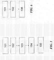
- the figure 1 represents the different steps of the method according to a first embodiment of the present invention.
- Step 101 corresponds to the reception of optical signals. These signals can be of two types, NRZ type signals on the one hand and RZ type signals on the other hand.
- Step 102 corresponds to the optical demodulation of the signals. This step converts the optical signals into binary electrical signals.
- An exemplary embodiment of a demodulation circuit 1 enabling this step (102) is represented on the figure 2 .
- the received optical signal 3 is sent on an optical filter 5 and then transmitted to a photodiode 7.
- the latter is connected on the one hand to ground by a load resistor 6 and on the other hand to a voltage potential V which allows converting the optical signal into an electrical signal.
- the latter is transmitted to a capacitor 15 and then to an electrical amplifier 17.
- the electrical signal is transmitted on the one hand to a clock recovery module 9 and on the other hand to a data channel.
- Said data channel comprises, respectively, a low-low filter 19 and a flip-flop 21. This latter converts the received signal into a binary signal 23 as a function of the clock period 11 coming from the clock recovery module 9 and the predetermined switching threshold 13 for defining the state of the bits transmitted according to the level of the received signal.
- the clock recovery module 9 must be adapted to the signal according to the type of modulation and the signal flow.
- An idea of the present invention is to use a common clock recovery module for two different types of signals.
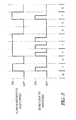
- the figure 3 represents a sequence of binary signals coded on the one hand in the NRZ format and on the other hand in the RZ format. Note that for signals of equivalent frequency, the period of the high signal is twice as low for a signal RZ.
- an idea of the present invention is to use a common demodulation circuit for modulated NRZ signals at a certain rate (X Gb / s) and modulated RZ signals at a rate that is twice as slow as that of NRZ signals ( X / 2 Gb / s).
- a RZ signal has a larger spectral width that a NRZ type signal having the same rate.
- this spectral width is proportional to the flow rate.
- an NRZ signal at a certain rate (10 Gb / s for example) and a signal RZ whose rate is half the rate of the NRZ signal (5Gb / s in the present example) will have the same spectral width.
- the spectral line to be recovered by the module of Clock recovery will be at the same spot of the frequency spectrum. Indeed, for a 10 Gb / s NRZ signal, there is no 10 GHz line in the frequency spectrum of the received signals, but there is a 5 GHz line. At the level of the clock recovery module 9, therefore, the line at 5 GHz is recovered and this frequency is multiplied by two to obtain the clock signal 11. On the other hand, for a signal RZ at 10 Gb / s, there is a line at 10 GHz in the frequency spectrum.
- the present invention therefore makes it possible to use a common demodulation module for two types of signals having different data rates. Nevertheless, the binary signal obtained at the output of the demodulation circuit 1 in the case of a signal RZ whose bit rate is half of the NRZ signal comprises additional bits with respect to the initial binary signal (ie before modulation and transmission). Indeed, by using the same clock recovery module 9, the demodulation creates low level bits corresponding to the second part (low level) of the periods of a signal RZ.
- the signal obtained at the output of the demodulation module 1 in the case of the RZ signals at 5 Gb / s is a signal of 10 Gb / s of which one bit in two is a low level bit added to the initial signal during the demodulation (due to oversampling created by the demodulation module 1).
- every other bit must be extracted, ie deleted, of the binary signal in order to obtain the desired signal.
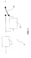
- the signals are transmitted to a first input of a switch 25 on the one hand and to an extraction module 27 whose output is connected to the second input of said switch 25 on the other hand as shown on the figure 5 .
- said figure 5 represents the signal processing device 2 according to the present invention.
- the extraction module 27 can be produced, for example, by a subsampling box for converting a 10 Gb / s signal from a 5 Gb / s RZ signal into a 5 Gb / s signal corresponding to initial signal, ie before demodulation (thus by subsampling, it eliminates the added bits by oversampling performed during the demodulation).
- the switch 25 is positioned by default on one of the two positions (direct transmission for example, ie corresponding to the NRZ signals) (step 103).
- the decoding of the FEC error corrector (step 104) is then analyzed to determine if the positioning of the switch 25 corresponds to the type of signals received. Indeed if the decoder FEC (not shown) is set to a reception mode corresponding to a type of signal (NRZ 10Gb / s for example) while it receives the other type of signals (RZ 5 Gb / s in this example), the bit error rate (BER) measured will be very bad.
- the switch 25 and the decoder FEC will then be switched to the other reception mode (step 105) corresponding to the other type of signals. If the obtained BER is much better, the type of signals corresponding to the second reception mode will be retained.
- the switch 25 will be controlled by a control interface connected to a decoding module FEC.
- the steps of which are represented on the figure 6 (Since steps 101 and 102 are common to the first embodiment described above), the information corresponding to the type of transmitted signals (NRZ at 10 Gb / s or RZ at 5 Gb / s) is transmitted by the management layer of the network at the time the resource reservation is made along the transmission path.
- the type of the received signals is already known and the switch 25 can be positioned according to the information sent by the network management layer (step 106).
- bit extraction can also be performed at the software level on a digital signal obtained from the binary signals transmitted at the output of the demodulation module.
- bit extraction can also be performed at the software level on a digital signal obtained from the binary signals transmitted at the output of the demodulation module.
- the present invention allows from a NRZ type signal processing device to a certain rate, to process RZ type signals at a rate that is twice as low simply by adding an extraction module and by controlling a switch according to the type of signals received.
- the fact of being able to process signals having different bit rates thus makes it possible to adapt the bit rate of the transmitted signals according to the quality required for the signals at the level of the receiver and thus to allow a greater modularity of the network without having to modify in a significant way the equipment of said network.
Landscapes
- Physics & Mathematics (AREA)
- Electromagnetism (AREA)
- Engineering & Computer Science (AREA)
- Computer Networks & Wireless Communication (AREA)
- Signal Processing (AREA)
- Optical Communication System (AREA)
Abstract
- une étape (102) de démodulation transformant un signal reçu modulé selon un type Non Retour à Zéro (NRZ) ou selon un type Retour à Zéro (RZ) en un signal binaire indépendamment du type de modulation;
- si le type de modulation correspond à une modulation de type Retour à Zéro (RZ), une étape supplémentaire d'extraction de certains bits du signal binaire spécifique au type de modulation Retour à Zéro (RZ).
Description
- La présente invention concerne le domaine des réseaux de communication optique et plus particulièrement la démodulation optique des signaux dans ces réseaux.
Afin d'accroître les performances des réseaux de communication optique, de nombreux efforts ont été réalisés récemment afin de développer des transmissions transparentes, c'est à dire, ne nécessitant ni conversion ni régénération du signal optique du noeud source jusqu'au noeud de destination. Lors de ces transmissions transparentes, le signal optique subit des dégradations dans les différents éléments du réseau. Ainsi, la qualité du signal à destination peut-être inférieure à la qualité requise, la transmission étant alors impossible. Plusieurs paramètres peuvent influencer cette dégradation et notamment le débit des signaux. En effet, un signal modulé avec un débit plus faible subira moins de dégradations. Ainsi, un des moyens pour permettre d'utiliser de façon optimale un réseau transparent est d'adapter le débit du signal transmis en fonction de la qualité du signal à destination. Néanmoins, cela nécessite l'emploi au niveau des émetteurs et des récepteurs optiques de composants adaptables à différents débits ce qui implique un gros investissement, notamment à l'échelle d'un réseau. En effet, notamment au niveau de la démodulation des signaux, le traitement de signaux ayant des formats ou des taux de modulation différents impliquent un module de récupération d'horloge adapté pour chaque format et/ou débit. - C'est donc un objet de la présente invention de surmonter ces inconvénients précités de l'état de la technique et de fournir un procédé facile à mettre en oeuvre et peu coûteux pour adapter le débit d'un signal optique en fonction de la qualité du signal désirée à destination.
- A cet effet, l'invention concerne un procédé de traitement de signaux transmis, dans un réseau de communication optique, vers un récepteur par un émetteur apte à transmettre des signaux modulés selon un type Non Retour à Zéro (NRZ) à un premier débit et selon un type Retour à Zéro (RZ) à un second débit, le premier débit étant un multiple du second débit, ledit procédé comprenant au niveau du récepteur les étapes suivantes:
- une étape de démodulation transformant un signal reçu modulé selon un type Non Retour à Zéro (NRZ) ou selon un type Retour à Zéro (RZ) en un signal binaire indépendamment du type de modulation;
- si le type de modulation correspond à une modulation de type Retour à Zéro (RZ), une étape supplémentaire d'extraction de certains bits du signal binaire spécifique au type de modulation Retour à Zéro (RZ).
- Selon un autre mode de réalisation, le premier débit est le double du second débit.
- Selon un mode de réalisation additionnel, l'étape d'extraction de certains bits du signal binaire spécifique au type de modulation Retour à Zéro (RZ) correspond à une suppression d'un bit sur deux et est réalisée par un sous-échantillonnage.
- Selon un autre mode de réalisation, l'étape d'extraction de certains bits du signal binaire spécifique au type de modulation Retour à Zéro (RZ) correspond à une suppression de certains bits du signal et est réalisée au niveau logiciel.
- Selon un mode de réalisation supplémentaire, afin de déterminer le type de signaux reçus, on analyse le taux d'erreur de bits (BER) au niveau du décodage du correcteur d'erreur de type FEC (Forward Error Correction).
- Selon un mode de réalisation additionnel, l'information correspondant au type de signaux reçus est transmise par la couche de gestion du réseau.
- L'invention concerne également un programme d'ordinateur pour traiter des signaux transmis, dans un réseau de communication optique, vers un récepteur par un émetteur apte à transmettre des signaux modulés selon un type Non Retour à Zéro (NRZ) à un premier débit et selon un type Retour à Zéro (RZ) à un second débit, le premier débit étant un multiple du second débit, ledit programme d'ordinateur comprenant des instructions pour la mise en oeuvre des étapes suivantes:
- une étape de démodulation transformant un signal reçu modulé selon un type Non Retour à Zéro (NRZ) ou selon un type Retour à Zéro (RZ) en un signal binaire indépendamment du type de modulation;
- si le type de modulation correspond à une modulation de type Retour à Zéro (RZ), une étape supplémentaire d'extraction de certains bits du signal binaire spécifique au type de modulation Retour à Zéro (RZ).
- Selon un autre mode de réalisation, ledit programme d'ordinateur comprend des instructions pour la mise en oeuvre d'une étape d'analyse du taux d'erreur de bits (BER) au niveau du décodage du correcteur d'erreur de type FEC (Forward Error Correction) afin de déterminer le type de signaux reçus.
- Selon un mode de réalisation supplémentaire, ledit programme d'ordinateur comprend des instructions pour la mise en oeuvre d'une étape de réception et de traitement d'une information envoyée par la couche de gestion du réseau.
- La présente invention concerne également un dispositif de traitement de signaux transmis, dans un réseau de communication optique, vers un récepteur par un émetteur apte à transmettre des signaux modulés selon un type Non Retour à Zéro (NRZ) à un premier débit et selon un type Retour à Zéro (RZ) à un second débit, le premier débit étant un multiple du second débit, ledit dispositif comprenant les moyens pour:
- recevoir un signal modulé selon un type Non Retour à Zéro (NRZ) ou selon un type Retour à Zéro (RZ);
- démoduler un signal modulé reçu en un signal binaire indépendamment du type de modulation;
- extraire certains bits du signal binaire correspondant à un signal de modulation de type Retour à Zéro (RZ).
- Selon un autre mode de réalisation, les moyens de démodulation transformant un signal reçu modulé selon un type Non Retour à Zéro (NRZ) ou selon un type Retour à Zéro (RZ) en un signal binaire comprennent un module de récupération d'horloge et sont communs pour les deux types de modulation.
- Selon un mode de réalisation additionnel, ledit dispositif comprend des moyens de détermination d'au moins un paramètre correspondant au type de modulation du signal reçu;
- Selon un mode de réalisation additionnel, les moyens de détermination d'au moins un paramètre correspondant au type de modulation du signal reçu sont des moyens d'analyse du taux d'erreur de bits (BER) au niveau du décodage du correcteur d'erreur de type FEC (Forward Error Correction).
- Selon un mode de réalisation supplémentaire, les moyens de détermination d'au moins un paramètre correspondant au type de modulation du signal reçu sont des moyens de réception et de traitement d'une information envoyée par la couche de gestion du réseau.
- D'autres caractéristiques et avantages de l'invention apparaîtront dans la description qui va maintenant en être faite, en référence aux dessins annexés qui en représentent, à titre indicatif mais non limitatif, un mode de réalisation possible.
- Sur ces dessins:
- la
figure 1 représente un schéma synoptique des différentes étapes de l'invention selon un premier mode de réalisation; - la
figure 2 représente un schéma d'un démodulateur optique; - la
figure 3 est un schéma représentant les différences entre un signal de type Retour à Zéro (RZ) et un signal de type Non Retour à Zéro (NRZ); - la
figure 4 représente la densité spectrale de trois type de signaux; - la
figure 5 représente un schéma d'un récepteur optique selon la présente invention; - la
figure 6 représente un schéma synoptique des différentes étapes de l'invention selon un deuxième mode de réalisation; - Le terme « RZ » correspond à l'acronyme Retour à Zéro;
- Le terme « NRZ » correspond à l'acronyme Non Retour à Zéro;
- Le terme « FEC » correspond à l'acronyme anglais Forward Error Correction.
- Une idée de la présente invention est de permettre la démodulation de deux types de signaux différents à partir d'un module initialement prévu pour un seul type de signaux en ajoutant simplement un module d'extraction au circuit de démodulation initial.
Afin de réduire les dégradations physiques subies par un signal lors de sa transmission dans un réseau optique, deux solutions peuvent être envisagées.
D'une part, le format de modulation peut être modifié, en passant, par exemple, d'une modulation de type NRZ à une modulation de type RZ. Néanmoins, l'amélioration de la qualité des signaux à destination grâce à une telle modification n'est que très faible.
D'autre part, le débit des signaux peut être modifié, en passant par exemple d'un signal de type NRZ modulé à X Gb/s à un signal de type NRZ modulé à X/2 Gb/s. Dans ce cas, l'amélioration de la qualité des signaux à destination est notable mais cela requiert un module de récupération d'horloge qui s'adapte aux deux débits.
Ainsi, afin de minimiser les modifications nécessaires, au niveau du récepteur, pour démoduler des signaux à des débits différents, la présente invention repose sur l'utilisation des signaux de type NRZ modulés à X Gb/s d'une part et des signaux de type RZ modulés à X/2 Gb/s d'autre part. En effet, les caractéristiques techniques de ces deux types de signaux, qui seront présentées dans la suite de la description, permettent à l'aide de modifications minimes au niveau du récepteur de démoduler des signaux ayant des débits différents. - La
figure 1 représente les différentes étapes du procédé selon un premier mode de réalisation de la présente invention. L'étape 101 correspond à la réception de signaux optiques. Ces signaux peuvent être de deux types, des signaux de type NRZ d'une part et des signaux de type RZ d'autre part. L'étape 102 correspond à la démodulation optique des signaux. Cette étape permet de convertir les signaux optiques en signaux électriques binaires.
Un exemple de réalisation d'un circuit de démodulation 1 permettant cette étape (102) est représenté sur lafigure 2 . Le signal optique reçu 3 est envoyé sur un filtre optique 5 puis transmis à une photodiode 7. Cette dernière est reliée d'une part à la masse par une résistance de charge 6 et d'autre part à un potentiel de tension V ce qui permet la conversion du signal optique en un signal électrique. Ce dernier est transmis à un condensateur 15 puis à un amplificateur électrique 17. En sortie dudit amplificateur 17, le signal électrique est transmis d'une part à un module de récupération d'horloge 9 et d'autre part vers une voie de données. Ladite voie de données comprend, respectivement, un filtre basse-bas 19 et une bascule 21. Cette dernière convertit le signal reçu en un signal binaire 23 en fonction de la période d'horloge 11 issue du module de récupération d'horloge 9 et du seuil de bascule prédéterminé 13 permettant de définir l'état des bits transmis en fonction du niveau du signal reçu.
Néanmoins, le module de récupération d'horloge 9 doit être adapté au signal en fonction du type de modulation et du débit du signal.
Une idée de la présente invention est d'utiliser un module de récupération d'horloge commun pour deux types de signaux différents.
Lafigure 3 représente une séquence de signaux binaire codés d'une part au format NRZ et d'autre part au format RZ. On remarque que pour des signaux de fréquence équivalente, la période du signal haut est deux fois plus faible pour un signal RZ.
Ainsi, une idée de la présente invention est d'utiliser un circuit de démodulation commun pour des signaux NRZ modulés à un certain débit (X Gb/s) et des signaux RZ modulés à un débit deux fois plus faible que celui de signaux NRZ (X/2 Gb/s).
Au niveau de la densité spectrale de puissance (DSP) représentée sur lafigure 4 pour différents signaux (un signal NRZ de 10 Gb/s (a), un signal RZ de 10 Gb/s (b) et un signal RZ de 5 Gb/s (c)), un signal de type RZ a une plus grande largeur spectrale qu'un signal de type NRZ ayant le même débit. De plus, cette largeur spectrale est proportionnelle au débit.
Donc, un signal NRZ à un certain débit (10 Gb/s par exemple) et un signal RZ dont le débit est la moitié du débit du signal NRZ (5Gb/s dans le présent exemple) auront la même largeur spectrale. D'autre part, pour les deux types de signaux, la raie spectrale à récupérer par le module de récupération d'horloge sera au même endroit du spectre de fréquence. En effet, pour un signal NRZ à 10 Gb/s, il n'y a pas de raie à 10 GHz dans le spectre de fréquence des signaux reçus, mais il y a une raie à 5 GHz. Au niveau du module de récupération d'horloge 9, on récupère donc la raie se trouvant à 5 GHz et on multiplie cette fréquence par deux pour obtenir le signal d'horloge 11. Par contre, pour un signal RZ à 10 Gb/s, il y a bien une raie à 10 GHz dans le spectre de fréquence. Ainsi, pour un signal NRZ à X Gb/s et signal RZ à X/2 Gb/s, il y aura une raie à X/2 GHz dans le spectre de fréquence qui permettra de récupérer la fréquence d'horloge 11.
La présente invention permet donc d'utiliser un module de démodulation commun pour deux types de signaux ayant des débits différents.
Néanmoins, le signal binaire obtenu en sortie du circuit de démodulation 1 dans le cas d'un signal RZ dont le débit est la moitié du signal NRZ comprend des bits supplémentaires par rapport au signal binaire initial (i.e. avant modulation et transmission). En effet, en utilisant le même module de récupération d'horloge 9, la démodulation crée des bits de niveau bas correspondant à la deuxième partie (niveau bas) des périodes d'un signal RZ. Le signal obtenu, en sortie du module de démodulation 1 dans le cas des signaux RZ à 5 Gb/s, est un signal de 10 Gb/s dont un bit sur deux est un bit de niveau bas ajouté au signal initial lors de la démodulation (dû au sur-échantillonnage créépar le module de démodulation 1).
Ainsi, dans le cas d'un signal RZun bit sur deux doit être extrait, c'est à dire supprimé, du signal binaire afin d'obtenir le signal désiré.
A la sortie du circuit de démodulation 1, les signaux sont transmis vers une première entrée d'un interrupteur 25 d'une part et vers un module d'extraction 27 dont la sortie est reliée à la deuxième entrée dudit interrupteur 25 d'autre part, tel que représenté sur lafigure 5 . Laditefigure 5 représente le dispositif de traitement des signaux 2 selon la présente invention. Le module d'extraction 27 peut être réalisé, par exemple, par un boîtier de sous-échantillonnage permettant de convertir un signal à 10 Gb/s issu d'un signal RZ à 5Gb/s en un signal à 5 Gb/s correspondant au signal initial, c'est à dire avant démodulation (ainsi en sous-échantillonnant, on élimine les bits ajoutés par le sur-échantillonnage réalisé lors de la démodulation). - L'interrupteur 25 est positionné par défaut sur l'une des deux positions (transmission directe par exemple, c'est à dire correspondant aux signaux NRZ) (étape 103).
On analyse ensuite le décodage du correcteur d'erreur de type FEC (étape 104) afin de déterminer si le positionnement de l'interrupteur 25 correspond bien au type de signaux reçus. En effet si le décodeur FEC (non représenté) est calé sur un mode de réception correspondant à un type de signaux (NRZ à 10Gb/s par exemple) alors qu'il reçoit l'autre type de signaux (RZ à 5 Gb/s dans le présent exemple), le taux d'erreur de bits (BER) mesuré sera très mauvais. L'interrupteur 25 ainsi que le décodeur FEC seront alors commutés sur l'autre mode de réception (étape 105) correspondant à l'autre type de signaux. Si le BER obtenu est largement meilleur, le type de signaux correspondant au deuxième mode de réception sera retenu. Ainsi l'interrupteur 25 sera piloté par une interface de commande reliée à un module de décodage FEC. - Selon un deuxième mode de réalisation dont les étapes sont représentées sur la
figure 6 (les étapes 101 et 102 étant communes avec le premier mode de réalisation décrit précédemment), l'information correspondant au type de signaux transmis (NRZ à 10 Gb/s ou RZ à 5 Gb/s) est transmise par la couche de gestion du réseau au moment où est faite la réservation des ressources le long du chemin de transmission. Ainsi, au moment de la réception des signaux au niveau du circuit de démodulation 1, le type des signaux reçus est déjà connu et l'interrupteur 25 peut être positionné en fonction de l'information envoyée par la couche de gestion du réseau (étape 106). - Par ailleurs, les différentes étapes de l'invention, telles que décrites précédemment et pour les deux modes de réalisation, peuvent être gérées par un programme d'ordinateur.
- D'autre part, dans un mode de réalisation alternatif, l'extraction des bits peut également être réalisée au niveau logiciel sur un signal numérique obtenu à partir des signaux binaires transmis en sortie du module de démodulation. Dans ce cas, pour obtenir le signal désiré, on peut soit extraire les bits utiles du signal pour les transmettre, soit extraire du signal les bits à supprimer et transmettre les bits restants.
- Ainsi la présente invention permet à partir d'un dispositif de traitement de signaux de type NRZ à un certain débit, de traiter des signaux de type RZ à un débit deux fois plus faible en ajoutant simplement un module d'extraction et en pilotant un interrupteur en fonction du type de signaux reçus. Le fait de pouvoir traiter des signaux ayant des débits différents permet donc d'adapter le débit des signaux transmis en fonction de la qualité requise pour les signaux au niveau du récepteur et permettre ainsi une plus grande modularité du réseau sans avoir à modifier de façon importante les équipements dudit réseau.
Claims (14)
- Procédé de traitement de signaux transmis, dans un réseau de communication optique, vers un récepteur par un émetteur apte à transmettre des signaux modulés selon un type Non Retour à Zéro (NRZ) à un premier débit et selon un type Retour à Zéro (RZ) à un second débit, le premier débit étant un multiple du second débit, ledit procédé comprenant au niveau du récepteur les étapes suivantes:- une étape (102) de démodulation transformant un signal reçu modulé selon un type Non Retour à Zéro (NRZ) ou selon un type Retour à Zéro (RZ) en un signal binaire indépendamment du type de modulation;- si le type de modulation correspond à une modulation de type Retour à Zéro (RZ), une étape supplémentaire d'extraction de certains bits du signal binaire spécifique au type de modulation Retour à Zéro (RZ).
- Procédé de traitement de signaux selon la revendication 1 dans lequel le premier débit est le double du second débit.
- Procédé de traitement de signaux selon la revendication 2 dans lequel l'étape d'extraction de certains bits du signal binaire spécifique au type de modulation Retour à Zéro (RZ) correspond à une suppression d'un bit sur deux et est réalisée par un sous-échantillonnage.
- Procédé de traitement de signaux selon la revendication 1 ou 2 dans lequel l'étape d'extraction de certains bits du signal binaire spécifique au type de modulation Retour à Zéro (RZ) correspond à une suppression de certains bits du signal et est réalisée au niveau logiciel.
- Procédé de traitement de signaux selon l'une des revendications précédentes dans lequel afin de déterminer le type de signaux reçus, on analyse le taux d'erreur de bits (BER) au niveau du décodage du correcteur d'erreur de type FEC (Forward Error Correction).
- Procédé de traitement de signaux selon l'une des revendications 1 à 4 dans lequel l'information correspondant au type de signaux reçus est transmise par la couche de gestion du réseau.
- Programme d'ordinateur pour traiter des signaux transmis, dans un réseau de communication optique, vers un récepteur par un émetteur apte à transmettre des signaux modulés selon un type Non Retour à Zéro (NRZ) à un premier débit et selon un type Retour à Zéro (RZ) à un second débit, le premier débit étant un multiple du second débit, ledit programme d'ordinateur comprenant des instructions pour la mise en oeuvre des étapes suivantes:- une étape de démodulation (102) transformant un signal reçu modulé selon un type Non Retour à Zéro (NRZ) ou selon un type Retour à Zéro (RZ) en un signal binaire indépendamment du type de modulation;- si le type de modulation correspond à une modulation de type Retour à Zéro (RZ), une étape supplémentaire d'extraction de certains bits du signal binaire spécifique au type de modulation Retour à Zéro (RZ).
- Programme d'ordinateur selon la revendication 7 comprenant des instructions pour la mise en oeuvre d'une étape d'analyse du taux d'erreur de bits (BER) au niveau du décodage du correcteur d'erreur de type FEC (Forward Error Correction) afin de déterminer le type de signaux reçus.
- Programme d'ordinateur selon la revendication 7 comprenant des instructions pour la mise en oeuvre d'une étape de réception et de traitement d'une information envoyée par la couche de gestion du réseau.
- Dispositif de traitement de signaux transmis, dans un réseau de communication optique, vers un récepteur par un émetteur apte à transmettre des signaux modulés selon un type Non Retour à Zéro (NRZ) à un premier débit et selon un type Retour à Zéro (RZ) à un second débit, le premier débit étant un multiple du second débit, ledit dispositif comprenant les moyens pour:- recevoir un signal modulé selon un type Non Retour à Zéro (NRZ) ou selon un type Retour à Zéro (RZ);- démoduler un signal modulé reçu en un signal binaire indépendamment du type de modulation;- extraire certains bits du signal binaire correspondant à un signal de modulation de type Retour à Zéro (RZ).
- Dispositif de traitement de signaux selon la revendication 10 dans lequel les moyens de démodulation transformant un signal reçu modulé selon un type Non Retour à Zéro (NRZ) ou selon un type Retour à Zéro (RZ) en un signal binaire comprennent un module de récupération d'horloge (9) et sont communs pour les deux types de modulation.
- Dispositif de traitement de signaux selon la revendication 10 ou 11 comprenant également:- des moyens de détermination d'au moins un paramètre correspondant au type de modulation du signal reçu;
- Dispositif de traitement de signaux selon la revendication 12 dans lequel les moyens de détermination d'au moins un paramètre correspondant au type de modulation du signal reçu sont des moyens d'analyse du taux d'erreur de bits (BER) au niveau du décodage du correcteur d'erreur de type FEC (Forward Error Correction).
- Dispositif de traitement de signaux selon la revendication 12 dans lequel les moyens de détermination d'au moins un paramètre correspondant au type de modulation du signal reçu sont des moyens de réception et de traitement d'une information envoyée par la couche de gestion du réseau.
Applications Claiming Priority (1)
| Application Number | Priority Date | Filing Date | Title |
|---|---|---|---|
| FR0900110A FR2941109B1 (fr) | 2009-01-12 | 2009-01-12 | Procede et equipement de traitement de signaux dans un reseau optique de communication |
Publications (2)
| Publication Number | Publication Date |
|---|---|
| EP2207281A1 true EP2207281A1 (fr) | 2010-07-14 |
| EP2207281B1 EP2207281B1 (fr) | 2013-03-20 |
Family
ID=40910996
Family Applications (1)
| Application Number | Title | Priority Date | Filing Date |
|---|---|---|---|
| EP20100150120 Active EP2207281B1 (fr) | 2009-01-12 | 2010-01-05 | Procédé et équipement de traitement de signaux dans un réseau optique de communication |
Country Status (2)
| Country | Link |
|---|---|
| EP (1) | EP2207281B1 (fr) |
| FR (1) | FR2941109B1 (fr) |
Citations (2)
| Publication number | Priority date | Publication date | Assignee | Title |
|---|---|---|---|---|
| JP2003092553A (ja) * | 2000-09-19 | 2003-03-28 | Fujitsu Ltd | 光通信システム及び光受信器 |
| US20060233555A1 (en) * | 2005-04-19 | 2006-10-19 | Jae-Myoung Lee | Apparatus for optical clock extraction |
-
2009
- 2009-01-12 FR FR0900110A patent/FR2941109B1/fr not_active Expired - Fee Related
-
2010
- 2010-01-05 EP EP20100150120 patent/EP2207281B1/fr active Active
Patent Citations (2)
| Publication number | Priority date | Publication date | Assignee | Title |
|---|---|---|---|---|
| JP2003092553A (ja) * | 2000-09-19 | 2003-03-28 | Fujitsu Ltd | 光通信システム及び光受信器 |
| US20060233555A1 (en) * | 2005-04-19 | 2006-10-19 | Jae-Myoung Lee | Apparatus for optical clock extraction |
Non-Patent Citations (1)
| Title |
|---|
| WEIMING MAO ET AL: "All-Optical Clock Recovery for Both RZ and NRZ Data", IEEE PHOTONICS TECHNOLOGY LETTERS, IEEE SERVICE CENTER, PISCATAWAY, NJ, US, vol. 14, no. 6, 1 June 2002 (2002-06-01), XP011067151, ISSN: 1041-1135 * |
Also Published As
| Publication number | Publication date |
|---|---|
| FR2941109B1 (fr) | 2010-12-31 |
| EP2207281B1 (fr) | 2013-03-20 |
| FR2941109A1 (fr) | 2010-07-16 |
Similar Documents
| Publication | Publication Date | Title |
|---|---|---|
| US10142092B2 (en) | Optical transceiver and method with channel binding, clock forwarding, and integrate-and-dump receivers | |
| US8873968B2 (en) | Optical field receiver, optical multilevel signal receiver, and optical transmission system | |
| US9755763B2 (en) | Adaptive post digital filter and inter-symbol interference equalizer for optical communication | |
| US8571407B2 (en) | Optical coherent receiver, apparatus for and method of monitoring performance thereof | |
| US9722698B2 (en) | Channel performance monitoring and an optical communication system using same | |
| Zhou et al. | Advanced DSP for 400 Gb/s and beyond optical networks | |
| US11025405B2 (en) | High capacity optical data transmission using intensity-modulation and direct-detection | |
| FR2546008A1 (fr) | Circuit d'egalisation adaptative et de demodulation conjointes | |
| JP5888056B2 (ja) | デジタル光コヒーレント伝送装置 | |
| WO2015027903A1 (fr) | Communication optique utilisant des signaux super-nyquist | |
| JP5316736B1 (ja) | デジタル受信機及び波形補償方法 | |
| EP3857809B1 (fr) | Extraction d'horloge dans des systèmes affectés par une forte interférence entre symboles | |
| EP4068713B1 (fr) | Procédé d'égalisation de domaine fréquentiel, égaliseur, récepteur optique et système | |
| JP6636884B2 (ja) | 光送信機、光伝送システム及び光受信機 | |
| US20080199191A1 (en) | Maximum likelihood sequence estimation for high spectral efficiency optical communication systems | |
| US10826615B2 (en) | Optical transmission method and optical receiver apparatus for determining received symbols from a received electrical signal using an indication of a nonlinear impulse response of the direct detection and without performing equalization following the direct detection | |
| FR2955222A1 (fr) | Procede de recuperation d'un signal | |
| EP2207281B1 (fr) | Procédé et équipement de traitement de signaux dans un réseau optique de communication | |
| FR3093877A1 (fr) | Méthode de modulation numérique d’ordre élevé robuste au bruit de phase | |
| CA2781137C (fr) | Systeme et procede d'emission-reception d'un signal numerique sur voie radio | |
| Li et al. | Effect of bandwidth narrowing due to cascaded wavelength selective switches on the generalized mutual information of probabilistically shaped 64-QAM systems | |
| JP2020108115A (ja) | 光通信装置、サーバ装置、光伝送システム、及び光通信方法 | |
| US7474860B2 (en) | Optimum sample spacing in over-sampled maximum likelihood sequence estimation receivers | |
| FR3016262A1 (fr) | Pre-distorsion d'un signal optique a sous-porteuses multiplexees en frequence | |
| CN110463082B (zh) | 具有受控比特概率的传输系统 |
Legal Events
| Date | Code | Title | Description |
|---|---|---|---|
| PUAI | Public reference made under article 153(3) epc to a published international application that has entered the european phase |
Free format text: ORIGINAL CODE: 0009012 |
|
| AK | Designated contracting states |
Kind code of ref document: A1 Designated state(s): AT BE BG CH CY CZ DE DK EE ES FI FR GB GR HR HU IE IS IT LI LT LU LV MC MK MT NL NO PL PT RO SE SI SK SM TR |
|
| AX | Request for extension of the european patent |
Extension state: AL BA RS |
|
| 17P | Request for examination filed |
Effective date: 20110114 |
|
| 17Q | First examination report despatched |
Effective date: 20110208 |
|
| RAP1 | Party data changed (applicant data changed or rights of an application transferred) |
Owner name: ALCATEL LUCENT |
|
| GRAP | Despatch of communication of intention to grant a patent |
Free format text: ORIGINAL CODE: EPIDOSNIGR1 |
|
| GRAS | Grant fee paid |
Free format text: ORIGINAL CODE: EPIDOSNIGR3 |
|
| REG | Reference to a national code |
Ref country code: DE Ref legal event code: R079 Ref document number: 602010005514 Country of ref document: DE Free format text: PREVIOUS MAIN CLASS: H04B0010158000 Ipc: H04B0010660000 |
|
| GRAA | (expected) grant |
Free format text: ORIGINAL CODE: 0009210 |
|
| RIC1 | Information provided on ipc code assigned before grant |
Ipc: H04B 10/66 20130101AFI20130204BHEP |
|
| AK | Designated contracting states |
Kind code of ref document: B1 Designated state(s): AT BE BG CH CY CZ DE DK EE ES FI FR GB GR HR HU IE IS IT LI LT LU LV MC MK MT NL NO PL PT RO SE SI SK SM TR |
|
| REG | Reference to a national code |
Ref country code: GB Ref legal event code: FG4D Free format text: NOT ENGLISH |
|
| REG | Reference to a national code |
Ref country code: CH Ref legal event code: EP |
|
| REG | Reference to a national code |
Ref country code: IE Ref legal event code: FG4D Free format text: LANGUAGE OF EP DOCUMENT: FRENCH |
|
| REG | Reference to a national code |
Ref country code: AT Ref legal event code: REF Ref document number: 602610 Country of ref document: AT Kind code of ref document: T Effective date: 20130415 |
|
| REG | Reference to a national code |
Ref country code: DE Ref legal event code: R096 Ref document number: 602010005514 Country of ref document: DE Effective date: 20130516 |
|
| PG25 | Lapsed in a contracting state [announced via postgrant information from national office to epo] |
Ref country code: BG Free format text: LAPSE BECAUSE OF FAILURE TO SUBMIT A TRANSLATION OF THE DESCRIPTION OR TO PAY THE FEE WITHIN THE PRESCRIBED TIME-LIMIT Effective date: 20130620 Ref country code: SE Free format text: LAPSE BECAUSE OF FAILURE TO SUBMIT A TRANSLATION OF THE DESCRIPTION OR TO PAY THE FEE WITHIN THE PRESCRIBED TIME-LIMIT Effective date: 20130320 Ref country code: NO Free format text: LAPSE BECAUSE OF FAILURE TO SUBMIT A TRANSLATION OF THE DESCRIPTION OR TO PAY THE FEE WITHIN THE PRESCRIBED TIME-LIMIT Effective date: 20130620 Ref country code: LT Free format text: LAPSE BECAUSE OF FAILURE TO SUBMIT A TRANSLATION OF THE DESCRIPTION OR TO PAY THE FEE WITHIN THE PRESCRIBED TIME-LIMIT Effective date: 20130320 Ref country code: ES Free format text: LAPSE BECAUSE OF FAILURE TO SUBMIT A TRANSLATION OF THE DESCRIPTION OR TO PAY THE FEE WITHIN THE PRESCRIBED TIME-LIMIT Effective date: 20130701 |
|
| REG | Reference to a national code |
Ref country code: AT Ref legal event code: MK05 Ref document number: 602610 Country of ref document: AT Kind code of ref document: T Effective date: 20130320 |
|
| REG | Reference to a national code |
Ref country code: LT Ref legal event code: MG4D |
|
| PG25 | Lapsed in a contracting state [announced via postgrant information from national office to epo] |
Ref country code: FI Free format text: LAPSE BECAUSE OF FAILURE TO SUBMIT A TRANSLATION OF THE DESCRIPTION OR TO PAY THE FEE WITHIN THE PRESCRIBED TIME-LIMIT Effective date: 20130320 Ref country code: LV Free format text: LAPSE BECAUSE OF FAILURE TO SUBMIT A TRANSLATION OF THE DESCRIPTION OR TO PAY THE FEE WITHIN THE PRESCRIBED TIME-LIMIT Effective date: 20130320 Ref country code: SI Free format text: LAPSE BECAUSE OF FAILURE TO SUBMIT A TRANSLATION OF THE DESCRIPTION OR TO PAY THE FEE WITHIN THE PRESCRIBED TIME-LIMIT Effective date: 20130320 Ref country code: GR Free format text: LAPSE BECAUSE OF FAILURE TO SUBMIT A TRANSLATION OF THE DESCRIPTION OR TO PAY THE FEE WITHIN THE PRESCRIBED TIME-LIMIT Effective date: 20130621 |
|
| REG | Reference to a national code |
Ref country code: NL Ref legal event code: VDEP Effective date: 20130320 |
|
| PG25 | Lapsed in a contracting state [announced via postgrant information from national office to epo] |
Ref country code: HR Free format text: LAPSE BECAUSE OF FAILURE TO SUBMIT A TRANSLATION OF THE DESCRIPTION OR TO PAY THE FEE WITHIN THE PRESCRIBED TIME-LIMIT Effective date: 20130320 |
|
| PG25 | Lapsed in a contracting state [announced via postgrant information from national office to epo] |
Ref country code: RO Free format text: LAPSE BECAUSE OF FAILURE TO SUBMIT A TRANSLATION OF THE DESCRIPTION OR TO PAY THE FEE WITHIN THE PRESCRIBED TIME-LIMIT Effective date: 20130320 Ref country code: EE Free format text: LAPSE BECAUSE OF FAILURE TO SUBMIT A TRANSLATION OF THE DESCRIPTION OR TO PAY THE FEE WITHIN THE PRESCRIBED TIME-LIMIT Effective date: 20130320 Ref country code: NL Free format text: LAPSE BECAUSE OF FAILURE TO SUBMIT A TRANSLATION OF THE DESCRIPTION OR TO PAY THE FEE WITHIN THE PRESCRIBED TIME-LIMIT Effective date: 20130320 Ref country code: AT Free format text: LAPSE BECAUSE OF FAILURE TO SUBMIT A TRANSLATION OF THE DESCRIPTION OR TO PAY THE FEE WITHIN THE PRESCRIBED TIME-LIMIT Effective date: 20130320 Ref country code: IS Free format text: LAPSE BECAUSE OF FAILURE TO SUBMIT A TRANSLATION OF THE DESCRIPTION OR TO PAY THE FEE WITHIN THE PRESCRIBED TIME-LIMIT Effective date: 20130720 Ref country code: CZ Free format text: LAPSE BECAUSE OF FAILURE TO SUBMIT A TRANSLATION OF THE DESCRIPTION OR TO PAY THE FEE WITHIN THE PRESCRIBED TIME-LIMIT Effective date: 20130320 Ref country code: PT Free format text: LAPSE BECAUSE OF FAILURE TO SUBMIT A TRANSLATION OF THE DESCRIPTION OR TO PAY THE FEE WITHIN THE PRESCRIBED TIME-LIMIT Effective date: 20130722 Ref country code: SK Free format text: LAPSE BECAUSE OF FAILURE TO SUBMIT A TRANSLATION OF THE DESCRIPTION OR TO PAY THE FEE WITHIN THE PRESCRIBED TIME-LIMIT Effective date: 20130320 |
|
| PG25 | Lapsed in a contracting state [announced via postgrant information from national office to epo] |
Ref country code: PL Free format text: LAPSE BECAUSE OF FAILURE TO SUBMIT A TRANSLATION OF THE DESCRIPTION OR TO PAY THE FEE WITHIN THE PRESCRIBED TIME-LIMIT Effective date: 20130320 Ref country code: CY Free format text: LAPSE BECAUSE OF FAILURE TO SUBMIT A TRANSLATION OF THE DESCRIPTION OR TO PAY THE FEE WITHIN THE PRESCRIBED TIME-LIMIT Effective date: 20130320 |
|
| PLBE | No opposition filed within time limit |
Free format text: ORIGINAL CODE: 0009261 |
|
| STAA | Information on the status of an ep patent application or granted ep patent |
Free format text: STATUS: NO OPPOSITION FILED WITHIN TIME LIMIT |
|
| PG25 | Lapsed in a contracting state [announced via postgrant information from national office to epo] |
Ref country code: DK Free format text: LAPSE BECAUSE OF FAILURE TO SUBMIT A TRANSLATION OF THE DESCRIPTION OR TO PAY THE FEE WITHIN THE PRESCRIBED TIME-LIMIT Effective date: 20130320 |
|
| 26N | No opposition filed |
Effective date: 20140102 |
|
| PG25 | Lapsed in a contracting state [announced via postgrant information from national office to epo] |
Ref country code: IT Free format text: LAPSE BECAUSE OF FAILURE TO SUBMIT A TRANSLATION OF THE DESCRIPTION OR TO PAY THE FEE WITHIN THE PRESCRIBED TIME-LIMIT Effective date: 20130320 |
|
| REG | Reference to a national code |
Ref country code: DE Ref legal event code: R097 Ref document number: 602010005514 Country of ref document: DE Effective date: 20140102 |
|
| BERE | Be: lapsed |
Owner name: ALCATEL LUCENT Effective date: 20140131 |
|
| REG | Reference to a national code |
Ref country code: CH Ref legal event code: PCOW Free format text: NEW ADDRESS: 148/152 ROUTE DE LA REINE, 92100 BOULOGNE-BILLANCOURT (FR) |
|
| PG25 | Lapsed in a contracting state [announced via postgrant information from national office to epo] |
Ref country code: LU Free format text: LAPSE BECAUSE OF FAILURE TO SUBMIT A TRANSLATION OF THE DESCRIPTION OR TO PAY THE FEE WITHIN THE PRESCRIBED TIME-LIMIT Effective date: 20140105 Ref country code: MC Free format text: LAPSE BECAUSE OF FAILURE TO SUBMIT A TRANSLATION OF THE DESCRIPTION OR TO PAY THE FEE WITHIN THE PRESCRIBED TIME-LIMIT Effective date: 20130320 |
|
| REG | Reference to a national code |
Ref country code: CH Ref legal event code: PL |
|
| PG25 | Lapsed in a contracting state [announced via postgrant information from national office to epo] |
Ref country code: CH Free format text: LAPSE BECAUSE OF NON-PAYMENT OF DUE FEES Effective date: 20140131 Ref country code: LI Free format text: LAPSE BECAUSE OF NON-PAYMENT OF DUE FEES Effective date: 20140131 |
|
| REG | Reference to a national code |
Ref country code: IE Ref legal event code: MM4A |
|
| REG | Reference to a national code |
Ref country code: FR Ref legal event code: PLFP Year of fee payment: 6 |
|
| PG25 | Lapsed in a contracting state [announced via postgrant information from national office to epo] |
Ref country code: IE Free format text: LAPSE BECAUSE OF NON-PAYMENT OF DUE FEES Effective date: 20140105 Ref country code: BE Free format text: LAPSE BECAUSE OF NON-PAYMENT OF DUE FEES Effective date: 20140131 |
|
| REG | Reference to a national code |
Ref country code: FR Ref legal event code: PLFP Year of fee payment: 7 |
|
| PG25 | Lapsed in a contracting state [announced via postgrant information from national office to epo] |
Ref country code: MT Free format text: LAPSE BECAUSE OF FAILURE TO SUBMIT A TRANSLATION OF THE DESCRIPTION OR TO PAY THE FEE WITHIN THE PRESCRIBED TIME-LIMIT Effective date: 20130320 |
|
| PG25 | Lapsed in a contracting state [announced via postgrant information from national office to epo] |
Ref country code: SM Free format text: LAPSE BECAUSE OF FAILURE TO SUBMIT A TRANSLATION OF THE DESCRIPTION OR TO PAY THE FEE WITHIN THE PRESCRIBED TIME-LIMIT Effective date: 20130320 |
|
| PG25 | Lapsed in a contracting state [announced via postgrant information from national office to epo] |
Ref country code: HU Free format text: LAPSE BECAUSE OF FAILURE TO SUBMIT A TRANSLATION OF THE DESCRIPTION OR TO PAY THE FEE WITHIN THE PRESCRIBED TIME-LIMIT; INVALID AB INITIO Effective date: 20100105 Ref country code: TR Free format text: LAPSE BECAUSE OF FAILURE TO SUBMIT A TRANSLATION OF THE DESCRIPTION OR TO PAY THE FEE WITHIN THE PRESCRIBED TIME-LIMIT Effective date: 20130320 |
|
| REG | Reference to a national code |
Ref country code: FR Ref legal event code: PLFP Year of fee payment: 8 |
|
| REG | Reference to a national code |
Ref country code: FR Ref legal event code: PLFP Year of fee payment: 9 |
|
| PG25 | Lapsed in a contracting state [announced via postgrant information from national office to epo] |
Ref country code: MK Free format text: LAPSE BECAUSE OF FAILURE TO SUBMIT A TRANSLATION OF THE DESCRIPTION OR TO PAY THE FEE WITHIN THE PRESCRIBED TIME-LIMIT Effective date: 20130320 |
|
| REG | Reference to a national code |
Ref country code: DE Ref legal event code: R082 Ref document number: 602010005514 Country of ref document: DE Representative=s name: METACOM LEGAL RECHTSANWAELTE, DE Ref country code: DE Ref legal event code: R082 Ref document number: 602010005514 Country of ref document: DE Representative=s name: METACOM LEGAL, DE Ref country code: DE Ref legal event code: R081 Ref document number: 602010005514 Country of ref document: DE Owner name: WSOU INVESTMENTS, LLC, LOS ANGELES, US Free format text: FORMER OWNER: ALCATEL LUCENT, PARIS, FR Ref country code: DE Ref legal event code: R082 Ref document number: 602010005514 Country of ref document: DE Representative=s name: BARKHOFF REIMANN VOSSIUS, DE |
|
| REG | Reference to a national code |
Ref country code: GB Ref legal event code: 732E Free format text: REGISTERED BETWEEN 20200924 AND 20200930 |
|
| REG | Reference to a national code |
Ref country code: DE Ref legal event code: R082 Ref document number: 602010005514 Country of ref document: DE Representative=s name: METACOM LEGAL RECHTSANWAELTE, DE Ref country code: DE Ref legal event code: R082 Ref document number: 602010005514 Country of ref document: DE Representative=s name: METACOM LEGAL, DE Ref country code: DE Ref legal event code: R082 Ref document number: 602010005514 Country of ref document: DE Representative=s name: METACOM LEGAL NAGEL MARKOWSKY VOSSIUS RECHTSAN, DE |
|
| P01 | Opt-out of the competence of the unified patent court (upc) registered |
Effective date: 20230606 |
|
| PGFP | Annual fee paid to national office [announced via postgrant information from national office to epo] |
Ref country code: DE Payment date: 20250627 Year of fee payment: 16 |
|
| PGFP | Annual fee paid to national office [announced via postgrant information from national office to epo] |
Ref country code: GB Payment date: 20250627 Year of fee payment: 16 |
|
| PGFP | Annual fee paid to national office [announced via postgrant information from national office to epo] |
Ref country code: FR Payment date: 20250625 Year of fee payment: 16 |