EP2207206A1 - Organic light emitting display device and method of manufacturing the same - Google Patents
Organic light emitting display device and method of manufacturing the same Download PDFInfo
- Publication number
- EP2207206A1 EP2207206A1 EP10150419A EP10150419A EP2207206A1 EP 2207206 A1 EP2207206 A1 EP 2207206A1 EP 10150419 A EP10150419 A EP 10150419A EP 10150419 A EP10150419 A EP 10150419A EP 2207206 A1 EP2207206 A1 EP 2207206A1
- Authority
- EP
- European Patent Office
- Prior art keywords
- oxide semiconductor
- semiconductor layer
- light emitting
- organic light
- layer
- Prior art date
- Legal status (The legal status is an assumption and is not a legal conclusion. Google has not performed a legal analysis and makes no representation as to the accuracy of the status listed.)
- Granted
Links
Images



Classifications
-
- H—ELECTRICITY
- H10—SEMICONDUCTOR DEVICES; ELECTRIC SOLID-STATE DEVICES NOT OTHERWISE PROVIDED FOR
- H10K—ORGANIC ELECTRIC SOLID-STATE DEVICES
- H10K59/00—Integrated devices, or assemblies of multiple devices, comprising at least one organic light-emitting element covered by group H10K50/00
- H10K59/10—OLED displays
- H10K59/12—Active-matrix OLED [AMOLED] displays
- H10K59/121—Active-matrix OLED [AMOLED] displays characterised by the geometry or disposition of pixel elements
- H10K59/1213—Active-matrix OLED [AMOLED] displays characterised by the geometry or disposition of pixel elements the pixel elements being TFTs
-
- H—ELECTRICITY
- H10—SEMICONDUCTOR DEVICES; ELECTRIC SOLID-STATE DEVICES NOT OTHERWISE PROVIDED FOR
- H10D—INORGANIC ELECTRIC SEMICONDUCTOR DEVICES
- H10D86/00—Integrated devices formed in or on insulating or conducting substrates, e.g. formed in silicon-on-insulator [SOI] substrates or on stainless steel or glass substrates
- H10D86/40—Integrated devices formed in or on insulating or conducting substrates, e.g. formed in silicon-on-insulator [SOI] substrates or on stainless steel or glass substrates characterised by multiple TFTs
- H10D86/421—Integrated devices formed in or on insulating or conducting substrates, e.g. formed in silicon-on-insulator [SOI] substrates or on stainless steel or glass substrates characterised by multiple TFTs having a particular composition, shape or crystalline structure of the active layer
- H10D86/423—Integrated devices formed in or on insulating or conducting substrates, e.g. formed in silicon-on-insulator [SOI] substrates or on stainless steel or glass substrates characterised by multiple TFTs having a particular composition, shape or crystalline structure of the active layer comprising semiconductor materials not belonging to the Group IV, e.g. InGaZnO
-
- H—ELECTRICITY
- H10—SEMICONDUCTOR DEVICES; ELECTRIC SOLID-STATE DEVICES NOT OTHERWISE PROVIDED FOR
- H10D—INORGANIC ELECTRIC SEMICONDUCTOR DEVICES
- H10D86/00—Integrated devices formed in or on insulating or conducting substrates, e.g. formed in silicon-on-insulator [SOI] substrates or on stainless steel or glass substrates
- H10D86/40—Integrated devices formed in or on insulating or conducting substrates, e.g. formed in silicon-on-insulator [SOI] substrates or on stainless steel or glass substrates characterised by multiple TFTs
- H10D86/421—Integrated devices formed in or on insulating or conducting substrates, e.g. formed in silicon-on-insulator [SOI] substrates or on stainless steel or glass substrates characterised by multiple TFTs having a particular composition, shape or crystalline structure of the active layer
- H10D86/425—Integrated devices formed in or on insulating or conducting substrates, e.g. formed in silicon-on-insulator [SOI] substrates or on stainless steel or glass substrates characterised by multiple TFTs having a particular composition, shape or crystalline structure of the active layer having different crystal properties in different TFTs or within an individual TFT
-
- H—ELECTRICITY
- H10—SEMICONDUCTOR DEVICES; ELECTRIC SOLID-STATE DEVICES NOT OTHERWISE PROVIDED FOR
- H10D—INORGANIC ELECTRIC SEMICONDUCTOR DEVICES
- H10D86/00—Integrated devices formed in or on insulating or conducting substrates, e.g. formed in silicon-on-insulator [SOI] substrates or on stainless steel or glass substrates
- H10D86/40—Integrated devices formed in or on insulating or conducting substrates, e.g. formed in silicon-on-insulator [SOI] substrates or on stainless steel or glass substrates characterised by multiple TFTs
- H10D86/60—Integrated devices formed in or on insulating or conducting substrates, e.g. formed in silicon-on-insulator [SOI] substrates or on stainless steel or glass substrates characterised by multiple TFTs wherein the TFTs are in active matrices
-
- H—ELECTRICITY
- H10—SEMICONDUCTOR DEVICES; ELECTRIC SOLID-STATE DEVICES NOT OTHERWISE PROVIDED FOR
- H10K—ORGANIC ELECTRIC SOLID-STATE DEVICES
- H10K2102/00—Constructional details relating to the organic devices covered by this subclass
- H10K2102/10—Transparent electrodes, e.g. using graphene
- H10K2102/101—Transparent electrodes, e.g. using graphene comprising transparent conductive oxides [TCO]
Definitions
- the present invention relates to an organic light emitting display device and a method of manufacturing the same, and more particularly, to an organic light emitting display device that has a difference in charge mobility between a thin film transistor of a drive unit and a thin film transistor of a pixel unit, and a method of manufacturing the same.
- An organic light emitting display device is a next generation display device which may actively emit light. Compared to a liquid crystal display device (LCD), the organic light emitting display device has excellent characteristics in terms of viewing angle, contrast, response speed, power consumption, and other related functional properties.
- LCD liquid crystal display device
- An organic light emitting display device generally includes an organic light emitting diode that has an anode electrode, an organic light emitting layer, and a cathode electrode.
- the organic light emitting display device may be divided into a passive matrix type where the organic light emitting diode is connected between scan lines and signal lines in a matrix type to constitute a pixel, and an active matrix type where the operations of each pixel are controlled by a thin film transistor (TFT) that functions as a switch.
- TFT thin film transistor
- an activation layer provides source and drain regions, and a channel region.
- the activation layer is generally formed of a semiconductor layer made of amorphous silicon, poly-silicon, low temperature poly-silicon (LTPS), or other similar material.
- the amorphous silicon has a low mobility, therefore, the amorphous silicon is difficult to be implemented in a driving circuit which operates at a high speed. Therefore, the activation layer is generally made of the poly-silicon or the low temperature poly-silicon that has a high charge mobility compared to the amorphous silicon.
- the poly-silicon has a disadvantage that threshold voltage is uneven due to the nature of polycrystalline, and the low temperature poly-silicon has a disadvantage that a laser annealing or other related processs for crystallization may be required during the manufacture of the poly-silicon.
- Japanese Laid-Open Patent Publication No. 2004-273614 discloses a thin film transistor which has zinc oxide (ZnO) or an oxide semiconductor having zinc oxide (ZnO) as a main ingredient, as an activation layer.
- Amorphous InGaZnO Indium-Gallium-Zinc oxide; hereinafter, referred to as IGZO
- IGZO Indium-Gallium-Zinc oxide
- the amorphous IGZO is however insufficient for being used as the activation layer of the thin film transistor of the drive unit where a high charge mobility (about 100cm 2 /V ⁇ sec) at a level of the low temperature poly-silicon is required.
- an organic light emitting display device including: a substrate that includes a first region (preferably non-pixel region) and a second region (preferably pixel region); a first thin film transistor that includes a gate electrode formed in the first region on the substrate, an activation layer insulated from the gate electrode by a gate insulating layer and the activation layer formed in a structure where a first semiconductor layer and a second semiconductor layer are stacked, and source and drain electrodes electrically and physically coupled to the activation layer, with the first oxide semiconductor layer having a carrier concentration higher than the second oxide semiconductor layer; a second thin film transistor that includes a gate electrode formed in the second region on the substrate, an activation layer insulated from the gate electrode by a gate insulating layer and formed of the second oxide semiconductor layer, and source and drain electrodes electrically and physically coupled to the activation layer; an insulating layer that is formed on the second thin film transistor and has a via hole in order that the source or drain electrode of the second thin film
- the gate insulating layer of the first thin film transistor is the same layer as the gate insulating layer of the second thin film transistor.
- the first region is a drive unit.
- the first oxide semiconductor layer is formed between the second oxide semiconductor layer and the gate insulating layer.
- the first oxide semiconductor layer is selected from a group consisting of ITO, InZnO, InSnO, AlZnO, AlGaO and InGaO.
- the first oxide semiconductor layer is formed to be thinner than the second oxide semiconductor layer.
- the first oxide semiconductor layer is formed with a thickness of 1 to 5 nm, more preferably the first oxide semiconductor layer is formed with a thickness of 2 to 4 nm.
- the second oxide semiconductor layer comprises zinc oxide (ZnO).
- the second oxide semiconductor layer is doped with at least one ion selected from gallium (Ga), indium (In), stannum (Sn), zirconium (Zr), hafnium (Hf), cadmium (Cd), silver (Ag), copper (Cu), germanium (Ge), gadolinium (Gd), and vanadium (V).
- the second oxide semiconductor layer is formed with a thickness of 10 to 50 nm, more preferably the second oxide semiconductor layer is formed with a thickness of 20 to 40 nm.
- the first oxide semiconductor layer has a carrier concentration of 1e+19#/cm 3 to 1e+21#/cm 3 , more preferably the first oxide semiconductor layer has a carrier concentration of 5*10 ⁇ 19#/cm 3 to 5*10 ⁇ 20#/cm 3 .
- the second oxide semiconductor layer has a carrier concentration of 1e+13#/cm 3 to 1e+18#/cm 3 . More preferably the second oxide semiconductor layer has a carrier concentration of 1e+14#/cm 3 to 1e+17#/cm 3 .
- 1e+18#/cm 3 means 10 18 (10 ⁇ 18) charge carriers per cm 3 .
- the expression "carrier concentration" of a layer is understood as a charge carrier concentration of the layer when no voltage (i.e. no electric field) is applied to the layer.
- an organic light emitting display device (the organic light emitting display device according to at least one of the above disclosed features, respectively), including steps of: preparing a substrate that includes a first region and a second region; forming gate electrodes of first and second thin film transistors respectively disposed in the first and second regions on the substrate; forming a gate insulating layer on the gate electrodes in the first and second regions; forming an activation layer formed in a structure where a first semiconductor layer and a second semiconductor layer are stacked on the gate insulating layer in the first region, the first oxide semiconductor layer having a carrier concentration higher than the second oxide semiconductor layer, and forming an activation layer formed of the second oxide semiconductor layer on the gate insulating layer in the second region; forming source and drain electrodes to be electrically and physically coupled to the activation layer in the first and second regions, respectively; forming an insulating layer on the second thin film transistor and then forming a via hole in order that the source or drain electrode of the second
- the first region is a drive unit.
- the first oxide semiconductor layer made of at least one material selected from a group consisting of ITO, InZnO, InSnO, AlZnO, AlGaO and InGaO.
- the first oxide semiconductor layer is formed to be thinner than the second oxide semiconductor layer.
- the first oxide semiconductor layer is formed with a thickness of 1 to 5 nm.
- the second oxide semiconductor layer comprises zinc oxide (ZnO).
- the second oxide semiconductor layer is doped with at least one ion selected from gallium (Ga), indium (In), stannum (Sn), zirconium (Zr), hafnium (Hf), cadmium (Cd), silver (Ag), copper (Cu), germanium (Ge), gadolinium (Gd), and vanadium (V).
- the forming the activation layer comprises: forming the first oxide semiconductor layer on the gate insulating layer in the first and second regions; patterning the first oxide semiconductor layer; forming the second oxide semiconductor layer in the first and second regions in which the first oxide semiconductor layer is included; and patterning the second semiconductor layer in the first and second regions.
- an organic light emitting display device including the thin film transistor of the drive unit that has the activation layer formed in a structure where the first oxide semiconductor layer and the second oxide semiconductor layer are stacked, the thin film transistor of the pixel unit that has the activation layer formed of the second oxide semiconductor layer, and the organic light emitting diode physically coupled to the thin film transistor of the pixel unit.
- the thin film transistor of the drive unit has a channel formed on the first oxide semiconductor layer having a higher carrier concentration than the second oxide semiconductor layer, having a high charge mobility.
- the thin film transistor of the pixel unit has a channel formed on the second oxide semiconductor layer, so that the thin film transistor of the pixel unit has a stable and uniform functional property.
- an organic light emitting display device comprising: a first thin film transistor disposed on a non-pixel region of a substrate, the first thin film transistor comprising a first activation layer formed by a first semiconductor layer and a second semiconductor layer which are disposed in immediate physical contact with each other, with the first oxide semiconductor layer having a different value of carrier concentration compared to that of the second oxide semiconductor layer; a second thin film transistor disposed on a pixel region of the substrate, the second thin film transistor having a second activation layer formed of one of the first and second oxide semiconductor layers.
- the first oxide semiconductor layer has a higher value of the carrier concentration compared to that of the second oxide semiconductor layer.
- the second activation layer is formed of the second oxide semiconductor layer.
- FIGS. 1A and 1B are respectively a plan view and a cross-sectional view explaining an organic light emitting display device in accordance with the present invention.
- a substrate 100 includes a pixel region 140 and a non-pixel region 150.
- Non-pixel region 150 becomes a region surrounding pixel region 140 or a region other than pixel region 140.
- Scan lines 142 and data lines 144 are formed in the pixel region 140 disposed on the substrate 100, and are intersected with each other.
- a plurality of pixel units 146 are disposed and coupled between scan lines 142 and data lines 144 in a matrix arrangement.
- the pixel unit 146 may include an organic light emitting diode, a thin film transistor that controls the operation of the organic light emitting diode, and a capacitor that maintains signals at a predetermined level.
- Scan lines 142 and data lines 144 are extended from pixel region 140 to non-pixel region 150.
- a power supply line (not shown) operates the organic light emitting diode
- a scan drive unit 160 and a data drive unit 170 process signals provided from the exterior through a pad 180 in order to supply external signals to scan lines 142 and data lines 144, e.g. external signals containing video data or the like.
- Scan drive unit 160 and data drive unit 170 include a driving circuit that converts the external signals through pad 180 into the scan signals and data signals in order to selectively drive each of the pixels.
- a sealing substrate 200 that seals pixel region 140 is disposed, and sealing substrate 200 is bonded to substrate 100 by means of a sealant 300 that is disposed to surround pixel region 140.
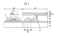
- FIG. 2 is a cross-sectional view more specifically explaining the structures of pixel unit 146 and scan drive unit 160 of FIG. 1A .
- pixel unit 146 shows only a thin film transistor 120 and an organic light emitting diode 130
- scan drive unit 160 shows only a thin film transistor 110.
- scan drive unit 160 is shown, however a thin film transistor of a data drive unit 170 has the same structure. It shall be understood that each of pixel unit 146 and scan drive unit 160 may comprise more than one transistor.
- a buffer layer 101 is formed on substrate 100 in both of pixel region 140 and non-pixel region 150.
- pixel region 140 exemplarily shows pixel unit 146
- non-pixel region 150 exemplarily shows scan drive unit 160.
- Thin film transistor 110 that forms the driving circuit is formed on buffer layer 101 of scan drive unit 160, and a thin film transistor 120 that functions as a switch is formed on buffer layer 101 of pixel unit 146.
- Thin film transistor 110 of scan drive unit 160 includes a gate electrode 111, an activation layer 112 insulated from gate electrode 111 by a gate insulating layer 102, and source and drain electrodes 113 electrically and physically coupled to activation layer 112 in source and drain regions.
- Activation layer 112 is formed in a structure where semiconductor layers having different carrier concentrations (different conductivities) are stacked, more specifically, in a structure where a first oxide semiconductor layer 112a having a high carrier concentration and a second oxide semiconductor layer 112b having a carrier concentration lower than that of the first oxide semiconductor layer 112a are stacked.
- a thickness of a portion where a channel is substantially formed (for example, a thickness of about 1nm to 5 nm) is formed of the first oxide semiconductor layer 112a having a relatively higher carrier concentration (1e+19 to 1e+21#/cm 3 ) (herein # represents the number of carriers), and a thickness of most portions other than the portion where a channel is substantially formed (for example, a thickness of about 10 to 50 nm) is formed of the second oxide semiconductor layer 112b having a relatively lower carrier concentration (1e+13 to 1e+18#/cm 3 ).
- the first oxide semiconductor layer 112a may be selected from a group consisting of Indium-tin oxide (ITO), InZnO (IZO), InSnO, AlZnO, AlGaO and InGaO
- the second oxide semiconductor layer 112b may be formed of zinc oxide (ZnO) or zinc oxide (ZnO) doped with one ion selected from gallium (Ga), indium (In), stannum (Sn), zirconium (Zr), hafnium (Hf), cadmium (Cd), silver (Ag), copper (Cu), germanium (Ge), gadolinium (Gd), and vanadium (V), for example, ZnO, ZnSnO, and InGaZnO, etc., ITO and IZO, etc., are commonly used as a conductive layer, however, these materials may have semiconductor properties when the carrier concentration thereof is controlled by controlling the thickness to be thin and controlling the oxygen concentration during the deposition process.
- thin film transistor 120 of pixel unit 146 includes gate electrode 121, activation layer 122 insulated from gate electrode 121 by gate insulating layer 102, and source and drain electrodes 123 electrically and physically coupled to activation layer 122 in the source and drain regions, wherein activation layer 122 is formed of an oxide semiconductor having the same layer or the same material as the second oxide semiconductor layer 112b that constitutes activation layer 112 of thin film transistor 110.
- activation layer 122 may be formed of zinc oxide (ZnO) or zinc oxide (ZnO) doped with one ion selected from gallium (Ga), indium (In), stannum (Sn), zirconium (Zr), hafnium (Hf), cadmium (Cd), silver (Ag), copper (Cu), germanium (Ge), gadolinium (Gd), and vanadium (V), for example, ZnO, ZnSnO, and InGaZnO, etc.
- an insulating layer 103 is formed for planarization on thin film transistor 120 of pixel unit 146, and a via hole is formed on insulating layer 103 in order that source or drain electrodes 123 of thin film transistor 120 are exposed.
- An organic light emitting diode 130 is formed on insulating layer 103 of pixel unit 146 to be electrically coupled to one of source and drain electrodes 123 of thin film transistor 120 through the via hole.
- Organic light emitting diode 130 includes an anode electrode 131 that is electrically coupled to one of source and drain electrodes 123 of thin film transistor 120 through the via hole, an organic light emitting layer 133 formed on anode electrode 131 in a light emitting region exposed by a pixel definition layer 132, and a cathode electrode 134 formed on pixel definition layer 132 that includes organic light emitting layer 133.
- Organic light emitting layer 133 may include a hole injection layer, a hole transport layer, an electron transport layer, and an electron injection layer.
- activation layer 122 of thin film transistor 120 of pixel unit 146 is formed of the oxide semiconductor layer identified above, and activation layer 112 of thin film transistor 110 of drive units 160 and 170 is formed in a structure where the first oxide semiconductor layer 112a and the second oxide semiconductor layer 112b, having different carrier concentrations (i.e., having different conductivities), are stacked.
- activation layer 122 of thin film transistor 120 of pixel unit 146 where relatively low charge mobility (10 to 20 cm 2 /V ⁇ sec) and high property uniformity are required is formed of the oxide semiconductor layer made of ZnO, InGaZnO, InSnZnO and ZnSnO, etc.; and activation layer 112 of thin film transistor 110 of drive units 160 and 170, where a relatively high charge mobility (50 to 130 cm 2 /V ⁇ sec) is required, is formed of the first oxide semiconductor layer 112a made of ITO and IZO, etc.
- thin film transistor 110 of drive units 160 and 170 has a channel formed on the first oxide semiconductor layer 112a having a higher carrier concentration than that of the second oxide semiconductor layer 112b so that thin film transistor 110 has a high charge mobility; and thin film transistor 120 of pixel unit 146 has a channel formed on the second oxide semiconductor layer 122 so that thin film transistor 120 has a stable and even property.
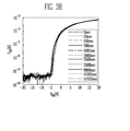
- FIGS. 3A through 3C are two dimensional graphs showing the change in current I DS between the drain electrode and the source electrode according to the change in voltage V GS applied between the gate electrode and the source electrode.
- FIG. 3A shows thin film transistor 110 of drive unit 160 that has activation layer 112 made of InZnO 112a and GaInZnO 112b;
- FIG. 3B shows thin film transistor 110 of drive unit 160 that has activation layer 112 made of ITO 112a and GaInZnO 112b;
- FIG. 3C shows thin film transistor 110 of pixel unit 146 that has activation layer 122 made of GaInZnO. It can be appreciated that when the size of device is the same, the thin film transistor of drive unit 160 of FIGS. 3A and 3B is more excellent on current property compared to thin film transistor 120 of the pixel unit 146 of FIG. 3C , resulted from the difference in charge mobility of the oxide semiconductor layers.
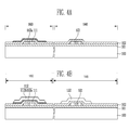
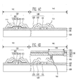
- FIGS. 4A through 4D are cross-sectional views showing a method of manufacturing an organic light emitting display device in accordance with the present invention.
- a substrate 100 defined with a pixel region 140 and a non-pixel region 150 is prepared.
- pixel region 140 shows a pixel unit 146
- non-pixel region 150 shows a scan drive unit 160.
- a buffer layer 101 is formed on substrate 100 in pixel region 140 and non-pixel region 150, and gate electrodes 111 and 121 of thin film transistors 110 and 120 are formed on the buffer layer of scan driver unit 160 and pixel unit 146, respectively.
- Gate insulating layer 102 and the first oxide semiconductor layer 112a are sequentially formed on the entire gate electrodes 111 and 121. Then the first oxide semiconductor layer 112a is patterned, thereby maintaining the first oxide semiconductor layer 112a only disposed on gate insulating layer 102 of scan drive unit 160.
- the first oxide semiconductor layer 112a is formed by depositing ITO, IZO, InSnO, AlZnO, AlGaO, and InGaO at a thickness of 1nm to 5nm.
- the second oxide semiconductor layer 112b is formed on the entire upper portion in which the first oxide semiconductor layer 112a is included, and then is patterned. Therefore, activation layer 112 is formed in a stacked structure of the first oxide semiconductor layer 112a and the second oxide semiconductor layer 112b in scan drive unit 160. Simultaneously, activation layer 122 is formed of the same layer as the second oxide semiconductor layer 112b in pixel unit 146.
- the second oxide semiconductor layer 112b is made of ZnO, ZnSnO and InGaZnO, etc.
- a conductive layer is formed on the entire upper portion in which activation layers 112 and 122 are included and is then patterned, thereby forming source and drain electrodes 113 and 123 electrically coupled to the source and drain regions of activation layers 112 and 122, respectively.
- insulating layer 103 is formed in order that the upper portion, in which thin film transistors 110 and 120 are included or the upper portion in which the thin film transistor 120 is included, is planarized. Then via hole 190 is formed in order that one of source and drain electrodes 123 of thin film transistor 120 is exposed. On insulating layer 103 of pixel unit 146, anode electrode 131, that is electrically coupled to one of source and drain electrode 123 of thin film transistor 120 through via hole 190, is formed.
- Opening part 192 is formed on anode electrode 131 in order that anode electrode 131 in the light emitting region is exposed by forming and patterning pixel definition layer 132; and organic light emitting layer 133 is formed on the anode electrode of the opening part.
- Organic light emitting layer 133 may include a hole injection layer, a hole transport layer, an electron transport layer and an electron injection layer.
- cathode electrode 134 is formed on pixel definition layer 132 including organic light emitting layer 133, thereby forming organic light emitting diode 130.
Landscapes
- Physics & Mathematics (AREA)
- Geometry (AREA)
- Engineering & Computer Science (AREA)
- Microelectronics & Electronic Packaging (AREA)
- Electroluminescent Light Sources (AREA)
- Devices For Indicating Variable Information By Combining Individual Elements (AREA)
- Thin Film Transistor (AREA)
- Shift Register Type Memory (AREA)
Abstract
Description
- This application makes reference to, incorporates the same herein, and claims priority and all benefits from the patent application filed in the Korean Intellectual Property Office on January 12, 2009 and there duly assigned Serial No.
10-2009-0002242 - The present invention relates to an organic light emitting display device and a method of manufacturing the same, and more particularly, to an organic light emitting display device that has a difference in charge mobility between a thin film transistor of a drive unit and a thin film transistor of a pixel unit, and a method of manufacturing the same.
- An organic light emitting display device is a next generation display device which may actively emit light. Compared to a liquid crystal display device (LCD), the organic light emitting display device has excellent characteristics in terms of viewing angle, contrast, response speed, power consumption, and other related functional properties.
- An organic light emitting display device generally includes an organic light emitting diode that has an anode electrode, an organic light emitting layer, and a cathode electrode. The organic light emitting display device may be divided into a passive matrix type where the organic light emitting diode is connected between scan lines and signal lines in a matrix type to constitute a pixel, and an active matrix type where the operations of each pixel are controlled by a thin film transistor (TFT) that functions as a switch.
- In the thin film transistor used in the active matrix type of organic light emitting display device, an activation layer provides source and drain regions, and a channel region. The activation layer is generally formed of a semiconductor layer made of amorphous silicon, poly-silicon, low temperature poly-silicon (LTPS), or other similar material.
- In general, the amorphous silicon has a low mobility, therefore, the amorphous silicon is difficult to be implemented in a driving circuit which operates at a high speed. Therefore, the activation layer is generally made of the poly-silicon or the low temperature poly-silicon that has a high charge mobility compared to the amorphous silicon. However, the poly-silicon has a disadvantage that threshold voltage is uneven due to the nature of polycrystalline, and the low temperature poly-silicon has a disadvantage that a laser annealing or other related processs for crystallization may be required during the manufacture of the poly-silicon.
- Research and study on the oxide semiconductor which may be used as an activation layer have been recently conducted in order to solve the above identified problems.
- Japanese Laid-Open Patent Publication No.
2004-273614 - Amorphous InGaZnO (Indium-Gallium-Zinc oxide; hereinafter, referred to as IGZO) has a charge mobility higher by ten times (about 10cm2/V·sec) compared to the amorphous silicon, and has even property distribution, therefore, the amorphous IGZO is sufficient for being used as the activation layer of the thin film transistor of the pixel unit. The amorphous IGZO is however insufficient for being used as the activation layer of the thin film transistor of the drive unit where a high charge mobility (about 100cm2/V·sec) at a level of the low temperature poly-silicon is required. Furthermore, since the size and the requirement of the resolution of a display device are increased, the amount of data transmitted and the processing speed should be increased, and the most part of a driving circuit should be formed on one substrate in order to reduce the cost of manufacture. Therefore, significant problems may occur in stable property distribution and reliability of the thin film transistor of the drive unit.
- It is therefore an object of the present invention to provide an improved organic light emitting display device that can improve charge mobility of a thin film transistor which uses an oxide semiconductor as an activation layer, and a method of manufacturing the same.
- It is another object of the present invention to provide an organic light emitting display device in which the charge mobility of a thin film transistor of a drive unit is higher than the charge mobility of a thin film transistor of a pixel unit, and a method of manufacturing the same.
- In order to accomplish the above objects, according to one aspect of the present invention, there is provided an organic light emitting display device including: a substrate that includes a first region (preferably non-pixel region) and a second region (preferably pixel region); a first thin film transistor that includes a gate electrode formed in the first region on the substrate, an activation layer insulated from the gate electrode by a gate insulating layer and the activation layer formed in a structure where a first semiconductor layer and a second semiconductor layer are stacked, and source and drain electrodes electrically and physically coupled to the activation layer, with the first oxide semiconductor layer having a carrier concentration higher than the second oxide semiconductor layer; a second thin film transistor that includes a gate electrode formed in the second region on the substrate, an activation layer insulated from the gate electrode by a gate insulating layer and formed of the second oxide semiconductor layer, and source and drain electrodes electrically and physically coupled to the activation layer; an insulating layer that is formed on the second thin film transistor and has a via hole in order that the source or drain electrode of the second thin film transistor is exposed; and an organic light emitting diode that includes a first electrode formed on the insulating layer in the second region and the first electrode electrically and physically coupled to the source or drain electrode of the second thin film transistor through the via hole, an organic light emitting layer formed on the first electrode; and a second electrode formed on the organic light emitting layer.
- Preferably the gate insulating layer of the first thin film transistor is the same layer as the gate insulating layer of the second thin film transistor.
- Preferably the first region is a drive unit. Preferably the first oxide semiconductor layer is formed between the second oxide semiconductor layer and the gate insulating layer. Preferably the first oxide semiconductor layer is selected from a group consisting of ITO, InZnO, InSnO, AlZnO, AlGaO and InGaO. Preferably the first oxide semiconductor layer is formed to be thinner than the second oxide semiconductor layer. Preferably the first oxide semiconductor layer is formed with a thickness of 1 to 5 nm, more preferably the first oxide semiconductor layer is formed with a thickness of 2 to 4 nm. Preferably the second oxide semiconductor layer comprises zinc oxide (ZnO). Preferably the second oxide semiconductor layer is doped with at least one ion selected from gallium (Ga), indium (In), stannum (Sn), zirconium (Zr), hafnium (Hf), cadmium (Cd), silver (Ag), copper (Cu), germanium (Ge), gadolinium (Gd), and vanadium (V). Preferably the second oxide semiconductor layer is formed with a thickness of 10 to 50 nm, more preferably the second oxide semiconductor layer is formed with a thickness of 20 to 40 nm. Preferably the first oxide semiconductor layer has a carrier concentration of 1e+19#/cm3 to 1e+21#/cm3, more preferably the first oxide semiconductor layer has a carrier concentration of 5*10^19#/cm3 to 5*10^20#/cm3. Preferably the second oxide semiconductor layer has a carrier concentration of 1e+13#/cm3 to 1e+18#/cm3. More preferably the second oxide semiconductor layer has a carrier concentration of 1e+14#/cm3 to 1e+17#/cm3. For example, in the present invention 1e+18#/cm3 means 1018 (10^18) charge carriers per cm3. In the present invention, the expression "carrier concentration" of a layer is understood as a charge carrier concentration of the layer when no voltage (i.e. no electric field) is applied to the layer.
- According to another aspect of the present invention, there is provided a method of manufacturing an organic light emitting display device (the organic light emitting display device according to at least one of the above disclosed features, respectively), including steps of: preparing a substrate that includes a first region and a second region; forming gate electrodes of first and second thin film transistors respectively disposed in the first and second regions on the substrate; forming a gate insulating layer on the gate electrodes in the first and second regions; forming an activation layer formed in a structure where a first semiconductor layer and a second semiconductor layer are stacked on the gate insulating layer in the first region, the first oxide semiconductor layer having a carrier concentration higher than the second oxide semiconductor layer, and forming an activation layer formed of the second oxide semiconductor layer on the gate insulating layer in the second region; forming source and drain electrodes to be electrically and physically coupled to the activation layer in the first and second regions, respectively; forming an insulating layer on the second thin film transistor and then forming a via hole in order that the source or drain electrode of the second thin film transistor is exposed; and forming an organic light emitting diode that includes a first electrode formed on the insulating layer in the second region and the first electrode electrically coupled to the source or drain electrode of the second thin film transistor through the via hole, an organic light emitting layer formed on the first electrode; and a second electrode formed on the organic light emitting layer.
- Preferably the first region is a drive unit. Preferably the first oxide semiconductor layer made of at least one material selected from a group consisting of ITO, InZnO, InSnO, AlZnO, AlGaO and InGaO. Preferably the first oxide semiconductor layer is formed to be thinner than the second oxide semiconductor layer. Preferably the first oxide semiconductor layer is formed with a thickness of 1 to 5 nm. Preferably the second oxide semiconductor layer comprises zinc oxide (ZnO). Preferably the second oxide semiconductor layer is doped with at least one ion selected from gallium (Ga), indium (In), stannum (Sn), zirconium (Zr), hafnium (Hf), cadmium (Cd), silver (Ag), copper (Cu), germanium (Ge), gadolinium (Gd), and vanadium (V). Preferably the forming the activation layer comprises: forming the first oxide semiconductor layer on the gate insulating layer in the first and second regions; patterning the first oxide semiconductor layer; forming the second oxide semiconductor layer in the first and second regions in which the first oxide semiconductor layer is included; and patterning the second semiconductor layer in the first and second regions.
- According to another aspect of the present invention, there is provided an organic light emitting display device including the thin film transistor of the drive unit that has the activation layer formed in a structure where the first oxide semiconductor layer and the second oxide semiconductor layer are stacked, the thin film transistor of the pixel unit that has the activation layer formed of the second oxide semiconductor layer, and the organic light emitting diode physically coupled to the thin film transistor of the pixel unit. The thin film transistor of the drive unit has a channel formed on the first oxide semiconductor layer having a higher carrier concentration than the second oxide semiconductor layer, having a high charge mobility. The thin film transistor of the pixel unit has a channel formed on the second oxide semiconductor layer, so that the thin film transistor of the pixel unit has a stable and uniform functional property.
- According to another aspect of the present invention, there is provided an organic light emitting display device, comprising: a first thin film transistor disposed on a non-pixel region of a substrate, the first thin film transistor comprising a first activation layer formed by a first semiconductor layer and a second semiconductor layer which are disposed in immediate physical contact with each other, with the first oxide semiconductor layer having a different value of carrier concentration compared to that of the second oxide semiconductor layer; a second thin film transistor disposed on a pixel region of the substrate, the second thin film transistor having a second activation layer formed of one of the first and second oxide semiconductor layers.
Preferably the first oxide semiconductor layer has a higher value of the carrier concentration compared to that of the second oxide semiconductor layer. Preferably the second activation layer is formed of the second oxide semiconductor layer. - More complete appreciation of the invention, and many of the attendant advantages thereof, will be readily apparent as the same becomes better understood by reference to the following detailed description when considered in conjunction with the accompanying drawings in which like reference symbols indicate the same or similar components, wherein:
-
FIGS. 1A and 1B are respectively a plan view and a cross-sectional view explaining an organic light emitting display device in accordance with the present invention; -
FIG. 2 is a cross-sectional view explaining the structures of a pixel unit and a scan drive unit ofFIG. 1A ; -
FIGS. 3A through 3C are two dimensional graphs showing the change in current IDS between a drain electrode and a source electrode according to the change in voltage VGS applied to a gate electrode and the source electrode ofFIG. 3C ; and -
FIGS. 4A through 4D are cross-sectional views showing a method of manufacturing an organic light emitting display device in accordance with the present invention. - In the following detailed description, only certain exemplary embodiments of the present invention have been shown and described, simply by way of illustration. As those skilled in the art would realize, the described embodiments may be modified in various different ways, all without departing from the scope of the present invention. Accordingly, the drawings and description are to be regarded as illustrative in nature and not restrictive.
- In addition, when an element is referred to as being "on" another element, it can be directly on the other element or be indirectly on the other element with one or more intervening elements interposed therebetween. Also, when an element is referred to as being "connected to" another element, it can be directly connected to the other element or be indirectly connected to the other element with one or more intervening elements interposed therebetween. Further, some of the elements that are not essential to the complete description of the invention have been omitted for clarity. In addition, like reference numerals refer to like elements throughout the description.
- Hereinafter, exemplary embodiments according to the present invention will be described in detail with reference to the accompanying drawings.
-
FIGS. 1A and 1B are respectively a plan view and a cross-sectional view explaining an organic light emitting display device in accordance with the present invention. - Referring to
FIG. 1A , asubstrate 100 includes apixel region 140 and anon-pixel region 150.Non-pixel region 150 becomes a region surroundingpixel region 140 or a region other thanpixel region 140. -
Scan lines 142 anddata lines 144 are formed in thepixel region 140 disposed on thesubstrate 100, and are intersected with each other. In thepixel region 140 disposed on thesubstrate 100, a plurality ofpixel units 146 are disposed and coupled betweenscan lines 142 anddata lines 144 in a matrix arrangement. Thepixel unit 146 may include an organic light emitting diode, a thin film transistor that controls the operation of the organic light emitting diode, and a capacitor that maintains signals at a predetermined level. -
Scan lines 142 anddata lines 144 are extended frompixel region 140 tonon-pixel region 150. Innon-pixel region 150 disposed onsubstrate 100, a power supply line (not shown) operates the organic light emitting diode, and ascan drive unit 160 and adata drive unit 170 process signals provided from the exterior through apad 180 in order to supply external signals to scanlines 142 anddata lines 144, e.g. external signals containing video data or the like.Scan drive unit 160 and data driveunit 170 include a driving circuit that converts the external signals throughpad 180 into the scan signals and data signals in order to selectively drive each of the pixels. - Referring to
FIG. 1B , onsubstrate 100 wherepixel unit 146 is formed, a sealingsubstrate 200 that sealspixel region 140 is disposed, and sealingsubstrate 200 is bonded tosubstrate 100 by means of asealant 300 that is disposed to surroundpixel region 140. -
FIG. 2 is a cross-sectional view more specifically explaining the structures ofpixel unit 146 and scandrive unit 160 ofFIG. 1A . For convenience of explanation,pixel unit 146 shows only athin film transistor 120 and an organiclight emitting diode 130, and scandrive unit 160 shows only athin film transistor 110. In the drawing, only scandrive unit 160 is shown, however a thin film transistor of adata drive unit 170 has the same structure. It shall be understood that each ofpixel unit 146 and scandrive unit 160 may comprise more than one transistor. - Referring to
FIG. 2 , abuffer layer 101 is formed onsubstrate 100 in both ofpixel region 140 andnon-pixel region 150. In the drawing,pixel region 140 exemplarilyshows pixel unit 146, andnon-pixel region 150 exemplarily shows scandrive unit 160. -
Thin film transistor 110 that forms the driving circuit is formed onbuffer layer 101 ofscan drive unit 160, and athin film transistor 120 that functions as a switch is formed onbuffer layer 101 ofpixel unit 146. -
Thin film transistor 110 ofscan drive unit 160 includes agate electrode 111, anactivation layer 112 insulated fromgate electrode 111 by agate insulating layer 102, and source and drainelectrodes 113 electrically and physically coupled toactivation layer 112 in source and drain regions.Activation layer 112 is formed in a structure where semiconductor layers having different carrier concentrations (different conductivities) are stacked, more specifically, in a structure where a firstoxide semiconductor layer 112a having a high carrier concentration and a second oxide semiconductor layer 112b having a carrier concentration lower than that of the firstoxide semiconductor layer 112a are stacked. In other words, a thickness of a portion where a channel is substantially formed (for example, a thickness of about 1nm to 5 nm) is formed of the firstoxide semiconductor layer 112a having a relatively higher carrier concentration (1e+19 to 1e+21#/cm3) (herein # represents the number of carriers), and a thickness of most portions other than the portion where a channel is substantially formed (for example, a thickness of about 10 to 50 nm) is formed of the second oxide semiconductor layer 112b having a relatively lower carrier concentration (1e+13 to 1e+18#/cm3). For example, the firstoxide semiconductor layer 112a may be selected from a group consisting of Indium-tin oxide (ITO), InZnO (IZO), InSnO, AlZnO, AlGaO and InGaO, and the second oxide semiconductor layer 112b may be formed of zinc oxide (ZnO) or zinc oxide (ZnO) doped with one ion selected from gallium (Ga), indium (In), stannum (Sn), zirconium (Zr), hafnium (Hf), cadmium (Cd), silver (Ag), copper (Cu), germanium (Ge), gadolinium (Gd), and vanadium (V), for example, ZnO, ZnSnO, and InGaZnO, etc., ITO and IZO, etc., are commonly used as a conductive layer, however, these materials may have semiconductor properties when the carrier concentration thereof is controlled by controlling the thickness to be thin and controlling the oxygen concentration during the deposition process. - Meanwhile,
thin film transistor 120 ofpixel unit 146 includesgate electrode 121,activation layer 122 insulated fromgate electrode 121 bygate insulating layer 102, and source and drainelectrodes 123 electrically and physically coupled toactivation layer 122 in the source and drain regions, whereinactivation layer 122 is formed of an oxide semiconductor having the same layer or the same material as the second oxide semiconductor layer 112b that constitutesactivation layer 112 ofthin film transistor 110. In other words,activation layer 122 may be formed of zinc oxide (ZnO) or zinc oxide (ZnO) doped with one ion selected from gallium (Ga), indium (In), stannum (Sn), zirconium (Zr), hafnium (Hf), cadmium (Cd), silver (Ag), copper (Cu), germanium (Ge), gadolinium (Gd), and vanadium (V), for example, ZnO, ZnSnO, and InGaZnO, etc.. - Also, an insulating
layer 103 is formed for planarization onthin film transistor 120 ofpixel unit 146, and a via hole is formed on insulatinglayer 103 in order that source or drainelectrodes 123 ofthin film transistor 120 are exposed. An organiclight emitting diode 130 is formed on insulatinglayer 103 ofpixel unit 146 to be electrically coupled to one of source and drainelectrodes 123 ofthin film transistor 120 through the via hole. - Organic
light emitting diode 130 includes ananode electrode 131 that is electrically coupled to one of source and drainelectrodes 123 ofthin film transistor 120 through the via hole, an organiclight emitting layer 133 formed onanode electrode 131 in a light emitting region exposed by apixel definition layer 132, and acathode electrode 134 formed onpixel definition layer 132 that includes organiclight emitting layer 133. Organiclight emitting layer 133 may include a hole injection layer, a hole transport layer, an electron transport layer, and an electron injection layer. - With the present invention constituted as above,
activation layer 122 ofthin film transistor 120 ofpixel unit 146 is formed of the oxide semiconductor layer identified above, andactivation layer 112 ofthin film transistor 110 ofdrive units oxide semiconductor layer 112a and the second oxide semiconductor layer 112b, having different carrier concentrations (i.e., having different conductivities), are stacked. In other words,activation layer 122 ofthin film transistor 120 ofpixel unit 146 where relatively low charge mobility (10 to 20 cm2/V·sec) and high property uniformity are required, is formed of the oxide semiconductor layer made of ZnO, InGaZnO, InSnZnO and ZnSnO, etc.; andactivation layer 112 ofthin film transistor 110 ofdrive units oxide semiconductor layer 112a made of ITO and IZO, etc. having a relatively higher carrier concentration (having a high concentration), and the second oxide semiconductor layer 112b made of ZnO, InGaZnO, InSnZnO and ZnSnO, etc. having a lower carrier concentration (having a low concentration). Therefore,thin film transistor 110 ofdrive units oxide semiconductor layer 112a having a higher carrier concentration than that of the second oxide semiconductor layer 112b so thatthin film transistor 110 has a high charge mobility; andthin film transistor 120 ofpixel unit 146 has a channel formed on the secondoxide semiconductor layer 122 so thatthin film transistor 120 has a stable and even property. -
FIGS. 3A through 3C are two dimensional graphs showing the change in current IDS between the drain electrode and the source electrode according to the change in voltage VGS applied between the gate electrode and the source electrode.FIG. 3A showsthin film transistor 110 ofdrive unit 160 that hasactivation layer 112 made ofInZnO 112a and GaInZnO 112b;FIG. 3B showsthin film transistor 110 ofdrive unit 160 that hasactivation layer 112 made ofITO 112a and GaInZnO 112b; andFIG. 3C showsthin film transistor 110 ofpixel unit 146 that hasactivation layer 122 made of GaInZnO. It can be appreciated that when the size of device is the same, the thin film transistor ofdrive unit 160 ofFIGS. 3A and3B is more excellent on current property compared tothin film transistor 120 of thepixel unit 146 ofFIG. 3C , resulted from the difference in charge mobility of the oxide semiconductor layers. -
FIGS. 4A through 4D are cross-sectional views showing a method of manufacturing an organic light emitting display device in accordance with the present invention. - Referring to
FIG. 4A , asubstrate 100 defined with apixel region 140 and anon-pixel region 150 is prepared. In the drawing,pixel region 140 shows apixel unit 146, andnon-pixel region 150 shows ascan drive unit 160. - A
buffer layer 101 is formed onsubstrate 100 inpixel region 140 andnon-pixel region 150, andgate electrodes thin film transistors scan driver unit 160 andpixel unit 146, respectively. -
Gate insulating layer 102 and the firstoxide semiconductor layer 112a are sequentially formed on theentire gate electrodes oxide semiconductor layer 112a is patterned, thereby maintaining the firstoxide semiconductor layer 112a only disposed ongate insulating layer 102 ofscan drive unit 160. The firstoxide semiconductor layer 112a is formed by depositing ITO, IZO, InSnO, AlZnO, AlGaO, and InGaO at a thickness of 1nm to 5nm. - Referring to
FIG. 4B , the second oxide semiconductor layer 112b is formed on the entire upper portion in which the firstoxide semiconductor layer 112a is included, and then is patterned. Therefore,activation layer 112 is formed in a stacked structure of the firstoxide semiconductor layer 112a and the second oxide semiconductor layer 112b inscan drive unit 160. Simultaneously,activation layer 122 is formed of the same layer as the second oxide semiconductor layer 112b inpixel unit 146. The second oxide semiconductor layer 112b is made of ZnO, ZnSnO and InGaZnO, etc. - Referring to
FIG. 4C , a conductive layer is formed on the entire upper portion in which activation layers 112 and 122 are included and is then patterned, thereby forming source and drainelectrodes activation layers - Referring to
FIG. 4D , insulatinglayer 103 is formed in order that the upper portion, in whichthin film transistors thin film transistor 120 is included, is planarized. Then viahole 190 is formed in order that one of source and drainelectrodes 123 ofthin film transistor 120 is exposed. On insulatinglayer 103 ofpixel unit 146,anode electrode 131, that is electrically coupled to one of source anddrain electrode 123 ofthin film transistor 120 through viahole 190, is formed. - Opening
part 192 is formed onanode electrode 131 in order thatanode electrode 131 in the light emitting region is exposed by forming and patterningpixel definition layer 132; and organiclight emitting layer 133 is formed on the anode electrode of the opening part. Organiclight emitting layer 133 may include a hole injection layer, a hole transport layer, an electron transport layer and an electron injection layer. - Thereafter,
cathode electrode 134 is formed onpixel definition layer 132 including organiclight emitting layer 133, thereby forming organiclight emitting diode 130. - While the present invention has been described in connection with certain exemplary embodiments, it is to be understood that the invention is not limited to the disclosed embodiments, but, on the contrary, is intended to cover various modifications and equivalent arrangements included within the scope of the appended claims, and equivalents thereof.
Claims (15)
- An organic light emitting display device, comprising:a substrate (100) including a non-pixel region (150) and a pixel region (140);a first thin film transistor (110) formed in the non-pixel region (150) that comprises a gate electrode (111) , an activation layer (112) insulated from the gate electrode (111) by a gate insulating layer (102) and formed in a structure where a first oxide semiconductor layer (112a) and a second oxide semiconductor layer (112b) are sequentially stacked, and source and drain electrodes (113) electrically and physically coupled to the activation layer (112), with the first oxide semiconductor layer (112a) having a higher carrier concentration compared to that of the second oxide semiconductor layer (112b);a second thin film transistor (120) formed in the pixel region (140) that comprises a gate electrode (121), an activation layer (122) insulated from the gate electrode (121) by a gate insulating layer (102) and formed of the same material as the second oxide semiconductor layer (112b), and source and drain electrodes (123) electrically and physically coupled to the activation layer (122);an insulating layer (103) that is formed on the second thin film transistor (120) and has a via hole (190) adapted such that one of the source and drain electrodes (123) of the second thin film transistor (120) is exposed; andan organic light emitting diode (130) that comprises a first electrode (131) formed on the insulating layer (103) disposed in the pixel region (140) and the first electrode (131) electrically coupled to one of the source and drain electrodes (123) of the second thin film transistor (120) through the via hole (190), an organic light emitting layer (133) formed on the first electrode (131), and a second electrode (134) formed on the organic light emitting layer (133).
- The organic light emitting display device as claimed in claim 1, wherein the first thin film transistor (110) is part of a drive unit (160, 170) which is located in the non-pixel region (150).
- The organic light emitting display device according to any one of the preceding claims, wherein the first oxide semiconductor layer (112a) is formed between the second oxide semiconductor layer (112b) and the gate insulating layer (102).
- The organic light emitting display device according to any one of the preceding claims, wherein the first oxide semiconductor layer (112a) is selected from a group consisting of ITO, InZnO, InSnO, AlZnO, AlGaO and InGaO and/or wherein the second oxide semiconductor layer (112b) comprises zinc oxide (ZnO).
- The organic light emitting display device according to any one of the preceding claims, wherein the first oxide semiconductor layer (112a) is formed to be thinner than the second oxide semiconductor layer (112b) and/or wherein the first oxide semiconductor layer (112a) is formed with a thickness of 1 to 5 nm.
- The organic light emitting display device as claimed in claim 5, wherein the second oxide semiconductor layer is doped with at least one ion selected from gallium (Ga), indium (In), stannum (Sn), zirconium (Zr), hafnium (Hf), cadmium (Cd), silver (Ag), copper (Cu), germanium (Ge), gadolinium (Gd), and vanadium (V).
- The organic light emitting display device according to any one of the preceding claims, wherein the first oxide semiconductor layer (112a) has a carrier concentration of 1019 carriers/cm3 to 1021 carriers/cm3, and the second oxide semiconductor layer (112b) has a carrier concentration of 1013 carriers /cm3 to 1018 carriers /cm3.
- The organic light emitting display device according to any one of the preceding claims, wherein the display comprises a plurality of organic light emitting diodes (130) arranged in a matrix, each organic light emitting diode (130) being connected to a corresponding second thin film transistor (120);
and/or
wherein the display comprises a plurality of first thin film transistor (110) formed in the non-pixel region (150) as part of a scan drive unit (160) or as part of a data drive unit (170), the scan drive unit (160) and the data drive unit (170) being adapted to process signals provided from the exterior of the display and adapted to supply the processed signals to the at least one organic light emitting diode (130) via a scan line (142) or a data line (144). - A method of manufacturing an organic light emitting display device, comprising:preparing a substrate (100) that includes a non-pixel region (150) and a pixel region (140);forming gate electrodes (111, 121) of first and second thin film transistors (110, 120) respectively in the non-pixel and pixel regions (150, 140) on the substrate (100);forming a gate insulating layer (102) on the gate electrodes (111, 121) formed in the non-pixel and pixel regions (150, 140);forming a first activation layer (112) formed in a structure where a first oxide semiconductor layer (112a) and a second oxide semiconductor layer (112b) are stacked on the gate insulating layer (102) in the non-pixel region (150), the first oxide semiconductor layer (112a) having a higher carrier concentration compared to that of the second oxide semiconductor layer (112b), and forming a second activation layer (122) formed of the same material as the second oxide semiconductor layer (112b) on the gate insulating layer (102) in the pixel region (140);forming source and drain electrodes (113, 123) to be electrically and physically coupled to the first and second activation layers (112, 122) respectively disposed in the non-pixel and pixel regions (150, 140);forming an insulating layer (103) on the second thin film transistor (120) and then forming a via hole (190) adapted such that one of the source and drain electrodes (123) of the second thin film transistor (120) is exposed; andforming an organic light emitting diode (130) that comprises a first electrode (131) formed on the insulating layer (103) in the pixel region (140) and the first electrode (131) electrically coupled to one of the source and drain electrodes (123) of the second thin film transistor (120) through the via hole (190), an organic light emitting layer (133) formed on the first electrode (131), and a second electrode (134) formed on the organic light emitting layer (133).
- The method of manufacturing the organic light emitting display device as claimed in claim 9, wherein the first thin film transistor (110) is part of a drive unit (160, 170) which is located in the non-pixel region (150).
- The method of manufacturing the organic light emitting display device according to any one of claims 9 and 10, wherein the first oxide semiconductor layer (112a) made of at least one material selected from a group consisting of ITO, InZnO, InSnO, AlZnO, AlGaO and InGaO and/or wherein the second oxide semiconductor layer (112b) comprises zinc oxide (ZnO).
- The method of manufacturing the organic light emitting display device according to any one of claims 9 to 11, wherein the first oxide semiconductor layer (112a) is formed to be thinner than the second oxide semiconductor layer (112b) and/or wherein the first oxide semiconductor layer (112a) is formed with a thickness of 1 to 5 nm.
- The method of manufacturing the organic light emitting display device as claimed in claim 11, wherein the second oxide semiconductor layer (112b) is doped with at least one ion selected from gallium (Ga), indium (In), stannum (Sn), zirconium (Zr), hafnium (Hf), cadmium (Cd), silver (Ag), copper (Cu), germanium (Ge), gadolinium (Gd), and vanadium (V).
- The method of manufacturing the organic light emitting display device according to any one of claims 9 to 13, wherein the step of forming the activation layers (112, 122) comprises:forming the first oxide semiconductor layer (112a) on the gate insulating layer (102) in the non-pixel and pixel regions (150, 140);patterning the first oxide semiconductor layer (112a);forming the second oxide semiconductor layer (112b) in the non-pixel and pixel regions (150, 140) in which the first oxide semiconductor layer (112a) is included; andpatterning the second oxide semiconductor layer (112b) in the non-pixel and pixel regions (150, 140).
- The method of manufacturing the organic light emitting display device according to any one of claims 9 to 14,
wherein the insulating layer (103) is only formed in the pixel region (140) but is not formed in the non-pixel region (150);
and/or
wherein a common gate insulating layer (102) is formed in the pixel region (140) and the non-pixel region (150);
and/or
wherein a common oxide semiconductor layer is formed from which the second oxide semiconductor layer (112b) is patterned in the non-pixel region (150) and from which the activation layer (122) is patterned in the pixel region (140);
and/or
wherein the second oxide semiconductor layer (112b) of the first thin film transistor (110) and the activation layer (122) of the second thin film transistor (120) are simultaneously patterned.
Applications Claiming Priority (1)
| Application Number | Priority Date | Filing Date | Title |
|---|---|---|---|
| KR1020090002242A KR101034686B1 (en) | 2009-01-12 | 2009-01-12 | Organic light emitting display device and manufacturing method thereof |
Publications (2)
| Publication Number | Publication Date |
|---|---|
| EP2207206A1 true EP2207206A1 (en) | 2010-07-14 |
| EP2207206B1 EP2207206B1 (en) | 2011-09-07 |
Family
ID=42124279
Family Applications (1)
| Application Number | Title | Priority Date | Filing Date |
|---|---|---|---|
| EP10150419A Active EP2207206B1 (en) | 2009-01-12 | 2010-01-11 | Organic light emitting display device and method of manufacturing the same |
Country Status (7)
| Country | Link |
|---|---|
| US (1) | US8436342B2 (en) |
| EP (1) | EP2207206B1 (en) |
| JP (1) | JP5274327B2 (en) |
| KR (1) | KR101034686B1 (en) |
| CN (1) | CN101794809B (en) |
| AT (1) | ATE523898T1 (en) |
| TW (1) | TWI423436B (en) |
Cited By (5)
| Publication number | Priority date | Publication date | Assignee | Title |
|---|---|---|---|---|
| US9673234B2 (en) | 2013-12-12 | 2017-06-06 | Semiconductor Energy Laboratory Co., Ltd. | Semiconductor device |
| US9740241B2 (en) | 2010-01-20 | 2017-08-22 | Semiconductor Energy Laboratory Co., Ltd. | Portable electronic device having transistor comprising oxide semiconductor |
| US10043918B2 (en) | 2011-07-08 | 2018-08-07 | Semiconductor Energy Laboratory Co., Ltd. | Semiconductor device and manufacturing method thereof |
| US10249768B2 (en) | 2014-02-07 | 2019-04-02 | Semiconductor Energy Laboratory Co., Ltd. | Semiconductor device |
| US11049977B2 (en) | 2010-12-17 | 2021-06-29 | Semiconductor Energy Laboratory Co., Ltd. | Oxide material and semiconductor device |
Families Citing this family (79)
| Publication number | Priority date | Publication date | Assignee | Title |
|---|---|---|---|---|
| US8367486B2 (en) | 2009-02-05 | 2013-02-05 | Semiconductor Energy Laboratory Co., Ltd. | Transistor and method for manufacturing the transistor |
| JP5504008B2 (en) | 2009-03-06 | 2014-05-28 | 株式会社半導体エネルギー研究所 | Semiconductor device |
| WO2011013523A1 (en) * | 2009-07-31 | 2011-02-03 | Semiconductor Energy Laboratory Co., Ltd. | Semiconductor device and method for manufacturing the same |
| KR101041144B1 (en) * | 2009-08-13 | 2011-06-13 | 삼성모바일디스플레이주식회사 | Thin film transistor, manufacturing method thereof and organic light emitting display device comprising same |
| KR101470811B1 (en) * | 2009-09-16 | 2014-12-09 | 가부시키가이샤 한도오따이 에네루기 켄큐쇼 | Semiconductor device |
| WO2011034012A1 (en) * | 2009-09-16 | 2011-03-24 | Semiconductor Energy Laboratory Co., Ltd. | Logic circuit, light emitting device, semiconductor device, and electronic device |
| WO2011065210A1 (en) | 2009-11-28 | 2011-06-03 | Semiconductor Energy Laboratory Co., Ltd. | Stacked oxide material, semiconductor device, and method for manufacturing the semiconductor device |
| CN105206514B (en) | 2009-11-28 | 2018-04-10 | 株式会社半导体能源研究所 | Oxide material, semiconductor devices and the method for manufacturing the semiconductor devices of stacking |
| KR102089200B1 (en) * | 2009-11-28 | 2020-03-13 | 가부시키가이샤 한도오따이 에네루기 켄큐쇼 | Semiconductor device and manufacturing method thereof |
| WO2011074407A1 (en) * | 2009-12-18 | 2011-06-23 | Semiconductor Energy Laboratory Co., Ltd. | Semiconductor device and method for manufacturing the same |
| KR101803987B1 (en) | 2010-01-20 | 2017-12-01 | 가부시키가이샤 한도오따이 에네루기 켄큐쇼 | Display device |
| WO2011108346A1 (en) * | 2010-03-05 | 2011-09-09 | Semiconductor Energy Laboratory Co., Ltd. | Manufacturing method of oxide semiconductor film and manufacturing method of transistor |
| KR101050466B1 (en) | 2010-03-12 | 2011-07-20 | 삼성모바일디스플레이주식회사 | Capacitor of OLED Display and OLED Display |
| US8884282B2 (en) * | 2010-04-02 | 2014-11-11 | Semiconductor Energy Laboratory Co., Ltd. | Semiconductor device |
| KR101101109B1 (en) | 2010-06-01 | 2012-01-03 | 삼성모바일디스플레이주식회사 | Organic light emitting display device |
| JP2012256819A (en) * | 2010-09-08 | 2012-12-27 | Semiconductor Energy Lab Co Ltd | Semiconductor device |
| JP2012256821A (en) * | 2010-09-13 | 2012-12-27 | Semiconductor Energy Lab Co Ltd | Memory device |
| KR20120042029A (en) * | 2010-10-22 | 2012-05-03 | 삼성모바일디스플레이주식회사 | Display device and method for manufacturing the same |
| TWI562379B (en) | 2010-11-30 | 2016-12-11 | Semiconductor Energy Lab Co Ltd | Semiconductor device and method for manufacturing semiconductor device |
| JP5723262B2 (en) * | 2010-12-02 | 2015-05-27 | 株式会社神戸製鋼所 | Thin film transistor and sputtering target |
| TWI401797B (en) * | 2010-12-28 | 2013-07-11 | Ind Tech Res Inst | Active device array and organic light emitting diode pixel array manufacturing method |
| WO2013021632A1 (en) * | 2011-08-11 | 2013-02-14 | 出光興産株式会社 | Thin-film transistor |
| CN102769039A (en) * | 2012-01-13 | 2012-11-07 | 京东方科技集团股份有限公司 | Thin film transistor, manufacturing method thereof, array substrate and display device |
| KR101942980B1 (en) | 2012-01-17 | 2019-01-29 | 삼성디스플레이 주식회사 | Semiconductor device and method for forming the same |
| KR101372734B1 (en) * | 2012-02-15 | 2014-03-13 | 연세대학교 산학협력단 | Thin film transistor using liquid-phase process and method for fabricating the same |
| KR101950834B1 (en) * | 2012-03-06 | 2019-02-21 | 엘지디스플레이 주식회사 | Oxide thin film transistor and method for fabricating the same |
| US9219164B2 (en) * | 2012-04-20 | 2015-12-22 | Semiconductor Energy Laboratory Co., Ltd. | Semiconductor device with oxide semiconductor channel |
| CN102637742A (en) * | 2012-04-26 | 2012-08-15 | 北京大学 | Oxide semiconductor thin-film transistor and preparation method thereof |
| US9048323B2 (en) | 2012-04-30 | 2015-06-02 | Semiconductor Energy Laboratory Co., Ltd. | Semiconductor device |
| KR20250172710A (en) * | 2012-05-10 | 2025-12-09 | 가부시키가이샤 한도오따이 에네루기 켄큐쇼 | Semiconductor device |
| KR101406838B1 (en) | 2012-05-14 | 2014-06-16 | 연세대학교 산학협력단 | Oxide semiconductor and method of forming the same |
| KR102071545B1 (en) | 2012-05-31 | 2020-01-30 | 가부시키가이샤 한도오따이 에네루기 켄큐쇼 | Semiconductor device |
| JP2014027263A (en) | 2012-06-15 | 2014-02-06 | Semiconductor Energy Lab Co Ltd | Semiconductor device and manufacturing method of the same |
| KR102161077B1 (en) * | 2012-06-29 | 2020-09-29 | 가부시키가이샤 한도오따이 에네루기 켄큐쇼 | Semiconductor device |
| JP6134598B2 (en) | 2012-08-02 | 2017-05-24 | 株式会社半導体エネルギー研究所 | Semiconductor device |
| US9356156B2 (en) * | 2013-05-24 | 2016-05-31 | Cbrite Inc. | Stable high mobility MOTFT and fabrication at low temperature |
| KR102162794B1 (en) | 2013-05-30 | 2020-10-08 | 삼성디스플레이 주식회사 | Back plane of display and manufacturing method for the same |
| KR102101398B1 (en) * | 2013-06-13 | 2020-04-16 | 엘지디스플레이 주식회사 | Oxide semiconductor thin film transistor and Display Device and Method of manufacturing the sames |
| KR20150004091A (en) | 2013-07-02 | 2015-01-12 | 삼성디스플레이 주식회사 | Organic Light Emitting Display Device and Fabricating Method Thereof |
| US9818765B2 (en) | 2013-08-26 | 2017-11-14 | Apple Inc. | Displays with silicon and semiconducting oxide thin-film transistors |
| US9412799B2 (en) | 2013-08-26 | 2016-08-09 | Apple Inc. | Display driver circuitry for liquid crystal displays with semiconducting-oxide thin-film transistors |
| KR102386362B1 (en) * | 2013-12-02 | 2022-04-15 | 가부시키가이샤 한도오따이 에네루기 켄큐쇼 | Display device |
| US9397149B2 (en) * | 2013-12-27 | 2016-07-19 | Semiconductor Energy Laboratory Co., Ltd. | Semiconductor device |
| TWI695502B (en) * | 2014-05-09 | 2020-06-01 | 日商半導體能源研究所股份有限公司 | Semiconductor device |
| KR102157689B1 (en) * | 2014-06-27 | 2020-09-21 | 엘지디스플레이 주식회사 | Thin film array transistor substrate for flat panel display device |
| KR102308621B1 (en) * | 2014-07-15 | 2021-10-05 | 삼성디스플레이 주식회사 | Thin film transistor array panel and method of manufacturing the same |
| JPWO2016056204A1 (en) * | 2014-10-10 | 2017-07-13 | 株式会社Joled | THIN FILM TRANSISTOR SUBSTRATE, METHOD FOR PRODUCING THIN FILM TRANSISTOR SUBSTRATE, AND DISPLAY PANEL |
| KR102423678B1 (en) * | 2015-09-25 | 2022-07-21 | 삼성디스플레이 주식회사 | Thin film transistor array panel and method of manufacturing the same |
| US9818344B2 (en) | 2015-12-04 | 2017-11-14 | Apple Inc. | Display with light-emitting diodes |
| JP2017143135A (en) * | 2016-02-09 | 2017-08-17 | 株式会社ジャパンディスプレイ | Thin film transistor |
| CN106057826A (en) * | 2016-08-08 | 2016-10-26 | 京东方科技集团股份有限公司 | Array substrate and manufacturing method thereof, and display apparatus |
| CN106449667B (en) * | 2016-12-21 | 2017-12-22 | 京东方科技集团股份有限公司 | Array base palte and preparation method thereof, display device |
| CN110383493B (en) * | 2017-03-09 | 2023-06-02 | 夏普株式会社 | Active matrix substrate and method for manufacturing same |
| JP2018195632A (en) * | 2017-05-15 | 2018-12-06 | 株式会社ジャパンディスプレイ | Semiconductor device and display device |
| CN109863598A (en) * | 2017-09-29 | 2019-06-07 | 京东方科技集团股份有限公司 | Array substrate, display device and method of manufacturing array substrate |
| KR102585853B1 (en) * | 2017-10-12 | 2023-10-06 | 엘지디스플레이 주식회사 | Substrate for display and display including the same |
| KR20200019308A (en) * | 2018-08-13 | 2020-02-24 | 삼성디스플레이 주식회사 | Organic light emitting diode display device |
| KR102604006B1 (en) * | 2018-08-14 | 2023-11-21 | 엘지전자 주식회사 | Display device using semiconductor light emitting diode and method for manufacturing the same |
| KR102689232B1 (en) * | 2018-09-20 | 2024-07-29 | 삼성디스플레이 주식회사 | Transistor substrate, method of manufacturing the same, and display device including the same |
| WO2020089733A1 (en) | 2018-11-02 | 2020-05-07 | 株式会社半導体エネルギー研究所 | Semiconductor device |
| CN110010626B (en) * | 2019-04-11 | 2022-04-29 | 京东方科技集团股份有限公司 | Display substrate, manufacturing method thereof, and display device |
| CN120786938A (en) * | 2019-06-04 | 2025-10-14 | 应用材料公司 | Thin-film transistors |
| CN110164875A (en) | 2019-06-06 | 2019-08-23 | 京东方科技集团股份有限公司 | Array substrate and preparation method thereof, display panel, display device |
| KR102814905B1 (en) * | 2019-07-17 | 2025-05-30 | 삼성디스플레이 주식회사 | Display device and method for fabricating the same |
| KR102813716B1 (en) * | 2019-07-17 | 2025-05-28 | 삼성디스플레이 주식회사 | Display device |
| CN110739316A (en) * | 2019-10-29 | 2020-01-31 | 合肥维信诺科技有限公司 | Array substrate, display panel and manufacturing method of array substrate |
| US20210193049A1 (en) * | 2019-12-23 | 2021-06-24 | Apple Inc. | Electronic Display with In-Pixel Compensation and Oxide Drive Transistors |
| US11624126B2 (en) | 2020-06-16 | 2023-04-11 | Ohio State Innovation Foundation | Deposition of single phase beta-(AlxGa1-x)2O3 thin films with 0.28< =x<=0.7 on beta Ga2O3(100) or (−201) substrates by chemical vapor deposition |
| US12022698B2 (en) * | 2020-09-22 | 2024-06-25 | Chengdu Boe Optoelectronics Technology Co., Ltd. | Array substrate, display panel, and display device |
| CN115084275B (en) | 2021-03-15 | 2024-09-27 | 京东方科技集团股份有限公司 | Metal oxide TFT and manufacturing method, X-ray detector and display panel |
| US12598994B2 (en) * | 2021-06-01 | 2026-04-07 | Wolfspeed, Inc. | Multilayer encapsulation for humidity robustness and related fabrication methods |
| CN113257841B (en) * | 2021-07-19 | 2021-11-16 | 深圳市柔宇科技股份有限公司 | TFT substrate and preparation method thereof, display and electronic device |
| CN114005841B (en) * | 2021-10-29 | 2026-04-07 | 京东方科技集团股份有限公司 | A metal oxide thin film transistor backplane |
| US12464778B2 (en) * | 2021-11-29 | 2025-11-04 | Beijing Boe Technology Development Co., Ltd. | Metal-oxide thin-film transistor, array base plate and fabricating method thereof |
| US20230200150A1 (en) * | 2021-12-22 | 2023-06-22 | Shenzhen China Star Optoelectronics Semiconductor Display Technology Co., Ltd. | Display panel |
| CN114300487B (en) * | 2021-12-30 | 2026-02-03 | 广州华星光电半导体显示技术有限公司 | TFT substrate, preparation method thereof, display panel and display device |
| US20230317634A1 (en) * | 2022-04-05 | 2023-10-05 | Applied Materials, Inc. | Coatings with diffusion barriers for corrosion and contamination protection |
| US12563835B2 (en) | 2022-05-31 | 2026-02-24 | Boe Technology Group Co., Ltd. | Drive backplane, method for manufacturing same, and display panel |
| CN121174815A (en) * | 2024-06-17 | 2025-12-19 | 京东方科技集团股份有限公司 | Array substrate, display panel and display device |
Citations (3)
| Publication number | Priority date | Publication date | Assignee | Title |
|---|---|---|---|---|
| JP2004273614A (en) | 2003-03-06 | 2004-09-30 | Sharp Corp | Semiconductor device and method of manufacturing the same |
| US20070120785A1 (en) * | 2005-11-30 | 2007-05-31 | Semiconductor Energy Laboratory Co., Ltd. | Display device |
| WO2008126878A1 (en) * | 2007-04-10 | 2008-10-23 | Fujifilm Corporation | Organic electroluminescence display device |
Family Cites Families (13)
| Publication number | Priority date | Publication date | Assignee | Title |
|---|---|---|---|---|
| JP3772889B2 (en) | 2003-05-19 | 2006-05-10 | セイコーエプソン株式会社 | Electro-optical device and driving device thereof |
| US7262463B2 (en) * | 2003-07-25 | 2007-08-28 | Hewlett-Packard Development Company, L.P. | Transistor including a deposited channel region having a doped portion |
| KR100506740B1 (en) | 2003-12-23 | 2005-08-08 | 삼성전기주식회사 | Nitride semiconductor light emitting device and method of manufacturing the same |
| KR100623690B1 (en) | 2004-06-30 | 2006-09-19 | 삼성에스디아이 주식회사 | Flat panel display and manufacturing method thereof |
| KR100998527B1 (en) | 2004-11-10 | 2010-12-07 | 고쿠리츠다이가쿠호진 토쿄고교 다이가꾸 | Amorphous oxide and field effect transistor |
| JP5138163B2 (en) | 2004-11-10 | 2013-02-06 | キヤノン株式会社 | Field effect transistor |
| KR100685831B1 (en) | 2005-04-29 | 2007-02-22 | 삼성에스디아이 주식회사 | Organic electroluminescent device and manufacturing method thereof |
| US7982215B2 (en) * | 2005-10-05 | 2011-07-19 | Idemitsu Kosan Co., Ltd. | TFT substrate and method for manufacturing TFT substrate |
| TW200801513A (en) | 2006-06-29 | 2008-01-01 | Fermiscan Australia Pty Ltd | Improved process |
| KR100712176B1 (en) | 2006-12-14 | 2007-04-27 | 삼성에스디아이 주식회사 | Organic electroluminescent device and manufacturing method thereof |
| JP5121254B2 (en) * | 2007-02-28 | 2013-01-16 | キヤノン株式会社 | Thin film transistor and display device |
| US9176353B2 (en) | 2007-06-29 | 2015-11-03 | Semiconductor Energy Laboratory Co., Ltd. | Liquid crystal display device |
| TWI540647B (en) | 2008-12-26 | 2016-07-01 | 半導體能源研究所股份有限公司 | Semiconductor device and method of manufacturing same |
-
2009
- 2009-01-12 KR KR1020090002242A patent/KR101034686B1/en not_active Expired - Fee Related
- 2009-03-23 JP JP2009070440A patent/JP5274327B2/en not_active Expired - Fee Related
-
2010
- 2010-01-08 US US12/654,938 patent/US8436342B2/en active Active
- 2010-01-11 EP EP10150419A patent/EP2207206B1/en active Active
- 2010-01-11 CN CN201010002358XA patent/CN101794809B/en active Active
- 2010-01-11 AT AT10150419T patent/ATE523898T1/en not_active IP Right Cessation
- 2010-01-12 TW TW099100651A patent/TWI423436B/en active
Patent Citations (3)
| Publication number | Priority date | Publication date | Assignee | Title |
|---|---|---|---|---|
| JP2004273614A (en) | 2003-03-06 | 2004-09-30 | Sharp Corp | Semiconductor device and method of manufacturing the same |
| US20070120785A1 (en) * | 2005-11-30 | 2007-05-31 | Semiconductor Energy Laboratory Co., Ltd. | Display device |
| WO2008126878A1 (en) * | 2007-04-10 | 2008-10-23 | Fujifilm Corporation | Organic electroluminescence display device |
Non-Patent Citations (1)
| Title |
|---|
| SHIM J. H. ET AL.: "Electrical characterization and microstructuralobservation of IGZO-TFT fabricated by sol-gelmethod", 216. MEETING OF THE ELECTROCHEMICAL SOCIETY, vol. MA2009-02, 7 October 2009 (2009-10-07), pages 1938, XP002581802 * |
Cited By (18)
| Publication number | Priority date | Publication date | Assignee | Title |
|---|---|---|---|---|
| US10845846B2 (en) | 2010-01-20 | 2020-11-24 | Semiconductor Energy Laboratory Co., Ltd. | Portable electronic device being capable of contactless charge |
| US9740241B2 (en) | 2010-01-20 | 2017-08-22 | Semiconductor Energy Laboratory Co., Ltd. | Portable electronic device having transistor comprising oxide semiconductor |
| US12416943B2 (en) | 2010-01-20 | 2025-09-16 | Semiconductor Energy Laboratory Co., Ltd. | Electronic device including a circuit storing a signal |
| US12001241B2 (en) | 2010-01-20 | 2024-06-04 | Semiconductor Energy Laboratory Co., Ltd. | Portable electronic device having transistor comprising oxide semiconductor |
| US11573601B2 (en) | 2010-01-20 | 2023-02-07 | Semiconductor Energy Laboratory Co., Ltd. | Portable electronic device |
| US11688810B2 (en) | 2010-12-17 | 2023-06-27 | Semiconductor Energy Laboratory Co., Ltd. | Oxide material and semiconductor device |
| US11049977B2 (en) | 2010-12-17 | 2021-06-29 | Semiconductor Energy Laboratory Co., Ltd. | Oxide material and semiconductor device |
| US11217702B2 (en) | 2010-12-17 | 2022-01-04 | Semiconductor Energy Laboratory Co., Ltd. | Oxide material and semiconductor device |
| US12057510B2 (en) | 2010-12-17 | 2024-08-06 | Semiconductor Energy Laboratory Co., Ltd. | Oxide material and semiconductor device |
| US12396216B2 (en) | 2010-12-17 | 2025-08-19 | Semiconductor Energy Laboratory Co., Ltd. | Oxide material and semiconductor device |
| US10658522B2 (en) | 2011-07-08 | 2020-05-19 | Semiconductor Energy Laboratory Co., Ltd. | Semiconductor device and manufacturing method thereof |
| US11011652B2 (en) | 2011-07-08 | 2021-05-18 | Semiconductor Energy Laboratory Co., Ltd. | Semiconductor device and manufacturing method thereof |
| US11588058B2 (en) | 2011-07-08 | 2023-02-21 | Semiconductor Energy Laboratory Co., Ltd. | Semiconductor device and manufacturing method thereof |
| US12132121B2 (en) | 2011-07-08 | 2024-10-29 | Semiconductor Energy Laboratory Co., Ltd. | Semiconductor device and manufacturing method thereof |
| US10043918B2 (en) | 2011-07-08 | 2018-08-07 | Semiconductor Energy Laboratory Co., Ltd. | Semiconductor device and manufacturing method thereof |
| US9673234B2 (en) | 2013-12-12 | 2017-06-06 | Semiconductor Energy Laboratory Co., Ltd. | Semiconductor device |
| US10115631B2 (en) | 2013-12-12 | 2018-10-30 | Semiconductor Energy Laboratory Co., Ltd. | Semiconductor device |
| US10249768B2 (en) | 2014-02-07 | 2019-04-02 | Semiconductor Energy Laboratory Co., Ltd. | Semiconductor device |
Also Published As
| Publication number | Publication date |
|---|---|
| US20100176383A1 (en) | 2010-07-15 |
| JP5274327B2 (en) | 2013-08-28 |
| TWI423436B (en) | 2014-01-11 |
| CN101794809B (en) | 2012-11-28 |
| US8436342B2 (en) | 2013-05-07 |
| KR20100082940A (en) | 2010-07-21 |
| EP2207206B1 (en) | 2011-09-07 |
| CN101794809A (en) | 2010-08-04 |
| JP2010161327A (en) | 2010-07-22 |
| TW201030967A (en) | 2010-08-16 |
| ATE523898T1 (en) | 2011-09-15 |
| KR101034686B1 (en) | 2011-05-16 |
Similar Documents
| Publication | Publication Date | Title |
|---|---|---|
| EP2207206B1 (en) | Organic light emitting display device and method of manufacturing the same | |
| US11075221B2 (en) | Thin-film transistor substrate having overlapping thin-film transistor | |
| CN101621076B (en) | Thin film transistor, method of manufacturing the same and flat panel display device having the same | |
| JP5368381B2 (en) | Organic light-emitting display device and method for manufacturing the same | |
| KR101048965B1 (en) | Organic electroluminescent display | |
| CN101621075B (en) | Thin film transistor, method of manufacturing the same and flat panel display device having the same | |
| TWI413259B (en) | Thin film transistor and organic light emitting display device using same | |
| US20090194766A1 (en) | Thin film transistor, method of manufacturing the same, and flat panel display device having the same | |
| KR20090124527A (en) | Thin film transistor, its manufacturing method, and flat panel display device comprising thin film transistor | |
| KR102530003B1 (en) | Transistor array panel and display device including the same | |
| CN114664947B (en) | Thin film transistor and display device including the same | |
| KR20150043075A (en) | Display device and method for manufacturing thereof | |
| US20180190823A1 (en) | Semiconductor device and manufacturing method of semiconductor device | |
| KR100793105B1 (en) | Flat panel display device including thin film transistor and thin film transistor and manufacturing method thereof | |
| KR20260045157A (en) | Thin film transistor having hydrogen control layer and display apparatus comprising the same | |
| KR20260042873A (en) | Thin film transistor substrate and display apparatus comprising the same |
Legal Events
| Date | Code | Title | Description |
|---|---|---|---|
| PUAI | Public reference made under article 153(3) epc to a published international application that has entered the european phase |
Free format text: ORIGINAL CODE: 0009012 |
|
| 17P | Request for examination filed |
Effective date: 20100111 |
|
| AK | Designated contracting states |
Kind code of ref document: A1 Designated state(s): AT BE BG CH CY CZ DE DK EE ES FI FR GB GR HR HU IE IS IT LI LT LU LV MC MK MT NL NO PL PT RO SE SI SK SM TR |
|
| AX | Request for extension of the european patent |
Extension state: AL BA RS |
|
| GRAP | Despatch of communication of intention to grant a patent |
Free format text: ORIGINAL CODE: EPIDOSNIGR1 |
|
| RIC1 | Information provided on ipc code assigned before grant |
Ipc: H01L 27/32 20060101AFI20110316BHEP Ipc: G09G 3/32 20060101ALI20110316BHEP |
|
| GRAS | Grant fee paid |
Free format text: ORIGINAL CODE: EPIDOSNIGR3 |
|
| GRAA | (expected) grant |
Free format text: ORIGINAL CODE: 0009210 |
|
| RIN1 | Information on inventor provided before grant (corrected) |
Inventor name: PARK, JIN-SEONG Inventor name: AHN, TAE-KYUNG Inventor name: CHUNG, HYUN-JOONG Inventor name: KIM, MIN-KYU Inventor name: MO, YEON-GON Inventor name: JEONG, JAE-KYEONG |
|
| REG | Reference to a national code |
Ref country code: GB Ref legal event code: FG4D |
|
| REG | Reference to a national code |
Ref country code: CH Ref legal event code: EP |
|
| REG | Reference to a national code |
Ref country code: IE Ref legal event code: FG4D |
|
| REG | Reference to a national code |
Ref country code: DE Ref legal event code: R096 Ref document number: 602010000164 Country of ref document: DE Effective date: 20111201 |
|
| REG | Reference to a national code |
Ref country code: NL Ref legal event code: VDEP Effective date: 20110907 |
|
| PG25 | Lapsed in a contracting state [announced via postgrant information from national office to epo] |
Ref country code: LT Free format text: LAPSE BECAUSE OF FAILURE TO SUBMIT A TRANSLATION OF THE DESCRIPTION OR TO PAY THE FEE WITHIN THE PRESCRIBED TIME-LIMIT Effective date: 20110907 Ref country code: SE Free format text: LAPSE BECAUSE OF FAILURE TO SUBMIT A TRANSLATION OF THE DESCRIPTION OR TO PAY THE FEE WITHIN THE PRESCRIBED TIME-LIMIT Effective date: 20110907 Ref country code: FI Free format text: LAPSE BECAUSE OF FAILURE TO SUBMIT A TRANSLATION OF THE DESCRIPTION OR TO PAY THE FEE WITHIN THE PRESCRIBED TIME-LIMIT Effective date: 20110907 Ref country code: HR Free format text: LAPSE BECAUSE OF FAILURE TO SUBMIT A TRANSLATION OF THE DESCRIPTION OR TO PAY THE FEE WITHIN THE PRESCRIBED TIME-LIMIT Effective date: 20110907 Ref country code: NO Free format text: LAPSE BECAUSE OF FAILURE TO SUBMIT A TRANSLATION OF THE DESCRIPTION OR TO PAY THE FEE WITHIN THE PRESCRIBED TIME-LIMIT Effective date: 20111207 |
|
| LTIE | Lt: invalidation of european patent or patent extension |
Effective date: 20110907 |
|
| PG25 | Lapsed in a contracting state [announced via postgrant information from national office to epo] |
Ref country code: CY Free format text: LAPSE BECAUSE OF FAILURE TO SUBMIT A TRANSLATION OF THE DESCRIPTION OR TO PAY THE FEE WITHIN THE PRESCRIBED TIME-LIMIT Effective date: 20110907 Ref country code: GR Free format text: LAPSE BECAUSE OF FAILURE TO SUBMIT A TRANSLATION OF THE DESCRIPTION OR TO PAY THE FEE WITHIN THE PRESCRIBED TIME-LIMIT Effective date: 20111208 Ref country code: SI Free format text: LAPSE BECAUSE OF FAILURE TO SUBMIT A TRANSLATION OF THE DESCRIPTION OR TO PAY THE FEE WITHIN THE PRESCRIBED TIME-LIMIT Effective date: 20110907 Ref country code: AT Free format text: LAPSE BECAUSE OF FAILURE TO SUBMIT A TRANSLATION OF THE DESCRIPTION OR TO PAY THE FEE WITHIN THE PRESCRIBED TIME-LIMIT Effective date: 20110907 Ref country code: LV Free format text: LAPSE BECAUSE OF FAILURE TO SUBMIT A TRANSLATION OF THE DESCRIPTION OR TO PAY THE FEE WITHIN THE PRESCRIBED TIME-LIMIT Effective date: 20110907 |
|
| REG | Reference to a national code |
Ref country code: AT Ref legal event code: MK05 Ref document number: 523898 Country of ref document: AT Kind code of ref document: T Effective date: 20110907 |
|
| PG25 | Lapsed in a contracting state [announced via postgrant information from national office to epo] |
Ref country code: BE Free format text: LAPSE BECAUSE OF FAILURE TO SUBMIT A TRANSLATION OF THE DESCRIPTION OR TO PAY THE FEE WITHIN THE PRESCRIBED TIME-LIMIT Effective date: 20110907 |
|
| PG25 | Lapsed in a contracting state [announced via postgrant information from national office to epo] |
Ref country code: CZ Free format text: LAPSE BECAUSE OF FAILURE TO SUBMIT A TRANSLATION OF THE DESCRIPTION OR TO PAY THE FEE WITHIN THE PRESCRIBED TIME-LIMIT Effective date: 20110907 Ref country code: SK Free format text: LAPSE BECAUSE OF FAILURE TO SUBMIT A TRANSLATION OF THE DESCRIPTION OR TO PAY THE FEE WITHIN THE PRESCRIBED TIME-LIMIT Effective date: 20110907 Ref country code: IS Free format text: LAPSE BECAUSE OF FAILURE TO SUBMIT A TRANSLATION OF THE DESCRIPTION OR TO PAY THE FEE WITHIN THE PRESCRIBED TIME-LIMIT Effective date: 20120107 |
|
| PG25 | Lapsed in a contracting state [announced via postgrant information from national office to epo] |
Ref country code: NL Free format text: LAPSE BECAUSE OF FAILURE TO SUBMIT A TRANSLATION OF THE DESCRIPTION OR TO PAY THE FEE WITHIN THE PRESCRIBED TIME-LIMIT Effective date: 20110907 Ref country code: IT Free format text: LAPSE BECAUSE OF FAILURE TO SUBMIT A TRANSLATION OF THE DESCRIPTION OR TO PAY THE FEE WITHIN THE PRESCRIBED TIME-LIMIT Effective date: 20110907 Ref country code: EE Free format text: LAPSE BECAUSE OF FAILURE TO SUBMIT A TRANSLATION OF THE DESCRIPTION OR TO PAY THE FEE WITHIN THE PRESCRIBED TIME-LIMIT Effective date: 20110907 Ref country code: PT Free format text: LAPSE BECAUSE OF FAILURE TO SUBMIT A TRANSLATION OF THE DESCRIPTION OR TO PAY THE FEE WITHIN THE PRESCRIBED TIME-LIMIT Effective date: 20120109 Ref country code: RO Free format text: LAPSE BECAUSE OF FAILURE TO SUBMIT A TRANSLATION OF THE DESCRIPTION OR TO PAY THE FEE WITHIN THE PRESCRIBED TIME-LIMIT Effective date: 20110907 Ref country code: PL Free format text: LAPSE BECAUSE OF FAILURE TO SUBMIT A TRANSLATION OF THE DESCRIPTION OR TO PAY THE FEE WITHIN THE PRESCRIBED TIME-LIMIT Effective date: 20110907 |
|
| PLBE | No opposition filed within time limit |
Free format text: ORIGINAL CODE: 0009261 |
|
| STAA | Information on the status of an ep patent application or granted ep patent |
Free format text: STATUS: NO OPPOSITION FILED WITHIN TIME LIMIT |
|
| PG25 | Lapsed in a contracting state [announced via postgrant information from national office to epo] |
Ref country code: DK Free format text: LAPSE BECAUSE OF FAILURE TO SUBMIT A TRANSLATION OF THE DESCRIPTION OR TO PAY THE FEE WITHIN THE PRESCRIBED TIME-LIMIT Effective date: 20110907 |
|
| 26N | No opposition filed |
Effective date: 20120611 |
|
| PG25 | Lapsed in a contracting state [announced via postgrant information from national office to epo] |
Ref country code: MC Free format text: LAPSE BECAUSE OF NON-PAYMENT OF DUE FEES Effective date: 20120131 |
|
| REG | Reference to a national code |
Ref country code: DE Ref legal event code: R097 Ref document number: 602010000164 Country of ref document: DE Effective date: 20120611 |
|
| REG | Reference to a national code |
Ref country code: IE Ref legal event code: MM4A |
|
| PG25 | Lapsed in a contracting state [announced via postgrant information from national office to epo] |
Ref country code: IE Free format text: LAPSE BECAUSE OF NON-PAYMENT OF DUE FEES Effective date: 20120111 |
|
| REG | Reference to a national code |
Ref country code: GB Ref legal event code: 732E Free format text: REGISTERED BETWEEN 20130124 AND 20130130 |
|
| PG25 | Lapsed in a contracting state [announced via postgrant information from national office to epo] |
Ref country code: MK Free format text: LAPSE BECAUSE OF FAILURE TO SUBMIT A TRANSLATION OF THE DESCRIPTION OR TO PAY THE FEE WITHIN THE PRESCRIBED TIME-LIMIT Effective date: 20110907 |
|
| REG | Reference to a national code |
Ref country code: DE Ref legal event code: R082 Ref document number: 602010000164 Country of ref document: DE Representative=s name: GULDE HENGELHAUPT ZIEBIG & SCHNEIDER, DE |
|
| PG25 | Lapsed in a contracting state [announced via postgrant information from national office to epo] |
Ref country code: ES Free format text: LAPSE BECAUSE OF FAILURE TO SUBMIT A TRANSLATION OF THE DESCRIPTION OR TO PAY THE FEE WITHIN THE PRESCRIBED TIME-LIMIT Effective date: 20111218 |
|
| REG | Reference to a national code |
Ref country code: DE Ref legal event code: R082 Ref document number: 602010000164 Country of ref document: DE Representative=s name: GULDE HENGELHAUPT ZIEBIG & SCHNEIDER, DE Effective date: 20130416 Ref country code: DE Ref legal event code: R081 Ref document number: 602010000164 Country of ref document: DE Owner name: SAMSUNG DISPLAY CO., LTD., KR Free format text: FORMER OWNER: SAMSUNG MOBILE DISPLAY CO., LTD., YONGIN, KR Effective date: 20130416 Ref country code: DE Ref legal event code: R082 Ref document number: 602010000164 Country of ref document: DE Representative=s name: GULDE & PARTNER PATENT- UND RECHTSANWALTSKANZL, DE Effective date: 20130416 Ref country code: DE Ref legal event code: R081 Ref document number: 602010000164 Country of ref document: DE Owner name: SAMSUNG DISPLAY CO., LTD., YONGIN-CITY, KR Free format text: FORMER OWNER: SAMSUNG MOBILE DISPLAY CO., LTD., YONGIN, KYONGGI, KR Effective date: 20130416 |
|
| PG25 | Lapsed in a contracting state [announced via postgrant information from national office to epo] |
Ref country code: BG Free format text: LAPSE BECAUSE OF FAILURE TO SUBMIT A TRANSLATION OF THE DESCRIPTION OR TO PAY THE FEE WITHIN THE PRESCRIBED TIME-LIMIT Effective date: 20111207 |
|
| PG25 | Lapsed in a contracting state [announced via postgrant information from national office to epo] |
Ref country code: MT Free format text: LAPSE BECAUSE OF FAILURE TO SUBMIT A TRANSLATION OF THE DESCRIPTION OR TO PAY THE FEE WITHIN THE PRESCRIBED TIME-LIMIT Effective date: 20110907 |
|
| PG25 | Lapsed in a contracting state [announced via postgrant information from national office to epo] |
Ref country code: TR Free format text: LAPSE BECAUSE OF FAILURE TO SUBMIT A TRANSLATION OF THE DESCRIPTION OR TO PAY THE FEE WITHIN THE PRESCRIBED TIME-LIMIT Effective date: 20110907 |
|
| PG25 | Lapsed in a contracting state [announced via postgrant information from national office to epo] |
Ref country code: SM Free format text: LAPSE BECAUSE OF FAILURE TO SUBMIT A TRANSLATION OF THE DESCRIPTION OR TO PAY THE FEE WITHIN THE PRESCRIBED TIME-LIMIT Effective date: 20110907 Ref country code: LU Free format text: LAPSE BECAUSE OF NON-PAYMENT OF DUE FEES Effective date: 20120111 |
|
| PG25 | Lapsed in a contracting state [announced via postgrant information from national office to epo] |
Ref country code: HU Free format text: LAPSE BECAUSE OF FAILURE TO SUBMIT A TRANSLATION OF THE DESCRIPTION OR TO PAY THE FEE WITHIN THE PRESCRIBED TIME-LIMIT Effective date: 20100111 |
|
| REG | Reference to a national code |
Ref country code: CH Ref legal event code: PL |
|
| PG25 | Lapsed in a contracting state [announced via postgrant information from national office to epo] |
Ref country code: CH Free format text: LAPSE BECAUSE OF NON-PAYMENT OF DUE FEES Effective date: 20140131 Ref country code: LI Free format text: LAPSE BECAUSE OF NON-PAYMENT OF DUE FEES Effective date: 20140131 |
|
| REG | Reference to a national code |
Ref country code: FR Ref legal event code: PLFP Year of fee payment: 7 |
|
| REG | Reference to a national code |
Ref country code: FR Ref legal event code: PLFP Year of fee payment: 8 |
|
| REG | Reference to a national code |
Ref country code: FR Ref legal event code: PLFP Year of fee payment: 9 |
|
| REG | Reference to a national code |
Ref country code: DE Ref legal event code: R079 Ref document number: 602010000164 Country of ref document: DE Free format text: PREVIOUS MAIN CLASS: H01L0027320000 Ipc: H10K0059000000 |
|
| P01 | Opt-out of the competence of the unified patent court (upc) registered |
Effective date: 20230515 |
|
| PGFP | Annual fee paid to national office [announced via postgrant information from national office to epo] |
Ref country code: GB Payment date: 20251222 Year of fee payment: 17 |
|
| PGFP | Annual fee paid to national office [announced via postgrant information from national office to epo] |
Ref country code: FR Payment date: 20251223 Year of fee payment: 17 |
|
| PGFP | Annual fee paid to national office [announced via postgrant information from national office to epo] |
Ref country code: DE Payment date: 20251222 Year of fee payment: 17 |