EP2204348A2 - Procédé de fabrication de dispositifs bio MEMS - Google Patents
Procédé de fabrication de dispositifs bio MEMS Download PDFInfo
- Publication number
- EP2204348A2 EP2204348A2 EP10150112A EP10150112A EP2204348A2 EP 2204348 A2 EP2204348 A2 EP 2204348A2 EP 10150112 A EP10150112 A EP 10150112A EP 10150112 A EP10150112 A EP 10150112A EP 2204348 A2 EP2204348 A2 EP 2204348A2
- Authority
- EP
- European Patent Office
- Prior art keywords
- photopolymer
- wafer
- usa patent
- layer
- negative tone
- Prior art date
- Legal status (The legal status is an assumption and is not a legal conclusion. Google has not performed a legal analysis and makes no representation as to the accuracy of the status listed.)
- Granted
Links
- 238000004519 manufacturing process Methods 0.000 title claims description 15
- 239000010410 layer Substances 0.000 claims abstract description 81
- 229920000642 polymer Polymers 0.000 claims abstract description 20
- 239000002356 single layer Substances 0.000 claims abstract description 11
- 238000000034 method Methods 0.000 claims description 55
- 238000009987 spinning Methods 0.000 claims description 13
- PISDRBMXQBSCIP-UHFFFAOYSA-N trichloro(3,3,4,4,5,5,6,6,7,7,8,8,8-tridecafluorooctyl)silane Chemical group FC(F)(F)C(F)(F)C(F)(F)C(F)(F)C(F)(F)C(F)(F)CC[Si](Cl)(Cl)Cl PISDRBMXQBSCIP-UHFFFAOYSA-N 0.000 claims description 9
- 239000013545 self-assembled monolayer Substances 0.000 claims description 5
- 238000004132 cross linking Methods 0.000 claims description 4
- 238000003825 pressing Methods 0.000 claims description 3
- 239000002094 self assembled monolayer Substances 0.000 claims description 3
- LIKFHECYJZWXFJ-UHFFFAOYSA-N dimethyldichlorosilane Chemical compound C[Si](C)(Cl)Cl LIKFHECYJZWXFJ-UHFFFAOYSA-N 0.000 claims description 2
- 238000000059 patterning Methods 0.000 claims description 2
- 230000005855 radiation Effects 0.000 claims 1
- 235000012431 wafers Nutrition 0.000 description 108
- 229910052710 silicon Inorganic materials 0.000 description 37
- 239000010703 silicon Substances 0.000 description 37
- XUIMIQQOPSSXEZ-UHFFFAOYSA-N Silicon Chemical compound [Si] XUIMIQQOPSSXEZ-UHFFFAOYSA-N 0.000 description 36
- 239000000243 solution Substances 0.000 description 23
- 239000000126 substance Substances 0.000 description 21
- 239000012530 fluid Substances 0.000 description 20
- 239000011248 coating agent Substances 0.000 description 19
- 238000000576 coating method Methods 0.000 description 19
- 239000000758 substrate Substances 0.000 description 18
- 238000000018 DNA microarray Methods 0.000 description 15
- 239000013557 residual solvent Substances 0.000 description 15
- 239000000460 chlorine Substances 0.000 description 12
- 229920000052 poly(p-xylylene) Polymers 0.000 description 10
- 238000006243 chemical reaction Methods 0.000 description 9
- 238000004458 analytical method Methods 0.000 description 8
- 239000006227 byproduct Substances 0.000 description 8
- 239000004205 dimethyl polysiloxane Substances 0.000 description 8
- 229920000435 poly(dimethylsiloxane) Polymers 0.000 description 8
- 230000004927 fusion Effects 0.000 description 7
- -1 polydimethylsiloxane Polymers 0.000 description 7
- 239000002904 solvent Substances 0.000 description 7
- XLYOFNOQVPJJNP-UHFFFAOYSA-N water Substances O XLYOFNOQVPJJNP-UHFFFAOYSA-N 0.000 description 7
- 238000001704 evaporation Methods 0.000 description 6
- 230000008020 evaporation Effects 0.000 description 6
- 230000002209 hydrophobic effect Effects 0.000 description 6
- VYPSYNLAJGMNEJ-UHFFFAOYSA-N Silicium dioxide Chemical compound O=[Si]=O VYPSYNLAJGMNEJ-UHFFFAOYSA-N 0.000 description 5
- 238000002360 preparation method Methods 0.000 description 5
- IJGRMHOSHXDMSA-UHFFFAOYSA-N Atomic nitrogen Chemical compound N#N IJGRMHOSHXDMSA-UHFFFAOYSA-N 0.000 description 4
- 238000001514 detection method Methods 0.000 description 4
- 238000011065 in-situ storage Methods 0.000 description 4
- 238000011068 loading method Methods 0.000 description 4
- 239000000463 material Substances 0.000 description 4
- 229920002120 photoresistant polymer Polymers 0.000 description 4
- 238000000926 separation method Methods 0.000 description 4
- 239000007787 solid Substances 0.000 description 4
- UFHFLCQGNIYNRP-UHFFFAOYSA-N Hydrogen Chemical compound [H][H] UFHFLCQGNIYNRP-UHFFFAOYSA-N 0.000 description 3
- 239000012491 analyte Substances 0.000 description 3
- 230000015572 biosynthetic process Effects 0.000 description 3
- 239000002775 capsule Substances 0.000 description 3
- 238000011161 development Methods 0.000 description 3
- 238000009792 diffusion process Methods 0.000 description 3
- 238000001962 electrophoresis Methods 0.000 description 3
- 239000011521 glass Substances 0.000 description 3
- 238000010438 heat treatment Methods 0.000 description 3
- 238000012188 high-throughput screening assay Methods 0.000 description 3
- 125000004435 hydrogen atom Chemical group [H]* 0.000 description 3
- 150000007523 nucleic acids Chemical class 0.000 description 3
- 102000039446 nucleic acids Human genes 0.000 description 3
- 108020004707 nucleic acids Proteins 0.000 description 3
- 238000007711 solidification Methods 0.000 description 3
- 230000008023 solidification Effects 0.000 description 3
- CSCPPACGZOOCGX-UHFFFAOYSA-N Acetone Chemical compound CC(C)=O CSCPPACGZOOCGX-UHFFFAOYSA-N 0.000 description 2
- KRHYYFGTRYWZRS-UHFFFAOYSA-N Fluorane Chemical compound F KRHYYFGTRYWZRS-UHFFFAOYSA-N 0.000 description 2
- VEXZGXHMUGYJMC-UHFFFAOYSA-N Hydrochloric acid Chemical compound Cl VEXZGXHMUGYJMC-UHFFFAOYSA-N 0.000 description 2
- 238000013459 approach Methods 0.000 description 2
- 230000000740 bleeding effect Effects 0.000 description 2
- 238000004891 communication Methods 0.000 description 2
- 238000004163 cytometry Methods 0.000 description 2
- 238000005370 electroosmosis Methods 0.000 description 2
- 230000008030 elimination Effects 0.000 description 2
- 238000003379 elimination reaction Methods 0.000 description 2
- PCHJSUWPFVWCPO-UHFFFAOYSA-N gold Chemical compound [Au] PCHJSUWPFVWCPO-UHFFFAOYSA-N 0.000 description 2
- 239000010931 gold Substances 0.000 description 2
- 229910052737 gold Inorganic materials 0.000 description 2
- 239000001257 hydrogen Substances 0.000 description 2
- 229910052739 hydrogen Inorganic materials 0.000 description 2
- IXCSERBJSXMMFS-UHFFFAOYSA-N hydrogen chloride Substances Cl.Cl IXCSERBJSXMMFS-UHFFFAOYSA-N 0.000 description 2
- 229910000041 hydrogen chloride Inorganic materials 0.000 description 2
- 239000000203 mixture Substances 0.000 description 2
- 229910052757 nitrogen Inorganic materials 0.000 description 2
- 230000002572 peristaltic effect Effects 0.000 description 2
- 229920003229 poly(methyl methacrylate) Polymers 0.000 description 2
- 239000004926 polymethyl methacrylate Substances 0.000 description 2
- 229920001343 polytetrafluoroethylene Polymers 0.000 description 2
- 239000004810 polytetrafluoroethylene Substances 0.000 description 2
- 238000007639 printing Methods 0.000 description 2
- 238000012163 sequencing technique Methods 0.000 description 2
- 239000000377 silicon dioxide Substances 0.000 description 2
- 238000009617 vacuum fusion Methods 0.000 description 2
- CHBOSHOWERDCMH-UHFFFAOYSA-N 1-chloro-2,2-bis(4-chlorophenyl)ethane Chemical compound C=1C=C(Cl)C=CC=1C(CCl)C1=CC=C(Cl)C=C1 CHBOSHOWERDCMH-UHFFFAOYSA-N 0.000 description 1
- 208000005156 Dehydration Diseases 0.000 description 1
- 101710162828 Flavin-dependent thymidylate synthase Proteins 0.000 description 1
- KRHYYFGTRYWZRS-UHFFFAOYSA-M Fluoride anion Chemical compound [F-] KRHYYFGTRYWZRS-UHFFFAOYSA-M 0.000 description 1
- 239000004698 Polyethylene Substances 0.000 description 1
- 239000004743 Polypropylene Substances 0.000 description 1
- 239000004793 Polystyrene Substances 0.000 description 1
- 101710135409 Probable flavin-dependent thymidylate synthase Proteins 0.000 description 1
- 229910052581 Si3N4 Inorganic materials 0.000 description 1
- XECAHXYUAAWDEL-UHFFFAOYSA-N acrylonitrile butadiene styrene Chemical compound C=CC=C.C=CC#N.C=CC1=CC=CC=C1 XECAHXYUAAWDEL-UHFFFAOYSA-N 0.000 description 1
- 239000004676 acrylonitrile butadiene styrene Substances 0.000 description 1
- 229920000122 acrylonitrile butadiene styrene Polymers 0.000 description 1
- 238000010420 art technique Methods 0.000 description 1
- 238000000429 assembly Methods 0.000 description 1
- QVGXLLKOCUKJST-UHFFFAOYSA-N atomic oxygen Chemical compound [O] QVGXLLKOCUKJST-UHFFFAOYSA-N 0.000 description 1
- UMIVXZPTRXBADB-UHFFFAOYSA-N benzocyclobutene Chemical compound C1=CC=C2CCC2=C1 UMIVXZPTRXBADB-UHFFFAOYSA-N 0.000 description 1
- 239000003990 capacitor Substances 0.000 description 1
- 239000000919 ceramic Substances 0.000 description 1
- 239000003153 chemical reaction reagent Substances 0.000 description 1
- 125000001309 chloro group Chemical group Cl* 0.000 description 1
- 150000001875 compounds Chemical class 0.000 description 1
- 229910021419 crystalline silicon Inorganic materials 0.000 description 1
- 238000013461 design Methods 0.000 description 1
- 238000010790 dilution Methods 0.000 description 1
- 239000012895 dilution Substances 0.000 description 1
- 230000000694 effects Effects 0.000 description 1
- 230000002708 enhancing effect Effects 0.000 description 1
- 238000000605 extraction Methods 0.000 description 1
- 239000007789 gas Substances 0.000 description 1
- 230000002068 genetic effect Effects 0.000 description 1
- 238000005304 joining Methods 0.000 description 1
- 238000003754 machining Methods 0.000 description 1
- 230000013011 mating Effects 0.000 description 1
- 230000008018 melting Effects 0.000 description 1
- 238000002844 melting Methods 0.000 description 1
- 239000012528 membrane Substances 0.000 description 1
- 239000002184 metal Substances 0.000 description 1
- 229910052751 metal Inorganic materials 0.000 description 1
- 238000004377 microelectronic Methods 0.000 description 1
- 238000001393 microlithography Methods 0.000 description 1
- 238000005459 micromachining Methods 0.000 description 1
- 238000012544 monitoring process Methods 0.000 description 1
- 238000001821 nucleic acid purification Methods 0.000 description 1
- 238000005457 optimization Methods 0.000 description 1
- 230000008520 organization Effects 0.000 description 1
- 239000001301 oxygen Substances 0.000 description 1
- 229910052760 oxygen Inorganic materials 0.000 description 1
- 238000004806 packaging method and process Methods 0.000 description 1
- 229920002492 poly(sulfone) Polymers 0.000 description 1
- 229920000515 polycarbonate Polymers 0.000 description 1
- 239000004417 polycarbonate Substances 0.000 description 1
- 229920000573 polyethylene Polymers 0.000 description 1
- 229920000306 polymethylpentene Polymers 0.000 description 1
- 239000011116 polymethylpentene Substances 0.000 description 1
- 229920001155 polypropylene Polymers 0.000 description 1
- 229920002223 polystyrene Polymers 0.000 description 1
- 239000004814 polyurethane Substances 0.000 description 1
- 229920002635 polyurethane Polymers 0.000 description 1
- 239000004800 polyvinyl chloride Substances 0.000 description 1
- 238000012545 processing Methods 0.000 description 1
- 238000005086 pumping Methods 0.000 description 1
- 238000010926 purge Methods 0.000 description 1
- 239000010453 quartz Substances 0.000 description 1
- 238000005070 sampling Methods 0.000 description 1
- 239000004065 semiconductor Substances 0.000 description 1
- 150000003376 silicon Chemical class 0.000 description 1
- HQVNEWCFYHHQES-UHFFFAOYSA-N silicon nitride Chemical compound N12[Si]34N5[Si]62N3[Si]51N64 HQVNEWCFYHHQES-UHFFFAOYSA-N 0.000 description 1
- 230000003595 spectral effect Effects 0.000 description 1
- 238000012360 testing method Methods 0.000 description 1
- 238000012546 transfer Methods 0.000 description 1
- VIFIHLXNOOCGLJ-UHFFFAOYSA-N trichloro(3,3,4,4,5,5,6,6,7,7,8,8,9,9,10,10,10-heptadecafluorodecyl)silane Chemical compound FC(F)(F)C(F)(F)C(F)(F)C(F)(F)C(F)(F)C(F)(F)C(F)(F)C(F)(F)CC[Si](Cl)(Cl)Cl VIFIHLXNOOCGLJ-UHFFFAOYSA-N 0.000 description 1
Images


Classifications
-
- B—PERFORMING OPERATIONS; TRANSPORTING
- B81—MICROSTRUCTURAL TECHNOLOGY
- B81C—PROCESSES OR APPARATUS SPECIALLY ADAPTED FOR THE MANUFACTURE OR TREATMENT OF MICROSTRUCTURAL DEVICES OR SYSTEMS
- B81C1/00—Manufacture or treatment of devices or systems in or on a substrate
- B81C1/00015—Manufacture or treatment of devices or systems in or on a substrate for manufacturing microsystems
- B81C1/00023—Manufacture or treatment of devices or systems in or on a substrate for manufacturing microsystems without movable or flexible elements
- B81C1/00055—Grooves
- B81C1/00071—Channels
-
- B—PERFORMING OPERATIONS; TRANSPORTING
- B82—NANOTECHNOLOGY
- B82Y—SPECIFIC USES OR APPLICATIONS OF NANOSTRUCTURES; MEASUREMENT OR ANALYSIS OF NANOSTRUCTURES; MANUFACTURE OR TREATMENT OF NANOSTRUCTURES
- B82Y30/00—Nanotechnology for materials or surface science, e.g. nanocomposites
-
- G—PHYSICS
- G03—PHOTOGRAPHY; CINEMATOGRAPHY; ANALOGOUS TECHNIQUES USING WAVES OTHER THAN OPTICAL WAVES; ELECTROGRAPHY; HOLOGRAPHY
- G03F—PHOTOMECHANICAL PRODUCTION OF TEXTURED OR PATTERNED SURFACES, e.g. FOR PRINTING, FOR PROCESSING OF SEMICONDUCTOR DEVICES; MATERIALS THEREFOR; ORIGINALS THEREFOR; APPARATUS SPECIALLY ADAPTED THEREFOR
- G03F7/00—Photomechanical, e.g. photolithographic, production of textured or patterned surfaces, e.g. printing surfaces; Materials therefor, e.g. comprising photoresists; Apparatus specially adapted therefor
- G03F7/004—Photosensitive materials
- G03F7/075—Silicon-containing compounds
- G03F7/0752—Silicon-containing compounds in non photosensitive layers or as additives, e.g. for dry lithography
-
- G—PHYSICS
- G03—PHOTOGRAPHY; CINEMATOGRAPHY; ANALOGOUS TECHNIQUES USING WAVES OTHER THAN OPTICAL WAVES; ELECTROGRAPHY; HOLOGRAPHY
- G03F—PHOTOMECHANICAL PRODUCTION OF TEXTURED OR PATTERNED SURFACES, e.g. FOR PRINTING, FOR PROCESSING OF SEMICONDUCTOR DEVICES; MATERIALS THEREFOR; ORIGINALS THEREFOR; APPARATUS SPECIALLY ADAPTED THEREFOR
- G03F7/00—Photomechanical, e.g. photolithographic, production of textured or patterned surfaces, e.g. printing surfaces; Materials therefor, e.g. comprising photoresists; Apparatus specially adapted therefor
- G03F7/16—Coating processes; Apparatus therefor
- G03F7/165—Monolayers, e.g. Langmuir-Blodgett
-
- B—PERFORMING OPERATIONS; TRANSPORTING
- B81—MICROSTRUCTURAL TECHNOLOGY
- B81B—MICROSTRUCTURAL DEVICES OR SYSTEMS, e.g. MICROMECHANICAL DEVICES
- B81B2201/00—Specific applications of microelectromechanical systems
- B81B2201/05—Microfluidics
- B81B2201/058—Microfluidics not provided for in B81B2201/051 - B81B2201/054
-
- B—PERFORMING OPERATIONS; TRANSPORTING
- B81—MICROSTRUCTURAL TECHNOLOGY
- B81B—MICROSTRUCTURAL DEVICES OR SYSTEMS, e.g. MICROMECHANICAL DEVICES
- B81B2203/00—Basic microelectromechanical structures
- B81B2203/03—Static structures
- B81B2203/0323—Grooves
- B81B2203/0338—Channels
-
- B—PERFORMING OPERATIONS; TRANSPORTING
- B81—MICROSTRUCTURAL TECHNOLOGY
- B81C—PROCESSES OR APPARATUS SPECIALLY ADAPTED FOR THE MANUFACTURE OR TREATMENT OF MICROSTRUCTURAL DEVICES OR SYSTEMS
- B81C2201/00—Manufacture or treatment of microstructural devices or systems
- B81C2201/01—Manufacture or treatment of microstructural devices or systems in or on a substrate
- B81C2201/0174—Manufacture or treatment of microstructural devices or systems in or on a substrate for making multi-layered devices, film deposition or growing
- B81C2201/0191—Transfer of a layer from a carrier wafer to a device wafer
-
- Y—GENERAL TAGGING OF NEW TECHNOLOGICAL DEVELOPMENTS; GENERAL TAGGING OF CROSS-SECTIONAL TECHNOLOGIES SPANNING OVER SEVERAL SECTIONS OF THE IPC; TECHNICAL SUBJECTS COVERED BY FORMER USPC CROSS-REFERENCE ART COLLECTIONS [XRACs] AND DIGESTS
- Y10—TECHNICAL SUBJECTS COVERED BY FORMER USPC
- Y10T—TECHNICAL SUBJECTS COVERED BY FORMER US CLASSIFICATION
- Y10T428/00—Stock material or miscellaneous articles
- Y10T428/24—Structurally defined web or sheet [e.g., overall dimension, etc.]
- Y10T428/24802—Discontinuous or differential coating, impregnation or bond [e.g., artwork, printing, retouched photograph, etc.]
Definitions
- This invention relates to the field of microelectromechanical systems (MEMS), and in particular a method of making MEMS devices for biomedical applications (BIOMEMS).
- MEMS microelectromechanical systems
- BIOMEMS biomedical applications
- Biomems devices are used in the medical field for the analysis of fluids. For this purpose, there is a need to construct such devices containing micro-channels. Various prior art techniques for fabricating such channels are known.
- USA Patent # 6,154,226 Parallel print array »; USA Patent # 6,153,073 « Microfluidic devices incorporating improved channel ...»; USA Patent # 6,150,180 « High throughput screening assay systems in ...»; USA Patent # 6,150,119 « Optimized high-throughput analytical system »; USA Patent # 6,149,870 « Apparatus for in situ concentration and/or dilution of ...»; USA Patent# 6,149,787 External material accession systems and methods »; USA Patent # 6,148,508 « Method of making a capillary for electrokinetic ...»; USA Patent # 6,146,103 « Micromachined magnetohydrodynamic actuators ...
- USA Patent # 6,074,827 Microfluidic method for nucleic acid purification and ... »; USA Patent # 6,074,725 « Fabrication of microfluidic circuits by printing techniques »; USA Patent # 6,073,482 « Fluid flow module »; USA Patent # 6,071,478 « Analytical system and method »; USA Patent # 6,068,752 « Microfluidic devices incorporating improved channel ...»; USA Patent # 6,063,589 « Devices and methods for using centripetal ...»; USA Patent # 6,062,261 « Microfluldic circuit designs for performing ...»; USA Patent # 6,057,149 « Microscale devices and reactions in microscale devices »; USA Patent # 6,056,269 « Microminiature valve having silicon diaphragm »; USA Patent # 6,054,277 « Integrated microchip genetic testing system »; USA Patent # 6,048,734 « Thermal microvalves in a fluid flow method »; USA Patent # 6,048,498 « Microfluidic devices and systems »; USA Patent # 6,046,05
- USA Patent # 5,965,410 Electrical current for controlling fluid parameters in ...»; USA Patent # 5,965,001 « Variable control of electroosmotic and/or ...»; USA Patent # 5,964,995 « Methods and systems for enhanced fluid transport »; USA Patent # 5,958,694 « Apparatus and methods for sequencing nucleic acids ...»; USA Patent # 5,958,203 « Electropipettor and compensation means for ... »; USA Patent # 5,957,579 « Microfluidic systems incorporating varied channel ...
- USA Patent # 5,955,028 Analytical system and method »
- USA Patent # 5,948,684 Simultaneous analyte determination and reference ...»
- USA Patent # 5,948,227 Methods and systems for performing electrophoretic ...»
- USA Patent # 5,942,443 High throughput screening assay systems in ...»
- USA Patent # 5,932,315 Microfluidic structure assembly with mating ...
- USA Patent # 5,932,100 Microfabricated differential extraction device and ...»; USA Patent # 5,922,604 « Thin reaction chambers for containing and handling ...»; USA Patent # 5,922,210 « Tangential flow planar microfabricated fluid filter and ...»; USA Patent # 5,885,470 « Controlled fluid transport in microfabricated polymeric ...»; USA Patent # 5,882,465 « Method of manufacturing microfluidic devices »; USA Patent # 5,880,071 « Electropipettor and compensation means for ...
- USA Patent # 5,876,675 Microfluidic devices and systems »; USA Patent # 5,869,004 « Methods and apparatus for in situ concentration ...»; USA Patent # 5,863,502 « Parallel reaction cassette and associated devices »; USA Patent # 5,856,174 « Integrated nucleic acid diagnostic device »; USA Patent # 5,855,801 « IC-processed microneedles »; USA Patent # 5,852,495 « Fourier detection of species migrating in a ... »; USA Patent # 5,849,208 « Making apparatus for conducting biochemical analyses »; USA Patent # 5,842,787 «Microfluidic systems incorporating varied channel ...
- USA Patent # 5,800,690 Variable control of electroosmotic and/or ...»; USA Patent # 5,779,868 « Electropipettor and compensation means for ... »; USA Patent # 5,755,942 « Partitioned microelectronic device array »; USA Patent # 5,716,852 « Microfabricated diffusion-based chemical sensor »; USA Patent # 5,705,018 « Micromachined peristaltic pump »; USA Patent # 5,699,157 « Fourier detection of species migrating in a ... »; USA Patent # 5,591,139 «IC-processed microneedles»; and USA Patent # 5,376,252 «Microfluidic structure and process for its manufacture».
- parylene could be used to fabricate such microchannels.
- a carrier wafer could be first coated with 1.3um of AZ1813 sacrificial photoresist over which a 0.38um thick layer of parylene could be deposited and patterned to expose the underlying layer of parylene. Following local etch of the exposed parylene the underlying sacrificial photoresist could be dissolved in acetone to leave an array of free-standing parylene covers on the carrier wafer.
- the patterned receiving wafer integrating the sidewalls and bottoms of the microchannels could be coated with another layer of 0.38um thick layer of parylene, could be aligned and could be pressed against the free standing pattern of parylene on the carrier wafer while heating at 230°C under a vacuum of 1.5*10 -4 Torr.
- the two parylene layers could polymerize together and would result in bond strength of 3.6 MPa.
- the present invention provides a method of making a MEMS device comprising forming a self-aligned monolayer (SAM) on a carrier wafer; forming a first polymer layer on said self-assembled monolayer; patterning said first polymer layer to form a microchannel cover; bonding said microchannel cover to a patterned second polymer layer on a device wafer to form microchannels; and releasing said carrier wafer from the first polymer layer.
- SAM self-aligned monolayer
- the present invention thus provides a novel, simple, inexpensive, high precision, gold-free, sodium-free and potassium-free process allowing the formation, at a temperature of less than 250°C, of hundreds if not thousands of microfluidics microchannels on a CMOS wafer integrating hundreds if not thousands of digital and/or analog CMOS control logic and/or high voltage CMOS drivers capable of performing sensing and/or microfluidics actuation functions.
- This novel BioMEMS fabrication process uses a hydrophobic self-aligned monolayer, SAM, (also known as a self-assembled monolayer) as a temporary adhesion layer between a carrier wafer and the hundreds if not thousands of photolithographically defined microfluidic microchannels to be transferred onto the Device Wafer integrating hundreds if not thousands of digital and/or analog CMOS control logic and/or high voltage CMOS drivers capable of performing sensing and/or microfluidics actuation functions.
- SAM hydrophobic self-aligned monolayer
- the SAM monolayer provides a strong bond during manufacture of the MEMS device to permit the carrier and device wafers to be bonded together, while providing an easy release of the carrier wafer from the device wafer after the two components have been bonded together.
- carrier wafer I one embodiment is a silicon carrier wafer, it could also be a glass carrier wafer, a compound semiconductor carrier wafer, a ceramic carrier wafer, or a metal carrier wafer.
- the SAM coating may be (Tridecafluoro-1,1,2,2-tetrahydrooctyl)trichlorosilane, C 8 H 4 Cl 3 F 13 Si (FOTS), dimethyldichlorosilane (DDMS); coating is tridecafluoro-1; or heptadecafluoro-1,1,2,2-tetrahydrodecyltrichlorosilane (FDTS).
- the first polymer layer may be a photopolymer, preferably a negative tone photopolymer, and more preferably an epoxy-like negative tone photopolymer such as one of the NANO SU-8 series from MicroChem Corporation, namely SU-8 2005; SU-8 2010; SU-8 2025; SU-8 2050; SU-8 2100.
- a photopolymer preferably a negative tone photopolymer, and more preferably an epoxy-like negative tone photopolymer such as one of the NANO SU-8 series from MicroChem Corporation, namely SU-8 2005; SU-8 2010; SU-8 2025; SU-8 2050; SU-8 2100.
- the epoxy-like negative tone photopolymer may be one of the GM or GLM SU-8 series from Gerstel Ltd, such as GM1040; GM1060; GM1070, GLM2060, GLM3060.
- the epoxy-like negative tone photopolymer can also be one of the XP KMPR-1000 SU8 series from Kayaku Microchem Corporation, such as XP KMPR-1005; XP KMPR-1010; XP KMPR-1025; XP KMPR-1050; XP KMPR-1100.
- the device wafer may contain a combination of two sublayers of photopolymers, where the first and second photopolymers are also a negative tone photopolymer, and in particular an epoxy-like negative tone photopolymer of the type listed above.
- the photopolymer on the carrier wafer is preferably about 20um thick, although the thickness may range between 5um and 500um.
- the first and second photopolymer sublayers on the device wafer are preferably about 10um thick, although the thickness may range between 5um and 500um.
- the photopolymer of course should be strong enough to provide a cover of microchannels.
- the combination of two layers of photopolymer sublayers on the device wafer should be strong enough to become the sidewalls and bottoms of microchannels.
- the photopolymer is typically exposed using a UV source, preferably a broadband UV source (g-line, h-line and l-line), where broadband UV source is highly collimated to achieve high aspect ratio features.
- a UV source preferably a broadband UV source (g-line, h-line and l-line)
- broadband UV source is highly collimated to achieve high aspect ratio features.
- the device wafer may contain more than two sublayers of photopolymers to produce more than one level of micro-channels.
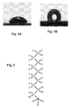
- the glazing angle pictures shown in Figures 1A and 1B were taken by a Kruss G10/DSA10 Drop Shape Analysis System and the contact angle of water droplets onto a virgin silicon wafer not covered by the SAM coating ( Figure 1A ) and of the contact angle of water droplets onto a virgin silicon wafer covered by the SAM coating ( Figure 1 b) .
- the increased contact angle of about 108° clearly shows the hydrophobic nature of the SAM coating.
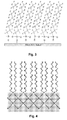
- Figure 2 shows the chemical structure of (Tridecafluoro-1,1,2,2-tetrahydrooctyl)trichlorosilane, C 8 H 4 Cl 3 F 13 Si and its surface organization when self-aligned onto a silicon wafer.
- Figure 3 shows the self-alignment of (Tridecafluoro-1,1,2,2-tetrahydrooctyl)trichlorosilane, C 8 H 4 Cl 3 F 13 Si, onto a silicon wafer resulting from the SAM coating.
- Figure 4 shows the surface condition of a silicon wafer after being exposed to standard atmospheric conditions. Layers of water molecules are adsorbed onto the silicon surface due to hydrogen van der Waals bonds. These layers need to be removed by a mild vacuum heat treatment prior to the application of the SAM coating.
- a typical processing condition is a vacuum dehydratation at about 150°C for about 60 minutes followed by an air exposure of less than about two hours prior to the SAM coating.
- Figure 4 shows the surface condition of a silicon wafer after being vacuum dehydrated at about 150°C for about 60 minutes followed by an air exposure of less than about two hours prior to the SAM coating.
- a series of vacuum pump-downs and dry nitrogen back-fills allow the elimination of the residual oxygen and water vapour present in the atmospheric ambient around the wafers during the loading process.
- a bleeding valve is opened as to allow vapours of (Tridecafluoro-1,1,2,2-tetrahydrooctyl)trichlorosilane, C 8 H 4 Cl 3 F 13 Si, to enter the vacuum chamber at a temperature of about 40°C.
- Pump-down is again performed as to eliminate HCl by-products resulting from the 'SAM treatment'.
- the bleeding valve is again opened as to perform another cycle, and so on. The number of cycles is load dependant and requires to be increased depending upon the surface area of silicon to be treated.
- a filan pump-down followed by a nitrogen purge is used to un-load the 'SAM treated' silicon wafers.
- Figure 6 shows the chemical reactions involved in the self-alignment of (Tridecafluoro-1,1,2,2-tetrahydrooctyl)trichlorosilane, C 8 H 4 Cl 3 F 13 Si, onto dehydrated and air exposed silicon wafers.
- Hydrogen chloride is produced from the chemical reaction of the chlorine atoms residing at the tip of the C 8 H 4 Cl 3 F 13 Si molecules and the hydrogen atoms present at the surface of the dehydrated and air exposed silicon wafers.
- the resulting surface is the one shown Figure 3 .
- a SAM coating 12 is first deposited onto the carrier wafer 10 as shown in Figures 8A and 8B .
- a 20um thick layer 14 of photopolymer is applied by spinning directly onto the SAM coating ( Figure 8C ).
- the thickness of this first layer is adjusted in such a way that it will be strong enough to be used as cover of the microchannel.
- the dried photopolymer is subjected to a pre-exposure bake not exceeding 95°C to drive-off more of its residual solvents in preparation for the exposure to ultra-violet light through a suitably designed mask.
- Figure 8D shows that this 20um thick layer 14 of photopolymer is exposed to ultraviolet light through the openings 16 of the mask 18 defining the shape of the cover of the microchannel.
- the photopolymer Being of negative tone, the photopolymer will reticulate in the regions exposed to the ultraviolet light and will locally become resistant to the chemical attack of the developer to be used later in the process.
- this first layer of a thick negative tone photopolymer is subjected to a post-exposure bake again not exceeding 95°C to drive-off more of the residual solvents and the chemical by-products formed by the ultra-violet light exposure.
- Figure 8E shows that this 20um thick layer of photopolymer is developed, thus defining the cover of the microchannel.
- the regions of the photopolymer that have being exposed to the ultraviolet light passing through the openings of the mask remain intact because resistant to the chemical attack of the developer.
- the resulting photopolymer patterns are subjected to a post-develop bake again not exceeding 95°C to drive-off more of the residual solvents and the chemical by-products formed by the ultra-violet light exposure and by the developer.
- the developed and baked photopolymer patterns of the carrier wafer are ready to be flipped over and aligned to the device wafer.
- Figure 9A shows the silicon wafer 20 used as device wafer substrate.
- a 10um thick layer 22 of photopolymer is applied by spinning. This layer 22 is to become the bottom of the microchannel. Following proper dispensing, spinning and solidification by partial solvents evaporation, the dried photopolymer is subjected to a high temperature bake to drive-off its residual solvents and to allow the photopolymer to be stabilized i.e. to become chemically stable when an upper layer of photopolymer will be spun-on and exposed in a further step.
- a second layer 24 of a 10um thick negative tone photopolymer is then applied by spinning onto the exposed first layer of a thick negative tone photopolymer as shown in Figure 9C .
- This second layer 24 is to become the sidewall of the microchannel.
- the thickness of this second layer is adjusted in such a way that it will form tall enough microchannels confined between the already stabilized bottom layer of the device wafer and the top layer yet to be transferred from the carrier wafer.
- the dried photopolymer is subjected to a pre-exposure bake not exceeding 95°C to drive-off more of its residual solvents in preparation for the exposure to ultra-violet light through a suitably designed mask;
- This second layer 24 of 10um thick negative tone photopolymer is exposed to ultraviolet light through the openings of the mask as shown in Figure 9D .
- the photopolymer Being of negative tone, the photopolymer will reticulate in the regions exposed to the ultraviolet light and will locally become resistant to the chemical attack of the developer to be used later in the process.
- this second layer of a thick negative tone photopolymer is subjected to a post-exposure bake again not exceeding 95°C to drive-off more solvents and chemical by-products formed by the ultra-violet light exposure.
- Figure 9E shows that this second layer 24 of a suitably exposed 10um thick negative tone photopolymer is developed into a proper developer, thus defining the shape of the microchannels.
- the regions of the photopolymer that have being exposed to the ultraviolet light passing through the openings of the mask remain intact because resistant to the chemical attack of the developer.
- the resulting photopolymer patterns are subjected to a post-develop bake again not exceeding 95°C to drive-off more of the residual solvents and the chemical by-products formed by the ultra-violet light exposure and by the develop.
- the developed and baked photopolymer patterns of the Device Wafer are ready to be aligned and to receive the transferred top photopolymer layer of the carrier wafer
- Figure 10A shows that the carrier wafer supporting the developed and baked photopolymer patterns defining the cover of the microchannel is flipped-over and properly aligned to the Device Wafer integrating the sidewall and bottom of the microchannel.
- the precise alignment is such that the aligned wafers, not yet in physical contact, are kept in position using a special fixture in preparation for loading of the pair of wafers into a wafer bonding equipment.
- Figure 10B shows the pair of properly aligned wafers ready to be loaded into wafer bonding equipment that allows these to become in physical contact by pressing one against the other without losing alignment accuracy.
- the pair of wafers is then heated, under vacuum, to a temperature of about 120-150°C while maintaining the two wafers under intimate contact, as to provoke the bonding of the photopolymer of the carrier wafer to the exposed photopolymer of the device wafer.
- the pair of wafers is unloaded from the wafer bonding equipment and the two wafers are separated.
- FIG 10C shows that the MEMS device after separation of the two wafers.
- the separation is possible due to the hydrophobic nature of the SAM coating.
- This wafer separation can be performed using an EVG-850DB wafer debonder.
- the device now incorporating the microchannels 26 is heated under vacuum at more than 200°C as to chemically stabilize the photopolymer and as to achieve a solid permanent microchannel.
- Embodiments of the invention thus provide a novel, simple, inexpensive, high precision, gold-free, sodium-free and potassium-free process allowing the formation, at a temperature of less than 250°C, of hundreds if not thousands of microfluidics microchannels on a CMOS wafer integrating hundreds if not thousands of digital and/or analog CMOS control logic and/or high voltage CMOS drivers capable of performing sensing and/or microfluidics actuation functions.
- This new BioMEMS fabrication process uses an hydrophobic self-aligned monolayer, SAM, as temporary adhesion layer between a Carrier Wafer and the hundreds if not thousands of photolithographically defined microfluidics microchannels to be transferred onto the Device Wafer integrating hundreds if not thousands of digital and/or analog CMOS control logic and/or high voltage CMOS drivers capable of performing sensing and/or microfluidics actuation functions.
- SAM hydrophobic self-aligned monolayer
- the silicon wafer used as the carrier wafer is preferably a SEMI standard 150mm diameter silicon wafer but could also be a 100mm diameter, a 200mm diameter or a 300mm diameter silicon wafer.
- the preferred 20um thick layer 14 of a negative tone photopolymer is applied by spinning onto the SAM coating.
- a preferred photopolymer is SU-8, a negative tone epoxy-like near-UV photoresist developed by IBM and disclosed in USA Patent 4,882,245 entitled: 'Photoresist Composition and Printed Circuit Boards and Packages Made Therewith'.
- This high performance photopolymer is available from three companies: MicroChem Corporation, a company previously named Microlithography Chemical Corporation, of Newton, MA, USA.
- the photopolymer is sold under the name NANO SU-8 at different viscosities: SU-8 2005; SU-8 2010; SU-8 2025; SU-8 2050; SU-8 2100; Gerstel Ltd, a company previously named SOTEC Microsystems, of Pully, Switzerland.
- the photopolymer is sold under the name GM or GLM at different viscosities: GM1040; GM1060; GM1070, GLM2060, GLM3060; and Kayaku Microchem Corporation (KMCC), of Chiyoda-Ku, Tokyo, Japan.
- the photopolymer is sold under the name XP KMPR-1000 SU8 at different viscosities: XP KMPR-1005; XP KMPR-1010; XP KMPR-1025; XP KMPR-1 050; XP KMPR-1100.
- This high performance photopolymer may be spin coated using one of the two coat stations of an EV Group Hercules processor.
- About 3ml of Microchem SU-8 2025 photopolymer solution is dispensed above the 150mm wafer before spinning at about 1600 RPM as to dry the spin-on photopolymer by partial solvents evaporation and as to achieve a film thickness of preferably 20um to be strong enough to become the protection capsule.
- the dried photopolymer is subjected to a pre-exposure bake not exceeding 95°C and for about 8 to 10 minutes as to drive-off more of its residual solvents.
- This MicroChem SU-8 2025 negative tone photopolymer can alternately be replaced by the Gerstel GM 1060 or GLM2060 negative tone photopolymer or by the Kayaku Microchem XP KMPR 1025 negative tone photopolymer to achieve the same preferred thickness of 20um.
- the viscosity of the photopolymer solution could be lower than the one of the Microchem SU-8 2025 photopolymer solution as to reduce the thickness of this first layer of negative tone photopolymer from 40um down to about 5um.
- the Microchem SU-8 2005 or SU-8 2010 negative tone photopolymer solution could be used, the Gerstel GM 1040 negative tone photopolymer solution could be used, or the Kayaku Microchem XP KMPR 1005 or XP KMPR-1010 negative tone photopolymer solution could be used.
- the viscosity of the photopolymer solution could be higher than the one of the Microchem SU-8 2025 photopolymer solution as to increase the thickness of this first layer of negative tone photopolymer from 20um up to about 500um.
- the Microchem SU-8 2050 or SU-8 2100 negative tone photopolymer solution could be used, the Gerstel GM 1070 negative tone photopolymer solution could be used, or the Kayaku Microchem XP KMPR 1050 or XP KMPR-1100 negative tone photopolymer solution could be used.
- To thicker negative tone photopolymer layers should be associated a longer than 90 seconds pre-exposure bake but still not exceeding 95°C and for about as to drive-off the residual solvents.
- Figure 8D shows that this preferably 20um thick layer of negative tone photopolymer is exposed using the highly collimated broadband UV source (g-line, h-line and l-line) of the EV Group Hercules processor through the openings of the mask defining the shape of the protection capsule.
- the photopolymer Being of negative tone, the photopolymer will reticulate in the regions exposed to the ultraviolet light and will locally become resistant to the chemical attack of the developer to be used later in the process.
- this first layer of a thick negative tone photopolymer is subjected to a 5 minutes duration post-exposure bake again not exceeding 95°C as to drive-off more of the residual solvents and the chemical by-products formed by the ultra-violet light exposure. At this point, the exposed photopolymer is not yet developed.
- Figure 8E shows that this preferably 20um thick layer of MicroChem SU-8 2025 negative tone photopolymer is developed using one of the two develop stations of the EV Group Hercules processor to define an array of covers to be transferred onto the array of microchannels of another substrate.
- the regions of the photopolymer that have being exposed to the ultraviolet light passing through the openings of the mask remain intact because resistant to the chemical attack of the developer.
- This layer of negative tone photopolymers is capable of achieving complex structures and mechanical features having a height: width aspect ratio as high as 10:1.
- Figure 9A shows the silicon wafer used as Device Wafer substrate.
- This silicon wafer is preferably a SEMI standard 150mm diameter silicon wafer but could also be a 100mm diameter, a 200mm diameter or a 300mm diameter silicon wafer;
- Figure 9B shows that a first layer of a preferably 10um thick layer negative tone photopolymer is applied by spinning. This first layer is to become an array of bottoms of the array of microchannels.
- This negative tone photopolymer is spin coated using one of the two coat stations of the EV Group Hercules processor shown in Figure 31. Again, about 3ml of Microchem SU-8 2005 is dispensed above the 150mm wafer before spinning at about 1600 RPM as to dry the spin-on photopolymer by partial solvents evaporation and as to achieve a film thickness of preferably 10um. The dried photopolymer is subjected to a pre-exposure bake not exceeding 95°C and for about 5 minutes as to drive-off more of its residual solvents.
- This MicroChem SU-8 2005 negative tone photopolymer can alternately be replaced by the MicroChem SU-8 2010, the Gerstel GM 1040 or the Kayaku Microchem XP KMPR 1005 or XP KMPR 1010 negative tone photopolymer to achieve the same preferred thickness of 10um.
- the viscosity of the photopolymer solution could be higher than the one of the MicroChem SU-8 2005 photopolymer solution as to increase its thickness above 10um.
- the Microchem SU-8 2025 or SU-8 2050 or SU-8 2100, the Gerstel GM 1060, GM 1070 or GM 2060 or the Kayaku Microchem XP KMPR 1025, XP KMPR 1050 or XP KMPR-1100 negative tone photopolymer solution could be used.
- to thicker negative tone photopolymer layers should be associated a longer than 90 seconds pre-exposure bake at about 95°C as to drive-off more of its residual solvents.
- a vacuum bake at a temperature of about 180°C is performed for about 2 hours to stabilize this first 10um thick layer and prevent its photochemical activity when exposed to ultra-violet light.
- Figure 9C shows that a second layer of a preferably 10um thick negative tone photopolymer is applied by spinning onto the thermally stabilized 10um thick negative tone photopolymer.
- this high performance photopolymer is spin coated using one of the two coat stations of the EV Group Hercules processor shown in Figure 31.
- about 3ml of Microchem SU-8 2005 is dispensed above the 150mm wafer before spinning at about 1600 RPM as to dry the spin-on photopolymer by partial solvents evaporation and as to achieve a 10um thick film.
- the dried photopolymer is subjected to a pre-exposure bake not exceeding 95°C and for about 5 minutes as to drive-off more of its residual solvents.
- This MicroChem SU-8 2005 negative tone photopolymer can alternately be replaced by the MicroChem SU-8 2010, the Gerstel GM 1040 or the Kayaku Microchem XP KMPR 1005 or XP KMPR 1010 negative tone photopolymer to achieve the same preferred thickness of 10um.
- the viscosity of the photopolymer solution could be higher than the one of the MicroChem SU-8 2005 photopolymer solution as to increase its thickness above 10um.
- the Microchem SU-8 2025 or SU-8 2050 or SU-8 2100, the Gerstel GM 1060, GM 1070 or GM 2060 or the Kayaku Microchem XP KMPR 1025, XP KMPR 1050 or XP KMPR-1100 negative tone photopolymer solution could be used.
- to thicker negative tone photopolymer layers should be associated a longer than 90 seconds pre-exposure bake but still not exceeding 95°C and for about as to drive-off more of its residual solvents in preparation for the exposure to ultra-violet light through a properly designed mask.
- Figure 9D shows that this second layer of a preferably 10um thick MicroChem SU-8 2005 negative tone photopolymer is exposed using the highly collimated broadband UV source (g-line, h-line and I-line) of the EV Group Hercules processor through the openings of the mask defining the array of sidewalls of the array of microchannels. Being of negative tone, the photopolymer will reticulate in the regions exposed to the ultraviolet light and will locally become resistant to the chemical attack of the developer to be used later in the process.
- the highly collimated broadband UV source g-line, h-line and I-line
- this first layer of a thick negative tone photopolymer is subjected to a 3 minutes duration post-exposure bake again not exceeding 95°C as to drive-off more of the residual solvents and the chemical by-products formed by the ultra-violet light exposure.
- Figure 9E shows that this second layer of a preferably 10um thick MicroChem SU-8 2005 negative tone photopolymer is developed using one of the two develop stations of the EV Group Hercules processor to define the defining the array of sidewalls of the array of microchannels.
- the regions of the photopolymer that have being exposed to the ultraviolet light passing through the openings of one or both of the masks remain intact because resistant to the chemical attack of the developer.
- These two layers of negative tone photopolymers are capable of achieving complex structures and mechanical features having a height: width aspect ratio as high as 10:1.
- the resulting photopolymer patterns are subjected to a post-develop bake at about 95°C as to drive-off more of the residual solvents and the chemical by-products formed by the ultra-violet light exposure and by the develop.
- a vacuum bake at a temperature of about 180°C is performed for about 2 hours to stabilize this exposed second 10um thick layer.
- the developed and baked photopolymer patterns of the Device Wafer are ready to be aligned and to receive the transferred top photopolymer layer of the Carrier Wafer.
- Figure 10A shows that the Carrier Wafer supporting the developed and baked photopolymer patterns defining the array of covers of the array of microchannels is flipped-over and properly aligned to the Device Wafer integrating the array of sidewalls and the array of bottoms of the array of microchannels using the SmartView aligner of an EV Group Gemini processor.
- the alignment is precise within about 1 um.
- the aligned wafers, not yet in physical contact, are kept in position using a special fixture in preparation for loading of the pair of wafers into one of the four Universal bond chamber of the EV Group Gemini processor.
- Figure 10B shows that the pair of properly aligned wafers are loaded into one of the four Universal bond chamber of the EV Group Gemini processor.
- This Universal bond chamber allows the Carrier Wafer and the Device Wafer to become in physical contact by slowly pressing one against the other (without losing alignment accuracy) with a uniform force of 5kN to 20kN while heating the two wafers at a temperature of about 120-150°C for about 20 minutes as to provoke the permanent bonding of the photopolymer of the CARRIER wafer to the exposed top bond material of the Device Wafer.
- the precise alignment of about 1 um achieved with the SmartView is such that the thousands of protection capsules of the CARRIER wafer do not make a direct contact to the thousands of free-to-move mechanical devices of the Device Wafer during this bonding process.
- the bonded pair of wafers is unloaded from the Universal bond chamber, cooled-down to room temperature using a cool station and returned in a properly designed receiving cassette.
- FIG 10C shows that the two wafers are separated from each other. This is possible due to the hydrophobic nature of the SAM coating. This wafer separation can be performed using an EVG-850DB wafer debonder.
- Figure 10D shows that the Device Wafer now incorporating the microchannel is heated under vacuum at more than 200°C as to chemically stabilize the photopolymer and as to achieve a solid permanent microchannel.
Landscapes
- Engineering & Computer Science (AREA)
- Chemical & Material Sciences (AREA)
- Physics & Mathematics (AREA)
- General Physics & Mathematics (AREA)
- Nanotechnology (AREA)
- Manufacturing & Machinery (AREA)
- Microelectronics & Electronic Packaging (AREA)
- Composite Materials (AREA)
- Condensed Matter Physics & Semiconductors (AREA)
- Materials Engineering (AREA)
- Crystallography & Structural Chemistry (AREA)
- Analytical Chemistry (AREA)
- Micromachines (AREA)
Applications Claiming Priority (1)
| Application Number | Priority Date | Filing Date | Title |
|---|---|---|---|
| US14254309P | 2009-01-05 | 2009-01-05 |
Publications (3)
| Publication Number | Publication Date |
|---|---|
| EP2204348A2 true EP2204348A2 (fr) | 2010-07-07 |
| EP2204348A3 EP2204348A3 (fr) | 2011-05-18 |
| EP2204348B1 EP2204348B1 (fr) | 2013-05-29 |
Family
ID=41667343
Family Applications (1)
| Application Number | Title | Priority Date | Filing Date |
|---|---|---|---|
| EP10150112.0A Active EP2204348B1 (fr) | 2009-01-05 | 2010-01-05 | Procédé de fabrication de dispositifs BIO-MEMS |
Country Status (2)
| Country | Link |
|---|---|
| US (1) | US7927904B2 (fr) |
| EP (1) | EP2204348B1 (fr) |
Families Citing this family (47)
| Publication number | Priority date | Publication date | Assignee | Title |
|---|---|---|---|---|
| US8421844B2 (en) | 2010-08-13 | 2013-04-16 | Alcatel Lucent | Apparatus for correcting gaze, a method of videoconferencing and a system therefor |
| US20120094418A1 (en) * | 2010-10-18 | 2012-04-19 | Triquint Semiconductor, Inc. | Wafer Level Package and Manufacturing Method Using Photodefinable Polymer for Enclosing Acoustic Devices |
| US20130320481A1 (en) * | 2012-06-01 | 2013-12-05 | Bridge Semiconductor Corporation | High Density Pyroelectric Thin Film Infrared Sensor Array and Method of Manufacture Thereof |
| US9812350B2 (en) | 2013-03-06 | 2017-11-07 | Qorvo Us, Inc. | Method of manufacture for a silicon-on-plastic semiconductor device with interfacial adhesion layer |
| US9583414B2 (en) | 2013-10-31 | 2017-02-28 | Qorvo Us, Inc. | Silicon-on-plastic semiconductor device and method of making the same |
| TWI533929B (zh) * | 2013-12-13 | 2016-05-21 | 財團法人國家實驗研究院 | 微流道檢測系統及其製造方法 |
| EP2996143B1 (fr) | 2014-09-12 | 2018-12-26 | Qorvo US, Inc. | Module de circuit imprimé comportant un dispositif à semi-conducteur avec un substrat polymère et procédés de sa fabrication |
| US10085352B2 (en) | 2014-10-01 | 2018-09-25 | Qorvo Us, Inc. | Method for manufacturing an integrated circuit package |
| US9530709B2 (en) | 2014-11-03 | 2016-12-27 | Qorvo Us, Inc. | Methods of manufacturing a printed circuit module having a semiconductor device with a protective layer in place of a low-resistivity handle layer |
| US9960145B2 (en) | 2015-03-25 | 2018-05-01 | Qorvo Us, Inc. | Flip chip module with enhanced properties |
| US9613831B2 (en) | 2015-03-25 | 2017-04-04 | Qorvo Us, Inc. | Encapsulated dies with enhanced thermal performance |
| US20160343604A1 (en) | 2015-05-22 | 2016-11-24 | Rf Micro Devices, Inc. | Substrate structure with embedded layer for post-processing silicon handle elimination |
| US10276495B2 (en) | 2015-09-11 | 2019-04-30 | Qorvo Us, Inc. | Backside semiconductor die trimming |
| DE102015224545A1 (de) * | 2015-12-08 | 2017-06-08 | Robert Bosch Gmbh | Verfahren zum Herstellen eines mikromechanisches Bauelements |
| US10020405B2 (en) | 2016-01-19 | 2018-07-10 | Qorvo Us, Inc. | Microelectronics package with integrated sensors |
| US10062583B2 (en) | 2016-05-09 | 2018-08-28 | Qorvo Us, Inc. | Microelectronics package with inductive element and magnetically enhanced mold compound component |
| US10773952B2 (en) | 2016-05-20 | 2020-09-15 | Qorvo Us, Inc. | Wafer-level package with enhanced performance |
| US10784149B2 (en) | 2016-05-20 | 2020-09-22 | Qorvo Us, Inc. | Air-cavity module with enhanced device isolation |
| US10103080B2 (en) | 2016-06-10 | 2018-10-16 | Qorvo Us, Inc. | Thermally enhanced semiconductor package with thermal additive and process for making the same |
| US10079196B2 (en) | 2016-07-18 | 2018-09-18 | Qorvo Us, Inc. | Thermally enhanced semiconductor package having field effect transistors with back-gate feature |
| CN109844938B (zh) | 2016-08-12 | 2023-07-18 | Qorvo美国公司 | 具有增强性能的晶片级封装 |
| SG11201901193UA (en) | 2016-08-12 | 2019-03-28 | Qorvo Us Inc | Wafer-level package with enhanced performance |
| US10486965B2 (en) | 2016-08-12 | 2019-11-26 | Qorvo Us, Inc. | Wafer-level package with enhanced performance |
| US10109502B2 (en) | 2016-09-12 | 2018-10-23 | Qorvo Us, Inc. | Semiconductor package with reduced parasitic coupling effects and process for making the same |
| US10090339B2 (en) | 2016-10-21 | 2018-10-02 | Qorvo Us, Inc. | Radio frequency (RF) switch |
| US10749518B2 (en) | 2016-11-18 | 2020-08-18 | Qorvo Us, Inc. | Stacked field-effect transistor switch |
| US10068831B2 (en) | 2016-12-09 | 2018-09-04 | Qorvo Us, Inc. | Thermally enhanced semiconductor package and process for making the same |
| US10490471B2 (en) | 2017-07-06 | 2019-11-26 | Qorvo Us, Inc. | Wafer-level packaging for enhanced performance |
| US10784233B2 (en) | 2017-09-05 | 2020-09-22 | Qorvo Us, Inc. | Microelectronics package with self-aligned stacked-die assembly |
| US10366972B2 (en) | 2017-09-05 | 2019-07-30 | Qorvo Us, Inc. | Microelectronics package with self-aligned stacked-die assembly |
| US11152363B2 (en) | 2018-03-28 | 2021-10-19 | Qorvo Us, Inc. | Bulk CMOS devices with enhanced performance and methods of forming the same utilizing bulk CMOS process |
| US12062700B2 (en) | 2018-04-04 | 2024-08-13 | Qorvo Us, Inc. | Gallium-nitride-based module with enhanced electrical performance and process for making the same |
| US12046505B2 (en) | 2018-04-20 | 2024-07-23 | Qorvo Us, Inc. | RF devices with enhanced performance and methods of forming the same utilizing localized SOI formation |
| US10804246B2 (en) | 2018-06-11 | 2020-10-13 | Qorvo Us, Inc. | Microelectronics package with vertically stacked dies |
| US20200006193A1 (en) | 2018-07-02 | 2020-01-02 | Qorvo Us, Inc. | Rf devices with enhanced performance and methods of forming the same |
| US11069590B2 (en) | 2018-10-10 | 2021-07-20 | Qorvo Us, Inc. | Wafer-level fan-out package with enhanced performance |
| US10964554B2 (en) | 2018-10-10 | 2021-03-30 | Qorvo Us, Inc. | Wafer-level fan-out package with enhanced performance |
| US11646242B2 (en) | 2018-11-29 | 2023-05-09 | Qorvo Us, Inc. | Thermally enhanced semiconductor package with at least one heat extractor and process for making the same |
| US12046570B2 (en) | 2019-01-23 | 2024-07-23 | Qorvo Us, Inc. | RF devices with enhanced performance and methods of forming the same |
| US11387157B2 (en) | 2019-01-23 | 2022-07-12 | Qorvo Us, Inc. | RF devices with enhanced performance and methods of forming the same |
| US12057374B2 (en) | 2019-01-23 | 2024-08-06 | Qorvo Us, Inc. | RF devices with enhanced performance and methods of forming the same |
| US12046483B2 (en) | 2019-01-23 | 2024-07-23 | Qorvo Us, Inc. | RF devices with enhanced performance and methods of forming the same |
| KR20210129656A (ko) | 2019-01-23 | 2021-10-28 | 코르보 유에스, 인크. | Rf 반도체 디바이스 및 이를 형성하는 방법 |
| US12074086B2 (en) | 2019-11-01 | 2024-08-27 | Qorvo Us, Inc. | RF devices with nanotube particles for enhanced performance and methods of forming the same |
| US11646289B2 (en) | 2019-12-02 | 2023-05-09 | Qorvo Us, Inc. | RF devices with enhanced performance and methods of forming the same |
| US11923238B2 (en) | 2019-12-12 | 2024-03-05 | Qorvo Us, Inc. | Method of forming RF devices with enhanced performance including attaching a wafer to a support carrier by a bonding technique without any polymer adhesive |
| US12062571B2 (en) | 2021-03-05 | 2024-08-13 | Qorvo Us, Inc. | Selective etching process for SiGe and doped epitaxial silicon |
Citations (81)
| Publication number | Priority date | Publication date | Assignee | Title |
|---|---|---|---|---|
| US4882245A (en) | 1985-10-28 | 1989-11-21 | International Business Machines Corporation | Photoresist composition and printed circuit boards and packages made therewith |
| US5376252A (en) | 1990-05-10 | 1994-12-27 | Pharmacia Biosensor Ab | Microfluidic structure and process for its manufacture |
| US5591139A (en) | 1994-06-06 | 1997-01-07 | The Regents Of The University Of California | IC-processed microneedles |
| US5699157A (en) | 1996-07-16 | 1997-12-16 | Caliper Technologies Corp. | Fourier detection of species migrating in a microchannel |
| US5705018A (en) | 1995-12-13 | 1998-01-06 | Hartley; Frank T. | Micromachined peristaltic pump |
| US5716852A (en) | 1996-03-29 | 1998-02-10 | University Of Washington | Microfabricated diffusion-based chemical sensor |
| US5755942A (en) | 1994-11-10 | 1998-05-26 | David Sarnoff Research Center, Inc. | Partitioned microelectronic device array |
| US5779868A (en) | 1996-06-28 | 1998-07-14 | Caliper Technologies Corporation | Electropipettor and compensation means for electrophoretic bias |
| US5800690A (en) | 1996-07-03 | 1998-09-01 | Caliper Technologies Corporation | Variable control of electroosmotic and/or electrophoretic forces within a fluid-containing structure via electrical forces |
| US5842787A (en) | 1997-10-09 | 1998-12-01 | Caliper Technologies Corporation | Microfluidic systems incorporating varied channel dimensions |
| US5849208A (en) | 1995-09-07 | 1998-12-15 | Microfab Technoologies, Inc. | Making apparatus for conducting biochemical analyses |
| US5856174A (en) | 1995-06-29 | 1999-01-05 | Affymetrix, Inc. | Integrated nucleic acid diagnostic device |
| US5863502A (en) | 1996-01-24 | 1999-01-26 | Sarnoff Corporation | Parallel reaction cassette and associated devices |
| US5869004A (en) | 1997-06-09 | 1999-02-09 | Caliper Technologies Corp. | Methods and apparatus for in situ concentration and/or dilution of materials in microfluidic systems |
| US5876675A (en) | 1997-08-05 | 1999-03-02 | Caliper Technologies Corp. | Microfluidic devices and systems |
| US5882465A (en) | 1997-06-18 | 1999-03-16 | Caliper Technologies Corp. | Method of manufacturing microfluidic devices |
| US5885470A (en) | 1997-04-14 | 1999-03-23 | Caliper Technologies Corporation | Controlled fluid transport in microfabricated polymeric substrates |
| US5922604A (en) | 1997-06-05 | 1999-07-13 | Gene Tec Corporation | Thin reaction chambers for containing and handling liquid microvolumes |
| US5922210A (en) | 1995-06-16 | 1999-07-13 | University Of Washington | Tangential flow planar microfabricated fluid filter and method of using thereof |
| US5932100A (en) | 1995-06-16 | 1999-08-03 | University Of Washington | Microfabricated differential extraction device and method |
| US5932315A (en) | 1997-04-30 | 1999-08-03 | Hewlett-Packard Company | Microfluidic structure assembly with mating microfeatures |
| US5942443A (en) | 1996-06-28 | 1999-08-24 | Caliper Technologies Corporation | High throughput screening assay systems in microscale fluidic devices |
| US5948684A (en) | 1997-03-31 | 1999-09-07 | University Of Washington | Simultaneous analyte determination and reference balancing in reference T-sensor devices |
| US5948227A (en) | 1997-12-17 | 1999-09-07 | Caliper Technologies Corp. | Methods and systems for performing electrophoretic molecular separations |
| US5955028A (en) | 1996-08-02 | 1999-09-21 | Caliper Technologies Corp. | Analytical system and method |
| US5958694A (en) | 1997-10-16 | 1999-09-28 | Caliper Technologies Corp. | Apparatus and methods for sequencing nucleic acids in microfluidic systems |
| US5958203A (en) | 1996-06-28 | 1999-09-28 | Caliper Technologies Corportion | Electropipettor and compensation means for electrophoretic bias |
| US5964995A (en) | 1997-04-04 | 1999-10-12 | Caliper Technologies Corp. | Methods and systems for enhanced fluid transport |
| US5965410A (en) | 1997-09-02 | 1999-10-12 | Caliper Technologies Corp. | Electrical current for controlling fluid parameters in microchannels |
| US5980719A (en) | 1997-05-13 | 1999-11-09 | Sarnoff Corporation | Electrohydrodynamic receptor |
| US5989402A (en) | 1997-08-29 | 1999-11-23 | Caliper Technologies Corp. | Controller/detector interfaces for microfluidic systems |
| US5992820A (en) | 1997-11-19 | 1999-11-30 | Sarnoff Corporation | Flow control in microfluidics devices by controlled bubble formation |
| US6001231A (en) | 1997-07-15 | 1999-12-14 | Caliper Technologies Corp. | Methods and systems for monitoring and controlling fluid flow rates in microfluidic systems |
| US6007775A (en) | 1997-09-26 | 1999-12-28 | University Of Washington | Multiple analyte diffusion based chemical sensor |
| US6011252A (en) | 1997-06-27 | 2000-01-04 | Caliper Technologies Corp. | Method and apparatus for detecting low light levels |
| US6012902A (en) | 1997-09-25 | 2000-01-11 | Caliper Technologies Corp. | Micropump |
| US6048734A (en) | 1995-09-15 | 2000-04-11 | The Regents Of The University Of Michigan | Thermal microvalves in a fluid flow method |
| US6054277A (en) | 1996-05-08 | 2000-04-25 | Regents Of The University Of Minnesota | Integrated microchip genetic testing system |
| US6056269A (en) | 1999-01-15 | 2000-05-02 | Hewlett-Packard Company | Microminiature valve having silicon diaphragm |
| US6057149A (en) | 1995-09-15 | 2000-05-02 | The University Of Michigan | Microscale devices and reactions in microscale devices |
| US6062261A (en) | 1998-12-16 | 2000-05-16 | Lockheed Martin Energy Research Corporation | MicrofluIdic circuit designs for performing electrokinetic manipulations that reduce the number of voltage sources and fluid reservoirs |
| US6063589A (en) | 1997-05-23 | 2000-05-16 | Gamera Bioscience Corporation | Devices and methods for using centripetal acceleration to drive fluid movement on a microfluidics system |
| US6068752A (en) | 1997-04-25 | 2000-05-30 | Caliper Technologies Corp. | Microfluidic devices incorporating improved channel geometries |
| US6073482A (en) | 1997-07-21 | 2000-06-13 | Ysi Incorporated | Fluid flow module |
| US6074725A (en) | 1997-12-10 | 2000-06-13 | Caliper Technologies Corp. | Fabrication of microfluidic circuits by printing techniques |
| US6074827A (en) | 1996-07-30 | 2000-06-13 | Aclara Biosciences, Inc. | Microfluidic method for nucleic acid purification and processing |
| US6078340A (en) | 1997-09-26 | 2000-06-20 | Eastman Kodak Company | Using silver salts and reducing reagents in microfluidic printing |
| US6082140A (en) | 1999-06-16 | 2000-07-04 | The Regents Of The University Of California | Fusion bonding and alignment fixture |
| US6086740A (en) | 1998-10-29 | 2000-07-11 | Caliper Technologies Corp. | Multiplexed microfluidic devices and systems |
| US6086825A (en) | 1997-06-06 | 2000-07-11 | Caliper Technologies Corporation | Microfabricated structures for facilitating fluid introduction into microfluidic devices |
| US6091502A (en) | 1998-12-23 | 2000-07-18 | Micronics, Inc. | Device and method for performing spectral measurements in flow cells with spatial resolution |
| US6096656A (en) | 1999-06-24 | 2000-08-01 | Sandia Corporation | Formation of microchannels from low-temperature plasma-deposited silicon oxynitride |
| US6100541A (en) | 1998-02-24 | 2000-08-08 | Caliper Technologies Corporation | Microfluidic devices and systems incorporating integrated optical elements |
| US6103199A (en) | 1998-09-15 | 2000-08-15 | Aclara Biosciences, Inc. | Capillary electroflow apparatus and method |
| US6106685A (en) | 1997-05-13 | 2000-08-22 | Sarnoff Corporation | Electrode combinations for pumping fluids |
| US6117643A (en) | 1997-11-25 | 2000-09-12 | Ut Battelle, Llc | Bioluminescent bioreporter integrated circuit |
| US6118126A (en) | 1997-10-31 | 2000-09-12 | Sarnoff Corporation | Method for enhancing fluorescence |
| US6120666A (en) | 1996-09-26 | 2000-09-19 | Ut-Battelle, Llc | Microfabricated device and method for multiplexed electrokinetic focusing of fluid streams and a transport cytometry method using same |
| US6123798A (en) | 1998-05-06 | 2000-09-26 | Caliper Technologies Corp. | Methods of fabricating polymeric structures incorporating microscale fluidic elements |
| US6126140A (en) | 1997-12-29 | 2000-10-03 | Honeywell International Inc. | Monolithic bi-directional microvalve with enclosed drive electric field |
| US6126765A (en) | 1993-06-15 | 2000-10-03 | Pharmacia Biotech Ab | Method of producing microchannel/microcavity structures |
| US6129854A (en) | 1996-05-16 | 2000-10-10 | Ut-Battelle, Llc | Low temperature material bonding technique |
| US6130098A (en) | 1995-09-15 | 2000-10-10 | The Regents Of The University Of Michigan | Moving microdroplets |
| US6132685A (en) | 1998-08-10 | 2000-10-17 | Caliper Technologies Corporation | High throughput microfluidic systems and methods |
| US6131410A (en) | 1998-03-16 | 2000-10-17 | The Regents Of The University Of California | Vacuum fusion bonding of glass plates |
| US6136272A (en) | 1997-09-26 | 2000-10-24 | University Of Washington | Device for rapidly joining and splitting fluid layers |
| US6136212A (en) | 1996-08-12 | 2000-10-24 | The Regents Of The University Of Michigan | Polymer-based micromachining for microfluidic devices |
| US6137501A (en) | 1997-09-19 | 2000-10-24 | Eastman Kodak Company | Addressing circuitry for microfluidic printing apparatus |
| US6143152A (en) | 1997-11-07 | 2000-11-07 | The Regents Of The University Of California | Microfabricated capillary array electrophoresis device and method |
| US6143248A (en) | 1996-08-12 | 2000-11-07 | Gamera Bioscience Corp. | Capillary microvalve |
| US6146103A (en) | 1998-10-09 | 2000-11-14 | The Regents Of The University Of California | Micromachined magnetohydrodynamic actuators and sensors |
| US6148508A (en) | 1999-03-12 | 2000-11-21 | Caliper Technologies Corp. | Method of making a capillary for electrokinetic transport of materials |
| US6150119A (en) | 1999-01-19 | 2000-11-21 | Caliper Technologies Corp. | Optimized high-throughput analytical system |
| US6149787A (en) | 1998-10-14 | 2000-11-21 | Caliper Technologies Corp. | External material accession systems and methods |
| US6154226A (en) | 1997-05-13 | 2000-11-28 | Sarnoff Corporation | Parallel print array |
| US6159739A (en) | 1997-03-26 | 2000-12-12 | University Of Washington | Device and method for 3-dimensional alignment of particles in microfabricated flow channels |
| US6167910B1 (en) | 1998-01-20 | 2001-01-02 | Caliper Technologies Corp. | Multi-layer microfluidic devices |
| US6170981B1 (en) | 1998-05-07 | 2001-01-09 | Purdue Research Foundation | In situ micromachined mixer for microfluidic analytical systems |
| US6171850B1 (en) | 1999-03-08 | 2001-01-09 | Caliper Technologies Corp. | Integrated devices and systems for performing temperature controlled reactions and analyses |
| US6174675B1 (en) | 1997-11-25 | 2001-01-16 | Caliper Technologies Corp. | Electrical current for controlling fluid parameters in microchannels |
| US6180536B1 (en) | 1998-06-04 | 2001-01-30 | Cornell Research Foundation, Inc. | Suspended moving channels and channel actuators for microfluidic applications and method for making |
Family Cites Families (8)
| Publication number | Priority date | Publication date | Assignee | Title |
|---|---|---|---|---|
| US6902947B2 (en) * | 2001-05-07 | 2005-06-07 | Applied Materials, Inc. | Integrated method for release and passivation of MEMS structures |
| US7060227B2 (en) * | 2001-08-06 | 2006-06-13 | Sau Lan Tang Staats | Microfluidic devices with raised walls |
| US6805809B2 (en) * | 2002-08-28 | 2004-10-19 | Board Of Trustees Of University Of Illinois | Decal transfer microfabrication |
| US7282254B1 (en) * | 2004-02-23 | 2007-10-16 | The Research Foundation Of State University Of New York | Surface coating for electronic systems |
| US8025831B2 (en) * | 2004-05-24 | 2011-09-27 | Agency For Science, Technology And Research | Imprinting of supported and free-standing 3-D micro- or nano-structures |
| WO2006050496A1 (fr) * | 2004-11-02 | 2006-05-11 | E.I. Dupont De Nemours And Company | Anthracenes substitues et dispositifs electroniques contenant les anthracenes substitues |
| KR20070067442A (ko) * | 2005-12-23 | 2007-06-28 | 삼성전자주식회사 | 기판으로부터 포토레지스트 막을 분리하는 방법 및 상기포토레지스트 막을 이차 기판과 접합하는 방법 |
| US7682860B2 (en) * | 2006-03-21 | 2010-03-23 | Dalsa Semiconductor Inc. | Protection capsule for MEMS devices |
-
2010
- 2010-01-04 US US12/651,561 patent/US7927904B2/en active Active
- 2010-01-05 EP EP10150112.0A patent/EP2204348B1/fr active Active
Patent Citations (107)
| Publication number | Priority date | Publication date | Assignee | Title |
|---|---|---|---|---|
| US4882245A (en) | 1985-10-28 | 1989-11-21 | International Business Machines Corporation | Photoresist composition and printed circuit boards and packages made therewith |
| US5376252A (en) | 1990-05-10 | 1994-12-27 | Pharmacia Biosensor Ab | Microfluidic structure and process for its manufacture |
| US6126765A (en) | 1993-06-15 | 2000-10-03 | Pharmacia Biotech Ab | Method of producing microchannel/microcavity structures |
| US5591139A (en) | 1994-06-06 | 1997-01-07 | The Regents Of The University Of California | IC-processed microneedles |
| US5855801A (en) | 1994-06-06 | 1999-01-05 | Lin; Liwei | IC-processed microneedles |
| US5755942A (en) | 1994-11-10 | 1998-05-26 | David Sarnoff Research Center, Inc. | Partitioned microelectronic device array |
| US5922210A (en) | 1995-06-16 | 1999-07-13 | University Of Washington | Tangential flow planar microfabricated fluid filter and method of using thereof |
| US5932100A (en) | 1995-06-16 | 1999-08-03 | University Of Washington | Microfabricated differential extraction device and method |
| US5856174A (en) | 1995-06-29 | 1999-01-05 | Affymetrix, Inc. | Integrated nucleic acid diagnostic device |
| US6043080A (en) | 1995-06-29 | 2000-03-28 | Affymetrix, Inc. | Integrated nucleic acid diagnostic device |
| US5849208A (en) | 1995-09-07 | 1998-12-15 | Microfab Technoologies, Inc. | Making apparatus for conducting biochemical analyses |
| US6130098A (en) | 1995-09-15 | 2000-10-10 | The Regents Of The University Of Michigan | Moving microdroplets |
| US6057149A (en) | 1995-09-15 | 2000-05-02 | The University Of Michigan | Microscale devices and reactions in microscale devices |
| US6048734A (en) | 1995-09-15 | 2000-04-11 | The Regents Of The University Of Michigan | Thermal microvalves in a fluid flow method |
| US5705018A (en) | 1995-12-13 | 1998-01-06 | Hartley; Frank T. | Micromachined peristaltic pump |
| US5863502A (en) | 1996-01-24 | 1999-01-26 | Sarnoff Corporation | Parallel reaction cassette and associated devices |
| US5716852A (en) | 1996-03-29 | 1998-02-10 | University Of Washington | Microfabricated diffusion-based chemical sensor |
| US5972710A (en) | 1996-03-29 | 1999-10-26 | University Of Washington | Microfabricated diffusion-based chemical sensor |
| US6171865B1 (en) | 1996-03-29 | 2001-01-09 | University Of Washington | Simultaneous analyte determination and reference balancing in reference T-sensor devices |
| US6156181A (en) | 1996-04-16 | 2000-12-05 | Caliper Technologies, Corp. | Controlled fluid transport microfabricated polymeric substrates |
| US6054277A (en) | 1996-05-08 | 2000-04-25 | Regents Of The University Of Minnesota | Integrated microchip genetic testing system |
| US6129854A (en) | 1996-05-16 | 2000-10-10 | Ut-Battelle, Llc | Low temperature material bonding technique |
| US5958203A (en) | 1996-06-28 | 1999-09-28 | Caliper Technologies Corportion | Electropipettor and compensation means for electrophoretic bias |
| US5779868A (en) | 1996-06-28 | 1998-07-14 | Caliper Technologies Corporation | Electropipettor and compensation means for electrophoretic bias |
| US5942443A (en) | 1996-06-28 | 1999-08-24 | Caliper Technologies Corporation | High throughput screening assay systems in microscale fluidic devices |
| US5972187A (en) | 1996-06-28 | 1999-10-26 | Caliper Technologies Corporation | Electropipettor and compensation means for electrophoretic bias |
| US6150180A (en) | 1996-06-28 | 2000-11-21 | Caliper Technologies Corp. | High throughput screening assay systems in microscale fluidic devices |
| US6046056A (en) | 1996-06-28 | 2000-04-04 | Caliper Technologies Corporation | High throughput screening assay systems in microscale fluidic devices |
| US5880071A (en) | 1996-06-28 | 1999-03-09 | Caliper Technologies Corporation | Electropipettor and compensation means for electrophoretic bias |
| US6080295A (en) | 1996-06-28 | 2000-06-27 | Caliper Technologies Corporation | Electropipettor and compensation means for electrophoretic bias |
| US6042709A (en) | 1996-06-28 | 2000-03-28 | Caliper Technologies Corp. | Microfluidic sampling system and methods |
| US5965001A (en) | 1996-07-03 | 1999-10-12 | Caliper Technologies Corporation | Variable control of electroosmotic and/or electrophoretic forces within a fluid-containing structure via electrical forces |
| US5800690A (en) | 1996-07-03 | 1998-09-01 | Caliper Technologies Corporation | Variable control of electroosmotic and/or electrophoretic forces within a fluid-containing structure via electrical forces |
| US5852495A (en) | 1996-07-16 | 1998-12-22 | Caliper Technologies Corporation | Fourier detection of species migrating in a microchannel |
| US5699157A (en) | 1996-07-16 | 1997-12-16 | Caliper Technologies Corp. | Fourier detection of species migrating in a microchannel |
| US6074827A (en) | 1996-07-30 | 2000-06-13 | Aclara Biosciences, Inc. | Microfluidic method for nucleic acid purification and processing |
| US5955028A (en) | 1996-08-02 | 1999-09-21 | Caliper Technologies Corp. | Analytical system and method |
| US6071478A (en) | 1996-08-02 | 2000-06-06 | Caliper Technologies Corp. | Analytical system and method |
| US6136212A (en) | 1996-08-12 | 2000-10-24 | The Regents Of The University Of Michigan | Polymer-based micromachining for microfluidic devices |
| US6143248A (en) | 1996-08-12 | 2000-11-07 | Gamera Bioscience Corp. | Capillary microvalve |
| US6120666A (en) | 1996-09-26 | 2000-09-19 | Ut-Battelle, Llc | Microfabricated device and method for multiplexed electrokinetic focusing of fluid streams and a transport cytometry method using same |
| US6159739A (en) | 1997-03-26 | 2000-12-12 | University Of Washington | Device and method for 3-dimensional alignment of particles in microfabricated flow channels |
| US5948684A (en) | 1997-03-31 | 1999-09-07 | University Of Washington | Simultaneous analyte determination and reference balancing in reference T-sensor devices |
| US6129826A (en) | 1997-04-04 | 2000-10-10 | Caliper Technologies Corp. | Methods and systems for enhanced fluid transport |
| US5964995A (en) | 1997-04-04 | 1999-10-12 | Caliper Technologies Corp. | Methods and systems for enhanced fluid transport |
| US5885470A (en) | 1997-04-14 | 1999-03-23 | Caliper Technologies Corporation | Controlled fluid transport in microfabricated polymeric substrates |
| US6068752A (en) | 1997-04-25 | 2000-05-30 | Caliper Technologies Corp. | Microfluidic devices incorporating improved channel geometries |
| US6153073A (en) | 1997-04-25 | 2000-11-28 | Caliper Technologies Corp. | Microfluidic devices incorporating improved channel geometries |
| US5932315A (en) | 1997-04-30 | 1999-08-03 | Hewlett-Packard Company | Microfluidic structure assembly with mating microfeatures |
| US5980719A (en) | 1997-05-13 | 1999-11-09 | Sarnoff Corporation | Electrohydrodynamic receptor |
| US6106685A (en) | 1997-05-13 | 2000-08-22 | Sarnoff Corporation | Electrode combinations for pumping fluids |
| US6154226A (en) | 1997-05-13 | 2000-11-28 | Sarnoff Corporation | Parallel print array |
| US6063589A (en) | 1997-05-23 | 2000-05-16 | Gamera Bioscience Corporation | Devices and methods for using centripetal acceleration to drive fluid movement on a microfluidics system |
| US5922604A (en) | 1997-06-05 | 1999-07-13 | Gene Tec Corporation | Thin reaction chambers for containing and handling liquid microvolumes |
| US6086825A (en) | 1997-06-06 | 2000-07-11 | Caliper Technologies Corporation | Microfabricated structures for facilitating fluid introduction into microfluidic devices |
| US6090251A (en) | 1997-06-06 | 2000-07-18 | Caliper Technologies, Inc. | Microfabricated structures for facilitating fluid introduction into microfluidic devices |
| US6149870A (en) | 1997-06-09 | 2000-11-21 | Caliper Technologies Corp. | Apparatus for in situ concentration and/or dilution of materials in microfluidic systems |
| US6004515A (en) | 1997-06-09 | 1999-12-21 | Calipher Technologies Corp. | Methods and apparatus for in situ concentration and/or dilution of materials in microfluidic systems |
| US5869004A (en) | 1997-06-09 | 1999-02-09 | Caliper Technologies Corp. | Methods and apparatus for in situ concentration and/or dilution of materials in microfluidic systems |
| US5882465A (en) | 1997-06-18 | 1999-03-16 | Caliper Technologies Corp. | Method of manufacturing microfluidic devices |
| US6172353B1 (en) | 1997-06-27 | 2001-01-09 | Caliper Technologies Corp. | System and method for measuring low power signals |
| US6011252A (en) | 1997-06-27 | 2000-01-04 | Caliper Technologies Corp. | Method and apparatus for detecting low light levels |
| US6001231A (en) | 1997-07-15 | 1999-12-14 | Caliper Technologies Corp. | Methods and systems for monitoring and controlling fluid flow rates in microfluidic systems |
| US6073482A (en) | 1997-07-21 | 2000-06-13 | Ysi Incorporated | Fluid flow module |
| US6048498A (en) | 1997-08-05 | 2000-04-11 | Caliper Technologies Corp. | Microfluidic devices and systems |
| US5876675A (en) | 1997-08-05 | 1999-03-02 | Caliper Technologies Corp. | Microfluidic devices and systems |
| US5989402A (en) | 1997-08-29 | 1999-11-23 | Caliper Technologies Corp. | Controller/detector interfaces for microfluidic systems |
| US5965410A (en) | 1997-09-02 | 1999-10-12 | Caliper Technologies Corp. | Electrical current for controlling fluid parameters in microchannels |
| US6137501A (en) | 1997-09-19 | 2000-10-24 | Eastman Kodak Company | Addressing circuitry for microfluidic printing apparatus |
| US6171067B1 (en) | 1997-09-25 | 2001-01-09 | Caliper Technologies Corp. | Micropump |
| US6012902A (en) | 1997-09-25 | 2000-01-11 | Caliper Technologies Corp. | Micropump |
| US6078340A (en) | 1997-09-26 | 2000-06-20 | Eastman Kodak Company | Using silver salts and reducing reagents in microfluidic printing |
| US6007775A (en) | 1997-09-26 | 1999-12-28 | University Of Washington | Multiple analyte diffusion based chemical sensor |
| US6136272A (en) | 1997-09-26 | 2000-10-24 | University Of Washington | Device for rapidly joining and splitting fluid layers |
| US6186660B1 (en) | 1997-10-09 | 2001-02-13 | Caliper Technologies Corp. | Microfluidic systems incorporating varied channel dimensions |
| US5842787A (en) | 1997-10-09 | 1998-12-01 | Caliper Technologies Corporation | Microfluidic systems incorporating varied channel dimensions |
| US5957579A (en) | 1997-10-09 | 1999-09-28 | Caliper Technologies Corp. | Microfluidic systems incorporating varied channel dimensions |
| US5958694A (en) | 1997-10-16 | 1999-09-28 | Caliper Technologies Corp. | Apparatus and methods for sequencing nucleic acids in microfluidic systems |
| US6107044A (en) | 1997-10-16 | 2000-08-22 | Caliper Technologies Corp. | Apparatus and methods for sequencing nucleic acids in microfluidic systems |
| US6118126A (en) | 1997-10-31 | 2000-09-12 | Sarnoff Corporation | Method for enhancing fluorescence |
| US6143152A (en) | 1997-11-07 | 2000-11-07 | The Regents Of The University Of California | Microfabricated capillary array electrophoresis device and method |
| US5992820A (en) | 1997-11-19 | 1999-11-30 | Sarnoff Corporation | Flow control in microfluidics devices by controlled bubble formation |
| US6174675B1 (en) | 1997-11-25 | 2001-01-16 | Caliper Technologies Corp. | Electrical current for controlling fluid parameters in microchannels |
| US6117643A (en) | 1997-11-25 | 2000-09-12 | Ut Battelle, Llc | Bioluminescent bioreporter integrated circuit |
| US6074725A (en) | 1997-12-10 | 2000-06-13 | Caliper Technologies Corp. | Fabrication of microfluidic circuits by printing techniques |
| US5948227A (en) | 1997-12-17 | 1999-09-07 | Caliper Technologies Corp. | Methods and systems for performing electrophoretic molecular separations |
| US6042710A (en) | 1997-12-17 | 2000-03-28 | Caliper Technologies Corp. | Methods and compositions for performing molecular separations |
| US6126140A (en) | 1997-12-29 | 2000-10-03 | Honeywell International Inc. | Monolithic bi-directional microvalve with enclosed drive electric field |
| US6167910B1 (en) | 1998-01-20 | 2001-01-02 | Caliper Technologies Corp. | Multi-layer microfluidic devices |
| US6100541A (en) | 1998-02-24 | 2000-08-08 | Caliper Technologies Corporation | Microfluidic devices and systems incorporating integrated optical elements |
| US6131410A (en) | 1998-03-16 | 2000-10-17 | The Regents Of The University Of California | Vacuum fusion bonding of glass plates |
| US6123798A (en) | 1998-05-06 | 2000-09-26 | Caliper Technologies Corp. | Methods of fabricating polymeric structures incorporating microscale fluidic elements |
| US6170981B1 (en) | 1998-05-07 | 2001-01-09 | Purdue Research Foundation | In situ micromachined mixer for microfluidic analytical systems |
| US6180536B1 (en) | 1998-06-04 | 2001-01-30 | Cornell Research Foundation, Inc. | Suspended moving channels and channel actuators for microfluidic applications and method for making |
| US6132685A (en) | 1998-08-10 | 2000-10-17 | Caliper Technologies Corporation | High throughput microfluidic systems and methods |
| US6103199A (en) | 1998-09-15 | 2000-08-15 | Aclara Biosciences, Inc. | Capillary electroflow apparatus and method |
| US6146103A (en) | 1998-10-09 | 2000-11-14 | The Regents Of The University Of California | Micromachined magnetohydrodynamic actuators and sensors |
| US6149787A (en) | 1998-10-14 | 2000-11-21 | Caliper Technologies Corp. | External material accession systems and methods |
| US6086740A (en) | 1998-10-29 | 2000-07-11 | Caliper Technologies Corp. | Multiplexed microfluidic devices and systems |
| US6062261A (en) | 1998-12-16 | 2000-05-16 | Lockheed Martin Energy Research Corporation | MicrofluIdic circuit designs for performing electrokinetic manipulations that reduce the number of voltage sources and fluid reservoirs |
| US6091502A (en) | 1998-12-23 | 2000-07-18 | Micronics, Inc. | Device and method for performing spectral measurements in flow cells with spatial resolution |
| US6056269A (en) | 1999-01-15 | 2000-05-02 | Hewlett-Packard Company | Microminiature valve having silicon diaphragm |
| US6150119A (en) | 1999-01-19 | 2000-11-21 | Caliper Technologies Corp. | Optimized high-throughput analytical system |
| US6171850B1 (en) | 1999-03-08 | 2001-01-09 | Caliper Technologies Corp. | Integrated devices and systems for performing temperature controlled reactions and analyses |
| US6148508A (en) | 1999-03-12 | 2000-11-21 | Caliper Technologies Corp. | Method of making a capillary for electrokinetic transport of materials |
| US6082140A (en) | 1999-06-16 | 2000-07-04 | The Regents Of The University Of California | Fusion bonding and alignment fixture |
| US6096656A (en) | 1999-06-24 | 2000-08-01 | Sandia Corporation | Formation of microchannels from low-temperature plasma-deposited silicon oxynitride |
Non-Patent Citations (4)
| Title |
|---|
| A. JOURDAIN; X. ROTTENBERG; G. CARCHON; H.A.C. TILMANSTITLED: "Optimization of 0-Level Packaging for RF-MEMS Devices", TRANSDUCERS 2003, THE 12TH INTERNATIONAL CONFERENCE ON SOLID STATE SENSORS, ACTUATORS AND MICROSYSTEMS, 8 June 2003 (2003-06-08), pages 1915 - 1918 |
| H.S. KIM; K. NAJAFI: "Wafer Bonding Using Parylene and Wafer-Level Transfer of Free-Standing Parylene Membranes", TRANSDUCERS 2003, THE 12TH INTERNATIONAL CONFERENCE ON SOLID STATE SENSORS, ACTUATORS AND MICROSYSTEMS, 8 June 2003 (2003-06-08), pages 790 - 793 |
| L. L. SOHN; O. A. SALEH; G. R. FACER; A. J. BEAVIS; R. S. ALLAN; D. A. NOTTERMAN: "Capacitance cytometry: Measuring biological cells one by one", PROCEEDINGS OF THE NATIONAL ACADEMY OF SCIENCES (USA), vol. 97, no. 20, 26 September 2000 (2000-09-26), pages 10687 - 10690 |
| L.L. SOHN; O. A. SALEH; G. R. FACER; A. J. BEAVIS; R. S. ALLAN; D. A. NOTTERMAN: "Capacitance cytometry: Measuring biological cells one by one", PROCEEDINGS OF THE NATIONAL ACADEMY OF SCIENCES (USA), vol. 97, no. 20, 26 September 2000 (2000-09-26), pages 10687 - 10690 |
Also Published As
| Publication number | Publication date |
|---|---|
| US20100173436A1 (en) | 2010-07-08 |
| EP2204348B1 (fr) | 2013-05-29 |
| EP2204348A3 (fr) | 2011-05-18 |
| US7927904B2 (en) | 2011-04-19 |
Similar Documents
| Publication | Publication Date | Title |
|---|---|---|
| EP2204348B1 (fr) | Procédé de fabrication de dispositifs BIO-MEMS | |
| Abgrall et al. | A novel fabrication method of flexible and monolithic 3D microfluidic structures using lamination of SU-8 films | |
| EP1254717B1 (fr) | Procede de fabrication des dispositifs fluidiques intégrés | |
| Jackman et al. | Microfluidic systems with on-line UV detection fabricated in photodefinable epoxy | |
| US6136212A (en) | Polymer-based micromachining for microfluidic devices | |
| Abgrall et al. | SU‐8 as a structural material for labs‐on‐chips and microelectromechanical systems | |
| Sato et al. | An all SU-8 microfluidic chip with built-in 3D fine microstructures | |
| Plecis et al. | Fabrication of microfluidic devices based on glass–PDMS–glass technology | |
| Childs et al. | Decal transfer microlithography: a new soft-lithographic patterning method | |
| US7754010B2 (en) | Microfabricated elastomeric valve and pump systems | |
| US7144616B1 (en) | Microfabricated elastomeric valve and pump systems | |
| US8104515B2 (en) | Microfabricated elastomeric valve and pump systems | |
| EP2022753B1 (fr) | Dispositifs micro-nanofluidiques flexibles | |
| Wu et al. | Materials and methods for the microfabrication of microfluidic biomedical devices | |
| US7799656B2 (en) | Microchannels for BioMEMS devices | |
| US20030232203A1 (en) | Porous polymers: compositions and uses thereof | |
| Tong et al. | Precision patterning of PDMS membranes and applications | |
| Abgrall et al. | Low-stress fabrication of 3D polymer free standing structures using lamination of photosensitive films | |
| Gadre et al. | An integrated BioMEMS fabrication technology | |
| US20070072330A1 (en) | Wafer bonding compatible with bulk micro-machining | |
| CN108698044B (zh) | 流体微机电系统 | |
| Charlot et al. | A low cost and hybrid technology for integrating silicon sensors or actuators in polymer microfluidic systems | |
| CN110240112B (zh) | 薄膜驱动结构、薄膜驱动结构的制造方法及喷墨装置 | |
| Damodara et al. | Guided reading questions | |
| Kuan et al. | Fabrication and packaging of microfluidic devices with SU-8 epoxy |
Legal Events
| Date | Code | Title | Description |
|---|---|---|---|
| PUAI | Public reference made under article 153(3) epc to a published international application that has entered the european phase |
Free format text: ORIGINAL CODE: 0009012 |
|
| AK | Designated contracting states |
Kind code of ref document: A2 Designated state(s): AT BE BG CH CY CZ DE DK EE ES FI FR GB GR HR HU IE IS IT LI LT LU LV MC MK MT NL NO PL PT RO SE SI SK SM TR |
|
| AX | Request for extension of the european patent |
Extension state: AL BA RS |
|
| PUAL | Search report despatched |
Free format text: ORIGINAL CODE: 0009013 |
|
| AK | Designated contracting states |
Kind code of ref document: A3 Designated state(s): AT BE BG CH CY CZ DE DK EE ES FI FR GB GR HR HU IE IS IT LI LT LU LV MC MK MT NL NO PL PT RO SE SI SK SM TR |
|
| AX | Request for extension of the european patent |
Extension state: AL BA RS |
|
| 17P | Request for examination filed |
Effective date: 20111117 |
|
| RAP1 | Party data changed (applicant data changed or rights of an application transferred) |
Owner name: TELEDYNE DALSA SEMICONDUCTOR INC. |
|
| 17Q | First examination report despatched |
Effective date: 20120608 |
|
| RIC1 | Information provided on ipc code assigned before grant |
Ipc: B82Y 30/00 20110101ALI20121029BHEP Ipc: B81C 1/00 20060101AFI20121029BHEP |
|
| GRAP | Despatch of communication of intention to grant a patent |
Free format text: ORIGINAL CODE: EPIDOSNIGR1 |
|
| GRAS | Grant fee paid |
Free format text: ORIGINAL CODE: EPIDOSNIGR3 |
|
| GRAA | (expected) grant |
Free format text: ORIGINAL CODE: 0009210 |
|
| AK | Designated contracting states |
Kind code of ref document: B1 Designated state(s): AT BE BG CH CY CZ DE DK EE ES FI FR GB GR HR HU IE IS IT LI LT LU LV MC MK MT NL NO PL PT RO SE SI SK SM TR |
|
| REG | Reference to a national code |
Ref country code: GB Ref legal event code: FG4D |
|
| REG | Reference to a national code |
Ref country code: CH Ref legal event code: EP |
|
| REG | Reference to a national code |
Ref country code: AT Ref legal event code: REF Ref document number: 614283 Country of ref document: AT Kind code of ref document: T Effective date: 20130615 |
|
| REG | Reference to a national code |
Ref country code: IE Ref legal event code: FG4D |
|
| REG | Reference to a national code |
Ref country code: DE Ref legal event code: R096 Ref document number: 602010007209 Country of ref document: DE Effective date: 20130725 |
|
| REG | Reference to a national code |
Ref country code: CH Ref legal event code: NV Representative=s name: MARKS AND CLERK (LUXEMBOURG) LLP, CH |
|
| REG | Reference to a national code |
Ref country code: SE Ref legal event code: TRGR |
|
| REG | Reference to a national code |
Ref country code: NL Ref legal event code: T3 |
|
| REG | Reference to a national code |
Ref country code: AT Ref legal event code: MK05 Ref document number: 614283 Country of ref document: AT Kind code of ref document: T Effective date: 20130529 |
|
| REG | Reference to a national code |
Ref country code: LT Ref legal event code: MG4D |
|
| PG25 | Lapsed in a contracting state [announced via postgrant information from national office to epo] |
Ref country code: PT Free format text: LAPSE BECAUSE OF FAILURE TO SUBMIT A TRANSLATION OF THE DESCRIPTION OR TO PAY THE FEE WITHIN THE PRESCRIBED TIME-LIMIT Effective date: 20130930 Ref country code: IS Free format text: LAPSE BECAUSE OF FAILURE TO SUBMIT A TRANSLATION OF THE DESCRIPTION OR TO PAY THE FEE WITHIN THE PRESCRIBED TIME-LIMIT Effective date: 20130929 Ref country code: GR Free format text: LAPSE BECAUSE OF FAILURE TO SUBMIT A TRANSLATION OF THE DESCRIPTION OR TO PAY THE FEE WITHIN THE PRESCRIBED TIME-LIMIT Effective date: 20130830 Ref country code: LT Free format text: LAPSE BECAUSE OF FAILURE TO SUBMIT A TRANSLATION OF THE DESCRIPTION OR TO PAY THE FEE WITHIN THE PRESCRIBED TIME-LIMIT Effective date: 20130529 Ref country code: AT Free format text: LAPSE BECAUSE OF FAILURE TO SUBMIT A TRANSLATION OF THE DESCRIPTION OR TO PAY THE FEE WITHIN THE PRESCRIBED TIME-LIMIT Effective date: 20130529 Ref country code: ES Free format text: LAPSE BECAUSE OF FAILURE TO SUBMIT A TRANSLATION OF THE DESCRIPTION OR TO PAY THE FEE WITHIN THE PRESCRIBED TIME-LIMIT Effective date: 20130909 Ref country code: NO Free format text: LAPSE BECAUSE OF FAILURE TO SUBMIT A TRANSLATION OF THE DESCRIPTION OR TO PAY THE FEE WITHIN THE PRESCRIBED TIME-LIMIT Effective date: 20130829 Ref country code: SI Free format text: LAPSE BECAUSE OF FAILURE TO SUBMIT A TRANSLATION OF THE DESCRIPTION OR TO PAY THE FEE WITHIN THE PRESCRIBED TIME-LIMIT Effective date: 20130529 |
|
| PG25 | Lapsed in a contracting state [announced via postgrant information from national office to epo] |
Ref country code: HR Free format text: LAPSE BECAUSE OF FAILURE TO SUBMIT A TRANSLATION OF THE DESCRIPTION OR TO PAY THE FEE WITHIN THE PRESCRIBED TIME-LIMIT Effective date: 20130529 Ref country code: PL Free format text: LAPSE BECAUSE OF FAILURE TO SUBMIT A TRANSLATION OF THE DESCRIPTION OR TO PAY THE FEE WITHIN THE PRESCRIBED TIME-LIMIT Effective date: 20130529 Ref country code: BG Free format text: LAPSE BECAUSE OF FAILURE TO SUBMIT A TRANSLATION OF THE DESCRIPTION OR TO PAY THE FEE WITHIN THE PRESCRIBED TIME-LIMIT Effective date: 20130829 |
|
| PG25 | Lapsed in a contracting state [announced via postgrant information from national office to epo] |
Ref country code: LV Free format text: LAPSE BECAUSE OF FAILURE TO SUBMIT A TRANSLATION OF THE DESCRIPTION OR TO PAY THE FEE WITHIN THE PRESCRIBED TIME-LIMIT Effective date: 20130529 |
|
| PG25 | Lapsed in a contracting state [announced via postgrant information from national office to epo] |
Ref country code: CZ Free format text: LAPSE BECAUSE OF FAILURE TO SUBMIT A TRANSLATION OF THE DESCRIPTION OR TO PAY THE FEE WITHIN THE PRESCRIBED TIME-LIMIT Effective date: 20130529 Ref country code: EE Free format text: LAPSE BECAUSE OF FAILURE TO SUBMIT A TRANSLATION OF THE DESCRIPTION OR TO PAY THE FEE WITHIN THE PRESCRIBED TIME-LIMIT Effective date: 20130529 Ref country code: SK Free format text: LAPSE BECAUSE OF FAILURE TO SUBMIT A TRANSLATION OF THE DESCRIPTION OR TO PAY THE FEE WITHIN THE PRESCRIBED TIME-LIMIT Effective date: 20130529 Ref country code: DK Free format text: LAPSE BECAUSE OF FAILURE TO SUBMIT A TRANSLATION OF THE DESCRIPTION OR TO PAY THE FEE WITHIN THE PRESCRIBED TIME-LIMIT Effective date: 20130529 |
|
| PG25 | Lapsed in a contracting state [announced via postgrant information from national office to epo] |
Ref country code: RO Free format text: LAPSE BECAUSE OF FAILURE TO SUBMIT A TRANSLATION OF THE DESCRIPTION OR TO PAY THE FEE WITHIN THE PRESCRIBED TIME-LIMIT Effective date: 20130529 |
|
| PLBE | No opposition filed within time limit |
Free format text: ORIGINAL CODE: 0009261 |
|
| STAA | Information on the status of an ep patent application or granted ep patent |
Free format text: STATUS: NO OPPOSITION FILED WITHIN TIME LIMIT |
|
| 26N | No opposition filed |
Effective date: 20140303 |
|
| REG | Reference to a national code |
Ref country code: DE Ref legal event code: R097 Ref document number: 602010007209 Country of ref document: DE Effective date: 20140303 |
|
| PG25 | Lapsed in a contracting state [announced via postgrant information from national office to epo] |
Ref country code: LU Free format text: LAPSE BECAUSE OF FAILURE TO SUBMIT A TRANSLATION OF THE DESCRIPTION OR TO PAY THE FEE WITHIN THE PRESCRIBED TIME-LIMIT Effective date: 20140105 Ref country code: MC Free format text: LAPSE BECAUSE OF FAILURE TO SUBMIT A TRANSLATION OF THE DESCRIPTION OR TO PAY THE FEE WITHIN THE PRESCRIBED TIME-LIMIT Effective date: 20130529 |
|
| REG | Reference to a national code |
Ref country code: IE Ref legal event code: MM4A |
|
| PG25 | Lapsed in a contracting state [announced via postgrant information from national office to epo] |
Ref country code: IE Free format text: LAPSE BECAUSE OF NON-PAYMENT OF DUE FEES Effective date: 20140105 |
|
| REG | Reference to a national code |
Ref country code: FR Ref legal event code: PLFP Year of fee payment: 7 |
|
| PG25 | Lapsed in a contracting state [announced via postgrant information from national office to epo] |
Ref country code: MT Free format text: LAPSE BECAUSE OF FAILURE TO SUBMIT A TRANSLATION OF THE DESCRIPTION OR TO PAY THE FEE WITHIN THE PRESCRIBED TIME-LIMIT Effective date: 20130529 |
|
| PG25 | Lapsed in a contracting state [announced via postgrant information from national office to epo] |
Ref country code: SM Free format text: LAPSE BECAUSE OF FAILURE TO SUBMIT A TRANSLATION OF THE DESCRIPTION OR TO PAY THE FEE WITHIN THE PRESCRIBED TIME-LIMIT Effective date: 20130529 |
|
| PG25 | Lapsed in a contracting state [announced via postgrant information from national office to epo] |
Ref country code: CY Free format text: LAPSE BECAUSE OF FAILURE TO SUBMIT A TRANSLATION OF THE DESCRIPTION OR TO PAY THE FEE WITHIN THE PRESCRIBED TIME-LIMIT Effective date: 20130529 |
|
| PG25 | Lapsed in a contracting state [announced via postgrant information from national office to epo] |
Ref country code: HU Free format text: LAPSE BECAUSE OF FAILURE TO SUBMIT A TRANSLATION OF THE DESCRIPTION OR TO PAY THE FEE WITHIN THE PRESCRIBED TIME-LIMIT; INVALID AB INITIO Effective date: 20100105 Ref country code: TR Free format text: LAPSE BECAUSE OF FAILURE TO SUBMIT A TRANSLATION OF THE DESCRIPTION OR TO PAY THE FEE WITHIN THE PRESCRIBED TIME-LIMIT Effective date: 20130529 |
|
| REG | Reference to a national code |
Ref country code: FR Ref legal event code: PLFP Year of fee payment: 8 |
|
| REG | Reference to a national code |
Ref country code: FR Ref legal event code: PLFP Year of fee payment: 9 |
|
| PG25 | Lapsed in a contracting state [announced via postgrant information from national office to epo] |
Ref country code: MK Free format text: LAPSE BECAUSE OF FAILURE TO SUBMIT A TRANSLATION OF THE DESCRIPTION OR TO PAY THE FEE WITHIN THE PRESCRIBED TIME-LIMIT Effective date: 20130529 |
|
| REG | Reference to a national code |
Ref country code: DE Ref legal event code: R082 Ref document number: 602010007209 Country of ref document: DE Representative=s name: GRUENECKER PATENT- UND RECHTSANWAELTE PARTG MB, DE Ref country code: DE Ref legal event code: R081 Ref document number: 602010007209 Country of ref document: DE Owner name: TELEDYNE DIGITAL IMAGING, INC., WATERLOO, CA Free format text: FORMER OWNER: TELEDYNE DALSA SEMICONDUCTOR INC., WATERLOO, ONTARIO, CA |
|
| REG | Reference to a national code |
Ref country code: CH Ref legal event code: NV Representative=s name: ARNOLD AND SIEDSMA AG, CH Ref country code: CH Ref legal event code: PFUS Owner name: TELEDYNE DIGITAL IMAGING, INC., CA Free format text: FORMER OWNER: TELEDYNE DALSA SEMICONDUCTOR INC., CA |
|
| REG | Reference to a national code |
Ref country code: NL Ref legal event code: PD Owner name: TELEDYNE DIGITAL IMAGING, INC.; CA Free format text: DETAILS ASSIGNMENT: CHANGE OF OWNER(S), MERGE; FORMER OWNER NAME: TELEDYNE DALSA SEMICONDUCTOR INC. Effective date: 20210305 |
|
| REG | Reference to a national code |
Ref country code: FI Ref legal event code: PCE Owner name: TELEDYNE DIGITAL IMAGING, INC. |
|
| REG | Reference to a national code |
Ref country code: BE Ref legal event code: PD Owner name: TELEDYNE DIGITAL IMAGING, INC.; CA Free format text: DETAILS ASSIGNMENT: CHANGE OF OWNER(S), MERGE; FORMER OWNER NAME: TELEDYNE DALSA SEMICONDUCTOR INC. Effective date: 20210304 |
|
| PGFP | Annual fee paid to national office [announced via postgrant information from national office to epo] |
Ref country code: NL Payment date: 20231229 Year of fee payment: 15 Ref country code: FI Payment date: 20231222 Year of fee payment: 15 |
|
| PGFP | Annual fee paid to national office [announced via postgrant information from national office to epo] |
Ref country code: DE Payment date: 20240115 Year of fee payment: 15 Ref country code: GB Payment date: 20240119 Year of fee payment: 15 Ref country code: CH Payment date: 20240202 Year of fee payment: 15 |
|
| PGFP | Annual fee paid to national office [announced via postgrant information from national office to epo] |
Ref country code: SE Payment date: 20240119 Year of fee payment: 15 Ref country code: IT Payment date: 20240110 Year of fee payment: 15 Ref country code: FR Payment date: 20240124 Year of fee payment: 15 Ref country code: BE Payment date: 20240116 Year of fee payment: 15 |