EP2201676B1 - Zweibandgekoppelter vco - Google Patents
Zweibandgekoppelter vco Download PDFInfo
- Publication number
- EP2201676B1 EP2201676B1 EP07835354.7A EP07835354A EP2201676B1 EP 2201676 B1 EP2201676 B1 EP 2201676B1 EP 07835354 A EP07835354 A EP 07835354A EP 2201676 B1 EP2201676 B1 EP 2201676B1
- Authority
- EP
- European Patent Office
- Prior art keywords
- vco
- band
- dual
- voltage controlled
- coupled
- Prior art date
- Legal status (The legal status is an assumption and is not a legal conclusion. Google has not performed a legal analysis and makes no representation as to the accuracy of the status listed.)
- Not-in-force
Links
- 230000005540 biological transmission Effects 0.000 claims description 52
- 230000001360 synchronised effect Effects 0.000 claims description 15
- 230000009977 dual effect Effects 0.000 claims description 13
- 230000010355 oscillation Effects 0.000 claims description 11
- 239000003990 capacitor Substances 0.000 description 8
- 230000003071 parasitic effect Effects 0.000 description 7
- 230000008901 benefit Effects 0.000 description 5
- 238000013459 approach Methods 0.000 description 3
- 238000004891 communication Methods 0.000 description 3
- 230000008878 coupling Effects 0.000 description 2
- 238000010168 coupling process Methods 0.000 description 2
- 238000005859 coupling reaction Methods 0.000 description 2
- 230000007850 degeneration Effects 0.000 description 2
- 238000011161 development Methods 0.000 description 2
- 238000005516 engineering process Methods 0.000 description 2
- 230000004044 response Effects 0.000 description 2
- 239000004065 semiconductor Substances 0.000 description 2
- 229910001218 Gallium arsenide Inorganic materials 0.000 description 1
- 230000018199 S phase Effects 0.000 description 1
- 230000009471 action Effects 0.000 description 1
- 230000008859 change Effects 0.000 description 1
- 230000000295 complement effect Effects 0.000 description 1
- 239000004020 conductor Substances 0.000 description 1
- 238000010586 diagram Methods 0.000 description 1
- 230000000694 effects Effects 0.000 description 1
- 230000007246 mechanism Effects 0.000 description 1
- 229910044991 metal oxide Inorganic materials 0.000 description 1
- 150000004706 metal oxides Chemical class 0.000 description 1
- 239000000203 mixture Substances 0.000 description 1
- 238000012986 modification Methods 0.000 description 1
- 230000004048 modification Effects 0.000 description 1
- 229910052710 silicon Inorganic materials 0.000 description 1
- 239000010703 silicon Substances 0.000 description 1
Images


Classifications
-
- H—ELECTRICITY
- H03—ELECTRONIC CIRCUITRY
- H03B—GENERATION OF OSCILLATIONS, DIRECTLY OR BY FREQUENCY-CHANGING, BY CIRCUITS EMPLOYING ACTIVE ELEMENTS WHICH OPERATE IN A NON-SWITCHING MANNER; GENERATION OF NOISE BY SUCH CIRCUITS
- H03B5/00—Generation of oscillations using amplifier with regenerative feedback from output to input
- H03B5/18—Generation of oscillations using amplifier with regenerative feedback from output to input with frequency-determining element comprising distributed inductance and capacitance
- H03B5/1841—Generation of oscillations using amplifier with regenerative feedback from output to input with frequency-determining element comprising distributed inductance and capacitance the frequency-determining element being a strip line resonator
- H03B5/1847—Generation of oscillations using amplifier with regenerative feedback from output to input with frequency-determining element comprising distributed inductance and capacitance the frequency-determining element being a strip line resonator the active element in the amplifier being a semiconductor device
- H03B5/1852—Generation of oscillations using amplifier with regenerative feedback from output to input with frequency-determining element comprising distributed inductance and capacitance the frequency-determining element being a strip line resonator the active element in the amplifier being a semiconductor device the semiconductor device being a field-effect device
-
- H—ELECTRICITY
- H03—ELECTRONIC CIRCUITRY
- H03B—GENERATION OF OSCILLATIONS, DIRECTLY OR BY FREQUENCY-CHANGING, BY CIRCUITS EMPLOYING ACTIVE ELEMENTS WHICH OPERATE IN A NON-SWITCHING MANNER; GENERATION OF NOISE BY SUCH CIRCUITS
- H03B5/00—Generation of oscillations using amplifier with regenerative feedback from output to input
- H03B5/08—Generation of oscillations using amplifier with regenerative feedback from output to input with frequency-determining element comprising lumped inductance and capacitance
- H03B5/12—Generation of oscillations using amplifier with regenerative feedback from output to input with frequency-determining element comprising lumped inductance and capacitance active element in amplifier being semiconductor device
- H03B5/1206—Generation of oscillations using amplifier with regenerative feedback from output to input with frequency-determining element comprising lumped inductance and capacitance active element in amplifier being semiconductor device using multiple transistors for amplification
- H03B5/1209—Generation of oscillations using amplifier with regenerative feedback from output to input with frequency-determining element comprising lumped inductance and capacitance active element in amplifier being semiconductor device using multiple transistors for amplification the amplifier having two current paths operating in a differential manner and a current source or degeneration circuit in common to both paths, e.g. a long-tailed pair.
-
- H—ELECTRICITY
- H03—ELECTRONIC CIRCUITRY
- H03B—GENERATION OF OSCILLATIONS, DIRECTLY OR BY FREQUENCY-CHANGING, BY CIRCUITS EMPLOYING ACTIVE ELEMENTS WHICH OPERATE IN A NON-SWITCHING MANNER; GENERATION OF NOISE BY SUCH CIRCUITS
- H03B5/00—Generation of oscillations using amplifier with regenerative feedback from output to input
- H03B5/08—Generation of oscillations using amplifier with regenerative feedback from output to input with frequency-determining element comprising lumped inductance and capacitance
- H03B5/12—Generation of oscillations using amplifier with regenerative feedback from output to input with frequency-determining element comprising lumped inductance and capacitance active element in amplifier being semiconductor device
- H03B5/1206—Generation of oscillations using amplifier with regenerative feedback from output to input with frequency-determining element comprising lumped inductance and capacitance active element in amplifier being semiconductor device using multiple transistors for amplification
- H03B5/1212—Generation of oscillations using amplifier with regenerative feedback from output to input with frequency-determining element comprising lumped inductance and capacitance active element in amplifier being semiconductor device using multiple transistors for amplification the amplifier comprising a pair of transistors, wherein an output terminal of each being connected to an input terminal of the other, e.g. a cross coupled pair
- H03B5/1215—Generation of oscillations using amplifier with regenerative feedback from output to input with frequency-determining element comprising lumped inductance and capacitance active element in amplifier being semiconductor device using multiple transistors for amplification the amplifier comprising a pair of transistors, wherein an output terminal of each being connected to an input terminal of the other, e.g. a cross coupled pair the current source or degeneration circuit being in common to both transistors of the pair, e.g. a cross-coupled long-tailed pair
-
- H—ELECTRICITY
- H03—ELECTRONIC CIRCUITRY
- H03B—GENERATION OF OSCILLATIONS, DIRECTLY OR BY FREQUENCY-CHANGING, BY CIRCUITS EMPLOYING ACTIVE ELEMENTS WHICH OPERATE IN A NON-SWITCHING MANNER; GENERATION OF NOISE BY SUCH CIRCUITS
- H03B5/00—Generation of oscillations using amplifier with regenerative feedback from output to input
- H03B5/08—Generation of oscillations using amplifier with regenerative feedback from output to input with frequency-determining element comprising lumped inductance and capacitance
- H03B5/12—Generation of oscillations using amplifier with regenerative feedback from output to input with frequency-determining element comprising lumped inductance and capacitance active element in amplifier being semiconductor device
- H03B5/1228—Generation of oscillations using amplifier with regenerative feedback from output to input with frequency-determining element comprising lumped inductance and capacitance active element in amplifier being semiconductor device the amplifier comprising one or more field effect transistors
-
- H—ELECTRICITY
- H03—ELECTRONIC CIRCUITRY
- H03B—GENERATION OF OSCILLATIONS, DIRECTLY OR BY FREQUENCY-CHANGING, BY CIRCUITS EMPLOYING ACTIVE ELEMENTS WHICH OPERATE IN A NON-SWITCHING MANNER; GENERATION OF NOISE BY SUCH CIRCUITS
- H03B5/00—Generation of oscillations using amplifier with regenerative feedback from output to input
- H03B5/08—Generation of oscillations using amplifier with regenerative feedback from output to input with frequency-determining element comprising lumped inductance and capacitance
- H03B5/12—Generation of oscillations using amplifier with regenerative feedback from output to input with frequency-determining element comprising lumped inductance and capacitance active element in amplifier being semiconductor device
- H03B5/1237—Generation of oscillations using amplifier with regenerative feedback from output to input with frequency-determining element comprising lumped inductance and capacitance active element in amplifier being semiconductor device comprising means for varying the frequency of the generator
- H03B5/124—Generation of oscillations using amplifier with regenerative feedback from output to input with frequency-determining element comprising lumped inductance and capacitance active element in amplifier being semiconductor device comprising means for varying the frequency of the generator the means comprising a voltage dependent capacitance
- H03B5/1246—Generation of oscillations using amplifier with regenerative feedback from output to input with frequency-determining element comprising lumped inductance and capacitance active element in amplifier being semiconductor device comprising means for varying the frequency of the generator the means comprising a voltage dependent capacitance the means comprising transistors used to provide a variable capacitance
- H03B5/1253—Generation of oscillations using amplifier with regenerative feedback from output to input with frequency-determining element comprising lumped inductance and capacitance active element in amplifier being semiconductor device comprising means for varying the frequency of the generator the means comprising a voltage dependent capacitance the means comprising transistors used to provide a variable capacitance the transistors being field-effect transistors
-
- H—ELECTRICITY
- H03—ELECTRONIC CIRCUITRY
- H03B—GENERATION OF OSCILLATIONS, DIRECTLY OR BY FREQUENCY-CHANGING, BY CIRCUITS EMPLOYING ACTIVE ELEMENTS WHICH OPERATE IN A NON-SWITCHING MANNER; GENERATION OF NOISE BY SUCH CIRCUITS
- H03B5/00—Generation of oscillations using amplifier with regenerative feedback from output to input
- H03B5/08—Generation of oscillations using amplifier with regenerative feedback from output to input with frequency-determining element comprising lumped inductance and capacitance
- H03B5/12—Generation of oscillations using amplifier with regenerative feedback from output to input with frequency-determining element comprising lumped inductance and capacitance active element in amplifier being semiconductor device
- H03B5/1237—Generation of oscillations using amplifier with regenerative feedback from output to input with frequency-determining element comprising lumped inductance and capacitance active element in amplifier being semiconductor device comprising means for varying the frequency of the generator
- H03B5/1262—Generation of oscillations using amplifier with regenerative feedback from output to input with frequency-determining element comprising lumped inductance and capacitance active element in amplifier being semiconductor device comprising means for varying the frequency of the generator the means comprising switched elements
- H03B5/1265—Generation of oscillations using amplifier with regenerative feedback from output to input with frequency-determining element comprising lumped inductance and capacitance active element in amplifier being semiconductor device comprising means for varying the frequency of the generator the means comprising switched elements switched capacitors
-
- H—ELECTRICITY
- H03—ELECTRONIC CIRCUITRY
- H03B—GENERATION OF OSCILLATIONS, DIRECTLY OR BY FREQUENCY-CHANGING, BY CIRCUITS EMPLOYING ACTIVE ELEMENTS WHICH OPERATE IN A NON-SWITCHING MANNER; GENERATION OF NOISE BY SUCH CIRCUITS
- H03B5/00—Generation of oscillations using amplifier with regenerative feedback from output to input
- H03B5/08—Generation of oscillations using amplifier with regenerative feedback from output to input with frequency-determining element comprising lumped inductance and capacitance
- H03B5/12—Generation of oscillations using amplifier with regenerative feedback from output to input with frequency-determining element comprising lumped inductance and capacitance active element in amplifier being semiconductor device
- H03B5/1237—Generation of oscillations using amplifier with regenerative feedback from output to input with frequency-determining element comprising lumped inductance and capacitance active element in amplifier being semiconductor device comprising means for varying the frequency of the generator
- H03B5/1262—Generation of oscillations using amplifier with regenerative feedback from output to input with frequency-determining element comprising lumped inductance and capacitance active element in amplifier being semiconductor device comprising means for varying the frequency of the generator the means comprising switched elements
- H03B5/1268—Generation of oscillations using amplifier with regenerative feedback from output to input with frequency-determining element comprising lumped inductance and capacitance active element in amplifier being semiconductor device comprising means for varying the frequency of the generator the means comprising switched elements switched inductors
-
- H—ELECTRICITY
- H03—ELECTRONIC CIRCUITRY
- H03B—GENERATION OF OSCILLATIONS, DIRECTLY OR BY FREQUENCY-CHANGING, BY CIRCUITS EMPLOYING ACTIVE ELEMENTS WHICH OPERATE IN A NON-SWITCHING MANNER; GENERATION OF NOISE BY SUCH CIRCUITS
- H03B5/00—Generation of oscillations using amplifier with regenerative feedback from output to input
- H03B5/08—Generation of oscillations using amplifier with regenerative feedback from output to input with frequency-determining element comprising lumped inductance and capacitance
- H03B5/12—Generation of oscillations using amplifier with regenerative feedback from output to input with frequency-determining element comprising lumped inductance and capacitance active element in amplifier being semiconductor device
- H03B5/1296—Generation of oscillations using amplifier with regenerative feedback from output to input with frequency-determining element comprising lumped inductance and capacitance active element in amplifier being semiconductor device the feedback circuit comprising a transformer
-
- H—ELECTRICITY
- H03—ELECTRONIC CIRCUITRY
- H03B—GENERATION OF OSCILLATIONS, DIRECTLY OR BY FREQUENCY-CHANGING, BY CIRCUITS EMPLOYING ACTIVE ELEMENTS WHICH OPERATE IN A NON-SWITCHING MANNER; GENERATION OF NOISE BY SUCH CIRCUITS
- H03B2200/00—Indexing scheme relating to details of oscillators covered by H03B
- H03B2200/003—Circuit elements of oscillators
- H03B2200/004—Circuit elements of oscillators including a variable capacitance, e.g. a varicap, a varactor or a variable capacitance of a diode or transistor
-
- H—ELECTRICITY
- H03—ELECTRONIC CIRCUITRY
- H03B—GENERATION OF OSCILLATIONS, DIRECTLY OR BY FREQUENCY-CHANGING, BY CIRCUITS EMPLOYING ACTIVE ELEMENTS WHICH OPERATE IN A NON-SWITCHING MANNER; GENERATION OF NOISE BY SUCH CIRCUITS
- H03B2200/00—Indexing scheme relating to details of oscillators covered by H03B
- H03B2200/003—Circuit elements of oscillators
- H03B2200/0048—Circuit elements of oscillators including measures to switch the frequency band, e.g. by harmonic selection
Definitions
- the present invention concerns voltage controlled oscillators in general; especially a dual-band voltage controlled oscillator (VCO) with improved phase noise performance
- VCO voltage controlled oscillators
- Known multi-band VCO s have been realized according to a variety of approaches.
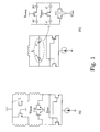
- One known approach is to use switched capacitors or inductors in a LC resonator, as shown in Fig. 1a-c [1], [2].
- the inductance or capacitance of the resonator is thus varied by utilizing switchers V switch , consequently also the oscillation frequency-band is varied.
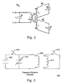
- the total inductance of the resonator can be varied by switching mutual inductance within a resonator, as shown in Fig. 2 and Fig. 3 , [3], [4].
- the document US5,138,284 discloses a push-push oscillating circuit comprising a resonator connect to a capacitor and an anti-phase combining circuit for antiphase-combining two outputs from the resonator.
- An object of the present invention is to provide an improved dual-band voltage controlled oscillator.
- a further object of the present invention is to provide a dual-band voltage controller oscillator with reduced phase noise performance.
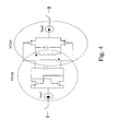
- a dual band capable voltage controlled oscillator circuit VCO comprises two voltage controlled oscillators VCO1, VCO2, wherein the voltage controlled oscillator units VCO1, VCO2 are synchronized and connected via two coupled transmission lines TL1, TL2.
- At least one switching unit is arranged across the two transmission lines to enable switching between the two modes, thereby varying a combined inductance of the synchronized oscillator units VCO1, VCO2 and thereby varying the oscillation frequency for the voltage controlled oscillator circuit VCO.
- the present invention will be discussed in the context of a general integrated circuit scheme applicable to any communication technology utilizing dual or even multiple frequency bands.
- the proposed VCO topology can be implemented in any semiconductor technology, e.g., CMOS, bipolar, Silicon, GaAs etc. It can be fully integrated on a chip but can also be made with discrete components or a mixture of ICs and discrete components.
- f 0 1 2 ⁇ ⁇ ⁇ L s , i ⁇ M ⁇ C
- the present invention generally concerns a dual-band voltage controlled oscillator VCO based on two coupled voltage controlled oscillators VCO1, VCO2.
- the two oscillators are synchronized via coupled transmission lines TL.
- the inductance of the LC resonator for each oscillator is varied, so is the oscillation frequency band for the combined voltage controlled oscillator.
- the coupled VCO:s have a better phase noise performance than known single VCO:s.
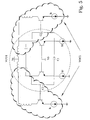
- the present invention discloses various embodiments of a general improved dual band VCO comprising at least two coupled, synchronized voltage controlled oscillators VCO1, VCO2.
- the oscillators are coupled via a mutual inductance coupled transmission line pair TL1, TL2, arranged to enable switching the operational mode of the coupled transmission line pair TL1, TL2 to provide a dual mode of operation of the voltage controlled oscillator.
- the switching action is enabled by means of switchers V switch across the coupled transmission line pair TL1, TL2.
- the respective voltage controlled oscillators VCO1 and VCO2 are represented by the negative resistor - R , and capacitor C, as well as coupled transmission lines TL1, TL2 in the proposed VCO,
- - R represents the negative resistance provided by the power amplifier of the respective voltage controlled oscillators VCO1, VCO2.
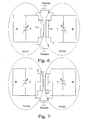
- the switchers are located at the coupled transmission lines terminals ( Fig. 6 ) or at a central portion of the coupled transmission line pair ( Fig. 7 ).
- the power amplifier preferably has sufficient gain to maintain the combined VCO oscillating at both frequency bands, e.g. both for even and odd mode.
- the thus described dual band VCO provides a voltage controlled oscillator with improved phase noise performance as compared to known solutions.
- the provided switchers control the operating mode of the coupled transmission line pair, namely, when the switcher is on, the coupled transmission line pair TL1, TL2 operates at even mode f even and the mutual inductance M is positive. Consequently, the coupled VCO works at low frequency band (see Equation 1). Opposite, when the switcher is off, the coupled transmission line pair TL1, TL2 operates in odd mode f odd and the mutual inductance M is negative. Thus, the combined VCO works in a high frequency band.
- the frequency difference between the two modes of operation is varied.
- the mutual inductance M depends on the distance between the two coupled transmission lines TL1, TL2, the length of the coupled part and the location of the transmission lines. In other words, how far apart the transmission lines are, how long the transmission lines are, and if the transmission lines are co-planar and/or stacked.
- two cross-coupled VCO:s are synchronized and coupled via a mutual inductance transmission line pair TL D .
- the switching of the operational mode of the transmission line pair TL D is enabled by means of two switchers V SWlTCH connecting respective first and second terminals of the transmission lines TL1, TL2.
- a dual-band Hartley VCO comprises two Hartley voltage controlled oscillators coupled via two pairs of transmission lines TL D , TL g , each provided with a switch V switch .
- a dual-band Colpitts VCO comprising two Colpitt voltage controlled oscillators synchronized and coupled via a coupled transmission line pair TLg.
- the operational mode of the transmission line pair is enabled using a switch connected between first terminals of the transmission line pair.
- the present invention can be applied to a dual band voltage controlled oscillator comprising at least two Clapp VCO:s. Because all the above VCO:s have a LC resonator, the inductor or a part of an inductor can be coupled, to build a dual-band VCO.
- the general concept of the present invention can be used to construct differential VCO:s, to provide differential signals regardless of the operational mode of the coupled transmission lines.
- the example as shown in Fig. 10 , is based on two synchronized dual-band Colpitts VCO according to the present invention, each comprising two synchronized Colpitt VCO:s and a coupled transmission line pair TLg and switches at said transmission lines.
- transistors M1 and M2 always operate differentially and the differential signal can be provided at their base or emitter.
- the cross-coupled dual-band VCO disclosed in Fig. 8 can be arranged to deliver a differential signal.
- the power amplifier gain for each VCO is switched or varied between different frequency bands.
- the combined VCO can be forced to oscillate at only one frequency band. Since at this oscillation frequency band only the VCO:s loop gain can be larger than or equal to 1 to fulfill the oscillation condition. That frequency corresponds to one operational mode of the coupled transmission lines. At another oscillation frequency band or transmission line operational mode, the power gain is too small to provide the VCO oscillation.
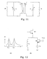
- FIG. 11 A simplified schematic of the proposed amplifier gain switching solution is illustrated in Fig. 11 .
- a dual-band amplifier is required for each voltage controlled oscillator VCO1 , VCO2, in order to provide a power gain to maintain the combined VCO operating at one frequency band, as shown in the diagram in Fig. 12a .
- any dual-band amplifier can be used, provided that it can be switched.
- Fig. 12b a switched dual-band amplifier is illustrated, where the switched source degeneration is used to control the gain at different frequency bands.
- the resonator when switcher M2 is on, the resonator has the largest impedance at f even and causes the amplifier to have its lowest gain at f even .
- the resonator becomes capacitive with a quite low impedance, and consequently the amplifier has a high gain.
- the voltage controlled oscillator will operate at f odd , high frequency band.
- the inductor Ls when switching M2 off, the inductor Ls becomes the source degeneration whose impedance increases with frequency, therefore the amplifier exhibits high gain at f even and low gain at f odd . In this case, the VCO will oscillate at f even low frequency band.
- the dual band switching of the proposed VCO is realized by altering the frequency response of the amplifier gain.
- this can be applied to different VCO topologies.
- the concept can be applied to the same set up of synchronized voltage controlled oscillators as described with reference to Figs. 8-10 , but without the provided switches at the transmission lines. Instead the switching is provided via switched power amplifiers provided at the respective VCO:s.
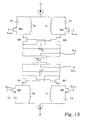
- a dual-band cross coupled VCO Fig. 13
- a dual-band Hartley VCO Fig. 14a
- a dual-band Colpitts VCO Fig. 14b
- the proposed dual-band VCO can be used to construct differential VOC:s, to generate differential signals for both transmission lines modes.
- two dual-band Colpitts VCO are synchronized and the differential signal can be taken from the base or emitter of transistors M1 and M2.
- the dual-band cross-coupled VCO in Fig. 13 can be utilized to provide differential signals.
- the switcher When using the dual-band switched power amplifier, the switcher itself is not a part of VCO's resonator. Consequently, the VCO's phase noise does not sensitive to the switcher's parasitic resistance and capacitance.
- Mutual inductance M is the concept that the current through one inductor can induce a voltage in another nearby inductor. It is important as the mechanism by which transformers work, but it can also cause coupling between conductors in a circuit.
- the mutual inductance M is also a measure of the coupling between two inductors.
Landscapes
- Engineering & Computer Science (AREA)
- Power Engineering (AREA)
- Inductance-Capacitance Distribution Constants And Capacitance-Resistance Oscillators (AREA)
Claims (3)
- Zweibandfähige spannungsgesteuerte Oszillatorschaltung (VCO), die zwei spannungsgesteuerte Oszillator-Baugruppen (VCO1, VCO2) umfasst, die durch zwei miteinander gekoppelte Übertragungsleitungen (TL1, TL2) synchronisiert und verbunden sind, wobei die Übertragungsleitungen (TL1, TL2) derart angeordnet sind, dass sie nach einem der zwei Modi, nämlich einem Gleichtaktmodus und einem Gegentaktmodus arbeiten, wobei die Gesamtinduktivität jeder Übertragungsleitung, Li, im Gleichtaktmodus Li = Ls,i + M und im Gegentaktmodus Li = Ls,i - M ist, wobei Ls,i die Eigeninduktion jeder Übertragungsleitung darstellt, i = 1, 2 und M ist die gegenseitige Induktivität,
gekennzeichnet durch
mindestens eine Schalteinheit, die quer über den Übertragungsleitungen angeordnet ist, um das Schalten zwischen den zwei Modi zu ermöglichen, und dabei eine kombinierte Induktivität der synchronisierten Oszillator-Baugruppen (VCO1, VCO2) und der Schwingungszahl für die spannungsgesteuerte Oszillatorschaltung (VCO) zu variieren. - Schaltung nach Anspruch 1, gekennzeichnet durch zwei Schalteinheiten (Vswitch), die an den jeweiligen ersten und zweiten Klemmen der gekoppelten Übertragungsleitungen (TL1, TL2) angeordnet sind und diese verbinden.
- Schaltung nach Anspruch 1, gekennzeichnet durch mindestens eine Schalteinheit, die derart angeordnet ist, dass sie einen Mittelabschnitt von jeder der gekoppelten Übertragungsleitungen verbindet.
Applications Claiming Priority (1)
| Application Number | Priority Date | Filing Date | Title |
|---|---|---|---|
| PCT/SE2007/050770 WO2009054760A1 (en) | 2007-10-23 | 2007-10-23 | A dual-band coupled vco |
Publications (3)
| Publication Number | Publication Date |
|---|---|
| EP2201676A1 EP2201676A1 (de) | 2010-06-30 |
| EP2201676A4 EP2201676A4 (de) | 2012-11-28 |
| EP2201676B1 true EP2201676B1 (de) | 2014-06-04 |
Family
ID=40579750
Family Applications (1)
| Application Number | Title | Priority Date | Filing Date |
|---|---|---|---|
| EP07835354.7A Not-in-force EP2201676B1 (de) | 2007-10-23 | 2007-10-23 | Zweibandgekoppelter vco |
Country Status (4)
| Country | Link |
|---|---|
| US (1) | US8125282B2 (de) |
| EP (1) | EP2201676B1 (de) |
| JP (1) | JP5302323B2 (de) |
| WO (1) | WO2009054760A1 (de) |
Families Citing this family (148)
| Publication number | Priority date | Publication date | Assignee | Title |
|---|---|---|---|---|
| US8058934B2 (en) * | 2009-06-03 | 2011-11-15 | Qualcomm Incorporated | Apparatus and method for frequency generation |
| FR2962612B1 (fr) | 2010-07-06 | 2013-03-29 | St Microelectronics Sa | Oscillateur commande en tension multi-bande sans capacite commutee. |
| FR2969428B1 (fr) * | 2010-12-21 | 2013-01-04 | St Microelectronics Sa | Commutateur electronique et appareil de communication incluant un tel commutateur |
| US8294528B2 (en) * | 2010-12-28 | 2012-10-23 | Qualcomm Incorporated | Wideband multi-mode VCO |
| US9954488B2 (en) | 2013-03-15 | 2018-04-24 | Taiwan Semiconductor Manufacturing Company, Ltd. | Varainductor, voltage controlled oscillator including the varainductor, and phase locked loop including the varainductor |
| US8988158B2 (en) * | 2013-03-15 | 2015-03-24 | Qualcomm Incorporated | Hybrid voltage controlled oscillator |
| US9240752B2 (en) | 2013-03-26 | 2016-01-19 | Stmicroelectronics S.R.L. | Power oscillator apparatus with transformer-based power combining |
| US9306614B2 (en) | 2013-03-26 | 2016-04-05 | Stmicroelectronics S.R.L. | Power oscillator apparatus with transformer-based power combining for galvanically-isolated bidirectional data communication and power transfer |
| US9999038B2 (en) | 2013-05-31 | 2018-06-12 | At&T Intellectual Property I, L.P. | Remote distributed antenna system |
| US9525524B2 (en) | 2013-05-31 | 2016-12-20 | At&T Intellectual Property I, L.P. | Remote distributed antenna system |
| US8897697B1 (en) | 2013-11-06 | 2014-11-25 | At&T Intellectual Property I, Lp | Millimeter-wave surface-wave communications |
| US9362893B2 (en) | 2014-06-23 | 2016-06-07 | Analog Devices, Inc. | Apparatus and methods for switch-coupled oscillators |
| US9768833B2 (en) | 2014-09-15 | 2017-09-19 | At&T Intellectual Property I, L.P. | Method and apparatus for sensing a condition in a transmission medium of electromagnetic waves |
| US10063280B2 (en) | 2014-09-17 | 2018-08-28 | At&T Intellectual Property I, L.P. | Monitoring and mitigating conditions in a communication network |
| US9615269B2 (en) | 2014-10-02 | 2017-04-04 | At&T Intellectual Property I, L.P. | Method and apparatus that provides fault tolerance in a communication network |
| US9685992B2 (en) | 2014-10-03 | 2017-06-20 | At&T Intellectual Property I, L.P. | Circuit panel network and methods thereof |
| US9503189B2 (en) | 2014-10-10 | 2016-11-22 | At&T Intellectual Property I, L.P. | Method and apparatus for arranging communication sessions in a communication system |
| KR101668158B1 (ko) * | 2014-10-14 | 2016-10-21 | 숭실대학교산학협력단 | 발진기를 이용한 칩 간 무선 전력 전송 장치 |
| US9762289B2 (en) | 2014-10-14 | 2017-09-12 | At&T Intellectual Property I, L.P. | Method and apparatus for transmitting or receiving signals in a transportation system |
| US9973299B2 (en) | 2014-10-14 | 2018-05-15 | At&T Intellectual Property I, L.P. | Method and apparatus for adjusting a mode of communication in a communication network |
| US9577306B2 (en) | 2014-10-21 | 2017-02-21 | At&T Intellectual Property I, L.P. | Guided-wave transmission device and methods for use therewith |
| US9312919B1 (en) | 2014-10-21 | 2016-04-12 | At&T Intellectual Property I, Lp | Transmission device with impairment compensation and methods for use therewith |
| US9769020B2 (en) | 2014-10-21 | 2017-09-19 | At&T Intellectual Property I, L.P. | Method and apparatus for responding to events affecting communications in a communication network |
| US9653770B2 (en) | 2014-10-21 | 2017-05-16 | At&T Intellectual Property I, L.P. | Guided wave coupler, coupling module and methods for use therewith |
| US9780834B2 (en) | 2014-10-21 | 2017-10-03 | At&T Intellectual Property I, L.P. | Method and apparatus for transmitting electromagnetic waves |
| US9627768B2 (en) | 2014-10-21 | 2017-04-18 | At&T Intellectual Property I, L.P. | Guided-wave transmission device with non-fundamental mode propagation and methods for use therewith |
| CN105577118B (zh) * | 2014-11-03 | 2019-05-21 | 联咏科技股份有限公司 | 振荡器、时脉产生器以及时脉信号的产生方法 |
| US10340573B2 (en) | 2016-10-26 | 2019-07-02 | At&T Intellectual Property I, L.P. | Launcher with cylindrical coupling device and methods for use therewith |
| US9742462B2 (en) | 2014-12-04 | 2017-08-22 | At&T Intellectual Property I, L.P. | Transmission medium and communication interfaces and methods for use therewith |
| US9461706B1 (en) | 2015-07-31 | 2016-10-04 | At&T Intellectual Property I, Lp | Method and apparatus for exchanging communication signals |
| US9800327B2 (en) | 2014-11-20 | 2017-10-24 | At&T Intellectual Property I, L.P. | Apparatus for controlling operations of a communication device and methods thereof |
| US10009067B2 (en) | 2014-12-04 | 2018-06-26 | At&T Intellectual Property I, L.P. | Method and apparatus for configuring a communication interface |
| US9997819B2 (en) | 2015-06-09 | 2018-06-12 | At&T Intellectual Property I, L.P. | Transmission medium and method for facilitating propagation of electromagnetic waves via a core |
| US9544006B2 (en) | 2014-11-20 | 2017-01-10 | At&T Intellectual Property I, L.P. | Transmission device with mode division multiplexing and methods for use therewith |
| US10243784B2 (en) | 2014-11-20 | 2019-03-26 | At&T Intellectual Property I, L.P. | System for generating topology information and methods thereof |
| US9954287B2 (en) | 2014-11-20 | 2018-04-24 | At&T Intellectual Property I, L.P. | Apparatus for converting wireless signals and electromagnetic waves and methods thereof |
| US9876570B2 (en) | 2015-02-20 | 2018-01-23 | At&T Intellectual Property I, Lp | Guided-wave transmission device with non-fundamental mode propagation and methods for use therewith |
| US9749013B2 (en) | 2015-03-17 | 2017-08-29 | At&T Intellectual Property I, L.P. | Method and apparatus for reducing attenuation of electromagnetic waves guided by a transmission medium |
| US9543891B2 (en) * | 2015-04-09 | 2017-01-10 | Texas Instruments Incorporated | Low-power low-phase-noise oscillator |
| US9705561B2 (en) | 2015-04-24 | 2017-07-11 | At&T Intellectual Property I, L.P. | Directional coupling device and methods for use therewith |
| US10224981B2 (en) | 2015-04-24 | 2019-03-05 | At&T Intellectual Property I, Lp | Passive electrical coupling device and methods for use therewith |
| US9948354B2 (en) | 2015-04-28 | 2018-04-17 | At&T Intellectual Property I, L.P. | Magnetic coupling device with reflective plate and methods for use therewith |
| US9793954B2 (en) | 2015-04-28 | 2017-10-17 | At&T Intellectual Property I, L.P. | Magnetic coupling device and methods for use therewith |
| US9490869B1 (en) | 2015-05-14 | 2016-11-08 | At&T Intellectual Property I, L.P. | Transmission medium having multiple cores and methods for use therewith |
| US9748626B2 (en) | 2015-05-14 | 2017-08-29 | At&T Intellectual Property I, L.P. | Plurality of cables having different cross-sectional shapes which are bundled together to form a transmission medium |
| US9871282B2 (en) | 2015-05-14 | 2018-01-16 | At&T Intellectual Property I, L.P. | At least one transmission medium having a dielectric surface that is covered at least in part by a second dielectric |
| US10650940B2 (en) | 2015-05-15 | 2020-05-12 | At&T Intellectual Property I, L.P. | Transmission medium having a conductive material and methods for use therewith |
| US9917341B2 (en) | 2015-05-27 | 2018-03-13 | At&T Intellectual Property I, L.P. | Apparatus and method for launching electromagnetic waves and for modifying radial dimensions of the propagating electromagnetic waves |
| US9912381B2 (en) | 2015-06-03 | 2018-03-06 | At&T Intellectual Property I, Lp | Network termination and methods for use therewith |
| US9866309B2 (en) | 2015-06-03 | 2018-01-09 | At&T Intellectual Property I, Lp | Host node device and methods for use therewith |
| US10812174B2 (en) | 2015-06-03 | 2020-10-20 | At&T Intellectual Property I, L.P. | Client node device and methods for use therewith |
| US9913139B2 (en) | 2015-06-09 | 2018-03-06 | At&T Intellectual Property I, L.P. | Signal fingerprinting for authentication of communicating devices |
| US9608692B2 (en) | 2015-06-11 | 2017-03-28 | At&T Intellectual Property I, L.P. | Repeater and methods for use therewith |
| US9820146B2 (en) | 2015-06-12 | 2017-11-14 | At&T Intellectual Property I, L.P. | Method and apparatus for authentication and identity management of communicating devices |
| US9667317B2 (en) | 2015-06-15 | 2017-05-30 | At&T Intellectual Property I, L.P. | Method and apparatus for providing security using network traffic adjustments |
| US9819307B2 (en) | 2015-06-19 | 2017-11-14 | Qualcomm Incorporated | Low power current re-using transformer-based dual-band voltage controlled oscillator |
| US9865911B2 (en) | 2015-06-25 | 2018-01-09 | At&T Intellectual Property I, L.P. | Waveguide system for slot radiating first electromagnetic waves that are combined into a non-fundamental wave mode second electromagnetic wave on a transmission medium |
| US9509415B1 (en) | 2015-06-25 | 2016-11-29 | At&T Intellectual Property I, L.P. | Methods and apparatus for inducing a fundamental wave mode on a transmission medium |
| US9640850B2 (en) | 2015-06-25 | 2017-05-02 | At&T Intellectual Property I, L.P. | Methods and apparatus for inducing a non-fundamental wave mode on a transmission medium |
| US9882257B2 (en) | 2015-07-14 | 2018-01-30 | At&T Intellectual Property I, L.P. | Method and apparatus for launching a wave mode that mitigates interference |
| US9847566B2 (en) | 2015-07-14 | 2017-12-19 | At&T Intellectual Property I, L.P. | Method and apparatus for adjusting a field of a signal to mitigate interference |
| US9628116B2 (en) | 2015-07-14 | 2017-04-18 | At&T Intellectual Property I, L.P. | Apparatus and methods for transmitting wireless signals |
| US10170840B2 (en) | 2015-07-14 | 2019-01-01 | At&T Intellectual Property I, L.P. | Apparatus and methods for sending or receiving electromagnetic signals |
| US10033108B2 (en) | 2015-07-14 | 2018-07-24 | At&T Intellectual Property I, L.P. | Apparatus and methods for generating an electromagnetic wave having a wave mode that mitigates interference |
| US10320586B2 (en) | 2015-07-14 | 2019-06-11 | At&T Intellectual Property I, L.P. | Apparatus and methods for generating non-interfering electromagnetic waves on an insulated transmission medium |
| US10341142B2 (en) | 2015-07-14 | 2019-07-02 | At&T Intellectual Property I, L.P. | Apparatus and methods for generating non-interfering electromagnetic waves on an uninsulated conductor |
| US10044409B2 (en) | 2015-07-14 | 2018-08-07 | At&T Intellectual Property I, L.P. | Transmission medium and methods for use therewith |
| US10205655B2 (en) | 2015-07-14 | 2019-02-12 | At&T Intellectual Property I, L.P. | Apparatus and methods for communicating utilizing an antenna array and multiple communication paths |
| US9722318B2 (en) | 2015-07-14 | 2017-08-01 | At&T Intellectual Property I, L.P. | Method and apparatus for coupling an antenna to a device |
| US10148016B2 (en) | 2015-07-14 | 2018-12-04 | At&T Intellectual Property I, L.P. | Apparatus and methods for communicating utilizing an antenna array |
| US9853342B2 (en) | 2015-07-14 | 2017-12-26 | At&T Intellectual Property I, L.P. | Dielectric transmission medium connector and methods for use therewith |
| US10090606B2 (en) | 2015-07-15 | 2018-10-02 | At&T Intellectual Property I, L.P. | Antenna system with dielectric array and methods for use therewith |
| US9793951B2 (en) | 2015-07-15 | 2017-10-17 | At&T Intellectual Property I, L.P. | Method and apparatus for launching a wave mode that mitigates interference |
| US9871283B2 (en) | 2015-07-23 | 2018-01-16 | At&T Intellectual Property I, Lp | Transmission medium having a dielectric core comprised of plural members connected by a ball and socket configuration |
| US9749053B2 (en) | 2015-07-23 | 2017-08-29 | At&T Intellectual Property I, L.P. | Node device, repeater and methods for use therewith |
| US9912027B2 (en) | 2015-07-23 | 2018-03-06 | At&T Intellectual Property I, L.P. | Method and apparatus for exchanging communication signals |
| US9948333B2 (en) | 2015-07-23 | 2018-04-17 | At&T Intellectual Property I, L.P. | Method and apparatus for wireless communications to mitigate interference |
| US9967173B2 (en) | 2015-07-31 | 2018-05-08 | At&T Intellectual Property I, L.P. | Method and apparatus for authentication and identity management of communicating devices |
| US9735833B2 (en) | 2015-07-31 | 2017-08-15 | At&T Intellectual Property I, L.P. | Method and apparatus for communications management in a neighborhood network |
| US9904535B2 (en) | 2015-09-14 | 2018-02-27 | At&T Intellectual Property I, L.P. | Method and apparatus for distributing software |
| US9769128B2 (en) | 2015-09-28 | 2017-09-19 | At&T Intellectual Property I, L.P. | Method and apparatus for encryption of communications over a network |
| US9729197B2 (en) | 2015-10-01 | 2017-08-08 | At&T Intellectual Property I, L.P. | Method and apparatus for communicating network management traffic over a network |
| US9876264B2 (en) | 2015-10-02 | 2018-01-23 | At&T Intellectual Property I, Lp | Communication system, guided wave switch and methods for use therewith |
| US10355367B2 (en) | 2015-10-16 | 2019-07-16 | At&T Intellectual Property I, L.P. | Antenna structure for exchanging wireless signals |
| WO2018038651A1 (en) * | 2016-08-23 | 2018-03-01 | Telefonaktiebolaget Lm Ericsson (Publ) | Biasing circuit for capacitor switch transistor and method therefore |
| US9860075B1 (en) | 2016-08-26 | 2018-01-02 | At&T Intellectual Property I, L.P. | Method and communication node for broadband distribution |
| US10291311B2 (en) | 2016-09-09 | 2019-05-14 | At&T Intellectual Property I, L.P. | Method and apparatus for mitigating a fault in a distributed antenna system |
| US11032819B2 (en) | 2016-09-15 | 2021-06-08 | At&T Intellectual Property I, L.P. | Method and apparatus for use with a radio distributed antenna system having a control channel reference signal |
| US10135147B2 (en) | 2016-10-18 | 2018-11-20 | At&T Intellectual Property I, L.P. | Apparatus and methods for launching guided waves via an antenna |
| US10135146B2 (en) | 2016-10-18 | 2018-11-20 | At&T Intellectual Property I, L.P. | Apparatus and methods for launching guided waves via circuits |
| US10340600B2 (en) | 2016-10-18 | 2019-07-02 | At&T Intellectual Property I, L.P. | Apparatus and methods for launching guided waves via plural waveguide systems |
| US10374316B2 (en) | 2016-10-21 | 2019-08-06 | At&T Intellectual Property I, L.P. | System and dielectric antenna with non-uniform dielectric |
| US9876605B1 (en) | 2016-10-21 | 2018-01-23 | At&T Intellectual Property I, L.P. | Launcher and coupling system to support desired guided wave mode |
| US9991580B2 (en) | 2016-10-21 | 2018-06-05 | At&T Intellectual Property I, L.P. | Launcher and coupling system for guided wave mode cancellation |
| US10811767B2 (en) | 2016-10-21 | 2020-10-20 | At&T Intellectual Property I, L.P. | System and dielectric antenna with convex dielectric radome |
| US10312567B2 (en) | 2016-10-26 | 2019-06-04 | At&T Intellectual Property I, L.P. | Launcher with planar strip antenna and methods for use therewith |
| US10225025B2 (en) | 2016-11-03 | 2019-03-05 | At&T Intellectual Property I, L.P. | Method and apparatus for detecting a fault in a communication system |
| US10224634B2 (en) | 2016-11-03 | 2019-03-05 | At&T Intellectual Property I, L.P. | Methods and apparatus for adjusting an operational characteristic of an antenna |
| US10498044B2 (en) | 2016-11-03 | 2019-12-03 | At&T Intellectual Property I, L.P. | Apparatus for configuring a surface of an antenna |
| US10291334B2 (en) | 2016-11-03 | 2019-05-14 | At&T Intellectual Property I, L.P. | System for detecting a fault in a communication system |
| CN106571777A (zh) * | 2016-11-04 | 2017-04-19 | 华为技术有限公司 | 双模振荡器及多相位振荡器 |
| US10178445B2 (en) | 2016-11-23 | 2019-01-08 | At&T Intellectual Property I, L.P. | Methods, devices, and systems for load balancing between a plurality of waveguides |
| US10340601B2 (en) | 2016-11-23 | 2019-07-02 | At&T Intellectual Property I, L.P. | Multi-antenna system and methods for use therewith |
| US10340603B2 (en) | 2016-11-23 | 2019-07-02 | At&T Intellectual Property I, L.P. | Antenna system having shielded structural configurations for assembly |
| US10535928B2 (en) | 2016-11-23 | 2020-01-14 | At&T Intellectual Property I, L.P. | Antenna system and methods for use therewith |
| US10090594B2 (en) | 2016-11-23 | 2018-10-02 | At&T Intellectual Property I, L.P. | Antenna system having structural configurations for assembly |
| US10361489B2 (en) | 2016-12-01 | 2019-07-23 | At&T Intellectual Property I, L.P. | Dielectric dish antenna system and methods for use therewith |
| US10305190B2 (en) | 2016-12-01 | 2019-05-28 | At&T Intellectual Property I, L.P. | Reflecting dielectric antenna system and methods for use therewith |
| US10727599B2 (en) | 2016-12-06 | 2020-07-28 | At&T Intellectual Property I, L.P. | Launcher with slot antenna and methods for use therewith |
| US10326494B2 (en) | 2016-12-06 | 2019-06-18 | At&T Intellectual Property I, L.P. | Apparatus for measurement de-embedding and methods for use therewith |
| US10135145B2 (en) | 2016-12-06 | 2018-11-20 | At&T Intellectual Property I, L.P. | Apparatus and methods for generating an electromagnetic wave along a transmission medium |
| US10382976B2 (en) | 2016-12-06 | 2019-08-13 | At&T Intellectual Property I, L.P. | Method and apparatus for managing wireless communications based on communication paths and network device positions |
| US10637149B2 (en) | 2016-12-06 | 2020-04-28 | At&T Intellectual Property I, L.P. | Injection molded dielectric antenna and methods for use therewith |
| US10755542B2 (en) | 2016-12-06 | 2020-08-25 | At&T Intellectual Property I, L.P. | Method and apparatus for surveillance via guided wave communication |
| US10439675B2 (en) | 2016-12-06 | 2019-10-08 | At&T Intellectual Property I, L.P. | Method and apparatus for repeating guided wave communication signals |
| US10694379B2 (en) | 2016-12-06 | 2020-06-23 | At&T Intellectual Property I, L.P. | Waveguide system with device-based authentication and methods for use therewith |
| US10819035B2 (en) | 2016-12-06 | 2020-10-27 | At&T Intellectual Property I, L.P. | Launcher with helical antenna and methods for use therewith |
| US10020844B2 (en) | 2016-12-06 | 2018-07-10 | T&T Intellectual Property I, L.P. | Method and apparatus for broadcast communication via guided waves |
| US9927517B1 (en) | 2016-12-06 | 2018-03-27 | At&T Intellectual Property I, L.P. | Apparatus and methods for sensing rainfall |
| US10139820B2 (en) | 2016-12-07 | 2018-11-27 | At&T Intellectual Property I, L.P. | Method and apparatus for deploying equipment of a communication system |
| US10446936B2 (en) | 2016-12-07 | 2019-10-15 | At&T Intellectual Property I, L.P. | Multi-feed dielectric antenna system and methods for use therewith |
| US10243270B2 (en) | 2016-12-07 | 2019-03-26 | At&T Intellectual Property I, L.P. | Beam adaptive multi-feed dielectric antenna system and methods for use therewith |
| US10359749B2 (en) | 2016-12-07 | 2019-07-23 | At&T Intellectual Property I, L.P. | Method and apparatus for utilities management via guided wave communication |
| US10027397B2 (en) | 2016-12-07 | 2018-07-17 | At&T Intellectual Property I, L.P. | Distributed antenna system and methods for use therewith |
| US9893795B1 (en) | 2016-12-07 | 2018-02-13 | At&T Intellectual Property I, Lp | Method and repeater for broadband distribution |
| US10389029B2 (en) | 2016-12-07 | 2019-08-20 | At&T Intellectual Property I, L.P. | Multi-feed dielectric antenna system with core selection and methods for use therewith |
| US10547348B2 (en) | 2016-12-07 | 2020-01-28 | At&T Intellectual Property I, L.P. | Method and apparatus for switching transmission mediums in a communication system |
| US10168695B2 (en) | 2016-12-07 | 2019-01-01 | At&T Intellectual Property I, L.P. | Method and apparatus for controlling an unmanned aircraft |
| US10601494B2 (en) | 2016-12-08 | 2020-03-24 | At&T Intellectual Property I, L.P. | Dual-band communication device and method for use therewith |
| US10411356B2 (en) | 2016-12-08 | 2019-09-10 | At&T Intellectual Property I, L.P. | Apparatus and methods for selectively targeting communication devices with an antenna array |
| US10530505B2 (en) | 2016-12-08 | 2020-01-07 | At&T Intellectual Property I, L.P. | Apparatus and methods for launching electromagnetic waves along a transmission medium |
| US10916969B2 (en) | 2016-12-08 | 2021-02-09 | At&T Intellectual Property I, L.P. | Method and apparatus for providing power using an inductive coupling |
| US10326689B2 (en) | 2016-12-08 | 2019-06-18 | At&T Intellectual Property I, L.P. | Method and system for providing alternative communication paths |
| US10069535B2 (en) | 2016-12-08 | 2018-09-04 | At&T Intellectual Property I, L.P. | Apparatus and methods for launching electromagnetic waves having a certain electric field structure |
| US9998870B1 (en) | 2016-12-08 | 2018-06-12 | At&T Intellectual Property I, L.P. | Method and apparatus for proximity sensing |
| US9911020B1 (en) | 2016-12-08 | 2018-03-06 | At&T Intellectual Property I, L.P. | Method and apparatus for tracking via a radio frequency identification device |
| US10103422B2 (en) | 2016-12-08 | 2018-10-16 | At&T Intellectual Property I, L.P. | Method and apparatus for mounting network devices |
| US10777873B2 (en) | 2016-12-08 | 2020-09-15 | At&T Intellectual Property I, L.P. | Method and apparatus for mounting network devices |
| US10389037B2 (en) | 2016-12-08 | 2019-08-20 | At&T Intellectual Property I, L.P. | Apparatus and methods for selecting sections of an antenna array and use therewith |
| US10938108B2 (en) | 2016-12-08 | 2021-03-02 | At&T Intellectual Property I, L.P. | Frequency selective multi-feed dielectric antenna system and methods for use therewith |
| US9838896B1 (en) | 2016-12-09 | 2017-12-05 | At&T Intellectual Property I, L.P. | Method and apparatus for assessing network coverage |
| US10340983B2 (en) | 2016-12-09 | 2019-07-02 | At&T Intellectual Property I, L.P. | Method and apparatus for surveying remote sites via guided wave communications |
| US10264586B2 (en) | 2016-12-09 | 2019-04-16 | At&T Mobility Ii Llc | Cloud-based packet controller and methods for use therewith |
| US9973940B1 (en) | 2017-02-27 | 2018-05-15 | At&T Intellectual Property I, L.P. | Apparatus and methods for dynamic impedance matching of a guided wave launcher |
| US10298293B2 (en) | 2017-03-13 | 2019-05-21 | At&T Intellectual Property I, L.P. | Apparatus of communication utilizing wireless network devices |
| CN112970181B (zh) | 2018-12-26 | 2022-08-09 | 华为技术有限公司 | 一种包含谐振电路的集成电路 |
| US11239794B2 (en) * | 2020-06-10 | 2022-02-01 | Intel Corporation | Coupled frequency doubler with frequency tracking loop |
| US11575359B2 (en) | 2021-04-21 | 2023-02-07 | Cisco Technology, Inc. | Multi-port coupled inductor with interference suppression |
Family Cites Families (9)
| Publication number | Priority date | Publication date | Assignee | Title |
|---|---|---|---|---|
| US3624514A (en) * | 1970-01-09 | 1971-11-30 | Philips Corp | Tuning circuit having common tuning element for three frequency ranges and self-oscillating mixer using same |
| JP2507181B2 (ja) * | 1990-06-29 | 1996-06-12 | 松下電器産業株式会社 | プッシュプッシュ発振器 |
| US5629652A (en) * | 1996-05-09 | 1997-05-13 | Analog Devices | Band-switchable, low-noise voltage controlled oscillator (VCO) for use with low-q resonator elements |
| SE0102420D0 (sv) * | 2001-07-05 | 2001-07-05 | Ericsson Telefon Ab L M | Oscillator |
| US7005930B1 (en) * | 2001-11-14 | 2006-02-28 | Berkana Wireless, Inc. | Synchronously coupled oscillator |
| US7098737B2 (en) * | 2002-05-31 | 2006-08-29 | Kabushiki Kaisha Toshiba | Variable inductor, oscillator including the variable inductor and radio terminal comprising this oscillator, and amplifier including the variable inductor and radio terminal comprising this amplifier |
| US6943635B1 (en) * | 2003-09-30 | 2005-09-13 | Conexant Systems, Inc. | Optimum RF VCO structure |
| US7154349B2 (en) * | 2004-08-11 | 2006-12-26 | Qualcomm, Incorporated | Coupled-inductor multi-band VCO |
| US7423495B2 (en) * | 2006-06-26 | 2008-09-09 | Infineon Technologies Ag | Oscillator and method for generating an oscillator signal |
-
2007
- 2007-10-23 US US12/739,012 patent/US8125282B2/en not_active Expired - Fee Related
- 2007-10-23 EP EP07835354.7A patent/EP2201676B1/de not_active Not-in-force
- 2007-10-23 JP JP2010530953A patent/JP5302323B2/ja not_active Expired - Fee Related
- 2007-10-23 WO PCT/SE2007/050770 patent/WO2009054760A1/en not_active Ceased
Also Published As
| Publication number | Publication date |
|---|---|
| WO2009054760A1 (en) | 2009-04-30 |
| EP2201676A1 (de) | 2010-06-30 |
| US8125282B2 (en) | 2012-02-28 |
| JP2011501608A (ja) | 2011-01-06 |
| US20100271086A1 (en) | 2010-10-28 |
| JP5302323B2 (ja) | 2013-10-02 |
| EP2201676A4 (de) | 2012-11-28 |
Similar Documents
| Publication | Publication Date | Title |
|---|---|---|
| EP2201676B1 (de) | Zweibandgekoppelter vco | |
| Tiebout | Low-power low-phase-noise differentially tuned quadrature VCO design in standard CMOS | |
| EP2289164B1 (de) | Spannungsgesteuerte zweiband-oszillatoranordnung | |
| EP1929486B1 (de) | Variable integrierte induktivität | |
| US20080284534A1 (en) | Oscillator | |
| US20060028283A1 (en) | Symmetrical linear voltage controlled oscillator | |
| US20090302958A1 (en) | Digitally controlled oscillator and phase locked loop circuit using the digitally controlled oscillator | |
| EP3158640B1 (de) | Funkfrequenzoszillator | |
| US20090289727A1 (en) | Oscillator for generating different oscillations | |
| US8665030B2 (en) | Voltage-controlled oscillator | |
| US6661301B2 (en) | Oscillator circuit | |
| EP1589655B1 (de) | Spannungsgesteuerter Breitbandozzillator mit gekoppelten Resonatoren vom Dämpfungstyp | |
| EP1552601B1 (de) | Oszillatoren mit kreisförmiger geometrie | |
| EP1542354B1 (de) | Spannungsgesteuerter-, Push-push-, Breitband-, Mikrowellenoszillator mit sehr niedrigem Rausch | |
| Sapone et al. | A 0.13-$\mu {\hbox {m}} $ SiGe BiCMOS Colpitts-Based VCO for $ W $-Band Radar Transmitters | |
| US7286024B2 (en) | Voltage-controlled oscillator with differential output | |
| EP1563599B1 (de) | Oszillatoranordnung für sehr niedrige phasenrauschwirkung | |
| CN102577098B (zh) | 振荡器、频率合成器和用于在电信网络中使用的网络节点 | |
| EP1628390B1 (de) | Spannungsgesteuerter Breitbandoszillator or mit niedrigem Phasenrausch und einen abstimmbaren Hybridnetzwerk | |
| US20050084053A1 (en) | Tunable oscillator | |
| Catli et al. | A 0.5-V 3.6/5.2 GHz CMOS multi-band LC VCO for ultra low-voltage wireless applications | |
| JP2012253561A (ja) | 電圧制御発振器 | |
| Jacobsson et al. | Low phase noise sub-1 V supply 12 and 18 GHz VCOs in 90 nm CMOS | |
| Çatlı et al. | Dual-band ultra-wide tuning range CMOS voltage-controlled oscillator | |
| EP1515427B1 (de) | Breitbandstimmbarer spannungsgesteuerter Oszillator |
Legal Events
| Date | Code | Title | Description |
|---|---|---|---|
| PUAI | Public reference made under article 153(3) epc to a published international application that has entered the european phase |
Free format text: ORIGINAL CODE: 0009012 |
|
| 17P | Request for examination filed |
Effective date: 20100316 |
|
| AK | Designated contracting states |
Kind code of ref document: A1 Designated state(s): AT BE BG CH CY CZ DE DK EE ES FI FR GB GR HU IE IS IT LI LT LU LV MC MT NL PL PT RO SE SI SK TR |
|
| AX | Request for extension of the european patent |
Extension state: AL BA HR MK RS |
|
| DAX | Request for extension of the european patent (deleted) | ||
| A4 | Supplementary search report drawn up and despatched |
Effective date: 20121025 |
|
| RIC1 | Information provided on ipc code assigned before grant |
Ipc: H03B 5/18 20060101ALI20121019BHEP Ipc: H03B 5/12 20060101AFI20121019BHEP |
|
| GRAP | Despatch of communication of intention to grant a patent |
Free format text: ORIGINAL CODE: EPIDOSNIGR1 |
|
| INTG | Intention to grant announced |
Effective date: 20140107 |
|
| GRAS | Grant fee paid |
Free format text: ORIGINAL CODE: EPIDOSNIGR3 |
|
| GRAA | (expected) grant |
Free format text: ORIGINAL CODE: 0009210 |
|
| AK | Designated contracting states |
Kind code of ref document: B1 Designated state(s): AT BE BG CH CY CZ DE DK EE ES FI FR GB GR HU IE IS IT LI LT LU LV MC MT NL PL PT RO SE SI SK TR |
|
| REG | Reference to a national code |
Ref country code: GB Ref legal event code: FG4D |
|
| REG | Reference to a national code |
Ref country code: CH Ref legal event code: EP |
|
| REG | Reference to a national code |
Ref country code: AT Ref legal event code: REF Ref document number: 671579 Country of ref document: AT Kind code of ref document: T Effective date: 20140615 |
|
| REG | Reference to a national code |
Ref country code: IE Ref legal event code: FG4D |
|
| REG | Reference to a national code |
Ref country code: DE Ref legal event code: R096 Ref document number: 602007037042 Country of ref document: DE Effective date: 20140717 |
|
| REG | Reference to a national code |
Ref country code: DE Ref legal event code: R082 Ref document number: 602007037042 Country of ref document: DE Representative=s name: GRUENECKER, KINKELDEY, STOCKMAIR & SCHWANHAEUS, DE |
|
| REG | Reference to a national code |
Ref country code: AT Ref legal event code: MK05 Ref document number: 671579 Country of ref document: AT Kind code of ref document: T Effective date: 20140604 |
|
| REG | Reference to a national code |
Ref country code: NL Ref legal event code: VDEP Effective date: 20140604 |
|
| PG25 | Lapsed in a contracting state [announced via postgrant information from national office to epo] |
Ref country code: FI Free format text: LAPSE BECAUSE OF FAILURE TO SUBMIT A TRANSLATION OF THE DESCRIPTION OR TO PAY THE FEE WITHIN THE PRESCRIBED TIME-LIMIT Effective date: 20140604 Ref country code: CY Free format text: LAPSE BECAUSE OF FAILURE TO SUBMIT A TRANSLATION OF THE DESCRIPTION OR TO PAY THE FEE WITHIN THE PRESCRIBED TIME-LIMIT Effective date: 20140604 Ref country code: LT Free format text: LAPSE BECAUSE OF FAILURE TO SUBMIT A TRANSLATION OF THE DESCRIPTION OR TO PAY THE FEE WITHIN THE PRESCRIBED TIME-LIMIT Effective date: 20140604 Ref country code: GR Free format text: LAPSE BECAUSE OF FAILURE TO SUBMIT A TRANSLATION OF THE DESCRIPTION OR TO PAY THE FEE WITHIN THE PRESCRIBED TIME-LIMIT Effective date: 20140905 |
|
| RAP2 | Party data changed (patent owner data changed or rights of a patent transferred) |
Owner name: OPTIS CELLULAR TECHNOLOGY, LLC |
|
| REG | Reference to a national code |
Ref country code: LT Ref legal event code: MG4D |
|
| PG25 | Lapsed in a contracting state [announced via postgrant information from national office to epo] |
Ref country code: AT Free format text: LAPSE BECAUSE OF FAILURE TO SUBMIT A TRANSLATION OF THE DESCRIPTION OR TO PAY THE FEE WITHIN THE PRESCRIBED TIME-LIMIT Effective date: 20140604 Ref country code: LV Free format text: LAPSE BECAUSE OF FAILURE TO SUBMIT A TRANSLATION OF THE DESCRIPTION OR TO PAY THE FEE WITHIN THE PRESCRIBED TIME-LIMIT Effective date: 20140604 Ref country code: SE Free format text: LAPSE BECAUSE OF FAILURE TO SUBMIT A TRANSLATION OF THE DESCRIPTION OR TO PAY THE FEE WITHIN THE PRESCRIBED TIME-LIMIT Effective date: 20140604 |
|
| REG | Reference to a national code |
Ref country code: DE Ref legal event code: R082 Ref document number: 602007037042 Country of ref document: DE Representative=s name: GRUENECKER, KINKELDEY, STOCKMAIR & SCHWANHAEUS, DE |
|
| PG25 | Lapsed in a contracting state [announced via postgrant information from national office to epo] |
Ref country code: CZ Free format text: LAPSE BECAUSE OF FAILURE TO SUBMIT A TRANSLATION OF THE DESCRIPTION OR TO PAY THE FEE WITHIN THE PRESCRIBED TIME-LIMIT Effective date: 20140604 Ref country code: PT Free format text: LAPSE BECAUSE OF FAILURE TO SUBMIT A TRANSLATION OF THE DESCRIPTION OR TO PAY THE FEE WITHIN THE PRESCRIBED TIME-LIMIT Effective date: 20141006 Ref country code: RO Free format text: LAPSE BECAUSE OF FAILURE TO SUBMIT A TRANSLATION OF THE DESCRIPTION OR TO PAY THE FEE WITHIN THE PRESCRIBED TIME-LIMIT Effective date: 20140604 Ref country code: ES Free format text: LAPSE BECAUSE OF FAILURE TO SUBMIT A TRANSLATION OF THE DESCRIPTION OR TO PAY THE FEE WITHIN THE PRESCRIBED TIME-LIMIT Effective date: 20140604 Ref country code: SK Free format text: LAPSE BECAUSE OF FAILURE TO SUBMIT A TRANSLATION OF THE DESCRIPTION OR TO PAY THE FEE WITHIN THE PRESCRIBED TIME-LIMIT Effective date: 20140604 Ref country code: EE Free format text: LAPSE BECAUSE OF FAILURE TO SUBMIT A TRANSLATION OF THE DESCRIPTION OR TO PAY THE FEE WITHIN THE PRESCRIBED TIME-LIMIT Effective date: 20140604 |
|
| REG | Reference to a national code |
Ref country code: DE Ref legal event code: R081 Ref document number: 602007037042 Country of ref document: DE Owner name: OPTIS CELLULAR TECHNOLOGY, LLC (N. D. GES. D. , US Free format text: FORMER OWNER: TELEFONAKTIEBOLAGET LM ERICSSON (PUBL), STOCKHOLM, SE Effective date: 20150119 Ref country code: DE Ref legal event code: R082 Ref document number: 602007037042 Country of ref document: DE Representative=s name: GRUENECKER, KINKELDEY, STOCKMAIR & SCHWANHAEUS, DE Effective date: 20140911 Ref country code: DE Ref legal event code: R082 Ref document number: 602007037042 Country of ref document: DE Representative=s name: GRUENECKER, KINKELDEY, STOCKMAIR & SCHWANHAEUS, DE Effective date: 20150119 Ref country code: DE Ref legal event code: R082 Ref document number: 602007037042 Country of ref document: DE Representative=s name: GRUENECKER PATENT- UND RECHTSANWAELTE PARTG MB, DE Effective date: 20150119 Ref country code: DE Ref legal event code: R082 Ref document number: 602007037042 Country of ref document: DE Representative=s name: GRUENECKER PATENT- UND RECHTSANWAELTE PARTG MB, DE Effective date: 20140911 |
|
| PG25 | Lapsed in a contracting state [announced via postgrant information from national office to epo] |
Ref country code: PL Free format text: LAPSE BECAUSE OF FAILURE TO SUBMIT A TRANSLATION OF THE DESCRIPTION OR TO PAY THE FEE WITHIN THE PRESCRIBED TIME-LIMIT Effective date: 20140604 Ref country code: NL Free format text: LAPSE BECAUSE OF FAILURE TO SUBMIT A TRANSLATION OF THE DESCRIPTION OR TO PAY THE FEE WITHIN THE PRESCRIBED TIME-LIMIT Effective date: 20140604 Ref country code: IS Free format text: LAPSE BECAUSE OF FAILURE TO SUBMIT A TRANSLATION OF THE DESCRIPTION OR TO PAY THE FEE WITHIN THE PRESCRIBED TIME-LIMIT Effective date: 20141004 |
|
| REG | Reference to a national code |
Ref country code: DE Ref legal event code: R097 Ref document number: 602007037042 Country of ref document: DE |
|
| PLBE | No opposition filed within time limit |
Free format text: ORIGINAL CODE: 0009261 |
|
| STAA | Information on the status of an ep patent application or granted ep patent |
Free format text: STATUS: NO OPPOSITION FILED WITHIN TIME LIMIT |
|
| PG25 | Lapsed in a contracting state [announced via postgrant information from national office to epo] |
Ref country code: IT Free format text: LAPSE BECAUSE OF FAILURE TO SUBMIT A TRANSLATION OF THE DESCRIPTION OR TO PAY THE FEE WITHIN THE PRESCRIBED TIME-LIMIT Effective date: 20140604 Ref country code: DK Free format text: LAPSE BECAUSE OF FAILURE TO SUBMIT A TRANSLATION OF THE DESCRIPTION OR TO PAY THE FEE WITHIN THE PRESCRIBED TIME-LIMIT Effective date: 20140604 |
|
| 26N | No opposition filed |
Effective date: 20150305 |
|
| PG25 | Lapsed in a contracting state [announced via postgrant information from national office to epo] |
Ref country code: LU Free format text: LAPSE BECAUSE OF FAILURE TO SUBMIT A TRANSLATION OF THE DESCRIPTION OR TO PAY THE FEE WITHIN THE PRESCRIBED TIME-LIMIT Effective date: 20141023 Ref country code: MC Free format text: LAPSE BECAUSE OF FAILURE TO SUBMIT A TRANSLATION OF THE DESCRIPTION OR TO PAY THE FEE WITHIN THE PRESCRIBED TIME-LIMIT Effective date: 20140604 |
|
| REG | Reference to a national code |
Ref country code: CH Ref legal event code: PL |
|
| REG | Reference to a national code |
Ref country code: DE Ref legal event code: R097 Ref document number: 602007037042 Country of ref document: DE Effective date: 20150305 |
|
| REG | Reference to a national code |
Ref country code: IE Ref legal event code: MM4A |
|
| PG25 | Lapsed in a contracting state [announced via postgrant information from national office to epo] |
Ref country code: LI Free format text: LAPSE BECAUSE OF NON-PAYMENT OF DUE FEES Effective date: 20141031 Ref country code: SI Free format text: LAPSE BECAUSE OF FAILURE TO SUBMIT A TRANSLATION OF THE DESCRIPTION OR TO PAY THE FEE WITHIN THE PRESCRIBED TIME-LIMIT Effective date: 20140604 Ref country code: CH Free format text: LAPSE BECAUSE OF NON-PAYMENT OF DUE FEES Effective date: 20141031 |
|
| REG | Reference to a national code |
Ref country code: FR Ref legal event code: PLFP Year of fee payment: 9 |
|
| PG25 | Lapsed in a contracting state [announced via postgrant information from national office to epo] |
Ref country code: IE Free format text: LAPSE BECAUSE OF NON-PAYMENT OF DUE FEES Effective date: 20141023 |
|
| PG25 | Lapsed in a contracting state [announced via postgrant information from national office to epo] |
Ref country code: BG Free format text: LAPSE BECAUSE OF FAILURE TO SUBMIT A TRANSLATION OF THE DESCRIPTION OR TO PAY THE FEE WITHIN THE PRESCRIBED TIME-LIMIT Effective date: 20140604 |
|
| PG25 | Lapsed in a contracting state [announced via postgrant information from national office to epo] |
Ref country code: BE Free format text: LAPSE BECAUSE OF FAILURE TO SUBMIT A TRANSLATION OF THE DESCRIPTION OR TO PAY THE FEE WITHIN THE PRESCRIBED TIME-LIMIT Effective date: 20140604 Ref country code: TR Free format text: LAPSE BECAUSE OF FAILURE TO SUBMIT A TRANSLATION OF THE DESCRIPTION OR TO PAY THE FEE WITHIN THE PRESCRIBED TIME-LIMIT Effective date: 20140604 Ref country code: HU Free format text: LAPSE BECAUSE OF FAILURE TO SUBMIT A TRANSLATION OF THE DESCRIPTION OR TO PAY THE FEE WITHIN THE PRESCRIBED TIME-LIMIT; INVALID AB INITIO Effective date: 20071023 Ref country code: MT Free format text: LAPSE BECAUSE OF FAILURE TO SUBMIT A TRANSLATION OF THE DESCRIPTION OR TO PAY THE FEE WITHIN THE PRESCRIBED TIME-LIMIT Effective date: 20140604 |
|
| REG | Reference to a national code |
Ref country code: FR Ref legal event code: PLFP Year of fee payment: 10 |
|
| PGFP | Annual fee paid to national office [announced via postgrant information from national office to epo] |
Ref country code: GB Payment date: 20160928 Year of fee payment: 10 |
|
| REG | Reference to a national code |
Ref country code: GB Ref legal event code: 732E Free format text: REGISTERED BETWEEN 20161020 AND 20161026 |
|
| PGFP | Annual fee paid to national office [announced via postgrant information from national office to epo] |
Ref country code: FR Payment date: 20160921 Year of fee payment: 10 |
|
| PGFP | Annual fee paid to national office [announced via postgrant information from national office to epo] |
Ref country code: DE Payment date: 20160922 Year of fee payment: 10 |
|
| REG | Reference to a national code |
Ref country code: DE Ref legal event code: R119 Ref document number: 602007037042 Country of ref document: DE |
|
| GBPC | Gb: european patent ceased through non-payment of renewal fee |
Effective date: 20171023 |
|
| REG | Reference to a national code |
Ref country code: FR Ref legal event code: ST Effective date: 20180629 |
|
| PG25 | Lapsed in a contracting state [announced via postgrant information from national office to epo] |
Ref country code: DE Free format text: LAPSE BECAUSE OF NON-PAYMENT OF DUE FEES Effective date: 20180501 Ref country code: GB Free format text: LAPSE BECAUSE OF NON-PAYMENT OF DUE FEES Effective date: 20171023 |
|
| PG25 | Lapsed in a contracting state [announced via postgrant information from national office to epo] |
Ref country code: FR Free format text: LAPSE BECAUSE OF NON-PAYMENT OF DUE FEES Effective date: 20171031 |