EP2200829B1 - Plasmabehandlung von druckerbestandteilen unter raumbedingungen - Google Patents
Plasmabehandlung von druckerbestandteilen unter raumbedingungen Download PDFInfo
- Publication number
- EP2200829B1 EP2200829B1 EP08839367A EP08839367A EP2200829B1 EP 2200829 B1 EP2200829 B1 EP 2200829B1 EP 08839367 A EP08839367 A EP 08839367A EP 08839367 A EP08839367 A EP 08839367A EP 2200829 B1 EP2200829 B1 EP 2200829B1
- Authority
- EP
- European Patent Office
- Prior art keywords
- electrode
- printer component
- plasma
- electrodes
- micro
- Prior art date
- Legal status (The legal status is an assumption and is not a legal conclusion. Google has not performed a legal analysis and makes no representation as to the accuracy of the status listed.)
- Not-in-force
Links
- 238000000034 method Methods 0.000 claims description 67
- 238000009832 plasma treatment Methods 0.000 claims description 10
- 239000007788 liquid Substances 0.000 claims description 8
- 210000002381 plasma Anatomy 0.000 description 167
- 239000007789 gas Substances 0.000 description 59
- 230000008569 process Effects 0.000 description 38
- 239000012530 fluid Substances 0.000 description 37
- 239000010410 layer Substances 0.000 description 36
- 239000000976 ink Substances 0.000 description 25
- 238000000576 coating method Methods 0.000 description 24
- 238000007639 printing Methods 0.000 description 20
- 239000011248 coating agent Substances 0.000 description 19
- 238000007641 inkjet printing Methods 0.000 description 19
- 239000003989 dielectric material Substances 0.000 description 18
- 239000000463 material Substances 0.000 description 18
- 238000004140 cleaning Methods 0.000 description 15
- 239000000758 substrate Substances 0.000 description 14
- 238000007667 floating Methods 0.000 description 12
- 238000012545 processing Methods 0.000 description 12
- 239000004065 semiconductor Substances 0.000 description 12
- 230000004888 barrier function Effects 0.000 description 11
- 229910052751 metal Inorganic materials 0.000 description 11
- 239000002184 metal Substances 0.000 description 11
- 230000006378 damage Effects 0.000 description 10
- 238000004519 manufacturing process Methods 0.000 description 10
- 230000007246 mechanism Effects 0.000 description 10
- 239000000203 mixture Substances 0.000 description 10
- XUIMIQQOPSSXEZ-UHFFFAOYSA-N Silicon Chemical compound [Si] XUIMIQQOPSSXEZ-UHFFFAOYSA-N 0.000 description 9
- 239000003570 air Substances 0.000 description 9
- 238000013459 approach Methods 0.000 description 9
- -1 polysiloxanes Polymers 0.000 description 9
- 229910052710 silicon Inorganic materials 0.000 description 9
- 239000010703 silicon Substances 0.000 description 9
- 241000894007 species Species 0.000 description 9
- OKTJSMMVPCPJKN-UHFFFAOYSA-N Carbon Chemical compound [C] OKTJSMMVPCPJKN-UHFFFAOYSA-N 0.000 description 8
- 239000002131 composite material Substances 0.000 description 8
- 238000000151 deposition Methods 0.000 description 8
- 230000006870 function Effects 0.000 description 8
- VYPSYNLAJGMNEJ-UHFFFAOYSA-N Silicium dioxide Chemical compound O=[Si]=O VYPSYNLAJGMNEJ-UHFFFAOYSA-N 0.000 description 7
- 229910052799 carbon Inorganic materials 0.000 description 7
- 239000004020 conductor Substances 0.000 description 7
- 230000000694 effects Effects 0.000 description 7
- 150000002500 ions Chemical class 0.000 description 7
- 238000004377 microelectronic Methods 0.000 description 7
- 230000004048 modification Effects 0.000 description 7
- 238000012986 modification Methods 0.000 description 7
- 230000015572 biosynthetic process Effects 0.000 description 6
- 230000015556 catabolic process Effects 0.000 description 6
- 230000008021 deposition Effects 0.000 description 6
- 238000013461 design Methods 0.000 description 6
- 238000005530 etching Methods 0.000 description 6
- 238000007726 management method Methods 0.000 description 6
- 238000000623 plasma-assisted chemical vapour deposition Methods 0.000 description 6
- 229920000642 polymer Polymers 0.000 description 6
- 150000004767 nitrides Chemical class 0.000 description 5
- 229910052814 silicon oxide Inorganic materials 0.000 description 5
- XLOMVQKBTHCTTD-UHFFFAOYSA-N Zinc monoxide Chemical compound [Zn]=O XLOMVQKBTHCTTD-UHFFFAOYSA-N 0.000 description 4
- 229910052782 aluminium Inorganic materials 0.000 description 4
- XAGFODPZIPBFFR-UHFFFAOYSA-N aluminium Chemical compound [Al] XAGFODPZIPBFFR-UHFFFAOYSA-N 0.000 description 4
- 238000000429 assembly Methods 0.000 description 4
- 239000012159 carrier gas Substances 0.000 description 4
- 230000005684 electric field Effects 0.000 description 4
- 239000010408 film Substances 0.000 description 4
- PCHJSUWPFVWCPO-UHFFFAOYSA-N gold Chemical compound [Au] PCHJSUWPFVWCPO-UHFFFAOYSA-N 0.000 description 4
- 229910052737 gold Inorganic materials 0.000 description 4
- 239000010931 gold Substances 0.000 description 4
- 239000001307 helium Substances 0.000 description 4
- 229910052734 helium Inorganic materials 0.000 description 4
- SWQJXJOGLNCZEY-UHFFFAOYSA-N helium atom Chemical compound [He] SWQJXJOGLNCZEY-UHFFFAOYSA-N 0.000 description 4
- 230000002209 hydrophobic effect Effects 0.000 description 4
- IJGRMHOSHXDMSA-UHFFFAOYSA-N nitrogen Chemical group N#N IJGRMHOSHXDMSA-UHFFFAOYSA-N 0.000 description 4
- 230000009257 reactivity Effects 0.000 description 4
- 229910052715 tantalum Inorganic materials 0.000 description 4
- GUVRBAGPIYLISA-UHFFFAOYSA-N tantalum atom Chemical compound [Ta] GUVRBAGPIYLISA-UHFFFAOYSA-N 0.000 description 4
- QGZKDVFQNNGYKY-UHFFFAOYSA-N Ammonia Chemical compound N QGZKDVFQNNGYKY-UHFFFAOYSA-N 0.000 description 3
- 239000004593 Epoxy Substances 0.000 description 3
- 229910052581 Si3N4 Inorganic materials 0.000 description 3
- 239000004809 Teflon Substances 0.000 description 3
- 229920006362 Teflon® Polymers 0.000 description 3
- 239000012080 ambient air Substances 0.000 description 3
- 230000000712 assembly Effects 0.000 description 3
- QVGXLLKOCUKJST-UHFFFAOYSA-N atomic oxygen Chemical group [O] QVGXLLKOCUKJST-UHFFFAOYSA-N 0.000 description 3
- 239000000919 ceramic Substances 0.000 description 3
- 230000003749 cleanliness Effects 0.000 description 3
- 238000005137 deposition process Methods 0.000 description 3
- 239000006185 dispersion Substances 0.000 description 3
- 238000005516 engineering process Methods 0.000 description 3
- 229920002313 fluoropolymer Polymers 0.000 description 3
- 150000002430 hydrocarbons Chemical class 0.000 description 3
- 150000002739 metals Chemical class 0.000 description 3
- 229910052756 noble gas Inorganic materials 0.000 description 3
- 150000002835 noble gases Chemical class 0.000 description 3
- TWNQGVIAIRXVLR-UHFFFAOYSA-N oxo(oxoalumanyloxy)alumane Chemical compound O=[Al]O[Al]=O TWNQGVIAIRXVLR-UHFFFAOYSA-N 0.000 description 3
- 229920002120 photoresistant polymer Polymers 0.000 description 3
- 229920000647 polyepoxide Polymers 0.000 description 3
- 238000004064 recycling Methods 0.000 description 3
- HQVNEWCFYHHQES-UHFFFAOYSA-N silicon nitride Chemical compound N12[Si]34N5[Si]62N3[Si]51N64 HQVNEWCFYHHQES-UHFFFAOYSA-N 0.000 description 3
- 239000000126 substance Substances 0.000 description 3
- 235000012431 wafers Nutrition 0.000 description 3
- 239000002699 waste material Substances 0.000 description 3
- 229910001928 zirconium oxide Inorganic materials 0.000 description 3
- XKRFYHLGVUSROY-UHFFFAOYSA-N Argon Chemical compound [Ar] XKRFYHLGVUSROY-UHFFFAOYSA-N 0.000 description 2
- ZOXJGFHDIHLPTG-UHFFFAOYSA-N Boron Chemical compound [B] ZOXJGFHDIHLPTG-UHFFFAOYSA-N 0.000 description 2
- VYZAMTAEIAYCRO-UHFFFAOYSA-N Chromium Chemical compound [Cr] VYZAMTAEIAYCRO-UHFFFAOYSA-N 0.000 description 2
- RYGMFSIKBFXOCR-UHFFFAOYSA-N Copper Chemical compound [Cu] RYGMFSIKBFXOCR-UHFFFAOYSA-N 0.000 description 2
- CBENFWSGALASAD-UHFFFAOYSA-N Ozone Chemical compound [O-][O+]=O CBENFWSGALASAD-UHFFFAOYSA-N 0.000 description 2
- 239000004642 Polyimide Substances 0.000 description 2
- BQCADISMDOOEFD-UHFFFAOYSA-N Silver Chemical compound [Ag] BQCADISMDOOEFD-UHFFFAOYSA-N 0.000 description 2
- 230000002159 abnormal effect Effects 0.000 description 2
- 230000009471 action Effects 0.000 description 2
- 238000004380 ashing Methods 0.000 description 2
- 238000002417 atmospheric pressure glow discharge ionisation Methods 0.000 description 2
- 230000005540 biological transmission Effects 0.000 description 2
- 229910052796 boron Inorganic materials 0.000 description 2
- 210000004027 cell Anatomy 0.000 description 2
- 238000007385 chemical modification Methods 0.000 description 2
- 229910052804 chromium Inorganic materials 0.000 description 2
- 239000011651 chromium Substances 0.000 description 2
- 238000010276 construction Methods 0.000 description 2
- 238000011109 contamination Methods 0.000 description 2
- 229910052802 copper Inorganic materials 0.000 description 2
- 239000010949 copper Substances 0.000 description 2
- 230000002708 enhancing effect Effects 0.000 description 2
- 125000003700 epoxy group Chemical group 0.000 description 2
- 239000004811 fluoropolymer Substances 0.000 description 2
- AMGQUBHHOARCQH-UHFFFAOYSA-N indium;oxotin Chemical compound [In].[Sn]=O AMGQUBHHOARCQH-UHFFFAOYSA-N 0.000 description 2
- 230000010354 integration Effects 0.000 description 2
- 238000003475 lamination Methods 0.000 description 2
- 238000012423 maintenance Methods 0.000 description 2
- 230000007935 neutral effect Effects 0.000 description 2
- 229910052758 niobium Inorganic materials 0.000 description 2
- 239000010955 niobium Substances 0.000 description 2
- GUCVJGMIXFAOAE-UHFFFAOYSA-N niobium atom Chemical compound [Nb] GUCVJGMIXFAOAE-UHFFFAOYSA-N 0.000 description 2
- 229910052757 nitrogen Chemical group 0.000 description 2
- 230000001590 oxidative effect Effects 0.000 description 2
- 239000001301 oxygen Substances 0.000 description 2
- 229910052760 oxygen Inorganic materials 0.000 description 2
- RVTZCBVAJQQJTK-UHFFFAOYSA-N oxygen(2-);zirconium(4+) Chemical compound [O-2].[O-2].[Zr+4] RVTZCBVAJQQJTK-UHFFFAOYSA-N 0.000 description 2
- 230000037361 pathway Effects 0.000 description 2
- BASFCYQUMIYNBI-UHFFFAOYSA-N platinum Chemical compound [Pt] BASFCYQUMIYNBI-UHFFFAOYSA-N 0.000 description 2
- 229920001721 polyimide Polymers 0.000 description 2
- 238000006116 polymerization reaction Methods 0.000 description 2
- 229920001296 polysiloxane Polymers 0.000 description 2
- 239000002243 precursor Substances 0.000 description 2
- 238000000746 purification Methods 0.000 description 2
- HBMJWWWQQXIZIP-UHFFFAOYSA-N silicon carbide Chemical compound [Si+]#[C-] HBMJWWWQQXIZIP-UHFFFAOYSA-N 0.000 description 2
- 229910010271 silicon carbide Inorganic materials 0.000 description 2
- 229910052709 silver Inorganic materials 0.000 description 2
- 239000004332 silver Substances 0.000 description 2
- 239000007787 solid Substances 0.000 description 2
- 239000011343 solid material Substances 0.000 description 2
- 238000004381 surface treatment Methods 0.000 description 2
- 238000000427 thin-film deposition Methods 0.000 description 2
- 150000003568 thioethers Chemical class 0.000 description 2
- 238000005406 washing Methods 0.000 description 2
- XLYOFNOQVPJJNP-UHFFFAOYSA-N water Substances O XLYOFNOQVPJJNP-UHFFFAOYSA-N 0.000 description 2
- 238000009736 wetting Methods 0.000 description 2
- 229910052724 xenon Inorganic materials 0.000 description 2
- FHNFHKCVQCLJFQ-UHFFFAOYSA-N xenon atom Chemical compound [Xe] FHNFHKCVQCLJFQ-UHFFFAOYSA-N 0.000 description 2
- 239000011787 zinc oxide Substances 0.000 description 2
- 229910001316 Ag alloy Inorganic materials 0.000 description 1
- 229910000838 Al alloy Inorganic materials 0.000 description 1
- 229910001020 Au alloy Inorganic materials 0.000 description 1
- 239000004215 Carbon black (E152) Substances 0.000 description 1
- 229910052684 Cerium Inorganic materials 0.000 description 1
- FYYHWMGAXLPEAU-UHFFFAOYSA-N Magnesium Chemical compound [Mg] FYYHWMGAXLPEAU-UHFFFAOYSA-N 0.000 description 1
- 229910001257 Nb alloy Inorganic materials 0.000 description 1
- 206010028980 Neoplasm Diseases 0.000 description 1
- 229910001275 Niobium-titanium Inorganic materials 0.000 description 1
- GQPLMRYTRLFLPF-UHFFFAOYSA-N Nitrous Oxide Chemical compound [O-][N+]#N GQPLMRYTRLFLPF-UHFFFAOYSA-N 0.000 description 1
- OAICVXFJPJFONN-UHFFFAOYSA-N Phosphorus Chemical compound [P] OAICVXFJPJFONN-UHFFFAOYSA-N 0.000 description 1
- BLRPTPMANUNPDV-UHFFFAOYSA-N Silane Chemical compound [SiH4] BLRPTPMANUNPDV-UHFFFAOYSA-N 0.000 description 1
- 229910000831 Steel Inorganic materials 0.000 description 1
- 229910001362 Ta alloys Inorganic materials 0.000 description 1
- 229910001069 Ti alloy Inorganic materials 0.000 description 1
- GWEVSGVZZGPLCZ-UHFFFAOYSA-N Titan oxide Chemical compound O=[Ti]=O GWEVSGVZZGPLCZ-UHFFFAOYSA-N 0.000 description 1
- RTAQQCXQSZGOHL-UHFFFAOYSA-N Titanium Chemical compound [Ti] RTAQQCXQSZGOHL-UHFFFAOYSA-N 0.000 description 1
- QCWXUUIWCKQGHC-UHFFFAOYSA-N Zirconium Chemical compound [Zr] QCWXUUIWCKQGHC-UHFFFAOYSA-N 0.000 description 1
- PRPAGESBURMWTI-UHFFFAOYSA-N [C].[F] Chemical group [C].[F] PRPAGESBURMWTI-UHFFFAOYSA-N 0.000 description 1
- 125000000217 alkyl group Chemical group 0.000 description 1
- 150000001356 alkyl thiols Chemical class 0.000 description 1
- 239000004411 aluminium Substances 0.000 description 1
- 229910021529 ammonia Inorganic materials 0.000 description 1
- 238000004458 analytical method Methods 0.000 description 1
- 229910052786 argon Inorganic materials 0.000 description 1
- 238000003491 array Methods 0.000 description 1
- 230000009286 beneficial effect Effects 0.000 description 1
- 230000008901 benefit Effects 0.000 description 1
- 229910052810 boron oxide Inorganic materials 0.000 description 1
- 201000011510 cancer Diseases 0.000 description 1
- 239000002041 carbon nanotube Substances 0.000 description 1
- 229910021393 carbon nanotube Inorganic materials 0.000 description 1
- 239000003575 carbonaceous material Substances 0.000 description 1
- ZMIGMASIKSOYAM-UHFFFAOYSA-N cerium Chemical compound [Ce][Ce][Ce][Ce][Ce][Ce][Ce][Ce][Ce][Ce][Ce][Ce][Ce][Ce][Ce][Ce][Ce][Ce][Ce][Ce][Ce][Ce][Ce][Ce][Ce][Ce][Ce][Ce][Ce][Ce][Ce][Ce][Ce][Ce][Ce][Ce][Ce][Ce] ZMIGMASIKSOYAM-UHFFFAOYSA-N 0.000 description 1
- 229910000420 cerium oxide Inorganic materials 0.000 description 1
- 238000012512 characterization method Methods 0.000 description 1
- 230000002925 chemical effect Effects 0.000 description 1
- 238000003486 chemical etching Methods 0.000 description 1
- 238000006243 chemical reaction Methods 0.000 description 1
- 238000004891 communication Methods 0.000 description 1
- 150000001875 compounds Chemical class 0.000 description 1
- 229920001940 conductive polymer Polymers 0.000 description 1
- 239000000470 constituent Substances 0.000 description 1
- 238000004320 controlled atmosphere Methods 0.000 description 1
- 238000005260 corrosion Methods 0.000 description 1
- 230000007797 corrosion Effects 0.000 description 1
- 230000008878 coupling Effects 0.000 description 1
- 238000010168 coupling process Methods 0.000 description 1
- 238000005859 coupling reaction Methods 0.000 description 1
- 229910003460 diamond Inorganic materials 0.000 description 1
- 239000010432 diamond Substances 0.000 description 1
- JKWMSGQKBLHBQQ-UHFFFAOYSA-N diboron trioxide Chemical compound O=BOB=O JKWMSGQKBLHBQQ-UHFFFAOYSA-N 0.000 description 1
- 239000000428 dust Substances 0.000 description 1
- 238000009760 electrical discharge machining Methods 0.000 description 1
- 239000012799 electrically-conductive coating Substances 0.000 description 1
- 239000007772 electrode material Substances 0.000 description 1
- 230000008030 elimination Effects 0.000 description 1
- 238000003379 elimination reaction Methods 0.000 description 1
- 238000000295 emission spectrum Methods 0.000 description 1
- 238000005265 energy consumption Methods 0.000 description 1
- 239000003822 epoxy resin Substances 0.000 description 1
- 230000005284 excitation Effects 0.000 description 1
- 239000011152 fibreglass Substances 0.000 description 1
- 238000001914 filtration Methods 0.000 description 1
- 229910052731 fluorine Inorganic materials 0.000 description 1
- 239000011737 fluorine Substances 0.000 description 1
- 125000001153 fluoro group Chemical group F* 0.000 description 1
- NBVXSUQYWXRMNV-UHFFFAOYSA-N fluoromethane Chemical compound FC NBVXSUQYWXRMNV-UHFFFAOYSA-N 0.000 description 1
- 230000004907 flux Effects 0.000 description 1
- 229910052732 germanium Inorganic materials 0.000 description 1
- GNPVGFCGXDBREM-UHFFFAOYSA-N germanium atom Chemical compound [Ge] GNPVGFCGXDBREM-UHFFFAOYSA-N 0.000 description 1
- 239000011521 glass Substances 0.000 description 1
- 239000003365 glass fiber Substances 0.000 description 1
- 239000003353 gold alloy Substances 0.000 description 1
- 229910052735 hafnium Inorganic materials 0.000 description 1
- VBJZVLUMGGDVMO-UHFFFAOYSA-N hafnium atom Chemical compound [Hf] VBJZVLUMGGDVMO-UHFFFAOYSA-N 0.000 description 1
- 229910000449 hafnium oxide Inorganic materials 0.000 description 1
- WIHZLLGSGQNAGK-UHFFFAOYSA-N hafnium(4+);oxygen(2-) Chemical compound [O-2].[O-2].[Hf+4] WIHZLLGSGQNAGK-UHFFFAOYSA-N 0.000 description 1
- LNEPOXFFQSENCJ-UHFFFAOYSA-N haloperidol Chemical compound C1CC(O)(C=2C=CC(Cl)=CC=2)CCN1CCCC(=O)C1=CC=C(F)C=C1 LNEPOXFFQSENCJ-UHFFFAOYSA-N 0.000 description 1
- 238000010438 heat treatment Methods 0.000 description 1
- 229930195733 hydrocarbon Natural products 0.000 description 1
- 230000005660 hydrophilic surface Effects 0.000 description 1
- 230000005661 hydrophobic surface Effects 0.000 description 1
- 238000011065 in-situ storage Methods 0.000 description 1
- 238000009616 inductively coupled plasma Methods 0.000 description 1
- 239000011810 insulating material Substances 0.000 description 1
- 229910052743 krypton Inorganic materials 0.000 description 1
- DNNSSWSSYDEUBZ-UHFFFAOYSA-N krypton atom Chemical compound [Kr] DNNSSWSSYDEUBZ-UHFFFAOYSA-N 0.000 description 1
- 239000011344 liquid material Substances 0.000 description 1
- 239000011777 magnesium Substances 0.000 description 1
- 229910052749 magnesium Inorganic materials 0.000 description 1
- 239000000395 magnesium oxide Substances 0.000 description 1
- CPLXHLVBOLITMK-UHFFFAOYSA-N magnesium oxide Inorganic materials [Mg]=O CPLXHLVBOLITMK-UHFFFAOYSA-N 0.000 description 1
- AXZKOIWUVFPNLO-UHFFFAOYSA-N magnesium;oxygen(2-) Chemical compound [O-2].[Mg+2] AXZKOIWUVFPNLO-UHFFFAOYSA-N 0.000 description 1
- 210000004962 mammalian cell Anatomy 0.000 description 1
- 238000003913 materials processing Methods 0.000 description 1
- 230000008018 melting Effects 0.000 description 1
- 238000002844 melting Methods 0.000 description 1
- 150000001247 metal acetylides Chemical class 0.000 description 1
- 229910044991 metal oxide Inorganic materials 0.000 description 1
- 150000004706 metal oxides Chemical class 0.000 description 1
- 238000001465 metallisation Methods 0.000 description 1
- 244000005700 microbiome Species 0.000 description 1
- 238000012544 monitoring process Methods 0.000 description 1
- 239000000178 monomer Substances 0.000 description 1
- 229910052754 neon Inorganic materials 0.000 description 1
- GKAOGPIIYCISHV-UHFFFAOYSA-N neon atom Chemical compound [Ne] GKAOGPIIYCISHV-UHFFFAOYSA-N 0.000 description 1
- 229910000484 niobium oxide Inorganic materials 0.000 description 1
- URLJKFSTXLNXLG-UHFFFAOYSA-N niobium(5+);oxygen(2-) Chemical compound [O-2].[O-2].[O-2].[O-2].[O-2].[Nb+5].[Nb+5] URLJKFSTXLNXLG-UHFFFAOYSA-N 0.000 description 1
- QJGQUHMNIGDVPM-UHFFFAOYSA-N nitrogen group Chemical group [N] QJGQUHMNIGDVPM-UHFFFAOYSA-N 0.000 description 1
- 229910000069 nitrogen hydride Inorganic materials 0.000 description 1
- 230000003287 optical effect Effects 0.000 description 1
- 229920000620 organic polymer Polymers 0.000 description 1
- 150000002898 organic sulfur compounds Chemical class 0.000 description 1
- BMMGVYCKOGBVEV-UHFFFAOYSA-N oxo(oxoceriooxy)cerium Chemical compound [Ce]=O.O=[Ce]=O BMMGVYCKOGBVEV-UHFFFAOYSA-N 0.000 description 1
- 150000002926 oxygen Chemical class 0.000 description 1
- BPUBBGLMJRNUCC-UHFFFAOYSA-N oxygen(2-);tantalum(5+) Chemical compound [O-2].[O-2].[O-2].[O-2].[O-2].[Ta+5].[Ta+5] BPUBBGLMJRNUCC-UHFFFAOYSA-N 0.000 description 1
- 239000002245 particle Substances 0.000 description 1
- 238000002161 passivation Methods 0.000 description 1
- 238000000059 patterning Methods 0.000 description 1
- 229910052698 phosphorus Inorganic materials 0.000 description 1
- 239000011574 phosphorus Substances 0.000 description 1
- 230000000704 physical effect Effects 0.000 description 1
- 238000000678 plasma activation Methods 0.000 description 1
- 238000001020 plasma etching Methods 0.000 description 1
- 229910052697 platinum Inorganic materials 0.000 description 1
- 229910021420 polycrystalline silicon Inorganic materials 0.000 description 1
- 239000002861 polymer material Substances 0.000 description 1
- 229920005591 polysilicon Polymers 0.000 description 1
- 229920000123 polythiophene Polymers 0.000 description 1
- 230000000135 prohibitive effect Effects 0.000 description 1
- 239000000376 reactant Substances 0.000 description 1
- 230000004044 response Effects 0.000 description 1
- 239000013545 self-assembled monolayer Substances 0.000 description 1
- 150000004756 silanes Chemical class 0.000 description 1
- 239000000377 silicon dioxide Substances 0.000 description 1
- 235000012239 silicon dioxide Nutrition 0.000 description 1
- 229920006268 silicone film Polymers 0.000 description 1
- 229920002050 silicone resin Polymers 0.000 description 1
- 239000007779 soft material Substances 0.000 description 1
- 125000006850 spacer group Chemical group 0.000 description 1
- 239000010959 steel Substances 0.000 description 1
- 238000004659 sterilization and disinfection Methods 0.000 description 1
- 230000000638 stimulation Effects 0.000 description 1
- 229910001936 tantalum oxide Inorganic materials 0.000 description 1
- XOLBLPGZBRYERU-UHFFFAOYSA-N tin dioxide Chemical compound O=[Sn]=O XOLBLPGZBRYERU-UHFFFAOYSA-N 0.000 description 1
- 229910001887 tin oxide Inorganic materials 0.000 description 1
- 210000001519 tissue Anatomy 0.000 description 1
- 239000010936 titanium Substances 0.000 description 1
- OGIDPMRJRNCKJF-UHFFFAOYSA-N titanium oxide Inorganic materials [Ti]=O OGIDPMRJRNCKJF-UHFFFAOYSA-N 0.000 description 1
- 238000012876 topography Methods 0.000 description 1
- WFKWXMTUELFFGS-UHFFFAOYSA-N tungsten Chemical compound [W] WFKWXMTUELFFGS-UHFFFAOYSA-N 0.000 description 1
- 229910052721 tungsten Inorganic materials 0.000 description 1
- 239000010937 tungsten Substances 0.000 description 1
- 238000007514 turning Methods 0.000 description 1
- 229910052726 zirconium Inorganic materials 0.000 description 1
Images


Classifications
-
- B—PERFORMING OPERATIONS; TRANSPORTING
- B41—PRINTING; LINING MACHINES; TYPEWRITERS; STAMPS
- B41J—TYPEWRITERS; SELECTIVE PRINTING MECHANISMS, i.e. MECHANISMS PRINTING OTHERWISE THAN FROM A FORME; CORRECTION OF TYPOGRAPHICAL ERRORS
- B41J2/00—Typewriters or selective printing mechanisms characterised by the printing or marking process for which they are designed
- B41J2/005—Typewriters or selective printing mechanisms characterised by the printing or marking process for which they are designed characterised by bringing liquid or particles selectively into contact with a printing material
- B41J2/01—Ink jet
- B41J2/135—Nozzles
- B41J2/16—Production of nozzles
- B41J2/1606—Coating the nozzle area or the ink chamber
-
- B—PERFORMING OPERATIONS; TRANSPORTING
- B41—PRINTING; LINING MACHINES; TYPEWRITERS; STAMPS
- B41J—TYPEWRITERS; SELECTIVE PRINTING MECHANISMS, i.e. MECHANISMS PRINTING OTHERWISE THAN FROM A FORME; CORRECTION OF TYPOGRAPHICAL ERRORS
- B41J2/00—Typewriters or selective printing mechanisms characterised by the printing or marking process for which they are designed
- B41J2/005—Typewriters or selective printing mechanisms characterised by the printing or marking process for which they are designed characterised by bringing liquid or particles selectively into contact with a printing material
- B41J2/01—Ink jet
- B41J2/135—Nozzles
- B41J2/16—Production of nozzles
- B41J2/1621—Manufacturing processes
- B41J2/1631—Manufacturing processes photolithography
-
- B—PERFORMING OPERATIONS; TRANSPORTING
- B41—PRINTING; LINING MACHINES; TYPEWRITERS; STAMPS
- B41J—TYPEWRITERS; SELECTIVE PRINTING MECHANISMS, i.e. MECHANISMS PRINTING OTHERWISE THAN FROM A FORME; CORRECTION OF TYPOGRAPHICAL ERRORS
- B41J2/00—Typewriters or selective printing mechanisms characterised by the printing or marking process for which they are designed
- B41J2/005—Typewriters or selective printing mechanisms characterised by the printing or marking process for which they are designed characterised by bringing liquid or particles selectively into contact with a printing material
- B41J2/01—Ink jet
- B41J2/135—Nozzles
- B41J2/16—Production of nozzles
- B41J2/1621—Manufacturing processes
- B41J2/1637—Manufacturing processes molding
-
- B—PERFORMING OPERATIONS; TRANSPORTING
- B41—PRINTING; LINING MACHINES; TYPEWRITERS; STAMPS
- B41J—TYPEWRITERS; SELECTIVE PRINTING MECHANISMS, i.e. MECHANISMS PRINTING OTHERWISE THAN FROM A FORME; CORRECTION OF TYPOGRAPHICAL ERRORS
- B41J2202/00—Embodiments of or processes related to ink-jet or thermal heads
- B41J2202/30—Embodiments of or processes related to thermal heads
- B41J2202/33—Thermal printer with pre-coating or post-coating ribbon system
-
- B—PERFORMING OPERATIONS; TRANSPORTING
- B41—PRINTING; LINING MACHINES; TYPEWRITERS; STAMPS
- B41J—TYPEWRITERS; SELECTIVE PRINTING MECHANISMS, i.e. MECHANISMS PRINTING OTHERWISE THAN FROM A FORME; CORRECTION OF TYPOGRAPHICAL ERRORS
- B41J2202/00—Embodiments of or processes related to ink-jet or thermal heads
- B41J2202/30—Embodiments of or processes related to thermal heads
- B41J2202/34—Thermal printer with pre-coating or post-processing
Definitions
- the present invention relates generally to printing systems and, in particular to cleaning or treating inkjet printer components or devices.
- inkjet printing devices relies on stable surface properties of particular components, including nozzle plate surfaces, nozzle bore surfaces, and surfaces of drop catching mechanisms, such as gutters or drop catchers.
- nozzle plate surfaces including nozzle plate surfaces, nozzle bore surfaces, and surfaces of drop catching mechanisms, such as gutters or drop catchers.
- drop catching mechanisms such as gutters or drop catchers.
- Coleman et al. in US Patent No. US 6,127,198 discuss the need to have hydrophilic surfaces internal to the fluid injector of an ink jet device and hydrophobic properties on exterior surfaces such as the nozzle front face.
- Bowling in US Patent No. 6,926,394 describes the need for a hydrophobic surface on a drop catcher for continuous ink jet printers.
- the surface properties of a component are affected by its surface chemical composition and degree of contamination from a variety of sources, such as hydrocarbon compounds in the room air, debris such as skin flakes and dust particles, and deposited particulate from inks. Consequently, cleaning and maintenance of inkjet print device components is critical to consistent printing performance.
- washing inkjet device components in cleaning solutions is not a practicable maintenance approach, as it requires providing a bath of cleaning solution and generally requires removal of the device from the printer.
- Another common technique to prepare surfaces for inkjet printing devices includes applying hydrophobic or lyophobic coatings like those described in Coleman et al., US Patent No. 6,127,198 (diamond-like carbon with fluorinated hydrocarbon); Yang et al. in US Patent No. 6,325,490 (self assembled monolayers of hydrophobic alkyl thiols); Drews, US Patent No. 5,136,310 (alkyl polysiloxanes and variants thereof); Narang et al., US Patent No. 5,218,381 (silicone doped epoxy resins); and Skinner et al., US Patent No. 6,488,357 (gold, coated with an organic sulfur compound).
- this approach has limitations. For example, coatings tend to foul with device usage.
- wiping surfaces with "blades” of rubber or some other suitably soft material see, for example, Dietl et al., US Patent No. 6,517,187 ; and Mori et al. US Patent Application Publication No. 2005/0185016 .
- this approach has limitations. For example, wiping can eventually degrade the non-wetting character of the device surface.
- Plasma processes for coating and cleaning in general make more efficient use of materials than liquid-based processes.
- materials can be prepared and deposited using plasmas.
- polymer materials can be formed by plasma polymerization by feeding monomer material into a plasma environment, as described in Plasma Polymerization, H. Yasuda, Academic 1985; by Kuhman et al. in US Patent No. 6,444,275 (depositing fluoropolymer films on thermal ink jet devices); and by DeFosse et al. in US Patent No. 6,666,449 (depositing fluoropolymer films on star wheel surfaces).
- Kuhman et al. in US Patent No. 6,243,112 also describe the use of plasma processes to deposit diamond-like carbon, and further using plasma processing in fluorine bearing gases to fluorinate the diamond-like carbon film.
- Semiconductor (e.g., Si) oxides or nitrides and metal (e.g., Ta) oxides or nitrides can be deposited by feeding semiconductor or metal bearing precursor vapor and respective oxygen or nitrogen bearing gas into a plasma environment, as discussed by Martinu and Poitras (J. Vac. Sci. Technol. A 18(6), 2619-2645 (2000 )); Kaganowicz et al. in US Patent No.
- Plasmas are also well known for etching and cleaning applications.
- Oxygen bearing plasmas in particular are well known for removal of organic and hydrocarbon residue, see, for example, Fletcher et al, US Patent No. 4,088,926 , Williamson et al., US Patent No. 5,514,936 ), and for removal (commonly referred to as ashing) of residual photoresist materials in semiconductor processing, see, for example, Christensen et al., US Patent No. 3,705,055 , Mitzel, US Patent No. 3,875,068 , Bersin et al., US Patent No. US 3,879,597 , and Muller et al., US Patent No. 4,740,410 .
- the cleaning, etching, or deposition process is carried out at reduced pressure (typically below 2 mBar, or 200 Pa, or roughly 1.5 Torr), thus requiring the treatment process to be carried out in a vacuum chamber. Because of the controlled environment that the vacuum enclosure affords, a wide variety of etching, cleaning, surface chemical modification, and deposition processes are readily practicable in these low-pressure plasma processes.
- Atmospheric pressure plasmas are also known. In contrast to the low-pressure plasma processes, plasmas run in ambient air are generally limited to cleaning and surface chemical modification processes based on activated oxygen species.
- Typical atmospheric pressure plasmas used in industrial applications are corona discharges and dielectric barrier discharges.
- the dielectric barrier discharge in particular, is well known in ozone generation for water purification and for polymer surface modification applications in coating, lamination, and metallization processes.
- these high-pressure plasmas operate at Pd values above the minimum in the curve and typically operate an order of magnitude higher in applied voltage.
- the corona discharge has diffuse glow-like characteristics, it typically can support low power densities.
- the dielectric barrier discharge typically driven at low radio frequency (i.e., approximately 10 kHz to 100 kHz) to mid radio frequency (i.e., approximately 100 kHz to 1 MHz) can support higher power densities, and electrical breakdown proceeds by avalanche effects and streamer formation.
- the dielectric barrier discharge has proven useful in the printing industry as a means of modifying substrates surfaces to accept inks.
- the high voltage operation (10kV or greater) and the filamentary nature of this discharge present serious limitations for extending this technology to other applications.
- US Patent Number 5,202,705 describes an electrostatic latent image forming device having two electrodes and an insulating layer between the two electrodes. A creeping corona discharge occurs when a voltage is applied to those electrodes. A third electrode is used to draw the ions out of apertures of the electrodes.
- atmospheric pressure plasmas such as DBDs are often applied in surface modification of polymers and in treatment of gases for pollution abatement
- atmospheric pressure plasmas have also been developed for plasma deposition processes. Examples include the DBD-based process described by Slootman et al. in US Patent No. 5,576,076 for coating SiO x in roll-to-roll format; APGD to deposit thin fluorocarbon layers on organic light emitting diode devices as described by Sieber et al., in US Patent No.
- DBDs dielectric barrier discharges
- APGD atmospheric pressure glow discharge
- the article to be treated or cleaned is either placed in a treatment chamber wherein plasma is generated (i.e. a process with stationary substrates), or it is conveyed through a plasma zone (i.e., a process with translating substrates).
- plasma i.e. a process with stationary substrates
- plasma zone i.e., a process with translating substrates.
- An example of the former mode of process is plasma ashing of photoresist in semiconductor manufacturing (see previously cited references).
- the electrode system is generally independent of the article to be treated, and the surface of the article is generally at floating potential (i.e., the potential that an electrically insulated object naturally acquires when presented to the plasma, such that the object draws no net electrical current; generally this potential is approximately 10 - 20 volts below the plasma potential, the difference depending on the electron temperature in the plasma, see, for example, Principles of Plasma Discharges and Materials Processing, by M. A. Lieberman and A. J. Lichtenberg, Wiley, New York (1994 ).
- An example of the latter mode wherein the article to be treated is conveyed through a plasma zone, is plasma treatment of polymer webs, see, for example, Grace et al., US Patent No. 5,425,980 ; Tamaki et al., US Patent No. 4,472,467 ; and Denes et al., US Patent No. 6,082,292 .
- the web is electrically floating whereas in other techniques, the web is placed in the cathode sheath, see, for example, Grace et al., US Patent No. 6,603,121 ; and Grace et al., US Patent No. 6,399,159 , and experiences energetic bombardment from ions accelerated through the high-voltage sheath (as is typical in plasma etching processes used in fabrication of microelectronic circuits on silicon wafers). In these approaches, the entire substrate surface presented to the plasma is treated. Furthermore, neither of these approaches is compatible with treating inkjet printing device components without removing them from the inkjet printing system.
- typical plasma processing techniques employ macroscopic plasmas, and the process powers and areas tend to be high.
- typical power supplies for etching semiconductor wafers are capable of delivering 1 - 5 kW and wafer areas are typically in the range 180 cm 2 to 700 cm 2 .
- Power supplies for plasma web treatment devices generally are capable of delivering 1 - 10 kW for web widths of 1 - 2 m and treatment zones of order 0.3 m long. Consequently, adapting such large-scale approaches to processing only a small fraction of a device surface area would make inefficient use of energy and would possibly limit the process speed for lack of ability to provide required local energy densities, which would need to be applied over the large volumes or areas involved in such large-scale approaches. Additionally, plasma sensitive components in the device can be damaged by exposure of the device to large-scale plasmas.
- Micro-scale plasmas provide localized plasma processing and, as mentioned above, higher operating pressures by virtue of Pd scaling.
- An example of localized plasma processing using micro-scale plasmas is the use of patterned plasma electrodes to produce micro-scale plasma regions over a substrate to add material or remove material in a desired pattern, as described by Gianchandani et al. in US Patent No. 6,827,870 . Etch process results are disclosed for applied power densities in the range 1 - 7 W/cm 2 and gas pressures in the range 2 - 20 Torr.
- the micro-hollow-cathode source of Cooper et al. is aimed at providing intense ultraviolet light for water purification and is shown to operate at higher pressures (200 - 760 Torr) than disclosed by Gianchandani.
- the object of the more recently disclosed micro-hollow-cathode source of Mohamed et al., US Patent Application Publication No. US 2006/0028145 is to produce a micro plasma jet at atmospheric pressure.
- the ability to produce the requisite ultraviolet emission depends on the choice of discharge gas and operating conditions of the device.
- the microhollow cathode device also serves as a gas nozzle, and the jet characteristics depend on nozzle design and flow conditions as well as the plasma conditions.
- atmospheric pressure micro-scale plasma sources include the plasma needle described by Stoffels et al. (Superficial treatment of mammalian cells using plasma needle; Stoffels, E.; Kieft, I. E.; Sladek, R. E. J. Journal of Physics D: Applied Physics (2003), 36(23), 2908-2913 ), the narrow plasma jet disclosed by Coulombe et al., US Patent Application Publication No. 2007/0029500 ; the microcavity array of Eden et al., US Patent Application Publication No.
- the low power plasma generator of Hopwood et al. which employs a high-Q resonant ring with a discharge gap, is directed towards portable devices and applications such as bio-sterilization, small-scale processing, and microchemical analysis systems.
- these discharges In addition to the glow-like character of these discharges, they generally operate at or near atmospheric pressure, and they are spatially localized. Hence, plasma processing of selected localized areas at atmospheric pressure, with operating characteristics similar to low pressure plasmas is possible.
- micro-scale atmospheric pressure plasma sources mentioned above might produce useful localized plasma processing for cleaning or treatment of ink jet printing device components.
- plasma treatment selectively to localized areas of a printer component or device, such as an ink jet print head, that contains sensitive electronics, such as CMOS logic and drivers, nor is their concern for rapid processing times that would require generation of significant localized fluxes of reactive species in specific regions of a component in order to process the component in with reasonable process time and minimal damage thereto.
- a method of treating a inkjet printer component according to claim 1 is disclosed.
- An ink jet printer contains multiple printer components or devices.
- the term component(s), the term device(s), and the term printer component(s) are used interchangeably, and they refer to mechanical, optical, electro-optical, electromechanical, or electrical sub-assemblies in the inkjet printer.
- An inkjet printing device is an assembled collection of printer components or devices that, when properly interconnected, are capable of producing a printed image on a substrate.
- a printer component is any assembly or device in the inkjet printer that is employed at any time during inkjet printer function or operation, regardless of purpose.
- a printer component can also be comprised of several devices, components, or subassemblies. Printer components serve of a broad range of functions.
- Ink or fluid management may include delivering ink to an intended destination within the printer, reclaiming and recycling unprinted ink as well as fluid filtration.
- Printer components or devices that are dedicated to the production of drops or droplets include the inkjet printhead.
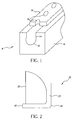
- the printhead 8 comprises a fluid delivery manifold 16 including a chamber often referred to as a liquid chamber or manifold bore 12 through which ink and other fluids pass to a nozzle plate 10.
- a fluid pathway often referred to as a slot 14 which is used to direct the fluid to the nozzle plate 10 from the manifold bore 12 is located between the nozzle plate 10 and the manifold bore 12.
- the nozzle plate or orifice plate 10 includes at least one nozzle bore 18 that is an orifice of defined cross section and length. Additional fluid pathways can be present between the orifice of the nozzle bore and the slot (such additional features not shown).
- Single or multiple nozzle bores are included in the nozzle plate or orifice plate.
- the term nozzle plate or orifice plate is familiar to those knowledgeable in the art of inkjet printing.
- a drop forming mechanism can be associated with the nozzle bore and/or the liquid chamber.
- the drop forming mechanism can be an electrical, mechanical, electromechanical, thermal, or fluidic mechanism, and is familiar to those knowledgeable in the art of inkjet printing.
- drop forming mechanisms can include single or multiple heating elements either near the nozzle bore or as an integral part of the nozzle bore.
- piezoelectric transducers can be located at or near the nozzle bore.
- the nozzle plate or orifice plate containing one or more nozzle bores can include electrical circuitry or complex microelectronic circuitry dedicated to various purposes such as producing drops or droplets and providing a means for electrical communication to the drop forming mechanism associated with at least one of the nozzle bores to provide a means for controlling the drop forming mechanism associated with at least one nozzle bore on the nozzle plate.
- the electrical circuitry can also perform other functions such as monitoring temperature or pressure.
- the nozzle plate or the manifold can include other assemblies for injecting energy into a jet of liquid or fluid emerging from the nozzle bore orifices on the nozzle plate for the purpose of producing drops.
- the printhead 8 can be incorporated into either a drop on demand printer or a continuous printer.
- ink and/or other fluids that pass through the nozzle plate and that are not printed on a substrate can be collected for reuse using printer devices or components familiar to those knowledgeable in the art of inkjet printing. These devices or components are called gutters and are dedicated to collecting unprinted drops or droplets so that the fluid can be reused.
- the gutter thus contains at least one surface for collecting fluid and a means for directing the collected drops and fluid to a fluid delivery system so that it can be reused.
- FIG. 2 shows a schematic for one design of a printer component known as a gutter 19.
- Unprinted fluid from an inkjet printhead is collected on a gutter collection surface 20 and flows through a fluid collection channel 22 formed in the space between the fluid collection channel wall 24 and the gutter collection surface 20 to a drain 26.
- unprinted fluid can be collected on the fluid collection channel wall 24 and then flow into fluid collection channel 22.
- the unprinted fluid, ink or otherwise, is then removed from the drain for recycling or discarding to waste.
- the drain is connected to a controlled vacuum, resulting in fluid removal from the fluid collection channel by suction, so that both gas and liquid can flow through the fluid collection channel.
- Continuous printers include other devices or printer components in the printing device are dedicated to controlling the trajectory of drops and droplets or deflecting drops or droplets using any means of trajectory control known in the art.
- Such inkjet printer components are known as drop deflectors or droplet deflectors.
- drop deflectors are positioned between an inkjet printhead that serves to produce the drops and a gutter that serves to collect fluid and ink for recycling or discarding to waste.
- Several means of controlling drop trajectory and introducing drop or droplet deflection by employing a drop deflector are known in the art and are familiar to those knowledgeable in the art of inkjet printing.
- the trajectory of drops can be controlled by means of deflection of charged drops in an electric field, deflection of drops through the action of an air flow at either elevated or reduced pressure, deflection of drops by means of unbalanced thermal stimulation of a jet of liquid, or any other means familiar to those skilled in the art of inkjet printing.
- Electrostatic deflection methods employ electrically conductive assemblies of wires, plates, or variously shaped conductive tunnels. These devices are called electrostatic deflection devices or electrostatic deflection inkjet printer components and include components such as charge plates and charge tunnels that are familiar to those knowledgeable in the art of inkjet printing.
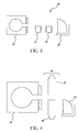
- FIG. 3 shows a schematic of an electrostatic deflection inkjet printer component.
- This inkjet printer component is also known as an electrostatic drop deflector 28.
- the electrostatic deflection inkjet printer component is located between the inkjet printhead 30 and the inkjet printer gutter 36.
- the electrostatic deflection inkjet printhead component is comprised of at least one charging electrode 32 and at least one deflection electrode 34. Such assemblies are familiar to those skilled in the art of continuous inkjet printing.
- drops or droplets are formed from a liquid jet emanating from a nozzle bore in the nozzle plate located on the manifold, and the drops are charged through the action of an electric field applied by the charging electrode 32.
- the charged drops can then be deflected by the deflection electrode 34 for the purpose of either directing the drops for collection on the collection surface of the gutter 36 or for the purpose of directing the drops to a substrate for the purpose of printing text or images through the selective imagewise deposition of drops or droplets on a substrate.
- the droplet deflector is configured to generate a gas flow interacting with the ink droplets, thereby separating ink droplets having one of a plurality of volumes from ink droplets having another of said plurality of volumes.
- the air drop deflector can also employ a pressure sensor positioned proximate to the output of the drop deflector component, where the pressure sensor is configured to generate a pressure indication signal.
- a controller coupled to said pressure sensor and configured to output a compensation signal based on the indication signal can be employed to provide an adjustment mechanism operatively coupled to said droplet deflector to adjust the gas flow generated by said droplet deflector in response to the compensation signal.
- Figure 4 shows a schematic of a drop deflector 40 using a gas flow.
- Drops are provided by the inkjet printhead 42 and fluid and inks that are to be recycled or discarded to waste are collected by the gutter 43.
- a gas flow is supplied by gas supply manifold 44 and collected by gas removal manifold 46 to provide a controlled gas flow between the gas supply manifold and gas removal manifold for the purpose of deflecting drops passing from the inkjet printhead towards the paper (or substrate) in the direction of the gutter.
- the gas removal manifold 46 can operate under reduced pressure so that, if desired, the gas supply manifold is not required for drop deflection.
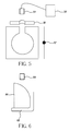
- FIG. 5 illustrates an inkjet printhead 52 with an electrode 54 positioned above the nozzle plate 56.
- the electrode 54 is used for the purpose of creating a micro-scale plasma proximate to the inkjet printer component, which in this example is the inkjet printhead.
- proximate refers to distances within 1 cm from the component.
- micro-scale plasma proximate to the inkjet printhead component can serve many purposes including ensuring initial cleanliness of the surfaces of the inkjet printer component, as well as surface modification of the surfaces of the inkjet printer component for the purpose of introducing improved hydrophobicity, hydrophilicity, or surface reactivity.
- the formation of micro-scale plasmas is of importance in the management of dried fluid deposits, such as those coming from inks, to improve the reliability of printing system startup and shutdown sequences and to improve the overall reliability of the printing system.
- a micro-scale plasma (also called micro-scale discharge) is generated by providing electrodes through which energy is coupled from an external supply to a region where the micro-scale plasma is generated.
- Micro-scale plasma refers to an electrical discharge in a gas where the discharge has at least one dimension less than 1 mm in extent, said extent being determined by the spatially localized luminous region, spatially localized ionized region, the region containing most of the active species of interest (for example, the full width at half the maximum concentration of a particular neutral active species such as atomic oxygen), or the spatial extent of the effect of the micro-scale plasma on the component being processed.
- micro-scale plasma region is spatially localized and it is recognized that it is potentially advantageous to translate one or more micro-scale plasmas to effect treatment of one or more additional regions and surfaces on the inkjet printer component of interest for the purpose of introducing improved hydrophobicity, hydrophilicity, or surface reactivity to larger surface areas on the inkjet printer component. It can also be beneficial to translate one or more micro-scale plasmas and optionally the associated electrode structures and power supplies to treat additional inkjet printer components as well.
- a contact through which energy is coupled to the plasma is herein referred to as an electrode.
- a second electrode used to provide reference to a first electrode or otherwise assist in coupling energy to the plasma is herein referred to as a counter electrode.
- Either the electrode or the counter electrode can be positively or negatively biased and therefore can serve as either an anode or a cathode in a diode discharge.
- Other types of electrodes include radio frequency antennas and microwave waveguides or applicators. In the case of radio frequency inductively coupled plasmas, conductive traces or wires forming an antenna serve as an electrode.
- the portions of a split ring conductive trace on either side of a discharge gap serve as electrode and counter electrode, while the split ring and a ground plane in combination serve as a waveguide.
- the electrode 54 can be connected to a power supply 58 and can be driven at an electrical potential with respect to a ground potential or other reference potential.
- the manifold of the inkjet printhead is held at ground potential.
- the electrical potential applied to the electrode can be DC or AC and the frequency of the AC potential can vary from Hz to GHz with amplitude from V to kV as limited by dielectric breakdown considerations.
- the electrode can be held at ground potential and the printer component itself can be driven at an electrical potential with respect to the ground potential of the electrode.
- a potential can be applied between an electrode and counter electrode with the inkjet printing component electrically isolated (“floating").
- Electrodes can be formed from conducting materials (e.g., metals, such as aluminum, tanatalum, silver, gold) or semiconducting materials (e.g., doped silicon, doped germanium, carbon, or transparent highly degenerate semiconductors, such as indium tin oxide, or aluminum-doped zinc oxide).
- conducting materials e.g., metals, such as aluminum, tanatalum, silver, gold
- semiconducting materials e.g., doped silicon, doped germanium, carbon, or transparent highly degenerate semiconductors, such as indium tin oxide, or aluminum-doped zinc oxide.
- conducting and doped semiconducting polymers, as well as conducting nanoparticulate dispersions can be useful in electrode construction.
- the electrodes can be passivated by dielectric coatings (for example, organic dielectrics such as epoxies or polyimide polymers, silicon oxide, silicon oxynitride, silicon nitride, tanatalum pentoxide, aluminum oxide), or they can be embedded in a dielectric material.
- dielectric coatings for example, organic dielectrics such as epoxies or polyimide polymers, silicon oxide, silicon oxynitride, silicon nitride, tanatalum pentoxide, aluminum oxide
- combination electrodes are permitted where a conducting material such as a metal or doped semiconductor is passivated or otherwise covered by or embedded in a semiconductor coating having different electrical characteristics where the semiconductor coating determines the electrical conductivity of the electrode.
- At least one electrode is located proximate to the component of interest.
- Proximate herein refers to distances within 1 cm from the component, including electrodes positioned within said proximate distance without contact to the component, brought into direct mechanical contact with the component, or formed directly on the component (integrated) by microfabrication, thin-film deposition, or lamination processes.
- the electrodes are integrated with the printer component.
- Integrated electrodes can be driven by external circuitry or incorporated into circuitry that is fabricated directly on the component, including active and passive circuit elements formed by techniques known in the art of microelectronics and microelectromechanical systems (MEMS) manufacturing.
- MEMS microelectronics and microelectromechanical systems
- Proximate electrodes can be driven by either external circuitry or by circuitry that is fabricated directly on the component, including active and passive circuit elements formed by techniques known in the art of microelectronics and microelectromechanical systems (MEMS) manufacturing.
- one or more microplasmas can be generated by using both odd and even numbers of electrodes depending on the specific application.
- the electrodes can be single electrodes or an array of electrodes with a single counter electrode or counter electrode array.
- electrodes and electrode arrays can be shaped to optimize the micro-scale plasma generation and treatment effect for a specific component to be treated.
- the electrode 54 can have various geometries and can be a wire that is either straight or, shaped, for example, as a loop or coil or some other 2- or 3- dimensional shape.
- the electrode surface presented to the volume where the micro-scale plasma is formed can have the characteristics of the tip of a wire or it can have the characteristics of an asperity from a three dimensional geometrical construct such as the tip of a pyramid, a surface with roughness features on the micro-scale, or some other 3-dimensional topography.
- the term electrode is also applied to a more complex assembly where a portion of the assembly is electrically conductive and an additional portion of the assembly is nonconductive, such as the case of an insulating rod covered with an electrically conductive coating.
- the electrode can have hollow portions such as would be found in an insulating tube wound with wire or otherwise coated with a conductive material such as a metal.
- micro-scale plasma treatment process is intended to run under ambient conditions, it can be advantageous to control the plasma treatment environment by establishing a gas flow of specific gases.
- the composition of flowing gases can be selected depending on the desired purpose of the micro-scale plasma.
- compounds that can be activated to produce condensable species can be provided in the gas admitted to the plasma region in order to effect plasma enhanced chemical vapor deposition of a coating onto the component being treated.
- a suitable fluorine- and carbon-bearing gas can be selected in combination with a suitable carrier gas, capable of conveying the micro-scale-plasma-activated species to the appropriate location for deposition on the inkjet printer component.
- condensable materials well known in the plasma deposition and plasma enhanced chemical vapor deposition art can be similarly produced.
- silanes, siloxanes, and other gases can be admitted to produce silicon oxide, silicon nitride, or silicone films.
- Other heteroatomic reactants such as ammonia can be added to the gas admitted to the plasma region in order to produce specific activated species, or gases from the ambient air can be entrained in plasma region to produce reactive species.
- gases known to produce volatile species upon plasma activation and contact with the deposit can be introduced proximate to the micro-scale plasma.
- a suitable carrier gas is one that does not react substantially with the intended micro-scale-plasma-activated species over length scales and time scales such that useful amounts of said species are transported to the desired location.
- Some common carrier gases are inert or noble gases, such as helium, neon, and argon.
- molecular gases such as nitrogen (N 2 ) can be useful carrier gases, depending on the desired purpose of the micro-scale plasma.
- noble gases such as helium
- Heavier noble gases such as krypton and particularly xenon can be added to the gas composition to alter the emission spectrum radiating from the micro-scale plasma region.
- xenon gas to the micro-scale plasma region is particularly useful in achieving enhanced ultraviolet emission from the micro-plasma during operation for such processes as elimination of biofouling debris (debris as a result of surface contamination from microorganisms) as well enhancing oxidative surface processes utilizing ozone or other oxidizing reactive neutral species produced by the micro-scale plasma.
- the selection of the composition of the plasma treatment gas is based on the intended effect on the component, and the micro-scale plasma process can be tailored to clean, activate, or passivate the inkjet printer component surface as desired, and the gas composition can further be tailored to improve the operation and stability of the micro-scale plasma, as well as the efficiency of the micro-scale plasma process.
- near atmospheric pressure includes pressures between 400 and 1100 Torr, and preferably pressures between 560 and 960 Torr.
- Process pressures in the higher portion of this range can be achieved by pressurizing a manifold dedicated to providing the treatment gas in the vicinity of the component to be treated or a manifold that might otherwise be used for providing air flow or ink flow in the normal printing process.
- the manifold can be drawn to a reduced pressure in order to draw treatment gas (provided by ambient air or an external gas supply) into the plasma treatment region.
- gas flow in the regions around the electrode and inkjet printer component there can be gas flow in the regions around the electrode and inkjet printer component.
- gas at ambient pressure can flow around the electrode from all sides to surround the electrode and the printer component.
- the inside of the printer component in this case the manifold bore of the inkjet printhead, can be held under reduced pressure to force gas to be drawn through the nozzle bore into the inkjet printhead.
- the inside of the printer component can be held under elevated pressure to force gas through the nozzle bore into the space between the printer component and the electrode.
- the management of gas flow is for the purpose of maintaining the desired composition and flow of gas proximate to the micro-scale discharge, which is formed proximate to the electrode. It is also recognized that the management of gas flow proximate to the micro-scale plasma (near, around, and through the micro-scale plasma) provides a means to direct reactive species formed by the micro-scale plasma in the gas phase towards an intended location.
- Figure 6 illustrates an inkjet printer gutter similar to that shown in Figure 2 with an electrode 64 positioned above the gutter collection surface 66 or fluid collection surface 66.
- the electrode 64 is used for the purpose of creating a micro-scale plasma proximate to the inkjet printer component, which in this example is the gutter, proximate herein referring to distances within 1 cm from the component.
- the formation of a micro-scale plasma proximate to the inkjet printer component can serve many purposes including ensuring initial cleanliness of the surfaces of the inkjet printer component, as well as modification of the surfaces of the inkjet printer component for the purpose of introducing improved hydrophobicity, hydrophilicity, or surface reactivity, and maintaining the surface cleanliness or surface properties during printer use.
- fluorohydrocarbon oxides of silicon, carbides of silicon, or nitrides of silicon can be deposited on the fluid collection surface to modify its wetting properties.
- the formation of micro-scale plasmas is of importance in the management of dried fluid deposits, such as those coming from inks, which can interfere with the function of the fluid collection surface and the overall operation of the gutter component.
- micro-scale plasmas to clean and modify surfaces of portions of the gutter component thus enables control of critical surface conditions and thereby improves the reliability of printing system startup and shutdown sequences as well as overall operational reliability.
- elements of the inkjet printer gutter for example, the inkjet printer gutter collection surface or the inkjet printer gutter fluid collection channel wall can be employed as electrodes in some configurations.
- the fluid collection channel 68 in the gutter assembly can be used as a means to provide flowing gas to the region proximate to the micro-scale plasma in order to provide the desired stability and chemical or physical effect of the micro-scale plasma.
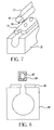
- FIG. 7 shows an alternate configuration of a single electrode 76 positioned over an inkjet printer component.
- the inkjet printer component is an inkjet printhead comprised of a nozzle plate 74 and an attached manifold 72.
- the single electrode in this case is a three-dimensional split cylinder resonator electrode attached to a planar connector 77.
- the split cylinder electrode can be constructed so that the outermost layer is conductive.
- the interior of the electrode can be hollow or filled with a solid dielectric and further include a grounded concentric cylinder that serves as a ground plane and that is connected to a ground plane embedded in the planar connector 77.
- the planar connector can have a hollow or dielectric-filled volume between its outer conducting surfaces and the embedded ground plane.
- the ground plane can be comprised of a concentric conductive cylinder external to the split cylinder electrode in combination with planar conductors external to the planar connector.
- the connector 77 need not be planar, and the cylinder 76 need not have a circular cross section.
- the interior of the split cylinder resonator electrode is hollow then the interior portion of the electrode can also be used to deliver a flow of gas to the gap in the split cylinder electrode to produce micro-scale plasmas at atmospheric pressure in controlled atmospheres.
- the advantage of the split cylinder resonator electrode is the ability to create a micro-plasma that is elongated in one dimension, thereby allowing the treatment of multiple regions on the inkjet printer component simultaneously.
- the split cylinder resonator electrode has an operating frequency determined by the dimensions of the cylinder and can vary from kHz to GHz.
- Figure 8 shows a single electrode 82 covered with a coating 84 and positioned above an inkjet printer component.
- the inkjet printer component in this example is an inkjet printhead comprised of a nozzle plate 86 and an attached manifold 88.
- the coating on the electrode can have any thickness with a preferred thickness ranging from 10 nm to 10 microns.
- the coating material can be metallic, semiconducting, or insulating.
- the coating can be comprised of a corrosion resistant metal such as tantalum or platinum.
- the coating can be comprised of a semiconducting material like silicon carbide or a conducting oxide.
- the coating can also be comprised of a dielectric material like Teflon, vitreous silicon dioxide, silicon oxide, aluminum oxide or the like.
- the coating can be a combination of materials or a composite material wherein the term composite denotes a material having two or more (a plurality of) regions with chemically distinct compositions.
- the coating serves one or more purposes including chemically passivating the underlying electrode material towards highly reactive species formed in the micro-scale plasma as well as influencing the secondary emission characteristics of the electrode (e.g., the coefficient for secondary electron emission by ion impact).
- the electrode can be either at ground potential or at a potential different from ground potential and can be driven using either DC voltages or AC voltages having amplitudes from 1 volt to 50 kV, as described previously in the description of Figure 5 . When AC voltages are employed, the frequency can be from 1 Hz to 100 GHz with a preferred frequency range from 10 kHz to 10 GHz.
- Figure 9 illustrates a plurality of electrodes 92, 94 positioned above the nozzle plate 96, nozzle bore 99, and manifold 98 of an inkjet printhead component.
- the electrodes can be as described in Figure 5 with the difference that there is more than one electrode present and positioned above the inkjet printer component.
- the electrodes 92, 94 can be electrically driven by the application of a potential.
- a variety of configurations for applying electrical potentials to a plurality of electrodes are possible. The purpose of applying various electrical potentials to the electrodes is to produce one or more micro-scale plasmas proximate to the inkjet printer component.
- the electrical potential applied to the electrodes can be DC or AC and the frequency of the AC potential can vary from 1 Hz to 100 GHz with amplitude from 1V to 50kV as limited by dielectric breakdown considerations.
- the inkjet printer component can be either held at a reference potential or at ground potential or remain electrically floating.
- electrode 92 can be electrically driven and electrode 94 can be held at a reference potential or at a ground potential.
- the micro-scale plasma is produced between electrodes 92, 94 or between each electrode 92, 94 and the nozzle plate 96.
- electrical potential can be applied between electrodes 92 and 94 to produce a micro-scale plasma in the gap or region between the two electrodes.
- Species produced in the micro-scale plasma then travel to the proximate regions of the inkjet printer component to effect the intended surface treatment. Pairs of such electrodes can be positioned in correspondence with features in the inkjet printer component (e.g., nozzle bores in a nozzle plate) to produce a plurality of localized micro-scale plasmas for addressing a plurality of features.
- the application of a suitable reference potential to the inkjet printer component can extend the region of the micro-scale plasma towards the inkjet printer component while still retaining the dimensional scale of the micro-scale plasma to 1mm or less between electrodes 92, 94.
- Extending the micro-scale plasma region in one or two dimensions is useful to enhance the efficacy of the atmospheric pressure micro-scale plasma processing for the purpose of, for example, cleaning, surface deposition, or enhancing surface reactivity.
- a plurality of electrodes 92, 94 can be arranged so that each one is positioned in correspondence with a feature in the inkjet printer component.
- the plurality of electrodes can be driven together (in parallel) or independently relative to the inkjet printer component to produce localized micro-scale plasmas at each electrode, and electrically conducting portions of the inkjet printer component function as counter electrodes.
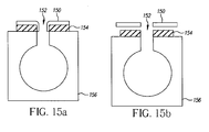
- Figure 10a shows an example of a plurality of single electrodes (or multiple single electrodes) 102, 104 where each single electrode is embedded in a dielectric material 101 and positioned over an inkjet printer component.
- Figure 10b shows a plurality of electrodes 108 embedded in the same single dielectric material 101 positioned above an inkjet printer component.
- the inkjet printer component is an inkjet printhead with a nozzle plate 106.
- embedded means that the electrode is substantially surrounded by solid or liquid material on all its outer surfaces.
- the purpose of embedding electrodes is to protect the electrodes from potentially corrosive micro-scale plasma generated species that could lead to the destruction of the electrode.
- the dielectric material 101 in which the electrodes are embedded has an electrical resistivity greater than 10 5 ohm-cm and the thickness of the dielectric material can be any thickness as is appropriate for the micro-scale plasma application and is determined by the operating voltage and dielectric breakdown characteristics of the dielectric material as well as method of electrode manufacture.
- the dielectric material 101 can be selected from any number of materials with electrical resistivity greater than 10 5 ohm-cm including: Teflon, epoxies, silicone resins, polyimides, or other low-reactivity thermally stable organic polymers; or carbon containing composite materials where the term composite material refers to a solid containing at least two regions of differing chemical composition.
- composite materials are, for example, fiberglass impregnated epoxy or glass fiber reinforced and glass filled Teflon polymer. It will be appreciated that other composite materials are possible and are envisioned to be within the scope of this invention.
- dielectric materials are: inorganic insulating materials like magnesium oxide and derivative magnesium containing oxides, boron oxide and derivative boron containing oxides, silicon oxide and derivative silicon containing oxides, aluminum oxide and derivative aluminum containing oxides, titanium oxide and derivative titantium containing oxides, tantalum oxide and derivative tantalum containing oxides, niobium oxide and derivative niobium containing oxides, hafnium oxide and derivative hafnium containing oxides, chromium and derivative chromium containing oxides, zirconium oxide and derivative zirconium containing oxides, (insulating binary metal oxides) as well as nitrides, oxynitrides, sulfides and more complex ternary and higher order oxides, nitrides, oxynitrides, and sulfides.
- inorganic insulating materials like magnesium oxide and derivative magnesium containing oxides, boron oxide and derivative boron containing oxides, silicon oxide and derivative silicon containing oxides, aluminum
- derivative metal containing oxides means oxide based dielectric compounds containing at least 20 atomic percent of the specified metal.
- the compound zirconium oxide containing 20 percent cerium oxide is a derivative zirconium oxide. It is also a derivative oxide of cerium.
- the dielectric material can be crystalline, vitreous, or amorphous. It will be appreciated that other dielectric materials are possible and will be familiar to those skilled in the art of dielectric materials and are envisioned within the scope of the present invention.
- the dielectric coating can also be textured with asperities or it can be smooth and asperity free. Various types of textured dielectric coatings are possible and are envisioned within the scope of the present invention.
- the electrodes can be electrically driven in a variety of configurations for the purpose of producing a micro-scale plasma proximate to the inkjet printer component.
- Figure 11 shows an example of an elongated electrode 110 positioned over and proximate to the nozzle plate 112, nozzle bore 114, and manifold 116 of an inkjet printhead component.
- the electrode 110 is shown as rectangular in Figure 11 , other electrode shapes within the scope of this invention are envisioned where the aspect ratio of the elongated dimension of the electrode (substantially lying in the plane parallel to at least one surface of the inkjet printhead component) to at least one of the other two dimensions is greater than 10.
- the electrode could have the shape of an elongated trigonal prism or some other geometrical construct.
- the electrode can simply be a length of wire where the diameter of the wire is at least 10 times smaller than the length of the wire lying in the plane parallel to at least one surface of the inkjet printer component.
- the electrode shown in Figure 11 can be electrically driven as discussed in Figure 5 for the purpose of forming a micro-scale plasma region proximate to the inkjet printer component.
- the use of flowing gas around the electrode 110, as described in the discussion of Figure 5 including the use of the inkjet printer component itself for the purpose of flowing gas proximate to the inkjet printer component and micro-scale plasma region is also contemplated here.
- Figure 12 illustrates an elongated electrode 120, as described in Figure 11 , that is coated with a material 122, as described in Figure 8 , or embedded in a dielectric layer 122, as described in Figure 10 , wherein said elongated electrode is positioned proximate to the nozzle plate 124, nozzle bore 126 and manifold 128 of an inkjet printer component.
- a coated or embedded elongated electrode are envisioned within the scope of the present invention.
- configurations involving a plurality of elongated electrodes are envisioned within the scope of the present invention, including a pair or a plurality of pairs of electrodes driven with respect to one another to form a micro-scale plasma in the gap between the elongated electrodes in each pair and proximate to the inkjet printer component.
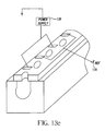
- Figures 13a, 13b , and 13c illustrate various configurations of electrodes and counter electrodes that are integrated into an inkjet printer component known as an inkjet printhead.
- the term integrated as employed here means to arrange and fabricate constituent parts to form an inseparable whole.
- a plurality of electrodes 130 are integrated with the inkjet printhead nozzle plate 132 proximate to the nozzle bore 134 and manifold 136.
- Integrated electrodes 130 can be passivated or embedded with dielectric material as discussed in Figures 8 , 10 , and 12 .
- FIGS 13a, 13b , and 13c Examples of electrical driving circuitry 138 for the purpose of producing micro-scale plasmas proximate to the inkjet printer component are also shown in Figures 13a, 13b , and 13c and it is recognized that other configurations of electrodes and driving circuits are possible and envisioned within the scope of this invention.
- Figure 13a and 13b illustrate various views of a plurality of electrodes integrated on a nozzle plate and electrically driven through external circuitry, for example a power supply. It is recognized that with the advent of miniaturization of high power devices that the entire power supply can be integrated onto the inkjet printhead component as well, and this is envisioned within the scope of this invention.
- the electrodes can be driven in a variety of configurations as described in Figures 5 , 7 , and 9 and it is recognized that other electrical configurations are possible and fall within the scope of this invention.
- an electrode and a counter electrode are driven against each other using electrical circuitry.
- Figure 13b illustrates a plurality of electrodes driven relative to an external reference.
- the electrodes can be RF antennae or microwave waveguides similar to those described in US Patent No. 5,942,855 and US Patent Application Publication No. 2004/0164682 A1 by Hopwood et al. where the gap of the microwave guide electrode or the region of localized RF energy from the RF antennae electrode is located proximate to the nozzle bore 134.
- the electrodes can be electrically driven relative to a counter electrode, which in Figure 13b can be another part of the inkjet printer component such as the manifold 136, or it can be an external counter electrode, which is not shown in Figure 13b .
- Figure 13c illustrates a plurality of electrodes and counter electrodes integrated into an inkjet printer component called an inkjet printhead.
- the total number of the integrated electrodes can be odd or even.
- Figure 13c also shows a configuration for driving said integrated electrodes where every other electrode is connected to a terminal 139 held at a reference potential, V ref.., relative to the neighboring driven electrodes.
- V ref is a reference potential which can be a non-zero DC potential or can be grounded by connecting the terminal to ground potential.
- the potential at the electrodes attached to terminal 139 can be manipulated through modulation of V ref using methods known to those knowledgeable in the art of plasma generation and consistent with the integrated electrode configuration (for example, number and relative sizes of electrodes and counter electrodes, presence or absence of dielectric material, etc.).
- Figure 14 shows a plurality of elongated electrodes 140 integrated into the inkjet printer component.
- a plurality of elongated electrodes 140 as described in Figure 11 or Figure 12 is integrated onto the nozzle plate 142 proximate to nozzle bores 144 and manifold 146 and are electrically driven with electrical circuitry 148. It is appreciated that, as discussed in Figure 11 and 12 , there are a variety of means possible for driving the elongated electrodes for the purpose of producing at least one micro-scale plasma proximate to the inkjet printer component.
- the electrical circuitry for controlling, producing, and maintaining a micro-scale plasma with a plurality of integrated elongated electrodes is optionally integrated into the inkjet printhead component.
- Figure 15a and 15b show both integrated and non-integrated electrical shielding 150 proximate to a nozzle bore 152 on a nozzle plate 154 and manifold 156 of an inkjet printhead inkjet printer component.
- Electrical shielding is comprised of an electrically conducting layer that is interposed between a source of electrical noise, such as a micro-scale plasma, and the inkjet printer component where said electrical shield is present for the purpose of improving operational reliability of the inkjet printer component.
- the electrical shielding can be fabricated out of any electrically conducting material with a resistivity less than 100 ohm-cm.
- Typical electrical shielding is fabricated out of metals such as copper, aluminum and aluminum alloys, steel, tantalum and tantalum alloys, gold and gold alloys, silver and silver alloys, niobium and niobium alloys, and titanium and titanium alloys.
- Transparent conducting materials such as transparent conducting oxides, can also be used to fabricate electrical shielding.
- conductive polymers for example, polythiophene-based materials
- conductive dispersions of carbon-based materials for example carbon nanotubes
- Nanoparticulate dispersions of conductive materials can also be employed to fabricate electrical shielding.
- the electrical shielding can be optionally integrated with the inkjet printer component to improve the inkjet printer component operational reliability.
- the production of micro-scale plasma can require voltages which exceed the normal operating voltages of the inkjet printer component, or it can produce localized currents that exceed normal operating currents, and an additional purpose of the optionally integrated electrical shielding is to protect the inkjet printer component from damage that could occur if the inkjet printer component was exposed to voltages or currents in excess of the normal operating conditions or in excess of damage thresholds.
- the inkjet printer component By interposing the electrical shield between the source of electrical noise, such as a micro-scale plasma, and substantially all potentially sensitive electrical circuitry, including CMOS circuits and other electrical and microelectronic circuitry known to those familiar with the electrical design of inkjet printer components, the inkjet printer component is effectively protected from the source of electrical noise.
- the source of electrical noise such as a micro-scale plasma
- substantially all potentially sensitive electrical circuitry including CMOS circuits and other electrical and microelectronic circuitry known to those familiar with the electrical design of inkjet printer components
- the electrical shielding 150 can be connected by any method known to produce electrical continuity with a resistance of less than 10 ohms to a reference potential or a ground potential. Alternatively, there are situations in which it is desirable to allow the electrical shielding to remain unconnected to any reference potential source so that the electrical shield acquires the potential associated with the said source of electrical noise. This configuration is known in the art as electrically floating. For example, if sensitive circuitry can remain electrically floating instead of being grounded, then the circuitry will attain the floating potential, the potential at which a floating contact draws no net charge from the plasma, when exposed to a plasma.
- the shield should be allowed to float electrically with the circuitry upon exposure to the source of electrical noise such as a micro-scale plasma.
- the potential difference between plasma and the article can be significantly reduced relative to the case of a grounded article, and thus, the energies of ions impinging on the article can be significantly reduced.
- the plasma potential can rise substantially (hundreds of volts) during one half cycle of the applied voltage.
- micro-scale plasmas It can be desirable in some applications of micro-scale plasmas to allow the electrical shield interposed between the micro-scale plasma and the inkjet printer component to float and optionally to allow the inkjet printer component itself to float because the floating shield absorbs the ion energy impinging on the surfaces proximate to the micro-scale plasma.
- This ion energy not only comes in the form of translational kinetic energy but also comes in the form of the energy associated with the ionization potential of the ionized species, said energy from the ionization potential being imparted to the surface with which the ion collides.
- electrical shielding is intended to improve operational reliability of the inkjet printer component
- the electrical shielding can perform the additional function of a counter electrode in addition to the primary function of protecting sensitive components on the inkjet printer component for the purpose of improving operational reliability.
- Figure 16 shows an example of a dielectric layer 160 interposed between a plurality of electrodes 162 and electrical shielding 164 where the electrodes 162, dielectric layer 160 and electrical shielding 164 are integrated onto a nozzle plate 166 proximate to at least one nozzle bore 168 and manifold 169 on an inkjet printhead inkjet printer component.
- the purpose of the integrated dielectric layer is to electrically insulate the plurality of electrodes from the electrical shielding so that the electrodes do not electrically conduct to the electrical shielding during application of voltage for the purpose of producing a micro-scale plasma proximate to the inkjet printer component.
- Suitable types of electrical shielding include conductive metals such as gold, copper, aluminium, tantalum, etc., as well as highly doped semiconductor materials such as silicon or polysilicon, doped with phosphorus or boron, doped or otherwise conductive forms of silicon carbide, and doped or otherwise conductive forms of diamond like carbon.
- Conductive oxide materials such as indium tin oxide, fluorine-doped tin oxide, and aluminum-doped zinc oxide can also be used.
- the electrical shielding can be either connected to a ground potential or a reference potential: alternatively, the electrical shielding can remain unconnected to any reference potential and be allowed to acquire the potential induced by the surrounding electrical noise source or allowed to float electrically.
- the electrodes can be electrically driven for the purpose of producing a micro-scale plasma using any means known in the art of plasma generation and that there are a variety of configurations for electrically driving a plurality of electrodes that can be contemplated and are envisioned to be within the scope of this invention.
- the plurality of electrodes integrated onto the inkjet printer component can be of a variety of sizes and shapes.
- the plurality of electrodes integrated onto the inkjet printer component can be coated with a variety of materials as discussed previously or uncoated, embedded or unembedded, elongated or otherwise extended in at least one dimension. It is also understood that gas flow can be applied to the integrated electrode assembly shown in Figure 16 as previously mentioned in the discussion of Figure 5 .
- the manifold 169 can be held at either elevated or reduced pressure relative to ambient for the purpose of influencing gas flow proximate to the micro-scale plasma that is produced proximate to the integrated electrodes 162 on the dielectric layer 160 of Figure 16 .
- Figure 17 shows another example of a plurality of elongated electrodes 170 integrated on the surface of nozzle plate 172, proximate to at least one nozzle bore 174.
- the nozzle plate 172 is affixed to manifold 176.
- a dielectric layer 178 and electrical shielding 179 are interposed between the plurality of elongated electrodes 170 and the nozzle plate 172.
- interdigitated electrodes and counter electrodes are integrated in an inkjet printer component.
- the integrated interdigitated electrodes can be optionally positioned so that the nozzle bore 174 of the nozzle plate 172 is located in the space between at least two of the integrated elongated electrodes.
- Figure 17 also shows an example of a configuration for driving the integrated interdigitated electrodes for the purpose of producing a micro-scale plasma proximate to the inkjet printer component. It is recognized that a variety of electric circuits can be used to drive electrodes, including various electrical configurations of the electrical shielding, as has been previously discussed.
- Figure 18a shows a composite electrode comprising alternating conductive 180 and dielectric 182 layers along a direction in a plane parallel to a surface of an inkjet printer component 184.
- the inkjet printer component is an inkjet printer gutter.
- the electrically conductive layers comprise a plurality of electrodes and counter electrodes and are electrically driven so that every other electrically conductive layer (alternating conductive layers) is electrically driven in parallel fashion by a power supply 185, and the remaining counter electrodes are grounded or otherwise connected to the other side of said power supply.
- the power supply can be DC or AC.
- the spacing of the electrically conductive layers comprising a plurality of electrodes and counter electrodes may correspond to dimensions of importance to printer design, such as the spacing between nozzles on an inkjet printer component.
- electrode pairs 186 are chosen as adjacent conducting layers from the alternating layers of conductive and dielectric layers, where dielectric layers are interposed between each conductive layer, and each specified electrode - counter electrode pair chosen from adjacent conductive layers is independently electrically driven by separate power supplies 188, which can be DC or AC. It is recognized that such a configuration can operate over a wide range of frequencies and that the plurality of power supplies can operate over a plurality of frequencies for the purpose of generating adjacent regions of micro-scale plasma having different characteristics according to the frequency of operation of the chosen electrode- counter electrode pair. Additionally, the dielectric layers need not be continuous and can be spacers instead of solid material, and that a substantial portion of the volume separating conductive layers can be hollow.
- FIGS 19a through 19e show various example geometries for electrodes used to generate micro-scale plasmas. However, other electrode geometries contemplated for the purpose of producing micro-scale plasma can be integrated appropriately into an inkjet printer component as described in the discussion of Figures 13 through 17 .
- Figure 19a shows a split ring 190 and connector or transmission line 191.
- Figure 19b shows a patterned electrode 193 with a comb-like structure wherein the protrusions define a gap 197 relative to a counter electrode 195.
- the gap 197 is aligned over an array of nozzle bores 198 on an inkjet printer component (not shown).
- Figure 19c shows an electrode 193 and counter electrode 195 each having a pointed feature, said pointed features defining a gap 197 between the two electrodes wherein optionally lies at least one nozzle bore 198.
- Figure 19d shows an electrode 193 and counter electrode 195 each having a plurality of asperities located along the length of the edge of the electrode so as to define a gap 197 having a plurality of regions that are narrower and have more concentrated electric field when a potential is applied across the electrode-counter electrode pair.
- one or more nozzle bores 198 optionally are located within the gap region 197.
- Figure 19e shows an electrode having a plurality of asperities located around the perimeter of a feature, for example a nozzle bore 198 on an inkjet printer component.
- the electrodes and counter electrodes of Figures 19a through 19e can be produced by thin-film deposition and patterning techniques known in the art of microelectronics, microfabrication, and microelectromechanical systems manufacture. Furthermore, they can be stamped from a thin sheet stock or patterned from metal sheets using any technique familiar to those skilled in the art of microfabrication such as electrical discharge machining or chemical etching methods that employ photoresist and etchant solutions.
- the electrodes can be fabricated in sheet form and, in particular, structures such as those shown in Fig. 19a, Fig. 19c, and Fig 19d can be assembled with a dielectric material between the electrodes (or otherwise electrically separated to prevent conduction between said electrodes) to produce a structure or structures as shown in Fig. 18 , wherein the gaps between electrode and counter electrode define a region for forming a micro-scale plasma.
- the multiple gaps between the electrode and counter electrode can be positioned proximate to an inkjet printer component and when driven with suitable electrical excitation can produce an array of micro-scale plasmas in substantially one direction and along a direction lying in a plane substantially parallel to at least one surface of an inkjet printing component.
- An assembly of comb electrodes like those of Fig. 19b can be similarly stacked and interleaved with dielectric layers to produce a composite electrode that would produce a plurality of micro-scale plasmas in a two-dimensional array, which could be used to address a plurality of features on an inkjet printer component.
- the electrode configuration might incorporate additional conductive structures. For example, ground planes separated from electrodes by dielectric layers or air gaps can be necessary in order to guide microwaves to the gaps where the micro-scale plasma is generated.
- Electrodes and counter electrodes integrated or otherwise, for the purpose of producing micro-scale plasma proximate to an inkjet printer component are permitted.
- the choice of a particular electrode geometry is made in accordance with the geometry of the inkjet printer component and its associated features.
- micro-scale atmospheric pressure plasmas there are a variety of means to produce micro-scale atmospheric pressure plasmas.
- a variety of means to couple power to the discharge a variety of electrode configurations, and a variety of treatment gas.
- the combination of power supply, impedance matching device, electrode and component configuration, and treatment gas should produce a micro-scale atmospheric pressure plasma in the normal or abnormal glow regime that is sufficiently stable that it does not become an arc.
- the glow-discharge plasma regime is characterized by distinct regions of uniform glow-like appearance, operating voltages below the break-down voltage, and having negligible slope (normal glow) or positive slope (abnormal glow) to the voltage-current characteristic (see for example Electrical Discharges in Gases, F.M. Penning, Gordon and Breach, New York, 1965, p. 41 ).
- the glow discharge regime has lower operating voltage and higher current density (therefore, higher plasma density) than the Townsend regime and is more stable and exhibits less electrical noise and associated interference than the arc regime, which is characterized by considerably higher current density and lower operating voltage.
Claims (9)
- Verfahren zum Behandeln eines Bauteils eines Tintenstrahldruckers, umfassend:Bereitstellen einer Elektrode (64, 76, 82, 92, 94, 110, 120, 130), die in das zu behandelnde Bauteil des Tintenstrahldruckers integriert ist;Bereitstellen einer Gegenelektrode, die in der Nähe des zu behandelnden Bauteils des Tintenstrahldruckers angeordnet und von der Elektrode beabstandet ist, um Kontakt zu vermeiden;Einführen eines Plasmabehandlungsgases in einen Bereich, der in der Nähe des zu behandelnden Bauteils des Tintenstahldruckers liegt; undBehandeln des zu behandelnden Druckerbauteils durch Anlegen von Spannung an die Elektrode, wodurch ein Plasma mit Mikroabmessungen nahezu bei Luftdruck erzeugt wird, wobei das Plasma mit Mikroabmessungen auf das zu behandelnde Bauteil des Tintenstrahldruckers einwirkt, und wobei das Anlegen von Spannung an die Elektrode das Anlegen von Spannung zwischen Elektrode und Gegenelektrode umfasst.
- Verfahren nach Anspruch 1, weiterhin umfassend:Hin- und Herbewegen des zu behandelnden Druckerbauteils.
- Verfahren nach Anspruch 1, weiterhin umfassend:Kontrollieren der Luftdruckbedingungen im Bereich, der in der Nähe des zu behandelnden Druckerbauteils liegt.
- Verfahren nach Anspruch 1, wobei das Druckerbauteil einen elektrischen Schaltkreis aufweist und das Verfahren zudem umfasst:elektrisches Abschirmen des elektrischen Schaltkreises gegenüber der Spannung, welche während der Behandlung des Druckerbauteils angelegt wird.
- Verfahren nach Anspruch 1, worin das zu behandelnde Druckerbauteil mindestens aus einer Flüssigkeitskammer, einer Düsenplatte, einer Rinne oder einem Düsenloch besteht.
- Verfahren nach Anspruch 1, worin die Gegenelektrode Teil des zu behandelnden Druckerbauteils ist.
- Verfahren nach Anspruch 1, weiterhin umfassend:Bereitstellen zusätzlicher Elektroden, die in der Nähe des zu behandelnden Druckerbauteils angeordnet sind; undBereitstellen zusätzlicher Gegenelektroden, die in der Nähe des zu behandelnden Druckerbauteils angeordnet sind.
- Verfahren nach Anspruch 1, weiterhin umfassend:Bereitstellen zusätzlicher Elektroden, die in der Nähe des zu behandelnden Druckerbauteils angeordnet sind.
- Verfahren nach Anspruch 1, worin die Elektrode entweder einen Mikrowellenleiter oder eine Hochfrequenz-Antenne umfasst.
Priority Applications (1)
| Application Number | Priority Date | Filing Date | Title |
|---|---|---|---|
| EP10159905A EP2208617A1 (de) | 2007-10-17 | 2008-10-08 | Plasmabehandlung von Druckerkomponenten bei Umgebungsbedingungen |
Applications Claiming Priority (2)
| Application Number | Priority Date | Filing Date | Title |
|---|---|---|---|
| US11/873,655 US8029105B2 (en) | 2007-10-17 | 2007-10-17 | Ambient plasma treatment of printer components |
| PCT/US2008/011595 WO2009051654A2 (en) | 2007-10-17 | 2008-10-08 | Ambient plasma treament of printer components |
Related Child Applications (1)
| Application Number | Title | Priority Date | Filing Date |
|---|---|---|---|
| EP10159905.8 Division-Into | 2010-04-14 |
Publications (2)
| Publication Number | Publication Date |
|---|---|
| EP2200829A2 EP2200829A2 (de) | 2010-06-30 |
| EP2200829B1 true EP2200829B1 (de) | 2013-02-13 |
Family
ID=40224129
Family Applications (2)
| Application Number | Title | Priority Date | Filing Date |
|---|---|---|---|
| EP08839367A Not-in-force EP2200829B1 (de) | 2007-10-17 | 2008-10-08 | Plasmabehandlung von druckerbestandteilen unter raumbedingungen |
| EP10159905A Withdrawn EP2208617A1 (de) | 2007-10-17 | 2008-10-08 | Plasmabehandlung von Druckerkomponenten bei Umgebungsbedingungen |
Family Applications After (1)
| Application Number | Title | Priority Date | Filing Date |
|---|---|---|---|
| EP10159905A Withdrawn EP2208617A1 (de) | 2007-10-17 | 2008-10-08 | Plasmabehandlung von Druckerkomponenten bei Umgebungsbedingungen |
Country Status (6)
| Country | Link |
|---|---|
| US (1) | US8029105B2 (de) |
| EP (2) | EP2200829B1 (de) |
| JP (1) | JP2011500369A (de) |
| CN (1) | CN101808827B (de) |
| TW (1) | TW200927504A (de) |
| WO (1) | WO2009051654A2 (de) |
Families Citing this family (19)
| Publication number | Priority date | Publication date | Assignee | Title |
|---|---|---|---|---|
| US8609203B2 (en) * | 2008-06-06 | 2013-12-17 | Fujifilm Manufacturing Europe B.V. | Method and apparatus for plasma surface treatment of moving substrate |
| GB0903299D0 (en) | 2009-02-26 | 2009-04-08 | Guys And St Thomas Nhs Foundat | Composition and methods |
| JP2013519991A (ja) * | 2010-02-17 | 2013-05-30 | ヴィジョン ダイナミックス ホールディング ベー.フェー. | 基板の表面をパターニングするためのプラズマ放電を発生させる装置および方法 |
| US20130116682A1 (en) * | 2011-11-09 | 2013-05-09 | Colorado State University Research Foundation | Non-Stick Conductive Coating for Biomedical Applications |
| US20150162523A1 (en) * | 2013-12-06 | 2015-06-11 | Murata Manufacturing Co., Ltd. | Piezoelectric device |
| WO2015126431A1 (en) * | 2014-02-24 | 2015-08-27 | Empire Technology Development Llc | Increased interlayer adhesions of three-dimensional printed articles |
| TWI569690B (zh) * | 2015-01-23 | 2017-02-01 | 國立臺灣大學 | 一種電漿產生裝置與其製備方法 |
| US20160329192A1 (en) | 2015-05-05 | 2016-11-10 | Eastman Kodak Company | Radial-flow plasma treatment system |
| US10441349B2 (en) | 2015-10-29 | 2019-10-15 | Covidien Lp | Non-stick coated electrosurgical instruments and method for manufacturing the same |
| US10368939B2 (en) | 2015-10-29 | 2019-08-06 | Covidien Lp | Non-stick coated electrosurgical instruments and method for manufacturing the same |
| US10973569B2 (en) | 2017-09-22 | 2021-04-13 | Covidien Lp | Electrosurgical tissue sealing device with non-stick coating |
| US10709497B2 (en) | 2017-09-22 | 2020-07-14 | Covidien Lp | Electrosurgical tissue sealing device with non-stick coating |
| KR102031713B1 (ko) * | 2019-01-29 | 2019-10-14 | (주)에스제이글로벌 | 창상치료용 플라즈마 전극 패드 및 플라즈마 치료 장치 |
| US11207124B2 (en) | 2019-07-08 | 2021-12-28 | Covidien Lp | Electrosurgical system for use with non-stick coated electrodes |
| US11766829B2 (en) | 2019-09-11 | 2023-09-26 | Xerox Corporation | Surface treated additive manufacturing printhead nozzles and methods for the same |
| US11366066B2 (en) * | 2019-10-11 | 2022-06-21 | Battelle Memorial Institute | Multi-electrode/multi-modal atmospheric pressure glow discharge plasma ionization device |
| US11369427B2 (en) | 2019-12-17 | 2022-06-28 | Covidien Lp | System and method of manufacturing non-stick coated electrodes |
| WO2022125745A1 (en) * | 2020-12-11 | 2022-06-16 | Inficon, Inc. | Htcc antenna for generation of plasma |
| WO2023121653A1 (en) * | 2021-12-21 | 2023-06-29 | Fei Company | System and method for spectrometry of a sample in a plasma |
Family Cites Families (52)
| Publication number | Priority date | Publication date | Assignee | Title |
|---|---|---|---|---|
| US3872068A (en) * | 1970-04-24 | 1975-03-18 | Denki Kagaku Kogyo Kk | Process for preparing block copolymer resin |
| US3705055A (en) * | 1970-09-18 | 1972-12-05 | Western Electric Co | Method of descumming photoresist patterns |
| US3875068A (en) | 1973-02-20 | 1975-04-01 | Tegal Corp | Gaseous plasma reaction apparatus |
| US3879597A (en) * | 1974-08-16 | 1975-04-22 | Int Plasma Corp | Plasma etching device and process |
| US4088926A (en) * | 1976-05-10 | 1978-05-09 | Nasa | Plasma cleaning device |
| JPS5975928A (ja) * | 1982-10-22 | 1984-04-28 | Fuji Photo Film Co Ltd | ポリマ−ウエブの表面処理方法 |
| JPS60204372A (ja) | 1984-03-30 | 1985-10-15 | Canon Inc | ノズルの表面浄化方法 |
| US4717631A (en) * | 1986-01-16 | 1988-01-05 | Rca Corporation | Silicon oxynitride passivated semiconductor body and method of making same |
| US4719477A (en) * | 1986-01-17 | 1988-01-12 | Hewlett-Packard Company | Integrated thermal ink jet printhead and method of manufacture |
| US4740410A (en) * | 1987-05-28 | 1988-04-26 | The Regents Of The University Of California | Micromechanical elements and methods for their fabrication |
| JP3063769B2 (ja) * | 1990-07-17 | 2000-07-12 | イーシー化学株式会社 | 大気圧プラズマ表面処理法 |
| US5136310A (en) * | 1990-09-28 | 1992-08-04 | Xerox Corporation | Thermal ink jet nozzle treatment |
| US5202705A (en) * | 1990-10-05 | 1993-04-13 | Fuji Xerox Co., Ltd. | Electrostatic latent image forming device having a ceramic insulating layer |
| US5218381A (en) * | 1992-04-28 | 1993-06-08 | Xerox Corporation | Hydrophobic coating for a front face of a printhead in an ink jet printer |
| FR2704558B1 (fr) * | 1993-04-29 | 1995-06-23 | Air Liquide | Procede et dispositif pour creer un depot d'oxyde de silicium sur un substrat solide en defilement. |
| US5610335A (en) * | 1993-05-26 | 1997-03-11 | Cornell Research Foundation | Microelectromechanical lateral accelerometer |
| US5414324A (en) * | 1993-05-28 | 1995-05-09 | The University Of Tennessee Research Corporation | One atmosphere, uniform glow discharge plasma |
| US5418431A (en) * | 1993-08-27 | 1995-05-23 | Hughes Aircraft Company | RF plasma source and antenna therefor |
| US5425980A (en) * | 1994-02-22 | 1995-06-20 | Eastman Kodak Company | Use of glow discharge treatment to promote adhesion of aqueous coats to substrate |
| US5790146A (en) * | 1995-12-04 | 1998-08-04 | Xerox Corporation | Fluid applicator for maintenance of liquid ink printers |
| US5714308A (en) * | 1996-02-13 | 1998-02-03 | Eastman Kodak Company | Atmospheric pressure glow discharge treatment of polymeric supports to promote adhesion for photographic applications |
| US6243112B1 (en) * | 1996-07-01 | 2001-06-05 | Xerox Corporation | High density remote plasma deposited fluoropolymer films |
| US5942855A (en) * | 1996-08-28 | 1999-08-24 | Northeastern University | Monolithic miniaturized inductively coupled plasma source |
| JPH10101829A (ja) * | 1996-10-01 | 1998-04-21 | Matsushita Electric Ind Co Ltd | プラスチック基材およびその製造方法、並びにインクジェットプリンタ用ヘッドおよびその製造方法 |
| US5961772A (en) * | 1997-01-23 | 1999-10-05 | The Regents Of The University Of California | Atmospheric-pressure plasma jet |
| US6726304B2 (en) * | 1998-10-09 | 2004-04-27 | Eastman Kodak Company | Cleaning and repairing fluid for printhead cleaning |
| US6127198A (en) * | 1998-10-15 | 2000-10-03 | Xerox Corporation | Method of fabricating a fluid drop ejector |
| US6193352B1 (en) * | 1998-12-03 | 2001-02-27 | Eastman Kodak Company | Method for cleaning an ink jet print head |
| US6325490B1 (en) * | 1998-12-31 | 2001-12-04 | Eastman Kodak Company | Nozzle plate with mixed self-assembled monolayer |
| US6082292A (en) * | 1999-01-05 | 2000-07-04 | Wisconsin Alumni Research Foundation | Sealing roller system for surface treatment gas reactors |
| US6149985A (en) * | 1999-07-07 | 2000-11-21 | Eastman Kodak Company | High-efficiency plasma treatment of imaging supports |
| US6827870B1 (en) * | 1999-10-12 | 2004-12-07 | Wisconsin Alumni Research Foundation | Method and apparatus for etching and deposition using micro-plasmas |
| US6603121B2 (en) * | 2000-05-19 | 2003-08-05 | Eastman Kodak Company | High-efficiency plasma treatment of paper |
| WO2001089843A1 (fr) * | 2000-05-22 | 2001-11-29 | Seiko Epson Corporation | Element de tete et procede et dispositif de traitement du repoussement d'encre |
| US6488357B2 (en) * | 2000-12-05 | 2002-12-03 | Xerox Corporation | Corrision resistant hydrophobic liquid level control plate for printhead of ink jet printer and process |
| US6563257B2 (en) * | 2000-12-29 | 2003-05-13 | The Board Of Trustees Of The University Of Illinois | Multilayer ceramic microdischarge device |
| US6666449B2 (en) * | 2001-05-15 | 2003-12-23 | Defosse Stephen Francis | Star wheel surface enhancement and process of manufacture |
| US6517187B1 (en) * | 2001-09-14 | 2003-02-11 | Xerox Corporation | Method and apparatus for cleaning residual ink from printhead nozzle faces |
| US6695664B2 (en) * | 2001-10-26 | 2004-02-24 | Board Of Trustees Of The University Of Illinois | Microdischarge devices and arrays |
| US6740536B2 (en) | 2001-10-26 | 2004-05-25 | Hewlett-Packard Develpment Corporation, L.P. | Devices and methods for integrated circuit manufacturing |
| US7112918B2 (en) * | 2002-01-15 | 2006-09-26 | The Board Of Trustees Of The University Of Illinois | Microdischarge devices and arrays having tapered microcavities |
| WO2004062326A2 (en) * | 2002-12-30 | 2004-07-22 | Northeastern University | Low power plasma generator |
| CA2511554C (en) * | 2003-01-02 | 2013-07-09 | Ultraviolet Sciences, Inc. | Micro-discharge devices and applications |
| US6926394B2 (en) * | 2003-03-13 | 2005-08-09 | Eastman Kodak Company | Elastomeric polymer catcher for continuous ink jet printers |
| JP2005153380A (ja) * | 2003-11-27 | 2005-06-16 | Fuji Photo Film Co Ltd | インクジェット記録方法およびインクジェット記録装置 |
| US7041608B2 (en) * | 2004-02-06 | 2006-05-09 | Eastman Kodak Company | Providing fluorocarbon layers on conductive electrodes in making electronic devices such as OLED devices |
| JP4049105B2 (ja) * | 2004-02-24 | 2008-02-20 | セイコーエプソン株式会社 | ワイピング装置および液滴吐出装置、並びに電気光学装置、電気光学装置の製造方法および電子機器 |
| US7572998B2 (en) * | 2004-05-28 | 2009-08-11 | Mohamed Abdel-Aleam H | Method and device for creating a micro plasma jet |
| JP4349273B2 (ja) * | 2004-12-17 | 2009-10-21 | セイコーエプソン株式会社 | 成膜方法、液体供給ヘッドおよび液体供給装置 |
| JP4214999B2 (ja) * | 2005-01-12 | 2009-01-28 | セイコーエプソン株式会社 | ノズル板の製造方法、ノズル板、液滴吐出ヘッドおよび液滴吐出装置 |
| US7520585B2 (en) * | 2005-03-30 | 2009-04-21 | Fujifilm Coroporation | Liquid ejection head and liquid ejection apparatus having multiple pressure sensor member layers |
| CA2547043C (en) * | 2005-08-05 | 2014-07-29 | Mcgill University | A plasma source and applications thereof |
-
2007
- 2007-10-17 US US11/873,655 patent/US8029105B2/en not_active Expired - Fee Related
-
2008
- 2008-10-08 CN CN2008801097331A patent/CN101808827B/zh not_active Expired - Fee Related
- 2008-10-08 JP JP2010529919A patent/JP2011500369A/ja not_active Withdrawn
- 2008-10-08 EP EP08839367A patent/EP2200829B1/de not_active Not-in-force
- 2008-10-08 WO PCT/US2008/011595 patent/WO2009051654A2/en active Application Filing
- 2008-10-08 EP EP10159905A patent/EP2208617A1/de not_active Withdrawn
- 2008-10-16 TW TW097139730A patent/TW200927504A/zh unknown
Also Published As
| Publication number | Publication date |
|---|---|
| EP2200829A2 (de) | 2010-06-30 |
| WO2009051654A2 (en) | 2009-04-23 |
| JP2011500369A (ja) | 2011-01-06 |
| WO2009051654A3 (en) | 2009-06-18 |
| TW200927504A (en) | 2009-07-01 |
| US8029105B2 (en) | 2011-10-04 |
| US20090102886A1 (en) | 2009-04-23 |
| CN101808827B (zh) | 2012-11-28 |
| CN101808827A (zh) | 2010-08-18 |
| EP2208617A1 (de) | 2010-07-21 |
Similar Documents
| Publication | Publication Date | Title |
|---|---|---|
| EP2200829B1 (de) | Plasmabehandlung von druckerbestandteilen unter raumbedingungen | |
| JP6677735B2 (ja) | マルチノズル印字ヘッド | |
| CN1909193B (zh) | 等离子蚀刻设备 | |
| TWI460017B (zh) | 於電暈放電離子化棒中自氣體離子分離污染物 | |
| US6828241B2 (en) | Efficient cleaning by secondary in-situ activation of etch precursor from remote plasma source | |
| KR102139391B1 (ko) | 오염 제거 장치 및 방법 | |
| JP5801195B2 (ja) | 基板の表面をパターニングするためにプラズマ放電を起こすデバイス | |
| EP2205049A1 (de) | Vorrichtung und Verfahren zur Behandlung eines Objekts | |
| EP2109876B1 (de) | Substratplasmabehandlung mittels einer magnetmaskenvorrichtung | |
| US8926789B2 (en) | Apparatus for the removal of a fluorinated polymer from a substrate | |
| Ishijima et al. | Efficient production of microwave bubble plasma in water for plasma processing in liquid | |
| WO2008072390A1 (ja) | プラズマ生成装置およびプラズマ生成方法 | |
| EP2257136B1 (de) | Plasmagenerator | |
| US8609203B2 (en) | Method and apparatus for plasma surface treatment of moving substrate | |
| KR20070022527A (ko) | 불용방전 방지를 위한 전극 구조를 갖는 대기압 플라즈마발생장치 | |
| US8961888B2 (en) | Plasma generator | |
| US7159536B1 (en) | Device and method for generating a local by micro-structure electrode dis-charges with microwaves | |
| WO2008038901A1 (en) | Plasma generator | |
| KR100903963B1 (ko) | 나노팁을 이용한 액적분사장치 | |
| JP2011108615A (ja) | プラズマ処理装置 | |
| KR100488361B1 (ko) | 대기압 저온 평판 플라즈마 발생장치 | |
| KR100643396B1 (ko) | 기판처리 장치 | |
| KR20050078181A (ko) | 대기압 대면적 플라즈마 발생장치 | |
| KR102082809B1 (ko) | 코로나 방전 이온화 바에서 가스 이온으로부터 오염물의 분리 | |
| JP2008053063A (ja) | プラズマ処理装置 |
Legal Events
| Date | Code | Title | Description |
|---|---|---|---|
| PUAI | Public reference made under article 153(3) epc to a published international application that has entered the european phase |
Free format text: ORIGINAL CODE: 0009012 |
|
| 17P | Request for examination filed |
Effective date: 20100412 |
|
| AK | Designated contracting states |
Kind code of ref document: A2 Designated state(s): AT BE BG CH CY CZ DE DK EE ES FI FR GB GR HR HU IE IS IT LI LT LU LV MC MT NL NO PL PT RO SE SI SK TR |
|
| AX | Request for extension of the european patent |
Extension state: AL BA MK RS |
|
| 17Q | First examination report despatched |
Effective date: 20110421 |
|
| DAX | Request for extension of the european patent (deleted) | ||
| GRAP | Despatch of communication of intention to grant a patent |
Free format text: ORIGINAL CODE: EPIDOSNIGR1 |
|
| GRAS | Grant fee paid |
Free format text: ORIGINAL CODE: EPIDOSNIGR3 |
|
| GRAA | (expected) grant |
Free format text: ORIGINAL CODE: 0009210 |
|
| AK | Designated contracting states |
Kind code of ref document: B1 Designated state(s): AT BE BG CH CY CZ DE DK EE ES FI FR GB GR HR HU IE IS IT LI LT LU LV MC MT NL NO PL PT RO SE SI SK TR |
|
| REG | Reference to a national code |
Ref country code: GB Ref legal event code: FG4D |
|
| REG | Reference to a national code |
Ref country code: AT Ref legal event code: REF Ref document number: 596247 Country of ref document: AT Kind code of ref document: T Effective date: 20130215 |
|
| REG | Reference to a national code |
Ref country code: IE Ref legal event code: FG4D |
|
| REG | Reference to a national code |
Ref country code: DE Ref legal event code: R096 Ref document number: 602008022177 Country of ref document: DE Effective date: 20130411 |
|
| REG | Reference to a national code |
Ref country code: NL Ref legal event code: T3 |
|
| REG | Reference to a national code |
Ref country code: AT Ref legal event code: MK05 Ref document number: 596247 Country of ref document: AT Kind code of ref document: T Effective date: 20130213 |
|
| REG | Reference to a national code |
Ref country code: LT Ref legal event code: MG4D |
|
| PG25 | Lapsed in a contracting state [announced via postgrant information from national office to epo] |
Ref country code: SE Free format text: LAPSE BECAUSE OF FAILURE TO SUBMIT A TRANSLATION OF THE DESCRIPTION OR TO PAY THE FEE WITHIN THE PRESCRIBED TIME-LIMIT Effective date: 20130213 Ref country code: LT Free format text: LAPSE BECAUSE OF FAILURE TO SUBMIT A TRANSLATION OF THE DESCRIPTION OR TO PAY THE FEE WITHIN THE PRESCRIBED TIME-LIMIT Effective date: 20130213 Ref country code: NO Free format text: LAPSE BECAUSE OF FAILURE TO SUBMIT A TRANSLATION OF THE DESCRIPTION OR TO PAY THE FEE WITHIN THE PRESCRIBED TIME-LIMIT Effective date: 20130513 Ref country code: IS Free format text: LAPSE BECAUSE OF FAILURE TO SUBMIT A TRANSLATION OF THE DESCRIPTION OR TO PAY THE FEE WITHIN THE PRESCRIBED TIME-LIMIT Effective date: 20130613 Ref country code: BG Free format text: LAPSE BECAUSE OF FAILURE TO SUBMIT A TRANSLATION OF THE DESCRIPTION OR TO PAY THE FEE WITHIN THE PRESCRIBED TIME-LIMIT Effective date: 20130513 Ref country code: ES Free format text: LAPSE BECAUSE OF FAILURE TO SUBMIT A TRANSLATION OF THE DESCRIPTION OR TO PAY THE FEE WITHIN THE PRESCRIBED TIME-LIMIT Effective date: 20130524 Ref country code: AT Free format text: LAPSE BECAUSE OF FAILURE TO SUBMIT A TRANSLATION OF THE DESCRIPTION OR TO PAY THE FEE WITHIN THE PRESCRIBED TIME-LIMIT Effective date: 20130213 |
|
| PG25 | Lapsed in a contracting state [announced via postgrant information from national office to epo] |
Ref country code: PL Free format text: LAPSE BECAUSE OF FAILURE TO SUBMIT A TRANSLATION OF THE DESCRIPTION OR TO PAY THE FEE WITHIN THE PRESCRIBED TIME-LIMIT Effective date: 20130213 Ref country code: BE Free format text: LAPSE BECAUSE OF FAILURE TO SUBMIT A TRANSLATION OF THE DESCRIPTION OR TO PAY THE FEE WITHIN THE PRESCRIBED TIME-LIMIT Effective date: 20130213 Ref country code: FI Free format text: LAPSE BECAUSE OF FAILURE TO SUBMIT A TRANSLATION OF THE DESCRIPTION OR TO PAY THE FEE WITHIN THE PRESCRIBED TIME-LIMIT Effective date: 20130213 Ref country code: GR Free format text: LAPSE BECAUSE OF FAILURE TO SUBMIT A TRANSLATION OF THE DESCRIPTION OR TO PAY THE FEE WITHIN THE PRESCRIBED TIME-LIMIT Effective date: 20130514 Ref country code: SI Free format text: LAPSE BECAUSE OF FAILURE TO SUBMIT A TRANSLATION OF THE DESCRIPTION OR TO PAY THE FEE WITHIN THE PRESCRIBED TIME-LIMIT Effective date: 20130213 Ref country code: LV Free format text: LAPSE BECAUSE OF FAILURE TO SUBMIT A TRANSLATION OF THE DESCRIPTION OR TO PAY THE FEE WITHIN THE PRESCRIBED TIME-LIMIT Effective date: 20130213 Ref country code: PT Free format text: LAPSE BECAUSE OF FAILURE TO SUBMIT A TRANSLATION OF THE DESCRIPTION OR TO PAY THE FEE WITHIN THE PRESCRIBED TIME-LIMIT Effective date: 20130613 |
|
| PG25 | Lapsed in a contracting state [announced via postgrant information from national office to epo] |
Ref country code: HR Free format text: LAPSE BECAUSE OF FAILURE TO SUBMIT A TRANSLATION OF THE DESCRIPTION OR TO PAY THE FEE WITHIN THE PRESCRIBED TIME-LIMIT Effective date: 20130213 |
|
| PG25 | Lapsed in a contracting state [announced via postgrant information from national office to epo] |
Ref country code: EE Free format text: LAPSE BECAUSE OF FAILURE TO SUBMIT A TRANSLATION OF THE DESCRIPTION OR TO PAY THE FEE WITHIN THE PRESCRIBED TIME-LIMIT Effective date: 20130213 Ref country code: CZ Free format text: LAPSE BECAUSE OF FAILURE TO SUBMIT A TRANSLATION OF THE DESCRIPTION OR TO PAY THE FEE WITHIN THE PRESCRIBED TIME-LIMIT Effective date: 20130213 Ref country code: DK Free format text: LAPSE BECAUSE OF FAILURE TO SUBMIT A TRANSLATION OF THE DESCRIPTION OR TO PAY THE FEE WITHIN THE PRESCRIBED TIME-LIMIT Effective date: 20130213 Ref country code: RO Free format text: LAPSE BECAUSE OF FAILURE TO SUBMIT A TRANSLATION OF THE DESCRIPTION OR TO PAY THE FEE WITHIN THE PRESCRIBED TIME-LIMIT Effective date: 20130213 Ref country code: SK Free format text: LAPSE BECAUSE OF FAILURE TO SUBMIT A TRANSLATION OF THE DESCRIPTION OR TO PAY THE FEE WITHIN THE PRESCRIBED TIME-LIMIT Effective date: 20130213 |
|
| PGFP | Annual fee paid to national office [announced via postgrant information from national office to epo] |
Ref country code: GB Payment date: 20130925 Year of fee payment: 6 |
|
| PLBE | No opposition filed within time limit |
Free format text: ORIGINAL CODE: 0009261 |
|
| STAA | Information on the status of an ep patent application or granted ep patent |
Free format text: STATUS: NO OPPOSITION FILED WITHIN TIME LIMIT |
|
| PG25 | Lapsed in a contracting state [announced via postgrant information from national office to epo] |
Ref country code: IT Free format text: LAPSE BECAUSE OF FAILURE TO SUBMIT A TRANSLATION OF THE DESCRIPTION OR TO PAY THE FEE WITHIN THE PRESCRIBED TIME-LIMIT Effective date: 20130213 |
|
| 26N | No opposition filed |
Effective date: 20131114 |
|
| REG | Reference to a national code |
Ref country code: DE Ref legal event code: R097 Ref document number: 602008022177 Country of ref document: DE Effective date: 20131114 |
|
| PG25 | Lapsed in a contracting state [announced via postgrant information from national office to epo] |
Ref country code: MC Free format text: LAPSE BECAUSE OF FAILURE TO SUBMIT A TRANSLATION OF THE DESCRIPTION OR TO PAY THE FEE WITHIN THE PRESCRIBED TIME-LIMIT Effective date: 20130213 |
|
| REG | Reference to a national code |
Ref country code: CH Ref legal event code: PL |
|
| REG | Reference to a national code |
Ref country code: IE Ref legal event code: MM4A |
|
| PG25 | Lapsed in a contracting state [announced via postgrant information from national office to epo] |
Ref country code: CH Free format text: LAPSE BECAUSE OF NON-PAYMENT OF DUE FEES Effective date: 20131031 Ref country code: LI Free format text: LAPSE BECAUSE OF NON-PAYMENT OF DUE FEES Effective date: 20131031 |
|
| REG | Reference to a national code |
Ref country code: FR Ref legal event code: ST Effective date: 20140630 |
|
| PG25 | Lapsed in a contracting state [announced via postgrant information from national office to epo] |
Ref country code: FR Free format text: LAPSE BECAUSE OF NON-PAYMENT OF DUE FEES Effective date: 20131031 |
|
| PG25 | Lapsed in a contracting state [announced via postgrant information from national office to epo] |
Ref country code: IE Free format text: LAPSE BECAUSE OF NON-PAYMENT OF DUE FEES Effective date: 20131008 |
|
| GBPC | Gb: european patent ceased through non-payment of renewal fee |
Effective date: 20141008 |
|
| PG25 | Lapsed in a contracting state [announced via postgrant information from national office to epo] |
Ref country code: CY Free format text: LAPSE BECAUSE OF FAILURE TO SUBMIT A TRANSLATION OF THE DESCRIPTION OR TO PAY THE FEE WITHIN THE PRESCRIBED TIME-LIMIT Effective date: 20130213 Ref country code: TR Free format text: LAPSE BECAUSE OF FAILURE TO SUBMIT A TRANSLATION OF THE DESCRIPTION OR TO PAY THE FEE WITHIN THE PRESCRIBED TIME-LIMIT Effective date: 20130213 |
|
| PG25 | Lapsed in a contracting state [announced via postgrant information from national office to epo] |
Ref country code: LU Free format text: LAPSE BECAUSE OF NON-PAYMENT OF DUE FEES Effective date: 20131008 Ref country code: GB Free format text: LAPSE BECAUSE OF NON-PAYMENT OF DUE FEES Effective date: 20141008 Ref country code: HU Free format text: LAPSE BECAUSE OF FAILURE TO SUBMIT A TRANSLATION OF THE DESCRIPTION OR TO PAY THE FEE WITHIN THE PRESCRIBED TIME-LIMIT; INVALID AB INITIO Effective date: 20081008 |
|
| PG25 | Lapsed in a contracting state [announced via postgrant information from national office to epo] |
Ref country code: MT Free format text: LAPSE BECAUSE OF FAILURE TO SUBMIT A TRANSLATION OF THE DESCRIPTION OR TO PAY THE FEE WITHIN THE PRESCRIBED TIME-LIMIT Effective date: 20130213 |
|
| PGFP | Annual fee paid to national office [announced via postgrant information from national office to epo] |
Ref country code: DE Payment date: 20171027 Year of fee payment: 10 |
|
| PGFP | Annual fee paid to national office [announced via postgrant information from national office to epo] |
Ref country code: NL Payment date: 20171016 Year of fee payment: 10 |
|
| REG | Reference to a national code |
Ref country code: DE Ref legal event code: R119 Ref document number: 602008022177 Country of ref document: DE |
|
| REG | Reference to a national code |
Ref country code: NL Ref legal event code: MM Effective date: 20181101 |
|
| PG25 | Lapsed in a contracting state [announced via postgrant information from national office to epo] |
Ref country code: DE Free format text: LAPSE BECAUSE OF NON-PAYMENT OF DUE FEES Effective date: 20190501 Ref country code: NL Free format text: LAPSE BECAUSE OF NON-PAYMENT OF DUE FEES Effective date: 20181101 |