EP2200179A1 - Laminated electronic component and method for manufacturing the same - Google Patents
Laminated electronic component and method for manufacturing the same Download PDFInfo
- Publication number
- EP2200179A1 EP2200179A1 EP08841023A EP08841023A EP2200179A1 EP 2200179 A1 EP2200179 A1 EP 2200179A1 EP 08841023 A EP08841023 A EP 08841023A EP 08841023 A EP08841023 A EP 08841023A EP 2200179 A1 EP2200179 A1 EP 2200179A1
- Authority
- EP
- European Patent Office
- Prior art keywords
- electronic component
- multilayer electronic
- electrode
- interlayer connection
- connection conductor
- Prior art date
- Legal status (The legal status is an assumption and is not a legal conclusion. Google has not performed a legal analysis and makes no representation as to the accuracy of the status listed.)
- Granted
Links
Images




Classifications
-
- H—ELECTRICITY
- H03—ELECTRONIC CIRCUITRY
- H03H—IMPEDANCE NETWORKS, e.g. RESONANT CIRCUITS; RESONATORS
- H03H7/00—Multiple-port networks comprising only passive electrical elements as network components
- H03H7/01—Frequency selective two-port networks
- H03H7/0115—Frequency selective two-port networks comprising only inductors and capacitors
-
- H—ELECTRICITY
- H01—ELECTRIC ELEMENTS
- H01G—CAPACITORS; CAPACITORS, RECTIFIERS, DETECTORS, SWITCHING DEVICES, LIGHT-SENSITIVE OR TEMPERATURE-SENSITIVE DEVICES OF THE ELECTROLYTIC TYPE
- H01G4/00—Fixed capacitors; Processes of their manufacture
- H01G4/002—Details
- H01G4/228—Terminals
- H01G4/232—Terminals electrically connecting two or more layers of a stacked or rolled capacitor
-
- H—ELECTRICITY
- H01—ELECTRIC ELEMENTS
- H01G—CAPACITORS; CAPACITORS, RECTIFIERS, DETECTORS, SWITCHING DEVICES, LIGHT-SENSITIVE OR TEMPERATURE-SENSITIVE DEVICES OF THE ELECTROLYTIC TYPE
- H01G4/00—Fixed capacitors; Processes of their manufacture
- H01G4/30—Stacked capacitors
-
- H—ELECTRICITY
- H01—ELECTRIC ELEMENTS
- H01G—CAPACITORS; CAPACITORS, RECTIFIERS, DETECTORS, SWITCHING DEVICES, LIGHT-SENSITIVE OR TEMPERATURE-SENSITIVE DEVICES OF THE ELECTROLYTIC TYPE
- H01G4/00—Fixed capacitors; Processes of their manufacture
- H01G4/40—Structural combinations of fixed capacitors with other electric elements, the structure mainly consisting of a capacitor, e.g. RC combinations
-
- H—ELECTRICITY
- H01—ELECTRIC ELEMENTS
- H01P—WAVEGUIDES; RESONATORS, LINES, OR OTHER DEVICES OF THE WAVEGUIDE TYPE
- H01P1/00—Auxiliary devices
- H01P1/20—Frequency-selective devices, e.g. filters
- H01P1/201—Filters for transverse electromagnetic waves
- H01P1/203—Strip line filters
- H01P1/20327—Electromagnetic interstage coupling
- H01P1/20336—Comb or interdigital filters
- H01P1/20345—Multilayer filters
-
- H—ELECTRICITY
- H03—ELECTRONIC CIRCUITRY
- H03H—IMPEDANCE NETWORKS, e.g. RESONANT CIRCUITS; RESONATORS
- H03H7/00—Multiple-port networks comprising only passive electrical elements as network components
- H03H7/01—Frequency selective two-port networks
- H03H7/09—Filters comprising mutual inductance
-
- H—ELECTRICITY
- H03—ELECTRONIC CIRCUITRY
- H03H—IMPEDANCE NETWORKS, e.g. RESONANT CIRCUITS; RESONATORS
- H03H7/00—Multiple-port networks comprising only passive electrical elements as network components
- H03H7/01—Frequency selective two-port networks
- H03H7/17—Structural details of sub-circuits of frequency selective networks
- H03H7/1716—Comprising foot-point elements
- H03H7/1725—Element to ground being common to different shunt paths, i.e. Y-structure
-
- H—ELECTRICITY
- H03—ELECTRONIC CIRCUITRY
- H03H—IMPEDANCE NETWORKS, e.g. RESONANT CIRCUITS; RESONATORS
- H03H7/00—Multiple-port networks comprising only passive electrical elements as network components
- H03H7/01—Frequency selective two-port networks
- H03H7/17—Structural details of sub-circuits of frequency selective networks
- H03H7/1741—Comprising typical LC combinations, irrespective of presence and location of additional resistors
- H03H7/1791—Combined LC in shunt or branch path
-
- H—ELECTRICITY
- H01—ELECTRIC ELEMENTS
- H01F—MAGNETS; INDUCTANCES; TRANSFORMERS; SELECTION OF MATERIALS FOR THEIR MAGNETIC PROPERTIES
- H01F17/00—Fixed inductances of the signal type
- H01F17/0006—Printed inductances
- H01F17/0013—Printed inductances with stacked layers
- H01F2017/0026—Multilayer LC-filter
-
- H—ELECTRICITY
- H03—ELECTRONIC CIRCUITRY
- H03H—IMPEDANCE NETWORKS, e.g. RESONANT CIRCUITS; RESONATORS
- H03H1/00—Constructional details of impedance networks whose electrical mode of operation is not specified or applicable to more than one type of network
- H03H2001/0021—Constructional details
- H03H2001/0085—Multilayer, e.g. LTCC, HTCC, green sheets
-
- Y—GENERAL TAGGING OF NEW TECHNOLOGICAL DEVELOPMENTS; GENERAL TAGGING OF CROSS-SECTIONAL TECHNOLOGIES SPANNING OVER SEVERAL SECTIONS OF THE IPC; TECHNICAL SUBJECTS COVERED BY FORMER USPC CROSS-REFERENCE ART COLLECTIONS [XRACs] AND DIGESTS
- Y10—TECHNICAL SUBJECTS COVERED BY FORMER USPC
- Y10T—TECHNICAL SUBJECTS COVERED BY FORMER US CLASSIFICATION
- Y10T29/00—Metal working
- Y10T29/49—Method of mechanical manufacture
- Y10T29/49002—Electrical device making
- Y10T29/49117—Conductor or circuit manufacturing
- Y10T29/49124—On flat or curved insulated base, e.g., printed circuit, etc.
- Y10T29/49155—Manufacturing circuit on or in base
-
- Y—GENERAL TAGGING OF NEW TECHNOLOGICAL DEVELOPMENTS; GENERAL TAGGING OF CROSS-SECTIONAL TECHNOLOGIES SPANNING OVER SEVERAL SECTIONS OF THE IPC; TECHNICAL SUBJECTS COVERED BY FORMER USPC CROSS-REFERENCE ART COLLECTIONS [XRACs] AND DIGESTS
- Y10—TECHNICAL SUBJECTS COVERED BY FORMER USPC
- Y10T—TECHNICAL SUBJECTS COVERED BY FORMER US CLASSIFICATION
- Y10T29/00—Metal working
- Y10T29/49—Method of mechanical manufacture
- Y10T29/49002—Electrical device making
- Y10T29/49117—Conductor or circuit manufacturing
- Y10T29/49124—On flat or curved insulated base, e.g., printed circuit, etc.
- Y10T29/49155—Manufacturing circuit on or in base
- Y10T29/49165—Manufacturing circuit on or in base by forming conductive walled aperture in base
Definitions
- the present invention relates to multilayer electronic components and multilayer electronic component manufacturing methods, and, more particularly, to a multilayer electronic component including a resonance circuit and a multilayer electronic component manufacturing method of manufacturing such a multilayer electronic component.
- Patent Documents 1 and 2 disclose an electronic component with built-in inductors which uses via-hole conductors as the built-in inductors and a multilayer LC component, respectively.
- the degree of magnetic field coupling between inductors is controlled by adjusting the distance between a plurality of via-hole conductors or adding a new via-hole conductor.
- a multilayer electronic component includes: a laminate formed by laminating a plurality of insulating layers including a first insulating layer and a second insulating layer; a first capacitor and a second capacitor which are formed in the laminate; a first interlayer connection conductor and a second interlayer connection conductor which extend in a lamination direction in the laminate and function as a first inductor; and a third interlayer connection conductor and a fourth interlayer connection conductor which extend in the lamination direction in the laminate and function as a second inductor that is coupled to the first inductor by magnetic field coupling.
- the first capacitor and the first inductor form a first resonance circuit
- the second capacitor and the second inductor form a second resonance circuit.
- the first interlayer connection conductor and the third interlayer connection conductor are formed in the first insulating layer so that they are apart from each other by a first distance.
- the second interlayer connection conductor and the fourth interlayer connection conductor are formed in the second insulating layer so that they are apart from each other by a second distance that is different from the first distance.
- the present invention since there are two types of distances between interlayer connection conductors, it is possible to adjust the average of the length of the first inductor and the length of the second inductor by changing the lengths of the first interlayer connection conductor, the second interlayer connection conductor, the third interlayer connection conductor, and the fourth interlayer connection conductor. As a result, it is possible to control the degree of magnetic field coupling between the first inductor and the second inductor.
- only the first interlayer connection conductor and only the third interlayer connection conductor may be formed in a main surface of the first insulating layer, and only the second interlayer connection conductor and only the fourth interlayer connection conductor may be formed in a main surface of the second insulating layer.
- the multilayer electronic component may further include a ground electrode formed in the laminate.
- the first capacitor may be located between the first inductor and the ground electrode and the second capacitor may be located between the second inductor and the ground electrode.
- the multilayer electronic component may further include a common electrode formed in the laminate.
- the first interlayer connection conductor and the second interlayer connection conductor may be electrically connected to each other.
- the third interlayer connection conductor and the fourth interlayer connection conductor may be electrically connected to each other.
- the first interlayer connection conductor may be connected to the first capacitor.
- the third interlayer connection conductor may be connected to the second capacitor.
- the second interlayer connection conductor and the fourth interlayer connection conductor may be electrically connected to each other via the common electrode.
- a multilayer electronic component manufacturing method is a method of manufacturing a multilayer electronic component including a first resonance circuit composed of a first capacitor and a first inductor and a second resonance circuit composed of a second capacitor and a second inductor.
- the multilayer electronic component manufacturing method includes: a first step of forming a first interlayer connection conductor functioning as the first inductor and a third interlayer connection conductor functioning as the second inductor in a first insulating layer so that they are apart from each other by a first distance; a second step of forming a second interlayer connection conductor functioning as the first inductor and a fourth interlayer connection conductor functioning as the second inductor in a second insulating layer so that they are apart from each other by a second distance that is different from the first distance; and a third step of laminating the first insulating layer and the second insulating layer.
- the number of the first insulating layers and the number of the second insulating layers may be controlled and then be laminated so as to control a characteristic of the multilayer electronic component.
- the present invention since there are two types of distances between interlayer connection conductors, it is possible to control the degree of magnetic field coupling between the first inductor and the second inductor by changing the lengths of the first interlayer connection conductor and the second interlayer connection conductor, and by changing the lengths of the third interlayer connection conductor and the fourth interlayer connection conductor.
- a widthwise direction on the upper surface of the multilayer electronic component 10 is hereinafter referred to as an x-axis direction
- a lengthwise direction on the upper surface of the multilayer electronic component 10 is hereinafter referred to as a y-axis direction
- a lamination direction of the multilayer electronic component 10 is hereinafter referred to as a z-axis direction.
- the multilayer electronic component 10 includes the laminate 12, an input external electrode 14a, an output external electrode 14b, ground external electrodes 16a and 16b, and an orientation recognition mark 18.
- the laminate 12 is formed by laminating a plurality of insulating layers, and is a rectangular parallelepiped. In the laminate 12, a plurality of capacitors (not illustrated) and a plurality of inductors (not illustrated) are formed.
- the input external electrode 14a is formed on an end face located at an end portion of the laminate 12 in the y-axis direction, and functions as a terminal for receiving a signal.
- the output external electrode 14b is formed on an end face facing the end face on which the input external electrode 14a is formed, and functions as a terminal for outputting a signal.
- the ground external electrode 16a is formed on a side surface located at an end portion of the laminate 12 in the x-axis direction.
- the ground external electrode 16b is formed on a side surface facing the side surface on which the ground external electrode 16a is formed.
- the orientation recognition mark 18 is formed on the undersurface of the laminate 12, and is used to recognize the orientation of the multilayer electronic component 10.
- insulating layers 20a, 20b, 22, 24, 26, 28, 30a to 30g, 32, 34a to 34f, 36, 38, and 40 are laminated so that these insulating layers are arranged in this order from top to bottom (the insulating layers 30d to 30f, 34d, and 34e are not illustrated). If the insulating layers 30a to 30g and 34a to 34f are differentiated from each other, the insulating layers 30a to 30g and 34a to 34f are used. If the insulating layers 30a to 30g and the insulating layers 34a to 34f are correctively called, the insulating layers 30 and 34 are used, respectively.
- the internal electrode 42 includes a capacitor electrode 42a and extraction electrodes 42b and 42c.
- the capacitor electrode 42a is a rectangular electrode formed on the main surface of the insulating layer 22, and functions as one electrodes of capacitors C1 and C2 as illustrated in Figs. 3 and 4 .
- One end of the extraction electrode 42b is connected to the capacitor electrode 42a, and the other end of the extraction electrode 42b is connected to the ground external electrode 16a illustrated in Fig. 1 .
- One end of the extraction electrode 42c is connected to the capacitor electrode 42a, and the other end of the extraction electrode 42c is connected to the ground external electrode 16b illustrated in Fig. 1 . Therefore, the internal electrode 42 also functions as a ground electrode.
- the internal electrode 44 includes a capacitor electrode 44a and an extraction electrode 44b.
- the capacitor electrode 44a is a rectangular electrode formed on the main surface of the insulating layer 24 so that it faces the capacitor electrode 42a, and functions as the other electrode of the capacitor C1 as illustrated in Figs. 3 and 4 . Furthermore, the capacitor electrode 44a also functions as one electrode of a capacitor C3. One end of the extraction electrode 44b is connected to the capacitor electrode 44a, and the other end of the extraction electrode 44b is connected to the output external electrode 14b illustrated in Fig. 1 .
- the internal electrode 46 includes a capacitor electrode 46a and an extraction electrode 46b.
- the capacitor electrode 46a is a rectangular electrode formed on the main surface of the insulating layer 24 so that it faces the capacitor electrode 42a, and functions as the other electrode of the capacitor C2 as illustrated in Figs. 3 and 4 . Furthermore, the capacitor electrode 46a also functions as the other electrode of the capacitor C3. That is, the capacitor electrodes 44a and 46a form the capacitor C3.
- One end of the extraction electrode 46b is connected to the capacitor electrode 46a, and the other end of the extraction electrode 46b is connected to the input external electrode 14a illustrated in Fig. 1 .
- an internal electrode (capacitor electrode) 48 is formed on the main surface of the insulating layer 26 so that it faces the capacitor electrodes 44a and 46a, and functions as a part of the capacitor C3 as illustrated in Figs. 3 and 4 .
- the internal electrode 50 includes a capacitor electrode 50a and an extraction electrode 50b.
- the capacitor electrode 50a is a rectangular electrode formed on the main surface of the insulating layer 28, and functions as one electrode of the capacitor C3 as illustrated in Figs. 3 and 4 .
- One end of the extraction electrode 50b is connected to the capacitor electrode 50a, and the other end of the extraction electrode 50b is connected to the output external electrode 14b illustrated in Fig. 1 .
- the internal electrode 52 includes a capacitor electrode 52a and an extraction electrode 52b.
- the capacitor electrode 52a is a rectangular electrode formed on the main surface of the insulating layer 28, and functions as the other electrode of the capacitor C3 as illustrated in Figs. 3 and 4 . That is, the capacitor electrodes 50a and 52a form the capacitor C3.
- One end of the extraction electrode 52b is connected to the capacitor electrode 52a, and the other end of the extraction electrode 52b is connected to the input external electrode 14a illustrated in Fig. 1 .
- via-hole conductors 51 and 53 are formed in the insulating layer 28 .
- the via-hole conductors 51 and 53 are directly connected to the capacitor electrodes 50a and 52a, respectively.
- via-hole conductors 54a to 54g and via-hole conductors 56a to 56g are formed, respectively (the via-hole conductors 54b to 54g and 56b to 56g are not illustrated).
- the insulating layers 30a to 30g are members having the same structure.
- the via-hole conductors 51 and 54a to 54g are formed as a first interlayer connection conductor extending in the lamination direction in the laminate 12, and functions as an inductor L1A as illustrated in Figs. 3 and 4 .
- the via-hole conductors 53 and 56a to 56g are formed as a third interlayer connection conductor extending in the lamination direction in the laminate 12, and functions as an inductor L2A as illustrated in Figs. 3 and 4 .
- the via-hole conductors 54a to 54g and the via-hole conductors 56a to 56g are used, respectively.
- via-hole conductors 54 and 56 are used, respectively.
- the via-hole conductors 51 and 54a to 54g and the via-hole conductors 53 and 56a to 56g are formed in the insulating layers 28 and 30a to 30g so that they are apart from each other by a first distance D1, respectively.
- a first distance D1 In the main surfaces of the insulating layers 30a to 30g, only the via-hole conductors 54a to 54g and only the via-hole conductors 56a to 56g are formed, respectively.
- the internal electrode 58 is a rectangular electrode formed on the main surface of the insulating layer 32, and is connected to the via-hole conductor 54.
- the internal electrode 60 is a rectangular electrode formed on the main surface of the insulating layer 32, and is connected to the via-hole conductor 56.
- via-hole conductors 59 and 61 are formed.
- the via-hole conductors 59 and 61 are connected to the internal electrodes 58 and 60, respectively.
- the internal electrodes 58 and 60 are used to shift the positions of inductors L1C and L2C electrically connected to the inductors L1A and L2A so that the inductors L1C and L2C and the inductors L1A and L2A are not aligned, respectively, in an xy plane.
- the internal electrodes 58 and 60 also function as inductors L1B and L2B, respectively.
- via-hole conductors 62a to 62f and via-hole conductors 64a to 64f are formed, respectively (the via-hole conductors 62b to 62f and 64b to 64f are not illustrated).
- the insulating layers 34a to 34f are members having the same structure.
- the via-hole conductors 59 and 62a to 62f are formed as a second interlayer connection conductor extending in the lamination direction in the laminate 12 and functions as the inductor L1C.
- the via-hole conductors 61 and 64a to 64f are formed as a fourth interlayer connection conductor extending in the lamination direction in the laminate 12 and functions as the inductor L2C.
- the via-hole conductors 62a to 62f and the via-hole conductors 64a to 64f are used, respectively.
- via-hole conductors 62 and 64 are used, respectively.
- the via-hole conductors 59 and 62a to 62f and the via-hole conductors 61 and 64a to 64f are formed on the insulating layers 32 and 34a to 34f so that they are apart from each other by a second distance D2 that is shorter than the first distance D1, respectively.
- a second distance D2 that is shorter than the first distance D1
- only the via-hole conductors 62a to 62f and only the via-hole conductors 64a to 64f are formed, respectively.
- the internal electrode 66 includes inductor electrodes 66a and 66b and an extraction electrode 66c, and functions as a common electrode.
- Each of the inductor electrodes 66a and 66b is a rectangular electrode formed on the main surface of the insulating layer 36, and functions as an inductor L3 along with the ground external electrode 16b.
- One ends of the inductor electrodes 66a and 66b are connected to the via-hole conductors 62 and 64, respectively.
- One end of the extraction electrode 66c is connected to the inductor electrodes 66a and 66b, and the other end of the extraction electrode 66c is connected to the ground external electrode 16a.
- the inductors L1C and L2C are electrically connected to each other via the internal electrode 66.
- the internal electrode 68 is formed along a side facing a side at which the extraction electrode 66c is formed.
- the internal electrode 68 is formed so that it is apart from the inductor electrodes 66a and 66b by a predetermined distance, and one end of the internal electrode 68 is connected to the ground external electrode 16b.
- the multilayer electronic component 10 having an equivalent circuit illustrated in Fig. 3 and a cross section structure illustrated in Fig. 4 is obtained.
- the equivalent circuit illustrated in Fig. 3 will be described.
- the equivalent circuit of the multilayer electronic component 10 includes the capacitors C1, C2, and C3, the inductors L1A, L1B, L1C, L2A, L2B, L2C, and L3, an input terminal P1, and an output terminal P2, and forms a band-pass filter.
- the input terminal P1 corresponds to the input external electrode 14a illustrated in Fig. 1
- the output terminal P2 corresponds to the output external electrode 14b illustrated in Fig. 1 .
- the capacitor C1 and the inductors L1A, L1B, and L1C are connected in parallel with each other, so that a resonance circuit LC1 is formed.
- the capacitor C2 and the inductors L2A, L2B, and L2C are connected in parallel with each other, so that a resonance circuit LC2 is formed.
- One end of the resonance circuit LC1 is connected to the input terminal P1, and the other end of the resonance circuit LC1 is connected to the inductor L3.
- One end of the resonance circuit LC2 is connected to the output terminal P2, and the other end of the resonance circuit LC2 is connected to the inductor L3.
- One end of the inductor L3 is connected to the ground.
- the other end of the inductor L3 corresponds to the ground external electrodes 16a and 16b. Furthermore, between the input terminal P1 and the output terminal P2, the capacitor C3 for coupling the resonance circuits LC1 and LC2 to each other is disposed.
- a mutual inductance M1 is generated between the inductors L1A and L2A, and a mutual inductance M2 is generated between the inductors L1C and L2C.
- the resonance circuits LC1 and LC2 are coupled to each other by magnetic field coupling.
- the degree of magnetic field coupling between the resonance circuits LC1 and LC2 depends on the lengths of the via-hole conductors 54, 56, 62, and 64 illustrated in Figs. 2 and 4 and the distances D1 and D2.
- the multilayer electronic component 10 by controlling the number of the insulating layers 30 and the number of the insulating layers 34, a band-pass filter having a desired characteristic can be obtained.
- the processing for controlling the number of the insulating layers 30 and the number of the insulating layers 34 will be described later.
- ceramic green sheets used as the insulating layers 20a, 20b, 22, 24, 26, 28, 30a to 30g, 32, 34a to 34f, 36, 38, and 40 are created.
- materials such as aluminum oxide (Al 2 O 3 ), silicon oxide (SiO 2 ), barium oxide (BaO 2 ), zirconium oxide (ZrO 2 ), and boron oxide (B 2 O 3 ) are weighed at an appropriate ratio so as to obtain desired characteristics such as a magnetic permeability and a dielectric constant, are input into a ball mill as raw materials, and are subjected to wet blending.
- a binding agent for example, vinyl acetate or watersoluble acrylic
- a plasticizing agent for example, a plasticizing agent
- a wetting agent for example, a wetting agent
- a dispersing agent for example, a plasticizing agent
- a wetting agent for example, a wetting agent
- a dispersing agent for example, a plasticizing agent
- a wetting agent for example, a wetting agent
- a dispersing agent for example, vinyl acetate or watersoluble acrylic
- a plasticizing agent for example, a plasticizing agent, a wetting agent, and a dispersing agent
- a dispersing agent for example, a plasticizing agent, a wetting agent, and a dispersing agent are mixed with the ceramic powder in the ball mill.
- an obtained mixture is subjected to defoaming by decompression, so that ceramic slurry is obtained.
- the ceramic slurry is formed into the shape of a sheet using the doctor blade method and is then dried, so that a ceramic
- the via-hole conductors 51 and 54a to 54g and the via-hole conductors 53 and 56a to 56g which are illustrated in Fig. 2 , are formed so that they are apart from each other by the first distance D1, respectively. More specifically, a through-hole is formed in a ceramic green sheet using laser beam and conductive paste including Ag, Pd, Cu, Au, or an alloy thereof is then filled in the through-hole by printing or the like, so that the via-hole conductors 51, 54a to 54g, 53, and 56a to 56g are formed.
- the via-hole conductors 59 and 62a to 62f and the via-hole conductors 61 and 64a to 64f are formed so that they are apart from each other by the second distance D2, respectively.
- the detailed method of forming the via-hole conductors 59, 61, 62a to 62f, and 64a to 64f is the same as the detailed method of forming the via-hole conductors 51, 53, 54a to 54g, and 56a to 56g, and the description thereof is therefore omitted.
- conductive paste is applied by screen printing, photolithography, or the like, so that the internal electrodes 42, 44, 46, 48, 50, 52, 58, 60, 66, and 68 are formed. Furthermore, using a similar method, on the main surface of the insulating layer 40 that is a ceramic green sheet,
- an uncalcined mother laminate is formed by laminating ceramic green sheets.
- the lengths of the via-hole conductors 54, 56, 59, and 61 are adjusted by changing the number of the insulating layers 30 and the number of the insulating layers 34.
- a predetermined number of ceramic green sheets are temporarily press-bonded. After the temporal press bonding of these ceramic green sheets has been completed, the full press bonding of the mother laminate is performed using a hydrostatic pressure or the like.
- the uncalcined mother laminate is cut into separate laminates by a dicing machine or the like, so that rectangular parallelepiped laminates are obtained.
- the laminates are subjected to binder removing processing and calcination, so that a calcined laminate, the laminate 12, is obtained.
- the surface of the laminate 12 is subjected to the application of electrode paste including silver, copper, or palladium as a main component and baking, so that a silver, copper, or palladium electrode having a shape illustrated in Fig. 1 is formed.
- the surface of the baked silver, copper, or palladium electrode is subjected to Ni plating and Sn plating or is subjected to Ni plating and solder plating, so that the input external electrode 14a, the output external electrode 14b, the ground external electrodes 16a and 16b, and the orientation recognition mark 18 are formed.
- the multilayer electronic component 10 illustrated in Fig. 1 is manufactured.
- the multilayer electronic component 10 may be manufactured using a printing lamination method or a transfer lamination method.
- the multilayer electronic component 10 and the method of manufacturing the multilayer electronic component 10 it is possible to easily change the degree of coupling between the inductors L1A and L2A and the degree of coupling between the inductors L1C and L2C, and to easily obtain the multilayer electronic component 10 having various characteristics.
- the detailed description thereof will be made below.
- the multilayer electronic component 10 and the method of manufacturing the multilayer electronic component 10 only by controlling the number of the insulating layers 30 to be laminated and the number of the insulating layers 34 to be laminated, it is possible to adjust the lengths of the via-hole conductors 54, 56, 62, and 64 and control the degree of coupling between the inductors L1A and L2A and the degree of coupling between the inductors L1C and L2C. Accordingly, if the number of the insulating layers 30 and the number of the insulating layers 34 are controlled, the multilayer electronic component 10 having a plurality of types of characteristics can be obtained. An example of the method of manufacturing the multilayer electronic component 10 will be described with reference to Table 1 and Fig. 5 .
- Table 1 insulating layer thickness ( ⁇ m) the number of insulating layers first pattern second pattern third pattern insulating layer 20 25 2 2 2 insulating layer 22 25 1 1 1 insulating layer 24 25 1 1 1 insulating layer 26 25 1 1 1 insulating layer 28 25 1 1 1 insulating layer 30 25 11 7 3 insulating layer 32 1 1 1 insulating layer 34 25 2 6 10 insulating layer 36 25 1 1 1 insulating layer 38 40 1 1 1 insulating layer 40 25 1 1 1 magnetic field coupling degree small normal large
- Table 1 indicates the degree of magnetic field coupling between the inductors L1A and L2A and the degree of magnetic field coupling between the inductors L1C and L2C, when the number of the insulating layers 30 and the number of the insulating layers 34 vary among three different values while the total number of insulating layers is not changed. More specifically, in the first pattern of the multilayer electronic component 10, the eleven insulating layers 30 and the two insulating layers 34 are laminated. In the second pattern of the multilayer electronic component 10, the seven insulating layers 30 and the six insulating layers 34 are laminated. The multilayer electronic component 10 illustrated in Fig. 2 corresponds to the second pattern of the multilayer electronic component 10.
- Fig. 5(a) is a graph illustrating the loss characteristic of the first pattern of the multilayer electronic component 10.
- Fig. 5(b) is a graph illustrating the loss characteristic of the second pattern of the multilayer electronic component 10.
- Fig. 5(c) is a graph illustrating the loss characteristic of the third pattern of the multilayer electronic component 10. In these graphs, a vertical axis represents a loss, and a horizontal axis represents a frequency.
- the lengths of the via-hole conductors 54, 56, 62, and 64 in the second pattern of the multilayer electronic component 10 are standard lengths, the length of the via-hole conductors 62 and 64 between which there is a relatively large gap is relatively long and the length of the via-hole conductors 59 and 61 between which there is a relatively small gap is relatively short in the first pattern of the multilayer electronic component 10. Accordingly, the average distance between the inductors L1A, L1C and the inductors L2A, L2C in the first pattern of the multilayer electronic component 10 is greater than the average distance between the inductors L1A, L1C and the inductors L2A, L2C in the second pattern of the multilayer electronic component 10.
- the degree of magnetic field coupling of the first pattern of the multilayer electronic component 10 is less than that of the second pattern of the multilayer electronic component 10. Accordingly, as illustrated in Figs. 5(a) and 5(b) , the first pattern of the multilayer electronic component 10 is a band-pass filter having a filter characteristic of a narrower band than that of the second pattern of the multilayer electronic component 10.
- the third pattern of the multilayer electronic component 10 the length of the via-hole conductors 54 and 56 between which there is a relatively large gap is relatively short and the length of the via-hole conductors 62 and 64 between which there is a relatively small gap is relatively long. Accordingly, the average distance between the inductors L1A, L1C and the inductors L2A, L2C in the third pattern of the electronic component 10 is less than the average distance between the inductors L1A, L1C and the inductors L2A, L2C in the second pattern of the multilayer electronic component 10. As a result, as illustrated in Table 1, the degree of magnetic field coupling of the third pattern of the multilayer electronic component 10 is greater than that of the second pattern of the multilayer electronic component 10. Accordingly, as illustrated in Figs. 5(b) and 5(c) , the third pattern of the multilayer electronic component 10 is a band-pass filter having a filter characteristic of a wider band than that of the second pattern of the multilayer electronic component 10.
- Fig. 6 is a diagram illustrating a ceramic green sheet used as the insulating layer 36.
- the potentials of the inductor electrodes 66a and 66b are most strongly affected by the potential of the ground external electrode 16b that is nearest to the inductor electrodes 66a and 66b. Since the ground external electrode 16b is formed by screen printing or the like, a position at which the ground external electrode 16b is formed varies within the margin of a manufacturing error. Furthermore, positions at which the inductor electrodes 66a and 66b are formed vary within the margin of a manufacturing error.
- the distance between the ground external electrode 16b and each of the inductor electrodes 66a and 66b varies, resulting in the variation in the effect of the potential of the ground external electrode 16b on the potentials of the inductor electrodes 66a and 66b.
- the internal electrode 68 to which a ground potential is applied is formed at a position apart from the inductor electrodes 66a and 66b by a predetermined distance.
- the potentials of the inductor electrodes 66a and 66b are most strongly affected by the potential of the internal electrode 68. Accordingly, the inductor electrodes 66a and 66b are not easily affected by the ground external electrodes 16a and 16b.
- the internal electrodes 68 that are individually connected to the internal electrodes 66 are formed at predetermined intervals by screen printing or the like on a ceramic green sheet. Subsequently, the ceramic green sheet is cut, so that the internal electrodes 66 are individually separated from the internal electrodes 68. Accordingly, even if cut positions of the ceramic green sheet are changed, the distance between the internal electrodes 66 (each of the inductor electrodes 66a and 66b) and the internal electrodes 68 is not changed. As a result, the variation in the effect of the potential of the internal electrode 68 on the potential of the internal electrode 66 is not easily produced.
- the capacitor C3 is formed.
- a loss characteristic to generate attenuation poles
- Fig. 7 is a graph indicating the loss characteristic of the multilayer electronic component 10.
- the multilayer electronic component 10 having a narrow-band filter characteristic can be obtained.
- the inductor L3 is formed.
- the inductor L3 By controlling the inductance of the inductor L3, it is possible to change the frequency of an attenuation pole on a higher frequency side from a dotted line to a solid line in the loss characteristic graph illustrated in Fig. 7 .
- the capacitor C1 is disposed between the internal electrode 42 and each of the inductors L1A to L1C
- the capacitor C2 is disposed between the internal electrode 42 and each of the inductors L2A to L2C.
- the decrease in filter insertion loss is suppressed. More specifically, if the multilayer electronic component 10 is disposed on a substrate so that the substrate is nearer to the capacitor electrodes 44a and 46a than to the internal electrode 42, the capacitor electrodes 44a and 46a are hidden under the internal electrode 42 and do not function as an antenna. Accordingly, the emission of a signal from the capacitor electrodes 44a and 46a is suppressed, and the decrease in filter insertion loss is suppressed.
- the present invention is not limited to the multilayer electronic component 10 according to the above-described embodiment. Various changes can be made to the multilayer electronic component 10 without departing from the spirit and scope of the present invention.
- the multilayer electronic component 10 not only a band-pass filter but also a low-pass filter, a high-pass filter, or the like may be used.
- the multilayer electronic component 10 may be a duplexer formed by the combination of band-pass filters, a low-pass filter, a high-pass filter, a trap circuit, or a duplexer formed by the combination of these different types of circuits.
- the multilayer electronic component 10 may be not only a duplexer but also a triplexer or multiplexer including a plurality of filters in a single laminate or a triplexer or multiplexer including a filter and another circuit.
- the multilayer electronic component 10 may be a coupler including a band-pass filter in which inductors formed by via-hole conductors and a coupling line are formed in an insulating layer lamination direction.
- the number of the insulating layers 30 and the number of the insulating layers 34 are controlled, respectively.
- a method of adjusting the length of the via-hole conductors 54 and 56 and the length of the via-hole conductors 59 and 61 is not limited thereto.
- the thickness of the insulating layer 30 and the thickness of the insulating layer 34 may be adjusted, respectively.
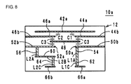
- Fig. 8 is a cross-sectional view of a multilayer electronic component 10a that is an exemplary modification of a multilayer electronic component according to the present invention.
- the via-hole conductors 54 and 62 may be aligned.
- the internal electrode 58 is not required.
- a widthwise direction on the upper surface of the multilayer electronic component 10b is hereinafter referred to as an x-axis direction
- a lengthwise direction on the upper surface of the multilayer electronic component 10b is hereinafter referred to as a y-axis direction
- a lamination direction of the multilayer electronic component 10b is hereinafter referred to as a z-axis direction.
- Fig. 3 is also used as the equivalent circuit diagram of the multilayer electronic component 10b.
- the multilayer electronic component 10b includes the laminate 12, the input external electrode 14a, the output external electrode 14b, the ground external electrodes 16a and 16b, and the orientation recognition mark 18.
- the laminate 12 is formed by laminating a plurality of insulating layers, and is a rectangular parallelepiped. In the laminate 12, a plurality of capacitors (not illustrated) and a plurality of inductors (not illustrated) are formed.
- the input external electrode 14a is formed on an end face located at an end portion of the laminate 12 in the y-axis direction, and functions as a terminal for receiving a signal.
- the output external electrode 14b is formed on an end face facing the end face on which the input external electrode 14a is formed, and functions as a terminal for outputting a signal.
- the ground external electrode 16a is formed on a side surface located at an end portion of the laminate 12 in the x-axis direction.
- the ground external electrode 16b is formed on a side surface facing the side surface on which the ground external electrode 16a is formed.
- the orientation recognition mark 18 is formed on the upper surface of the laminate 12, and is used to recognize the orientation of the multilayer electronic component 10b.
- insulating layers 140, 136, 134a to 134f, 132, 130a to 130g, 128, 126, 124, 122, 120a, and 120b are laminated so that these insulating layers are arranged in this order from top to bottom (the insulating layers 130d to 30f, 134d, and 134e are not illustrated). If the insulating layers 130a to 130g and 134a to 134f are differentiated from each other, the insulating layers 130a to 130g and 134a to 134f are used. If the insulating layers 130a to 130g and the insulating layers 134a to 134f are correctively called, the insulating layers 130 and 134 are used, respectively.
- the internal electrode 142 includes a capacitor electrode 142a and extraction electrodes 142b and 142c.
- the capacitor electrode 142a is a rectangular electrode formed on the main surface of the insulating layer 122, and functions as one electrodes of the capacitors C1 and C2 as illustrated in Figs. 3 and 11 .
- One end of the extraction electrode 142b is connected to the capacitor electrode 142a, and the other end of the extraction electrode 142b is connected to the ground external electrode 16a illustrated in Fig. 9 .
- One end of the extraction electrode 142c is connected to the capacitor electrode 142a, and the other end of the extraction electrode 142c is connected to the ground external electrode 16b illustrated in Fig. 9 . Therefore, the internal electrode 142 also functions as a ground electrode.
- the internal electrode 144 includes a capacitor electrode 144a and an extraction electrode 144b.
- the capacitor electrode 144a is a rectangular electrode formed on the main surface of the insulating layer 124 so that it faces the capacitor electrode 142a, and functions as the other electrode of the capacitor C1 as illustrated in Figs. 3 and 11 . Furthermore, the capacitor electrode 144a also functions as one electrode of the capacitor C3. One end of the extraction electrode 144b is connected to the capacitor electrode 144a, and the other end of the extraction electrode 144b is connected to the output external electrode 14b illustrated in Fig. 9 .
- the internal electrode 146 includes a capacitor electrode 146a and an extraction electrode 146b.
- the capacitor electrode 146a is a rectangular electrode formed on the main surface of the insulating layer 124 so that it faces the capacitor electrode 142a, and functions as the other electrode of the capacitor C2 as illustrated in Figs. 3 and 11 . Furthermore, the capacitor electrode 146a also functions as the other electrode of the capacitor C3. That is, the capacitor electrodes 144a and 146a form the capacitor C3.
- One end of the extraction electrode 146b is connected to the capacitor electrode 146a, and the other end of the extraction electrode 146b is connected to the input external electrode 14a illustrated in Fig. 9 .
- an internal electrode (capacitor electrode) 148 is formed on the main surface of the insulating layer 126 so that it faces the capacitor electrodes 144a and 146b, and functions as a part of the capacitor C3 as illustrated in Figs. 3 and 11 .
- the internal electrode 150 includes a capacitor electrode 150a and an extraction electrode 150b.
- the capacitor electrode 150a is a rectangular electrode formed on the main surface of the insulating layer 128, and functions as one electrode of the capacitor C3 as illustrated in Figs. 3 and 11 .
- One end of the extraction electrode 150b is connected to the capacitor electrode 150a, and the other end of the extraction electrode 150b is connected to the output external electrode 14b illustrated in Fig. 9 .
- the internal electrode 152 includes a capacitor electrode 152a and an extraction electrode 152b.
- the capacitor electrode 152a is a rectangular electrode formed on the main surface of the insulating layer 128, and functions as the other electrode of the capacitor C3 as illustrated in Figs. 3 and 11 . That is, the capacitor electrodes 150a and 152a form the capacitor C3.
- One end of the extraction electrode 152b is connected to the capacitor electrode 152a, and the other end of the extraction electrode 152b is connected to the input external electrode 14a illustrated in Fig. 9 .
- via-hole conductors 154a to 154g and via-hole conductors 156a to 156g are formed, respectively (the via-hole conductors 154b to 154g and 156b to 156g are not illustrated).
- via-hole conductors 159 and 161 are formed in the insulating layer 132.
- the via-hole conductors 154a to 154g and 159 are formed as a first interlayer connection conductor extending in the lamination direction in the laminate 12 and functions as the inductor L1A as illustrated in Figs. 3 and 11 .
- the via-hole conductors 156a to 156g and 161 are formed as a third interlayer connection conductor extending in the lamination direction in the laminate 12 and functions as the inductor L2A as illustrated in Figs. 3 and 11 .
- the via-hole conductors 154g and 156g are directly connected to the capacitor electrodes 150a and 152a, respectively.
- the via-hole conductors 154a to 154g and the via-hole conductors 156a to 156g are used, respectively.
- via-hole conductors 154 and 156 are used, respectively.
- the via-hole conductors 154a to 154g and 159 and the via-hole conductors 156a to 156g and 161 are formed on the insulating layers 130a to 130g and 132 so that they are apart from each other by the first distance D1, respectively.
- the insulating layers 130a to 130g In [the main surfaces of] the insulating layers 130a to 130g, only the via-hole conductors 154a to 154g and only the via-hole conductors 156a to 156g are formed, respectively.
- the insulating layers 130a to 130g are members having the same structure.
- the internal electrode 158 is a rectangular electrode formed on the main surface of the insulating layer 132, and is connected to the via-hole conductor 159.
- the internal electrode 160 is a rectangular electrode formed on the main surface of the insulating layer 132, and is connected to the via-hole conductor 161.
- the internal electrodes 158 and 160 are used to shift the positions of the inductors L1C and L2C electrically connected to the inductors L1A and L2A so that the inductors L1C and L2C and the inductors L1A and L2A are not aligned, respectively, in the xy plane.
- the internal electrodes 158 and 160 also function as the inductors L1B and L2B, respectively.
- via-hole conductors 162a to 162f and via-hole conductors 164a to 164f are formed, respectively (the via-hole conductors 162b to 162f and 164b to 164f are not illustrated).
- via-hole conductors 167 and 169 are formed in the insulating layer 136.
- the insulating layers 134a to 134f are members having the same structure. By laminating the insulating layers 134a to 134f and 136, the via-hole conductors 162a to 162f and 167 are formed as a second interlayer connection conductor extending in the lamination direction in the laminate 12 and functions as the inductor L1C.
- the via-hole conductors 164a to 164f and 169 are formed as a fourth interlayer connection conductor extending in the lamination direction in the laminate 12 and functions as the inductor L2C.
- the via-hole conductors 162f and 164f are connected to the internal electrodes 158 and 161, respectively.
- the via-hole conductors 162a to 162f and the via-hole conductors 164a to 164f are used, respectively.
- via-hole conductors 162 and 164 are used, respectively.
- the via-hole conductors 162a to 162f and 167 and the via-hole conductors 164a to 164f and 169 are formed on the insulating layers 134a to 134f and 136 so that they are apart from each other by the second distance D2 that is shorter than the first distance D1, respectively.
- the via-hole conductors 162a to 162f and 167 are formed, respectively.
- the internal electrode 166 includes inductor electrodes 166a and 166b and an extraction electrode 166c, and functions as a common electrode.
- Each of the inductor electrodes 166a and 166b is a rectangular electrode formed on the main surface of the insulating layer 136, and functions as the inductor L3 along with the ground external electrode 16b.
- One ends of the inductor electrodes 166a and 166b are connected to the via-hole conductors 167 and 169, respectively.
- the inductors L1C and L2C are electrically connected to each other via the internal electrode 166.
- One end of the extraction electrode 166c is connected to the inductor electrodes 166a and 166b, and the other end of the extraction electrode 166c is connected to the ground external electrode 16a.
- the internal electrode 168 is formed along a side facing a side at which the extraction electrode 166c is formed.
- the internal electrode 168 is formed so that it is apart from the inductor electrodes 166a and 166b by a predetermined distance, and one end of the internal electrode 168 is connected to the ground external electrode 16b.
- the multilayer electronic component 10b having an equivalent circuit illustrated in Fig. 3 and a cross section structure illustrated in Fig. 11 is obtained.
- the multilayer electronic component 10b having the above-described structure can provide the same operational effect as that of the multilayer electronic component 10a.
- the equivalent circuit of the multilayer electronic component 10b is the same as that of the multilayer electronic component 10, and the description thereof will be therefore omitted. Furthermore, a method of manufacturing the multilayer electronic component 10b is basically the same as the method of manufacturing the multilayer electronic component 10, and the description thereof will be therefore omitted.
- the present invention is useful for a multilayer electronic component and a multilayer electronic component manufacturing method, and, in particular, has an advantage in its suitability for easily controlling the degree of magnetic field coupling between inductors.
Landscapes
- Engineering & Computer Science (AREA)
- Power Engineering (AREA)
- Manufacturing & Machinery (AREA)
- Microelectronics & Electronic Packaging (AREA)
- Physics & Mathematics (AREA)
- Electromagnetism (AREA)
- Filters And Equalizers (AREA)
- Coils Or Transformers For Communication (AREA)
- Fixed Capacitors And Capacitor Manufacturing Machines (AREA)
Abstract
Description
- The present invention relates to multilayer electronic components and multilayer electronic component manufacturing methods, and, more particularly, to a multilayer electronic component including a resonance circuit and a multilayer electronic component manufacturing method of manufacturing such a multilayer electronic component.
-
Patent Documents - However, if the distance between these via-hole conductors is adjusted or a new via-hole conductor is added, it is necessary to redesign an electronic component with built-in inductors and a multilayer LC component. This requires a very complicated operation. More specifically, it is necessary to change a punching program for forming a via-hole conductor in a ceramic green sheet included in an electronic component with built-in inductors and a multilayer LC component, reset an apparatus for punching the ceramic green sheet, and manufacture a new metal mold used to punch the ceramic green sheet.
- [Patent Document 1] Japanese Unexamined Patent Application Publication No.
09-35936 - [Patent Document 2] Japanese Unexamined Patent Application Publication No.
2002-57543 - It is an object of the present invention to provide a multilayer electronic component and a multilayer electronic component manufacturing method capable of easily controlling the degree of magnetic field coupling between inductors. Means for Solving the Problems
- A multilayer electronic component according to the present invention includes: a laminate formed by laminating a plurality of insulating layers including a first insulating layer and a second insulating layer; a first capacitor and a second capacitor which are formed in the laminate; a first interlayer connection conductor and a second interlayer connection conductor which extend in a lamination direction in the laminate and function as a first inductor; and a third interlayer connection conductor and a fourth interlayer connection conductor which extend in the lamination direction in the laminate and function as a second inductor that is coupled to the first inductor by magnetic field coupling. The first capacitor and the first inductor form a first resonance circuit, and the second capacitor and the second inductor form a second resonance circuit. The first interlayer connection conductor and the third interlayer connection conductor are formed in the first insulating layer so that they are apart from each other by a first distance. The second interlayer connection conductor and the fourth interlayer connection conductor are formed in the second insulating layer so that they are apart from each other by a second distance that is different from the first distance.
- According to the present invention, since there are two types of distances between interlayer connection conductors, it is possible to adjust the average of the length of the first inductor and the length of the second inductor by changing the lengths of the first interlayer connection conductor, the second interlayer connection conductor, the third interlayer connection conductor, and the fourth interlayer connection conductor. As a result, it is possible to control the degree of magnetic field coupling between the first inductor and the second inductor.
- In the present invention, only the first interlayer connection conductor and only the third interlayer connection conductor may be formed in a main surface of the first insulating layer, and only the second interlayer connection conductor and only the fourth interlayer connection conductor may be formed in a main surface of the second insulating layer.
- In the present invention, the multilayer electronic component may further include a ground electrode formed in the laminate. In the lamination direction, the first capacitor may be located between the first inductor and the ground electrode and the second capacitor may be located between the second inductor and the ground electrode.
- In the present invention, the multilayer electronic component may further include a common electrode formed in the laminate. The first interlayer connection conductor and the second interlayer connection conductor may be electrically connected to each other. The third interlayer connection conductor and the fourth interlayer connection conductor may be electrically connected to each other. The first interlayer connection conductor may be connected to the first capacitor. The third interlayer connection conductor may be connected to the second capacitor. The second interlayer connection conductor and the fourth interlayer connection conductor may be electrically connected to each other via the common electrode.
- The present invention can be applied to a multilayer electronic component manufacturing method. More specifically, a multilayer electronic component manufacturing method according to the present invention is a method of manufacturing a multilayer electronic component including a first resonance circuit composed of a first capacitor and a first inductor and a second resonance circuit composed of a second capacitor and a second inductor. The multilayer electronic component manufacturing method includes: a first step of forming a first interlayer connection conductor functioning as the first inductor and a third interlayer connection conductor functioning as the second inductor in a first insulating layer so that they are apart from each other by a first distance; a second step of forming a second interlayer connection conductor functioning as the first inductor and a fourth interlayer connection conductor functioning as the second inductor in a second insulating layer so that they are apart from each other by a second distance that is different from the first distance; and a third step of laminating the first insulating layer and the second insulating layer.
- In the present invention, in the third step, the number of the first insulating layers and the number of the second insulating layers may be controlled and then be laminated so as to control a characteristic of the multilayer electronic component.
- According to the present invention, since there are two types of distances between interlayer connection conductors, it is possible to control the degree of magnetic field coupling between the first inductor and the second inductor by changing the lengths of the first interlayer connection conductor and the second interlayer connection conductor, and by changing the lengths of the third interlayer connection conductor and the fourth interlayer connection conductor.
-
- [
Fig. 1] Fig. 1(a) is a diagram illustrating a multilayer electronic component according to a first embodiment as viewed from the upper surface of the multilayer electronic component.Fig. 1(b) is a diagram illustrating the multilayer electronic component as viewed from the undersurface of the multilayer electronic component. - [
Fig. 2] Fig. 2 is an exploded perspective view of the laminate included in the multilayer electronic component illustrated inFig. 1 . - [
Fig. 3] Fig. 3 is an equivalent circuit diagram of the multilayer electronic component. - [
Fig. 4] Fig. 4 is a cross-sectional view of the multilayer electronic component taken along the line A-A ofFig. 1 . - [
Fig. 5] Fig. 5(a) is a graph illustrating the loss characteristic of the first pattern of the multilayer electronic component.Fig. 5(b) is a graph illustrating the loss characteristic of the second pattern of the multilayer electronic component.Fig. 5(c) is a graph illustrating the loss characteristic of the third pattern of the multilayer electronic component. - [
Fig. 6] Fig. 6 is a diagram illustrating a ceramic green sheet used as an insulating layer. - [
Fig. 7] Fig. 7 is a graph illustrating the loss characteristic of the multilayer electronic component. - [
Fig. 8] Fig. 8 is a cross-sectional view of a multilayer electronic component that is an exemplary modification of a multilayer electronic component according to the present invention. - [
Fig. 9] Fig. 9(a) is a diagram illustrating a multilayer electronic component according to a second embodiment as viewed from the upper surface of the multilayer electronic component.Fig. 9(b) is a diagram illustrating the multilayer electronic component as viewed from the undersurface of the multilayer electronic component. - [
Fig. 10] Fig. 10 is an exploded perspective view of the laminate included in the multilayer electronic component illustrated inFig. 9 . - [
Fig. 11] Fig. 11 is a cross-sectional view of the multilayer electronic component taken along the line A-A ofFig. 9 . - A multilayer electronic component and a multilayer electronic component manufacturing method according to an embodiment of the present invention will be described below.
- A multilayer electronic component according to the first embodiment of the present invention will be described with reference to the accompanying drawings.
Fig. 1 is an external perspective view of a multilayerelectronic component 10 according to the first embodiment of the present invention. More specifically,Fig. 1(a) is a diagram illustrating the multilayerelectronic component 10 as viewed from the upper surface of the multilayerelectronic component 10.Fig. 1(b) is a diagram illustrating the multilayerelectronic component 10 as viewed from the undersurface of the multilayerelectronic component 10.Fig. 2 is an exploded perspective view of alaminate 12 included in the multilayerelectronic component 10.Fig. 3 is an equivalent circuit diagram of the multilayerelectronic component 10.Fig. 4 is a cross-sectional view of the multilayerelectronic component 10 taken along the line A-A illustrated ofFig. 1 . As illustrated inFig. 1 , a widthwise direction on the upper surface of the multilayerelectronic component 10 is hereinafter referred to as an x-axis direction, a lengthwise direction on the upper surface of the multilayerelectronic component 10 is hereinafter referred to as a y-axis direction, and a lamination direction of the multilayerelectronic component 10 is hereinafter referred to as a z-axis direction. - First, the external view of the multilayer
electronic component 10 will be described with reference toFig. 1 . The multilayerelectronic component 10 includes thelaminate 12, an inputexternal electrode 14a, an outputexternal electrode 14b, groundexternal electrodes 16a and 16b, and anorientation recognition mark 18. Thelaminate 12 is formed by laminating a plurality of insulating layers, and is a rectangular parallelepiped. In thelaminate 12, a plurality of capacitors (not illustrated) and a plurality of inductors (not illustrated) are formed. The inputexternal electrode 14a is formed on an end face located at an end portion of the laminate 12 in the y-axis direction, and functions as a terminal for receiving a signal. The outputexternal electrode 14b is formed on an end face facing the end face on which the inputexternal electrode 14a is formed, and functions as a terminal for outputting a signal. - The ground external electrode 16a is formed on a side surface located at an end portion of the laminate 12 in the x-axis direction. The ground
external electrode 16b is formed on a side surface facing the side surface on which the ground external electrode 16a is formed. Theorientation recognition mark 18 is formed on the undersurface of the laminate 12, and is used to recognize the orientation of the multilayerelectronic component 10. - Next, the inner structure of the laminate 12 will be described with reference to
Figs. 2 to 4 . As illustrated inFig. 2 , in the laminate 12, insulatinglayers layers - On the main surfaces of the insulating
layers 20a and 20b, no component is formed. On the main surface of the insulatinglayer 22, aninternal electrode 42 is formed.
Theinternal electrode 42 includes a capacitor electrode 42a andextraction electrodes layer 22, and functions as one electrodes of capacitors C1 and C2 as illustrated inFigs. 3 and 4 . One end of theextraction electrode 42b is connected to the capacitor electrode 42a, and the other end of theextraction electrode 42b is connected to the ground external electrode 16a illustrated inFig. 1 . One end of theextraction electrode 42c is connected to the capacitor electrode 42a, and the other end of theextraction electrode 42c is connected to the groundexternal electrode 16b illustrated inFig. 1 . Therefore, theinternal electrode 42 also functions as a ground electrode. - On the main surface of the insulating
layer 24,internal electrodes internal electrode 44 includes a capacitor electrode 44a and anextraction electrode 44b. The capacitor electrode 44a is a rectangular electrode formed on the main surface of the insulatinglayer 24 so that it faces the capacitor electrode 42a, and functions as the other electrode of the capacitor C1 as illustrated inFigs. 3 and 4 . Furthermore, the capacitor electrode 44a also functions as one electrode of a capacitor C3. One end of theextraction electrode 44b is connected to the capacitor electrode 44a, and the other end of theextraction electrode 44b is connected to the outputexternal electrode 14b illustrated inFig. 1 . - The
internal electrode 46 includes acapacitor electrode 46a and anextraction electrode 46b. Thecapacitor electrode 46a is a rectangular electrode formed on the main surface of the insulatinglayer 24 so that it faces the capacitor electrode 42a, and functions as the other electrode of the capacitor C2 as illustrated inFigs. 3 and 4 . Furthermore, thecapacitor electrode 46a also functions as the other electrode of the capacitor C3. That is, thecapacitor electrodes 44a and 46a form the capacitor C3. One end of theextraction electrode 46b is connected to thecapacitor electrode 46a, and the other end of theextraction electrode 46b is connected to the inputexternal electrode 14a illustrated inFig. 1 . - On the main surface of the insulating layer 26, an internal electrode (capacitor electrode) 48 is formed. The
capacitor electrode 48 is a rectangular electrode formed on the main surface of the insulating layer 26 so that it faces thecapacitor electrodes 44a and 46a, and functions as a part of the capacitor C3 as illustrated inFigs. 3 and 4 . - On the main surface of the insulating
layer 28,internal electrodes internal electrode 50 includes acapacitor electrode 50a and anextraction electrode 50b. Thecapacitor electrode 50a is a rectangular electrode formed on the main surface of the insulatinglayer 28, and functions as one electrode of the capacitor C3 as illustrated inFigs. 3 and 4 . One end of theextraction electrode 50b is connected to thecapacitor electrode 50a, and the other end of theextraction electrode 50b is connected to the outputexternal electrode 14b illustrated inFig. 1 . - The
internal electrode 52 includes acapacitor electrode 52a and anextraction electrode 52b. Thecapacitor electrode 52a is a rectangular electrode formed on the main surface of the insulatinglayer 28, and functions as the other electrode of the capacitor C3 as illustrated inFigs. 3 and 4 . That is, thecapacitor electrodes extraction electrode 52b is connected to thecapacitor electrode 52a, and the other end of theextraction electrode 52b is connected to the inputexternal electrode 14a illustrated inFig. 1 . - In addition, in the insulating
layer 28, via-hole conductors 51 and 53 are formed. The via-hole conductors 51 and 53 are directly connected to thecapacitor electrodes - In the insulating layers 30a to 30g, via-hole conductors 54a to 54g and via-hole conductors 56a to 56g are formed, respectively (the via-hole conductors 54b to 54g and 56b to 56g are not illustrated). The insulating layers 30a to 30g are members having the same structure. By laminating the insulating
layers 28 and 30a to 30g, the via-hole conductors 51 and 54a to 54g are formed as a first interlayer connection conductor extending in the lamination direction in the laminate 12, and functions as an inductor L1A as illustrated inFigs. 3 and 4 . By laminating the insulatinglayers 28 and 30a to 30g, the via-hole conductors 53 and 56a to 56g are formed as a third interlayer connection conductor extending in the lamination direction in the laminate 12, and functions as an inductor L2A as illustrated inFigs. 3 and 4 . In order to represent via-hole conductors formed on the insulating layers 30a to 30g, the via-hole conductors 54a to 54g and the via-hole conductors 56a to 56g are used, respectively. In order to represent a via-hole conductor obtained by connecting the via-hole conductors 51 and 54a to 54g to each other and a via-hole conductor obtained by connecting the via-hole conductors 53 and 56a to 56g to each other, via-hole conductors - Furthermore, the via-
hole conductors 51 and 54a to 54g and the via-hole conductors 53 and 56a to 56g are formed in the insulatinglayers 28 and 30a to 30g so that they are apart from each other by a first distance D1, respectively. In the main surfaces of the insulating layers 30a to 30g, only the via-hole conductors 54a to 54g and only the via-hole conductors 56a to 56g are formed, respectively. - On the main surface of the insulating
layer 32,internal electrodes internal electrode 58 is a rectangular electrode formed on the main surface of the insulatinglayer 32, and is connected to the via-hole conductor 54. Theinternal electrode 60 is a rectangular electrode formed on the main surface of the insulatinglayer 32, and is connected to the via-hole conductor 56. - Furthermore, in the insulating
layer 32, via-hole conductors hole conductors internal electrodes Figs. 3 and 4 , theinternal electrodes Figs. 3 and 4 , theinternal electrodes - In the insulating layers 34a to 34f, via-hole conductors 62a to 62f and via-hole conductors 64a to 64f are formed, respectively (the via-hole conductors 62b to 62f and 64b to 64f are not illustrated). The insulating layers 34a to 34f are members having the same structure. By laminating the insulating
layers 32 and 34a to 34f, the via-hole conductors 59 and 62a to 62f are formed as a second interlayer connection conductor extending in the lamination direction in the laminate 12 and functions as the inductor L1C. By laminating the insulatinglayers 32 and 34a to 34f, the via-hole conductors 61 and 64a to 64f are formed as a fourth interlayer connection conductor extending in the lamination direction in the laminate 12 and functions as the inductor L2C. In order to represent via-hole conductors formed on the insulating layers 34a to 34f, the via-hole conductors 62a to 62f and the via-hole conductors 64a to 64f are used, respectively. In order to represent a via-hole conductor obtained by connecting the via-hole conductors 59 and 62a to 62f to each other and a via-hole conductor obtained by connecting the via-hole conductors 61 and 64a to 64f to each other, via-hole conductors - Furthermore, the via-
hole conductors 59 and 62a to 62f and the via-hole conductors 61 and 64a to 64f are formed on the insulatinglayers 32 and 34a to 34f so that they are apart from each other by a second distance D2 that is shorter than the first distance D1, respectively. In the main surfaces of the insulating layers 34a to 34f, only the via-hole conductors 62a to 62f and only the via-hole conductors 64a to 64f are formed, respectively. - On the main surface of the insulating
layer 36,internal electrodes internal electrode 66 includesinductor electrodes 66a and 66b and anextraction electrode 66c, and functions as a common electrode. Each of theinductor electrodes 66a and 66b is a rectangular electrode formed on the main surface of the insulatinglayer 36, and functions as an inductor L3 along with the groundexternal electrode 16b. One ends of theinductor electrodes 66a and 66b are connected to the via-hole conductors extraction electrode 66c is connected to theinductor electrodes 66a and 66b, and the other end of theextraction electrode 66c is connected to the ground external electrode 16a. As a result, the inductors L1C and L2C are electrically connected to each other via theinternal electrode 66. - The
internal electrode 68 is formed along a side facing a side at which theextraction electrode 66c is formed. Theinternal electrode 68 is formed so that it is apart from theinductor electrodes 66a and 66b by a predetermined distance, and one end of theinternal electrode 68 is connected to the groundexternal electrode 16b. - On the main surface of the insulating
layer 38, no component is formed. On the undersurface of the insulatinglayer 40, - By laminating the insulating
layers electronic component 10 having an equivalent circuit illustrated inFig. 3 and a cross section structure illustrated inFig. 4 is obtained. - The equivalent circuit illustrated in
Fig. 3 will be described. The equivalent circuit of the multilayerelectronic component 10 includes the capacitors C1, C2, and C3, the inductors L1A, L1B, L1C, L2A, L2B, L2C, and L3, an input terminal P1, and an output terminal P2, and forms a band-pass filter. The input terminal P1 corresponds to the inputexternal electrode 14a illustrated inFig. 1 , and the output terminal P2 corresponds to the outputexternal electrode 14b illustrated inFig. 1 . - The capacitor C1 and the inductors L1A, L1B, and L1C are connected in parallel with each other, so that a resonance circuit LC1 is formed. The capacitor C2 and the inductors L2A, L2B, and L2C are connected in parallel with each other, so that a resonance circuit LC2 is formed. One end of the resonance circuit LC1 is connected to the input terminal P1, and the other end of the resonance circuit LC1 is connected to the inductor L3. One end of the resonance circuit LC2 is connected to the output terminal P2, and the other end of the resonance circuit LC2 is connected to the inductor L3. One end of the inductor L3 is connected to the ground. That is, the other end of the inductor L3 corresponds to the ground
external electrodes 16a and 16b. Furthermore, between the input terminal P1 and the output terminal P2, the capacitor C3 for coupling the resonance circuits LC1 and LC2 to each other is disposed. - In the multilayer
electronic component 10 having the above-described structure, a mutual inductance M1 is generated between the inductors L1A and L2A, and a mutual inductance M2 is generated between the inductors L1C and L2C. As a result, the resonance circuits LC1 and LC2 are coupled to each other by magnetic field coupling. The degree of magnetic field coupling between the resonance circuits LC1 and LC2 depends on the lengths of the via-hole conductors Figs. 2 and4 and the distances D1 and D2. Accordingly, in the multilayerelectronic component 10, by controlling the number of the insulatinglayers 30 and the number of the insulatinglayers 34, a band-pass filter having a desired characteristic can be obtained. The processing for controlling the number of the insulatinglayers 30 and the number of the insulatinglayers 34 will be described later. - Next, a method of manufacturing the multilayer
electronic component 10 will be described with reference toFigs. 1 and2 . - First, ceramic green sheets used as the insulating
layers - A binding agent (for example, vinyl acetate or watersoluble acrylic), a plasticizing agent, a wetting agent, and a dispersing agent are mixed with the ceramic powder in the ball mill. Subsequently, an obtained mixture is subjected to defoaming by decompression, so that ceramic slurry is obtained. The ceramic slurry is formed into the shape of a sheet using the doctor blade method and is then dried, so that a ceramic green sheet having a desired film thickness is obtained.
- Subsequently, in the insulating
layers 28 and 30a to 30g that are ceramic green sheets, the via-hole conductors 51 and 54a to 54g and the via-hole conductors 53 and 56a to 56g, which are illustrated inFig. 2 , are formed so that they are apart from each other by the first distance D1, respectively. More specifically, a through-hole is formed in a ceramic green sheet using laser beam and conductive paste including Ag, Pd, Cu, Au, or an alloy thereof is then filled in the through-hole by printing or the like, so that the via-hole conductors 51, 54a to 54g, 53, and 56a to 56g are formed. - Subsequently, in the insulating
layers 32 and 34a to 34f that are ceramic green sheets, the via-hole conductors 59 and 62a to 62f and the via-hole conductors 61 and 64a to 64f, which are illustrated inFig. 2 , are formed so that they are apart from each other by the second distance D2, respectively. The detailed method of forming the via-hole conductors hole conductors 51, 53, 54a to 54g, and 56a to 56g, and the description thereof is therefore omitted. - Subsequently, on the main surfaces of the insulating
layers internal electrodes layer 40 that is a ceramic green sheet, - Subsequently, an uncalcined mother laminate is formed by laminating ceramic green sheets. At that time, in order to obtain a band-pass filter having desired characteristics (such as a bandwidth and an attenuation characteristic), the lengths of the via-
hole conductors layers 30 and the number of the insulating layers 34. A predetermined number of ceramic green sheets are temporarily press-bonded. After the temporal press bonding of these ceramic green sheets has been completed, the full press bonding of the mother laminate is performed using a hydrostatic pressure or the like. - Subsequently, the uncalcined mother laminate is cut into separate laminates by a dicing machine or the like, so that rectangular parallelepiped laminates are obtained.
- Subsequently, the laminates are subjected to binder removing processing and calcination, so that a calcined laminate, the laminate 12, is obtained.
- Subsequently, using a known method such as a dipping method, the surface of the laminate 12 is subjected to the application of electrode paste including silver, copper, or palladium as a main component and baking, so that a silver, copper, or palladium electrode having a shape illustrated in
Fig. 1 is formed. - Finally, the surface of the baked silver, copper, or palladium electrode is subjected to Ni plating and Sn plating or is subjected to Ni plating and solder plating, so that the input
external electrode 14a, the outputexternal electrode 14b, the groundexternal electrodes 16a and 16b, and theorientation recognition mark 18 are formed. After the above-described process has been performed, the multilayerelectronic component 10 illustrated inFig. 1 is manufactured. - Although a sheet lamination method has been described, a method of manufacturing the multilayer
electronic component 10 is not limited thereto. For example, the multilayerelectronic component 10 may be manufactured using a printing lamination method or a transfer lamination method. - According to the multilayer
electronic component 10 and the method of manufacturing the multilayerelectronic component 10, it is possible to easily change the degree of coupling between the inductors L1A and L2A and the degree of coupling between the inductors L1C and L2C, and to easily obtain the multilayerelectronic component 10 having various characteristics. The detailed description thereof will be made below. - In the electronic component with built-in inductors disclosed in
Patent Document 1 and the multilayer LC component disclosed inPatent Document 2, in order to provide various characteristics for the electronic component with built-in inductors and the multilayer LC component, the degree of magnetic field coupling between the inductors is changed using a method of adjusting the distance between via-hole conductors or a method of adding a via-hole conductor. However, if these methods are used, it is required to redesign the electronic component with built-in inductors and the multilayer LC component. This requires a very complicated operation. More specifically, it is necessary to change a punching program for forming a via-hole conductor in a ceramic green sheet included in the electronic component with built-in inductors and the multilayer LC component, reset an apparatus for punching the ceramic green sheet, and create a new metal mold used to punch the ceramic green sheet. - On the contrary, according to the multilayer
electronic component 10 and the method of manufacturing the multilayerelectronic component 10, only by controlling the number of the insulatinglayers 30 to be laminated and the number of the insulatinglayers 34 to be laminated, it is possible to adjust the lengths of the via-hole conductors layers 30 and the number of the insulatinglayers 34 are controlled, the multilayerelectronic component 10 having a plurality of types of characteristics can be obtained. An example of the method of manufacturing the multilayerelectronic component 10 will be described with reference to Table 1 andFig. 5 . -
Table 1 insulating layer thickness (µm) the number of insulating layers first pattern second pattern third pattern insulating layer 20 25 2 2 2 insulating layer 2225 1 1 1 insulating layer 2425 1 1 1 insulating layer 26 25 1 1 1 insulating layer 2825 1 1 1 insulating layer 3025 11 7 3 insulating layer 321 1 1 insulating layer 3425 2 6 10 insulating layer 3625 1 1 1 insulating layer 3840 1 1 1 insulating layer 4025 1 1 1 magnetic field coupling degree small normal large - Table 1 indicates the degree of magnetic field coupling between the inductors L1A and L2A and the degree of magnetic field coupling between the inductors L1C and L2C, when the number of the insulating
layers 30 and the number of the insulatinglayers 34 vary among three different values while the total number of insulating layers is not changed. More specifically, in the first pattern of the multilayerelectronic component 10, the eleven insulatinglayers 30 and the two insulatinglayers 34 are laminated. In the second pattern of the multilayerelectronic component 10, the seven insulatinglayers 30 and the six insulatinglayers 34 are laminated. The multilayerelectronic component 10 illustrated inFig. 2 corresponds to the second pattern of the multilayerelectronic component 10. In the third pattern of the multilayerelectronic component 10, the three insulatinglayers 30 and the ten insulatinglayers 34 are laminated.Fig. 5(a) is a graph illustrating the loss characteristic of the first pattern of the multilayerelectronic component 10.Fig. 5(b) is a graph illustrating the loss characteristic of the second pattern of the multilayerelectronic component 10.Fig. 5(c) is a graph illustrating the loss characteristic of the third pattern of the multilayerelectronic component 10. In these graphs, a vertical axis represents a loss, and a horizontal axis represents a frequency. - If the lengths of the via-
hole conductors electronic component 10 are standard lengths, the length of the via-hole conductors hole conductors electronic component 10. Accordingly, the average distance between the inductors L1A, L1C and the inductors L2A, L2C in the first pattern of the multilayerelectronic component 10 is greater than the average distance between the inductors L1A, L1C and the inductors L2A, L2C in the second pattern of the multilayerelectronic component 10. As a result, as illustrated in Table 1, the degree of magnetic field coupling of the first pattern of the multilayerelectronic component 10 is less than that of the second pattern of the multilayerelectronic component 10. Accordingly, as illustrated inFigs. 5(a) and 5(b) , the first pattern of the multilayerelectronic component 10 is a band-pass filter having a filter characteristic of a narrower band than that of the second pattern of the multilayerelectronic component 10. - On the other hand, in the third pattern of the multilayer
electronic component 10, the length of the via-hole conductors hole conductors electronic component 10 is less than the average distance between the inductors L1A, L1C and the inductors L2A, L2C in the second pattern of the multilayerelectronic component 10. As a result, as illustrated in Table 1, the degree of magnetic field coupling of the third pattern of the multilayerelectronic component 10 is greater than that of the second pattern of the multilayerelectronic component 10. Accordingly, as illustrated inFigs. 5(b) and 5(c) , the third pattern of the multilayerelectronic component 10 is a band-pass filter having a filter characteristic of a wider band than that of the second pattern of the multilayerelectronic component 10. - In the multilayer
electronic component 10, since theinternal electrode 68 is disposed as illustrated inFig. 2 , it is possible to suppress the variations in the potentials of theinductor electrodes 66a and 66b. Descriptions thereof will be made below with reference toFig. 6. Fig. 6 is a diagram illustrating a ceramic green sheet used as the insulatinglayer 36. - If the
internal electrode 68 is not present, the potentials of theinductor electrodes 66a and 66b are most strongly affected by the potential of the groundexternal electrode 16b that is nearest to theinductor electrodes 66a and 66b. Since the groundexternal electrode 16b is formed by screen printing or the like, a position at which the groundexternal electrode 16b is formed varies within the margin of a manufacturing error. Furthermore, positions at which theinductor electrodes 66a and 66b are formed vary within the margin of a manufacturing error. Consequently, the distance between the groundexternal electrode 16b and each of theinductor electrodes 66a and 66b varies, resulting in the variation in the effect of the potential of the groundexternal electrode 16b on the potentials of theinductor electrodes 66a and 66b. - In the multilayer
electronic component 10, theinternal electrode 68 to which a ground potential is applied is formed at a position apart from theinductor electrodes 66a and 66b by a predetermined distance. As a result, the potentials of theinductor electrodes 66a and 66b are most strongly affected by the potential of theinternal electrode 68. Accordingly, theinductor electrodes 66a and 66b are not easily affected by the groundexternal electrodes 16a and 16b. - Furthermore, as illustrated in
Fig. 6 , theinternal electrodes 68 that are individually connected to theinternal electrodes 66 are formed at predetermined intervals by screen printing or the like on a ceramic green sheet. Subsequently, the ceramic green sheet is cut, so that theinternal electrodes 66 are individually separated from theinternal electrodes 68. Accordingly, even if cut positions of the ceramic green sheet are changed, the distance between the internal electrodes 66 (each of theinductor electrodes 66a and 66b) and theinternal electrodes 68 is not changed. As a result, the variation in the effect of the potential of theinternal electrode 68 on the potential of theinternal electrode 66 is not easily produced. - In the multilayer
electronic component 10, the capacitor C3 is formed. Thus, by forming the capacitor C3, it is possible to abruptly change the both ends of a loss characteristic (to generate attenuation poles) as illustrated inFig. 7 that is a graph indicating the loss characteristic of the multilayerelectronic component 10.
As a result, the multilayerelectronic component 10 having a narrow-band filter characteristic can be obtained. - Furthermore, in the multilayer
electronic component 10, the inductor L3 is formed. By controlling the inductance of the inductor L3, it is possible to change the frequency of an attenuation pole on a higher frequency side from a dotted line to a solid line in the loss characteristic graph illustrated inFig. 7 . - Still furthermore, in the z-axis direction in the multilayer
electronic component 10, the capacitor C1 is disposed between theinternal electrode 42 and each of the inductors L1A to L1C, and the capacitor C2 is disposed between theinternal electrode 42 and each of the inductors L2A to L2C. As a result, as will be described later, the decrease in filter insertion loss is suppressed. More specifically, if the multilayerelectronic component 10 is disposed on a substrate so that the substrate is nearer to thecapacitor electrodes 44a and 46a than to theinternal electrode 42, thecapacitor electrodes 44a and 46a are hidden under theinternal electrode 42 and do not function as an antenna. Accordingly, the emission of a signal from thecapacitor electrodes 44a and 46a is suppressed, and the decrease in filter insertion loss is suppressed. - The present invention is not limited to the multilayer
electronic component 10 according to the above-described embodiment. Various changes can be made to the multilayerelectronic component 10 without departing from the spirit and scope of the present invention. - As the multilayer
electronic component 10, not only a band-pass filter but also a low-pass filter, a high-pass filter, or the like may be used. Alternatively, the multilayerelectronic component 10 may be a duplexer formed by the combination of band-pass filters, a low-pass filter, a high-pass filter, a trap circuit, or a duplexer formed by the combination of these different types of circuits. Alternatively, the multilayerelectronic component 10 may be not only a duplexer but also a triplexer or multiplexer including a plurality of filters in a single laminate or a triplexer or multiplexer including a filter and another circuit. Alternatively, the multilayerelectronic component 10 may be a coupler including a band-pass filter in which inductors formed by via-hole conductors and a coupling line are formed in an insulating layer lamination direction. - In the multilayer
electronic component 10, in order to adjust the length of the via-hole conductors hole conductors layers 30 and the number of the insulatinglayers 34 are controlled, respectively. However, a method of adjusting the length of the via-hole conductors hole conductors hole conductors hole conductors layer 30 and the thickness of the insulatinglayer 34 may be adjusted, respectively. -
Fig. 8 is a cross-sectional view of a multilayer electronic component 10a that is an exemplary modification of a multilayer electronic component according to the present invention. As illustrated in the multilayer electronic component 10a inFig. 8 , the via-hole conductors internal electrode 58 is not required. In the multilayer electronic component 10a, it is not required to shift the position of the via-hole conductor 62 using theinternal electrode 58 so that the via-hole conductors
This eliminates the problem of the disconnection between the via-hole conductors - A multilayer electronic component according to the second embodiment of the present invention will be described below with reference to the accompanying drawings.
Fig. 9 is an external perspective view of a multilayerelectronic component 10b according to the second embodiment. More specifically,Fig. 9(a) is a diagram illustrating the multilayerelectronic component 10b as viewed from the upper surface of the multilayerelectronic component 10b.Fig. 9(b) is a diagram illustrating the multilayerelectronic component 10b as viewed from the undersurface of the multilayerelectronic component 10b.Fig. 10 is an exploded perspective view of the laminate 12 included in the multilayerelectronic component 10b.Fig. 11 is a cross-sectional view of the multilayerelectronic component 10b taken along the line A-A illustrated ofFig. 9 . As illustrated inFig. 9 , a widthwise direction on the upper surface of the multilayerelectronic component 10b is hereinafter referred to as an x-axis direction, a lengthwise direction on the upper surface of the multilayerelectronic component 10b is hereinafter referred to as a y-axis direction, and a lamination direction of the multilayerelectronic component 10b is hereinafter referred to as a z-axis direction.Fig. 3 is also used as the equivalent circuit diagram of the multilayerelectronic component 10b. - First, the external view of the multilayer
electronic component 10b will be described with reference toFig. 9 . The multilayerelectronic component 10b includes the laminate 12, the inputexternal electrode 14a, the outputexternal electrode 14b, the groundexternal electrodes 16a and 16b, and theorientation recognition mark 18. The laminate 12 is formed by laminating a plurality of insulating layers, and is a rectangular parallelepiped. In the laminate 12, a plurality of capacitors (not illustrated) and a plurality of inductors (not illustrated) are formed. The inputexternal electrode 14a is formed on an end face located at an end portion of the laminate 12 in the y-axis direction, and functions as a terminal for receiving a signal. The outputexternal electrode 14b is formed on an end face facing the end face on which the inputexternal electrode 14a is formed, and functions as a terminal for outputting a signal. - The ground external electrode 16a is formed on a side surface located at an end portion of the laminate 12 in the x-axis direction. The ground
external electrode 16b is formed on a side surface facing the side surface on which the ground external electrode 16a is formed. Theorientation recognition mark 18 is formed on the upper surface of the laminate 12, and is used to recognize the orientation of the multilayerelectronic component 10b. - Next, the inner structure of the laminate 12 will be described with reference to
Figs. 10 and11 . As illustrated inFig. 10 , in the laminate 12, insulatinglayers layers - On the main surfaces of the insulating layers 120a and 120b, no component is formed. On the main surface of the insulating
layer 122, aninternal electrode 142 is formed. Theinternal electrode 142 includes a capacitor electrode 142a andextraction electrodes 142b and 142c. The capacitor electrode 142a is a rectangular electrode formed on the main surface of the insulatinglayer 122, and functions as one electrodes of the capacitors C1 and C2 as illustrated inFigs. 3 and11 . One end of the extraction electrode 142b is connected to the capacitor electrode 142a, and the other end of the extraction electrode 142b is connected to the ground external electrode 16a illustrated inFig. 9 . One end of theextraction electrode 142c is connected to the capacitor electrode 142a, and the other end of theextraction electrode 142c is connected to the groundexternal electrode 16b illustrated inFig. 9 . Therefore, theinternal electrode 142 also functions as a ground electrode. - On the main surface of the insulating
layer 124,internal electrodes internal electrode 144 includes a capacitor electrode 144a and an extraction electrode 144b. The capacitor electrode 144a is a rectangular electrode formed on the main surface of the insulatinglayer 124 so that it faces the capacitor electrode 142a, and functions as the other electrode of the capacitor C1 as illustrated inFigs. 3 and11 . Furthermore, the capacitor electrode 144a also functions as one electrode of the capacitor C3. One end of the extraction electrode 144b is connected to the capacitor electrode 144a, and the other end of the extraction electrode 144b is connected to the outputexternal electrode 14b illustrated inFig. 9 . - The
internal electrode 146 includes a capacitor electrode 146a and anextraction electrode 146b. The capacitor electrode 146a is a rectangular electrode formed on the main surface of the insulatinglayer 124 so that it faces the capacitor electrode 142a, and functions as the other electrode of the capacitor C2 as illustrated inFigs. 3 and11 . Furthermore, the capacitor electrode 146a also functions as the other electrode of the capacitor C3. That is, the capacitor electrodes 144a and 146a form the capacitor C3. One end of theextraction electrode 146b is connected to the capacitor electrode 146a, and the other end of theextraction electrode 146b is connected to the inputexternal electrode 14a illustrated inFig. 9 . - On the main surface of the insulating
layer 126, an internal electrode (capacitor electrode) 148 is formed. Thecapacitor electrode 148 is a rectangular electrode formed on the main surface of the insulatinglayer 126 so that it faces thecapacitor electrodes 144a and 146b, and functions as a part of the capacitor C3 as illustrated inFigs. 3 and11 . - On the main surface of the insulating
layer 128,internal electrodes internal electrode 150 includes acapacitor electrode 150a and anextraction electrode 150b. Thecapacitor electrode 150a is a rectangular electrode formed on the main surface of the insulatinglayer 128, and functions as one electrode of the capacitor C3 as illustrated inFigs. 3 and11 . One end of theextraction electrode 150b is connected to thecapacitor electrode 150a, and the other end of theextraction electrode 150b is connected to the outputexternal electrode 14b illustrated inFig. 9 . - The
internal electrode 152 includes a capacitor electrode 152a and anextraction electrode 152b. The capacitor electrode 152a is a rectangular electrode formed on the main surface of the insulatinglayer 128, and functions as the other electrode of the capacitor C3 as illustrated inFigs. 3 and11 . That is, thecapacitor electrodes 150a and 152a form the capacitor C3. One end of theextraction electrode 152b is connected to the capacitor electrode 152a, and the other end of theextraction electrode 152b is connected to the inputexternal electrode 14a illustrated inFig. 9 . - In the insulating layers 130a to 130g, via-hole conductors 154a to 154g and via-
hole conductors 156a to 156g are formed, respectively (the via-hole conductors 154b to 154g and 156b to 156g are not illustrated). In the insulatinglayer 132, via-hole conductors Figs. 3 and11 . By laminating the insulating layers 130a to 130g and 132, the via-hole conductors 156a to 156g and 161 are formed as a third interlayer connection conductor extending in the lamination direction in the laminate 12 and functions as the inductor L2A as illustrated inFigs. 3 and11 . By laminating the insulatinglayers capacitor electrodes 150a and 152a, respectively. In order to represent via-hole conductors formed on the insulating layers 130a to 130g, the via-hole conductors 154a to 154g and the via-hole conductors 156a to 156g are used, respectively. In order to represent a via-hole conductor obtained by connecting the via-hole conductors 154a to 154g and 159 to each other and a via-hole conductor obtained by connecting the via-hole conductors 156a to 156g and 161 to each other, via-hole conductors - Furthermore, the via-hole conductors 154a to 154g and 159 and the via-
hole conductors 156a to 156g and 161 are formed on the insulating layers 130a to 130g and 132 so that they are apart from each other by the first distance D1, respectively. In [the main surfaces of] the insulating layers 130a to 130g, only the via-hole conductors 154a to 154g and only the via-hole conductors 156a to 156g are formed, respectively. The insulating layers 130a to 130g are members having the same structure. - On the main surface of the insulating
layer 132,internal electrodes internal electrode 158 is a rectangular electrode formed on the main surface of the insulatinglayer 132, and is connected to the via-hole conductor 159. Theinternal electrode 160 is a rectangular electrode formed on the main surface of the insulatinglayer 132, and is connected to the via-hole conductor 161. As illustrated inFigs. 3 and11 , theinternal electrodes Figs. 3 and11 , theinternal electrodes - In the insulating layers 134a to 134f, via-
hole conductors 162a to 162f and via-hole conductors 164a to 164f are formed, respectively (the via-hole conductors 162b to 162f and 164b to 164f are not illustrated). In the insulatinglayer 136, via-hole conductors hole conductors 162a to 162f and 167 are formed as a second interlayer connection conductor extending in the lamination direction in the laminate 12 and functions as the inductor L1C. By laminating the insulating layers 134a to 134f and 136, the via-hole conductors 164a to 164f and 169 are formed as a fourth interlayer connection conductor extending in the lamination direction in the laminate 12 and functions as the inductor L2C. By laminating the insulatinglayers 134f and 132, the via-hole conductors 162f and 164f are connected to theinternal electrodes hole conductors 162a to 162f and the via-hole conductors 164a to 164f are used, respectively. In order to represent a via-hole conductor obtained by connecting the via-hole conductors 162a to 162f and 167 to each other and a via-hole conductor obtained by connecting the via-hole conductors 164a to 164f and 169 to each other, via-hole conductors - Furthermore, the via-
hole conductors 162a to 162f and 167 and the via-hole conductors 164a to 164f and 169 are formed on the insulating layers 134a to 134f and 136 so that they are apart from each other by the second distance D2 that is shorter than the first distance D1, respectively. In the main surfaces of the insulating layers 134a to 134f, only the via-hole conductors 162a to 162f and only the via-hole conductors 164a to 164f are formed, respectively. - On the main surface of the insulating
layer 136,internal electrodes internal electrode 166 includesinductor electrodes 166a and 166b and an extraction electrode 166c, and functions as a common electrode. Each of theinductor electrodes 166a and 166b is a rectangular electrode formed on the main surface of the insulatinglayer 136, and functions as the inductor L3 along with the groundexternal electrode 16b. One ends of theinductor electrodes 166a and 166b are connected to the via-hole conductors internal electrode 166. One end of the extraction electrode 166c is connected to theinductor electrodes 166a and 166b, and the other end of the extraction electrode 166c is connected to the ground external electrode 16a. - The
internal electrode 168 is formed along a side facing a side at which the extraction electrode 166c is formed. Theinternal electrode 168 is formed so that it is apart from theinductor electrodes 166a and 166b by a predetermined distance, and one end of theinternal electrode 168 is connected to the groundexternal electrode 16b. - On the insulating
layer 140, - By laminating the insulating
layers electronic component 10b having an equivalent circuit illustrated inFig. 3 and a cross section structure illustrated inFig. 11 is obtained. The multilayerelectronic component 10b having the above-described structure can provide the same operational effect as that of the multilayer electronic component 10a. - The equivalent circuit of the multilayer
electronic component 10b is the same as that of the multilayerelectronic component 10, and the description thereof will be therefore omitted. Furthermore, a method of manufacturing the multilayerelectronic component 10b is basically the same as the method of manufacturing the multilayerelectronic component 10, and the description thereof will be therefore omitted. Industrial Applicability - As described previously, the present invention is useful for a multilayer electronic component and a multilayer electronic component manufacturing method, and, in particular, has an advantage in its suitability for easily controlling the degree of magnetic field coupling between inductors.
Claims (6)
- A multilayer electronic component comprising:a laminate formed by laminating a plurality of insulating layers including a first insulating layer and a second insulating layer;a first capacitor and a second capacitor which are formed in the laminate;a first interlayer connection conductor and a second interlayer connection conductor which extend in a lamination direction in the laminate and function as a first inductor; anda third interlayer connection conductor and a fourth interlayer connection conductor which extend in the lamination direction in the laminate and function as a second inductor that is coupled to the first inductor by magnetic field coupling, andwherein the first capacitor and the first inductor form a first resonance circuit, and the second capacitor and the second inductor form a second resonance circuit,wherein the first interlayer connection conductor and the third interlayer connection conductor are formed in the first insulating layer so that they are apart from each other by a first distance, andwherein the second interlayer connection conductor and the fourth interlayer connection conductor are formed in the second insulating layer so that they are apart from each other by a second distance that is different from the first distance.
- The multilayer electronic component according to Claim 1,
wherein, in a main surface of the first insulating layer, only the first interlayer connection conductor and only the third interlayer connection conductor are formed, and
wherein, in a main surface of the second insulating layer, only the second interlayer connection conductor and only the fourth interlayer connection conductor are formed. - The multilayer electronic component according to Claim 1 or 2, further comprising a ground electrode formed in the laminate, and
wherein, in the lamination direction, the first capacitor is located between the first inductor and the ground electrode and the second capacitor is located between the second inductor and the ground electrode. - The multilayer electronic component according to any one of Claims 1 to 3, further comprising a common electrode formed in the laminate, and
wherein the first interlayer connection conductor and the second interlayer connection conductor are electrically connected to each other,
wherein the third interlayer connection conductor and the fourth interlayer connection conductor are electrically connected to each other,
wherein the first interlayer connection conductor is connected to the first capacitor,
wherein the third interlayer connection conductor is connected to the second capacitor, and
wherein the second interlayer connection conductor and the fourth interlayer connection conductor are electrically connected to each other via the common electrode. - A multilayer electronic component manufacturing method of manufacturing a multilayer electronic component including a first resonance circuit composed of a first capacitor and a first inductor and a second resonance circuit composed of a second capacitor and a second inductor, comprising:a first step of forming a first interlayer connection conductor functioning as the first inductor and a third interlayer connection conductor functioning as the second inductor in a first insulating layer so that they are apart from each other by a first distance;a second step of forming a second interlayer connection conductor functioning as the first inductor and a fourth interlayer connection conductor functioning as the second inductor in a second insulating layer so that they are apart from each other by a second distance that is different from the first distance; anda third step of laminating the first insulating layer and the second insulating layer.
- The multilayer electronic component manufacturing method according to Claim 5, wherein, in the third step, the number of the first insulating layers and the number of the second insulating layers are controlled and are then laminated so as to control a characteristic of the multilayer electronic component.
Applications Claiming Priority (2)
| Application Number | Priority Date | Filing Date | Title |
|---|---|---|---|
| JP2007275587 | 2007-10-23 | ||
| PCT/JP2008/066439 WO2009054203A1 (en) | 2007-10-23 | 2008-09-11 | Laminated electronic component and method for manufacturing the same |
Publications (3)
| Publication Number | Publication Date |
|---|---|
| EP2200179A1 true EP2200179A1 (en) | 2010-06-23 |
| EP2200179A4 EP2200179A4 (en) | 2011-04-20 |
| EP2200179B1 EP2200179B1 (en) | 2012-08-29 |
Family
ID=40579310
Family Applications (1)
| Application Number | Title | Priority Date | Filing Date |
|---|---|---|---|
| EP08841023A Not-in-force EP2200179B1 (en) | 2007-10-23 | 2008-09-11 | Laminated electronic component and method for manufacturing the same |
Country Status (6)
| Country | Link |
|---|---|
| US (2) | US8334735B2 (en) |
| EP (1) | EP2200179B1 (en) |
| JP (1) | JP4720940B2 (en) |
| KR (1) | KR101092390B1 (en) |
| CN (2) | CN101821943B (en) |
| WO (1) | WO2009054203A1 (en) |
Cited By (1)
| Publication number | Priority date | Publication date | Assignee | Title |
|---|---|---|---|---|
| EP2469648A4 (en) * | 2010-01-19 | 2013-05-01 | Murata Manufacturing Co | Frequency stabilization circuit, frequency stabilization device, antenna device, communication terminal apparatus, and impedance transformation element |
Families Citing this family (16)
| Publication number | Priority date | Publication date | Assignee | Title |
|---|---|---|---|---|
| EP2200179B1 (en) * | 2007-10-23 | 2012-08-29 | Murata Manufacturing Co., Ltd. | Laminated electronic component and method for manufacturing the same |
| WO2011090082A1 (en) * | 2010-01-19 | 2011-07-28 | 株式会社村田製作所 | Transformer having high degree of coupling, electronic circuit and electronic device |
| JP5609968B2 (en) * | 2010-03-18 | 2014-10-22 | 株式会社村田製作所 | High frequency multilayer component and multilayer high frequency filter |
| TWI484694B (en) * | 2010-07-06 | 2015-05-11 | Murata Manufacturing Co | Electronic parts and manufacturing methods thereof |
| CN104704585B (en) * | 2012-08-15 | 2019-01-04 | 诺基亚技术有限公司 | Apparatus and method for power harvesting and/or wireless communication |
| JP5585740B1 (en) * | 2013-03-18 | 2014-09-10 | 株式会社村田製作所 | Multilayer inductor element and communication device |
| US9634640B2 (en) | 2013-05-06 | 2017-04-25 | Qualcomm Incorporated | Tunable diplexers in three-dimensional (3D) integrated circuits (IC) (3DIC) and related components and methods |
| KR101548808B1 (en) * | 2013-10-24 | 2015-08-31 | 삼성전기주식회사 | Composite electronic component and board for mounting the same |
| CN103825076B (en) * | 2014-01-14 | 2017-01-11 | 深圳顺络电子股份有限公司 | Sheet type LTCC miniaturized 3dB directional coupler |
| JP6459946B2 (en) * | 2015-12-14 | 2019-01-30 | 株式会社村田製作所 | Electronic component and manufacturing method thereof |
| JP7352145B2 (en) * | 2019-07-22 | 2023-09-28 | 株式会社村田製作所 | diplexer |
| JP7587574B2 (en) * | 2020-05-07 | 2024-11-20 | 株式会社村田製作所 | Multilayer PCB Module |
| TWI776290B (en) * | 2020-11-27 | 2022-09-01 | 財團法人工業技術研究院 | Capacitor and filter and redistribution layer structure including the same |
| JP7681477B2 (en) * | 2021-09-09 | 2025-05-22 | Tdk株式会社 | LC circuits and filters |
| JP7755523B2 (en) * | 2022-03-16 | 2025-10-16 | Tdk株式会社 | Multilayer electronic components |
| TWI873940B (en) * | 2023-10-25 | 2025-02-21 | 瑞昱半導體股份有限公司 | Balun and conversion method from unbalanced signal to balanced signal |
Family Cites Families (18)
| Publication number | Priority date | Publication date | Assignee | Title |
|---|---|---|---|---|
| EP0917235B1 (en) * | 1993-08-24 | 2003-01-22 | Matsushita Electric Industrial Co., Ltd. | Laminated dielectric antenna duplexer |
| JP3120682B2 (en) * | 1995-01-09 | 2000-12-25 | 株式会社村田製作所 | Chip type filter |
| JP3127792B2 (en) * | 1995-07-19 | 2001-01-29 | 株式会社村田製作所 | LC resonator and LC filter |
| JP4136050B2 (en) * | 1998-02-27 | 2008-08-20 | Tdk株式会社 | Multilayer filter |
| JP2002057543A (en) * | 2000-08-09 | 2002-02-22 | Murata Mfg Co Ltd | Laminated lc component |
| JP2002076809A (en) * | 2000-09-01 | 2002-03-15 | Murata Mfg Co Ltd | Layered lc composite component and frequency characteristic adjustment method for the layered lc composite component |
| JP3567885B2 (en) * | 2000-11-29 | 2004-09-22 | 株式会社村田製作所 | Laminated LC filter |
| JP4372334B2 (en) | 2000-12-01 | 2009-11-25 | セイコーインスツル株式会社 | Coin type secondary battery and capacitor for reflow soldering |
| JP2003124769A (en) * | 2001-08-09 | 2003-04-25 | Murata Mfg Co Ltd | Lc filter circuit, laminated lc filter, multiplexer and radio communication device |
| US7369018B2 (en) * | 2004-08-19 | 2008-05-06 | Matsushita Electric Industrial Co., Ltd. | Dielectric filter |
| US7825746B2 (en) * | 2005-06-03 | 2010-11-02 | The Chinese University Of Hong Kong | Integrated balanced-filters |
| JP2007288253A (en) * | 2006-04-12 | 2007-11-01 | Ngk Spark Plug Co Ltd | Multilayer LC filter |
| JP4305779B2 (en) * | 2007-01-30 | 2009-07-29 | Tdk株式会社 | Multilayer low-pass filter |
| JP2008278360A (en) * | 2007-05-02 | 2008-11-13 | Ngk Spark Plug Co Ltd | Multilayer bandpass filter and diplexer using the same |
| TW200908430A (en) * | 2007-05-18 | 2009-02-16 | Murata Manufacturing Co | Stacked bandpass filter |
| EP2200179B1 (en) * | 2007-10-23 | 2012-08-29 | Murata Manufacturing Co., Ltd. | Laminated electronic component and method for manufacturing the same |
| EP2068393A1 (en) * | 2007-12-07 | 2009-06-10 | Panasonic Corporation | Laminated RF device with vertical resonators |
| TWI414102B (en) * | 2008-11-11 | 2013-11-01 | Murata Manufacturing Co | Laminated balance filter |
-
2008
- 2008-09-11 EP EP08841023A patent/EP2200179B1/en not_active Not-in-force
- 2008-09-11 KR KR1020107006941A patent/KR101092390B1/en not_active Expired - Fee Related
- 2008-09-11 JP JP2009538006A patent/JP4720940B2/en not_active Expired - Fee Related
- 2008-09-11 CN CN2008801123302A patent/CN101821943B/en not_active Expired - Fee Related
- 2008-09-11 WO PCT/JP2008/066439 patent/WO2009054203A1/en not_active Ceased
- 2008-09-11 CN CN201210301278.3A patent/CN102842425B/en not_active Expired - Fee Related
-
2010
- 2010-04-22 US US12/765,083 patent/US8334735B2/en not_active Expired - Fee Related
-
2012
- 2012-11-30 US US13/690,036 patent/US8754724B2/en active Active
Cited By (1)
| Publication number | Priority date | Publication date | Assignee | Title |
|---|---|---|---|---|
| EP2469648A4 (en) * | 2010-01-19 | 2013-05-01 | Murata Manufacturing Co | Frequency stabilization circuit, frequency stabilization device, antenna device, communication terminal apparatus, and impedance transformation element |
Also Published As
| Publication number | Publication date |
|---|---|
| CN101821943B (en) | 2012-11-14 |
| JPWO2009054203A1 (en) | 2011-03-03 |
| JP4720940B2 (en) | 2011-07-13 |
| US20130093536A1 (en) | 2013-04-18 |
| EP2200179A4 (en) | 2011-04-20 |
| KR20100050563A (en) | 2010-05-13 |
| WO2009054203A1 (en) | 2009-04-30 |
| CN101821943A (en) | 2010-09-01 |
| CN102842425A (en) | 2012-12-26 |
| US20100194498A1 (en) | 2010-08-05 |
| EP2200179B1 (en) | 2012-08-29 |
| US8334735B2 (en) | 2012-12-18 |
| KR101092390B1 (en) | 2011-12-09 |
| CN102842425B (en) | 2016-05-25 |
| US8754724B2 (en) | 2014-06-17 |
Similar Documents
| Publication | Publication Date | Title |
|---|---|---|
| EP2200179B1 (en) | Laminated electronic component and method for manufacturing the same | |
| EP2312687A2 (en) | Multilayer bandpass filter | |
| JP5598452B2 (en) | Electronic component and manufacturing method thereof | |
| US9461611B2 (en) | Low pass filter having attenuation pole and wave splitter | |
| US9444424B2 (en) | Polar-type low pass filter and demultiplexer equipped therewith | |
| CN111986879B (en) | Laminated Coil Parts | |
| JP2009152489A (en) | Ceramic multilayer parts | |
| JP5912533B2 (en) | Multilayer structure and manufacturing method thereof | |
| JP2611063B2 (en) | High frequency circuit | |
| JP2022177176A (en) | Laminated coil component | |
| JP2851966B2 (en) | Multilayer dielectric filter | |
| JP2011192737A (en) | Electronic component and method of manufacturing the same | |
| US8847704B2 (en) | Electronic component | |
| JP2001244140A (en) | Ceramic laminate and manufacturing method thereof, electronic component and electronic device | |
| CN102349189B (en) | Electronic component | |
| JP4051252B2 (en) | Noise filter | |
| CN100566148C (en) | noise filter | |
| KR20080087655A (en) | Stacked Filter | |
| JP2010147701A (en) | Electronic component | |
| US20250140480A1 (en) | Multilayer ceramic electronic component and manufacturing method thereof, and circuit board | |
| JP4794469B2 (en) | Multilayer dielectric filter | |
| JP2003151850A (en) | Multilayer ceramic capacitor and its capacitance adjusting method | |
| JP4688013B2 (en) | Low-frequency firing dielectric material for high frequency and multilayer electronic component for high frequency | |
| WO2025154334A1 (en) | Multilayer ceramic capacitor | |
| WO2025041651A1 (en) | Multilayer ceramic electronic component and method for manufacturing same |
Legal Events
| Date | Code | Title | Description |
|---|---|---|---|
| PUAI | Public reference made under article 153(3) epc to a published international application that has entered the european phase |
Free format text: ORIGINAL CODE: 0009012 |
|
| 17P | Request for examination filed |
Effective date: 20100330 |
|
| AK | Designated contracting states |
Kind code of ref document: A1 Designated state(s): AT BE BG CH CY CZ DE DK EE ES FI FR GB GR HR HU IE IS IT LI LT LU LV MC MT NL NO PL PT RO SE SI SK TR |
|
| AX | Request for extension of the european patent |
Extension state: AL BA MK RS |
|
| DAX | Request for extension of the european patent (deleted) | ||
| A4 | Supplementary search report drawn up and despatched |
Effective date: 20110323 |
|
| RIC1 | Information provided on ipc code assigned before grant |
Ipc: H01F 27/00 20060101ALI20110317BHEP Ipc: H01F 17/00 20060101ALI20110317BHEP Ipc: H03H 7/075 20060101ALI20110317BHEP Ipc: H03H 7/09 20060101AFI20090519BHEP Ipc: H01P 1/203 20060101ALI20110317BHEP Ipc: H01G 4/30 20060101ALI20110317BHEP Ipc: H01G 4/12 20060101ALI20110317BHEP Ipc: H01G 4/40 20060101ALI20110317BHEP |
|
| RIC1 | Information provided on ipc code assigned before grant |
Ipc: H01G 4/30 20060101ALI20110914BHEP Ipc: H01F 17/00 20060101ALI20110914BHEP Ipc: H01G 4/40 20060101ALI20110914BHEP Ipc: H03H 7/09 20060101AFI20110914BHEP Ipc: H01F 27/00 20060101ALI20110914BHEP Ipc: H03H 7/075 20060101ALI20110914BHEP Ipc: H01P 1/203 20060101ALI20110914BHEP Ipc: H01G 4/232 20060101ALI20110914BHEP Ipc: H01G 4/12 20060101ALI20110914BHEP |
|
| GRAP | Despatch of communication of intention to grant a patent |
Free format text: ORIGINAL CODE: EPIDOSNIGR1 |
|
| RIN1 | Information on inventor provided before grant (corrected) |
Inventor name: ISHOSHIMA, TOMOSHIRO |
|
| RAP1 | Party data changed (applicant data changed or rights of an application transferred) |
Owner name: MURATA MANUFACTURING CO., LTD. |
|
| GRAS | Grant fee paid |
Free format text: ORIGINAL CODE: EPIDOSNIGR3 |
|
| GRAA | (expected) grant |
Free format text: ORIGINAL CODE: 0009210 |
|
| AK | Designated contracting states |
Kind code of ref document: B1 Designated state(s): AT BE BG CH CY CZ DE DK EE ES FI FR GB GR HR HU IE IS IT LI LT LU LV MC MT NL NO PL PT RO SE SI SK TR |
|
| REG | Reference to a national code |
Ref country code: GB Ref legal event code: FG4D |
|
| REG | Reference to a national code |
Ref country code: CH Ref legal event code: EP |
|
| REG | Reference to a national code |
Ref country code: AT Ref legal event code: REF Ref document number: 573512 Country of ref document: AT Kind code of ref document: T Effective date: 20120915 |
|
| REG | Reference to a national code |
Ref country code: IE Ref legal event code: FG4D |
|
| REG | Reference to a national code |
Ref country code: DE Ref legal event code: R096 Ref document number: 602008018458 Country of ref document: DE Effective date: 20121025 |
|
| REG | Reference to a national code |
Ref country code: AT Ref legal event code: MK05 Ref document number: 573512 Country of ref document: AT Kind code of ref document: T Effective date: 20120829 |
|
| REG | Reference to a national code |
Ref country code: NL Ref legal event code: VDEP Effective date: 20120829 |
|
| REG | Reference to a national code |
Ref country code: LT Ref legal event code: MG4D Effective date: 20120829 |
|
| PG25 | Lapsed in a contracting state [announced via postgrant information from national office to epo] |
Ref country code: LT Free format text: LAPSE BECAUSE OF FAILURE TO SUBMIT A TRANSLATION OF THE DESCRIPTION OR TO PAY THE FEE WITHIN THE PRESCRIBED TIME-LIMIT Effective date: 20120829 Ref country code: IS Free format text: LAPSE BECAUSE OF FAILURE TO SUBMIT A TRANSLATION OF THE DESCRIPTION OR TO PAY THE FEE WITHIN THE PRESCRIBED TIME-LIMIT Effective date: 20121229 Ref country code: HR Free format text: LAPSE BECAUSE OF FAILURE TO SUBMIT A TRANSLATION OF THE DESCRIPTION OR TO PAY THE FEE WITHIN THE PRESCRIBED TIME-LIMIT Effective date: 20120829 Ref country code: NO Free format text: LAPSE BECAUSE OF FAILURE TO SUBMIT A TRANSLATION OF THE DESCRIPTION OR TO PAY THE FEE WITHIN THE PRESCRIBED TIME-LIMIT Effective date: 20121129 Ref country code: FI Free format text: LAPSE BECAUSE OF FAILURE TO SUBMIT A TRANSLATION OF THE DESCRIPTION OR TO PAY THE FEE WITHIN THE PRESCRIBED TIME-LIMIT Effective date: 20120829 Ref country code: CY Free format text: LAPSE BECAUSE OF FAILURE TO SUBMIT A TRANSLATION OF THE DESCRIPTION OR TO PAY THE FEE WITHIN THE PRESCRIBED TIME-LIMIT Effective date: 20120829 Ref country code: AT Free format text: LAPSE BECAUSE OF FAILURE TO SUBMIT A TRANSLATION OF THE DESCRIPTION OR TO PAY THE FEE WITHIN THE PRESCRIBED TIME-LIMIT Effective date: 20120829 |
|
| PG25 | Lapsed in a contracting state [announced via postgrant information from national office to epo] |
Ref country code: PT Free format text: LAPSE BECAUSE OF FAILURE TO SUBMIT A TRANSLATION OF THE DESCRIPTION OR TO PAY THE FEE WITHIN THE PRESCRIBED TIME-LIMIT Effective date: 20121231 Ref country code: SE Free format text: LAPSE BECAUSE OF FAILURE TO SUBMIT A TRANSLATION OF THE DESCRIPTION OR TO PAY THE FEE WITHIN THE PRESCRIBED TIME-LIMIT Effective date: 20120829 Ref country code: GR Free format text: LAPSE BECAUSE OF FAILURE TO SUBMIT A TRANSLATION OF THE DESCRIPTION OR TO PAY THE FEE WITHIN THE PRESCRIBED TIME-LIMIT Effective date: 20121130 Ref country code: LV Free format text: LAPSE BECAUSE OF FAILURE TO SUBMIT A TRANSLATION OF THE DESCRIPTION OR TO PAY THE FEE WITHIN THE PRESCRIBED TIME-LIMIT Effective date: 20120829 Ref country code: BE Free format text: LAPSE BECAUSE OF FAILURE TO SUBMIT A TRANSLATION OF THE DESCRIPTION OR TO PAY THE FEE WITHIN THE PRESCRIBED TIME-LIMIT Effective date: 20120829 Ref country code: SI Free format text: LAPSE BECAUSE OF FAILURE TO SUBMIT A TRANSLATION OF THE DESCRIPTION OR TO PAY THE FEE WITHIN THE PRESCRIBED TIME-LIMIT Effective date: 20120829 |
|
| PG25 | Lapsed in a contracting state [announced via postgrant information from national office to epo] |
Ref country code: MC Free format text: LAPSE BECAUSE OF NON-PAYMENT OF DUE FEES Effective date: 20120930 Ref country code: RO Free format text: LAPSE BECAUSE OF FAILURE TO SUBMIT A TRANSLATION OF THE DESCRIPTION OR TO PAY THE FEE WITHIN THE PRESCRIBED TIME-LIMIT Effective date: 20120829 Ref country code: ES Free format text: LAPSE BECAUSE OF FAILURE TO SUBMIT A TRANSLATION OF THE DESCRIPTION OR TO PAY THE FEE WITHIN THE PRESCRIBED TIME-LIMIT Effective date: 20121210 Ref country code: CZ Free format text: LAPSE BECAUSE OF FAILURE TO SUBMIT A TRANSLATION OF THE DESCRIPTION OR TO PAY THE FEE WITHIN THE PRESCRIBED TIME-LIMIT Effective date: 20120829 Ref country code: EE Free format text: LAPSE BECAUSE OF FAILURE TO SUBMIT A TRANSLATION OF THE DESCRIPTION OR TO PAY THE FEE WITHIN THE PRESCRIBED TIME-LIMIT Effective date: 20120829 Ref country code: DK Free format text: LAPSE BECAUSE OF FAILURE TO SUBMIT A TRANSLATION OF THE DESCRIPTION OR TO PAY THE FEE WITHIN THE PRESCRIBED TIME-LIMIT Effective date: 20120829 Ref country code: NL Free format text: LAPSE BECAUSE OF FAILURE TO SUBMIT A TRANSLATION OF THE DESCRIPTION OR TO PAY THE FEE WITHIN THE PRESCRIBED TIME-LIMIT Effective date: 20120829 |
|
| REG | Reference to a national code |
Ref country code: CH Ref legal event code: PL |
|
| PG25 | Lapsed in a contracting state [announced via postgrant information from national office to epo] |
Ref country code: SK Free format text: LAPSE BECAUSE OF FAILURE TO SUBMIT A TRANSLATION OF THE DESCRIPTION OR TO PAY THE FEE WITHIN THE PRESCRIBED TIME-LIMIT Effective date: 20120829 Ref country code: IT Free format text: LAPSE BECAUSE OF FAILURE TO SUBMIT A TRANSLATION OF THE DESCRIPTION OR TO PAY THE FEE WITHIN THE PRESCRIBED TIME-LIMIT Effective date: 20120829 Ref country code: PL Free format text: LAPSE BECAUSE OF FAILURE TO SUBMIT A TRANSLATION OF THE DESCRIPTION OR TO PAY THE FEE WITHIN THE PRESCRIBED TIME-LIMIT Effective date: 20120829 |
|
| REG | Reference to a national code |
Ref country code: IE Ref legal event code: MM4A |
|
| PLBE | No opposition filed within time limit |
Free format text: ORIGINAL CODE: 0009261 |
|
| STAA | Information on the status of an ep patent application or granted ep patent |
Free format text: STATUS: NO OPPOSITION FILED WITHIN TIME LIMIT |
|
| PG25 | Lapsed in a contracting state [announced via postgrant information from national office to epo] |
Ref country code: CH Free format text: LAPSE BECAUSE OF NON-PAYMENT OF DUE FEES Effective date: 20120930 Ref country code: BG Free format text: LAPSE BECAUSE OF FAILURE TO SUBMIT A TRANSLATION OF THE DESCRIPTION OR TO PAY THE FEE WITHIN THE PRESCRIBED TIME-LIMIT Effective date: 20121129 Ref country code: IE Free format text: LAPSE BECAUSE OF NON-PAYMENT OF DUE FEES Effective date: 20120911 Ref country code: LI Free format text: LAPSE BECAUSE OF NON-PAYMENT OF DUE FEES Effective date: 20120930 |
|
| 26N | No opposition filed |
Effective date: 20130530 |
|
| REG | Reference to a national code |
Ref country code: DE Ref legal event code: R097 Ref document number: 602008018458 Country of ref document: DE Effective date: 20130530 |
|
| PG25 | Lapsed in a contracting state [announced via postgrant information from national office to epo] |
Ref country code: MT Free format text: LAPSE BECAUSE OF FAILURE TO SUBMIT A TRANSLATION OF THE DESCRIPTION OR TO PAY THE FEE WITHIN THE PRESCRIBED TIME-LIMIT Effective date: 20120829 |
|
| PG25 | Lapsed in a contracting state [announced via postgrant information from national office to epo] |
Ref country code: TR Free format text: LAPSE BECAUSE OF FAILURE TO SUBMIT A TRANSLATION OF THE DESCRIPTION OR TO PAY THE FEE WITHIN THE PRESCRIBED TIME-LIMIT Effective date: 20120829 |
|
| PG25 | Lapsed in a contracting state [announced via postgrant information from national office to epo] |
Ref country code: LU Free format text: LAPSE BECAUSE OF NON-PAYMENT OF DUE FEES Effective date: 20120911 |
|
| PG25 | Lapsed in a contracting state [announced via postgrant information from national office to epo] |
Ref country code: HU Free format text: LAPSE BECAUSE OF FAILURE TO SUBMIT A TRANSLATION OF THE DESCRIPTION OR TO PAY THE FEE WITHIN THE PRESCRIBED TIME-LIMIT Effective date: 20080911 |
|
| REG | Reference to a national code |
Ref country code: FR Ref legal event code: PLFP Year of fee payment: 9 |
|
| REG | Reference to a national code |
Ref country code: FR Ref legal event code: PLFP Year of fee payment: 10 |
|
| REG | Reference to a national code |
Ref country code: FR Ref legal event code: PLFP Year of fee payment: 11 |
|
| PGFP | Annual fee paid to national office [announced via postgrant information from national office to epo] |
Ref country code: GB Payment date: 20220920 Year of fee payment: 15 Ref country code: DE Payment date: 20220920 Year of fee payment: 15 |
|
| PGFP | Annual fee paid to national office [announced via postgrant information from national office to epo] |
Ref country code: FR Payment date: 20220922 Year of fee payment: 15 |
|
| REG | Reference to a national code |
Ref country code: DE Ref legal event code: R119 Ref document number: 602008018458 Country of ref document: DE |
|
| GBPC | Gb: european patent ceased through non-payment of renewal fee |
Effective date: 20230911 |
|
| PG25 | Lapsed in a contracting state [announced via postgrant information from national office to epo] |
Ref country code: GB Free format text: LAPSE BECAUSE OF NON-PAYMENT OF DUE FEES Effective date: 20230911 |
|
| PG25 | Lapsed in a contracting state [announced via postgrant information from national office to epo] |
Ref country code: GB Free format text: LAPSE BECAUSE OF NON-PAYMENT OF DUE FEES Effective date: 20230911 Ref country code: FR Free format text: LAPSE BECAUSE OF NON-PAYMENT OF DUE FEES Effective date: 20230930 Ref country code: DE Free format text: LAPSE BECAUSE OF NON-PAYMENT OF DUE FEES Effective date: 20240403 |