EP2200166A2 - Répartition de charge dans un onduleur pour réduire sa charge - Google Patents
Répartition de charge dans un onduleur pour réduire sa charge Download PDFInfo
- Publication number
- EP2200166A2 EP2200166A2 EP09178467A EP09178467A EP2200166A2 EP 2200166 A2 EP2200166 A2 EP 2200166A2 EP 09178467 A EP09178467 A EP 09178467A EP 09178467 A EP09178467 A EP 09178467A EP 2200166 A2 EP2200166 A2 EP 2200166A2
- Authority
- EP
- European Patent Office
- Prior art keywords
- inverter
- load
- freewheeling
- sij
- control method
- Prior art date
- Legal status (The legal status is an assumption and is not a legal conclusion. Google has not performed a legal analysis and makes no representation as to the accuracy of the status listed.)
- Withdrawn
Links
- 238000009826 distribution Methods 0.000 title description 12
- 238000000034 method Methods 0.000 claims abstract description 20
- 238000004364 calculation method Methods 0.000 claims description 3
- 238000005259 measurement Methods 0.000 claims description 3
- 230000005611 electricity Effects 0.000 claims 1
- 239000004065 semiconductor Substances 0.000 description 7
- 238000010586 diagram Methods 0.000 description 6
- 238000005516 engineering process Methods 0.000 description 4
- 238000005457 optimization Methods 0.000 description 3
- 230000003213 activating effect Effects 0.000 description 2
- 238000011161 development Methods 0.000 description 2
- 230000005669 field effect Effects 0.000 description 2
- 230000010354 integration Effects 0.000 description 2
- 238000004519 manufacturing process Methods 0.000 description 2
- 238000004804 winding Methods 0.000 description 2
- 230000000454 anti-cipatory effect Effects 0.000 description 1
- 238000013459 approach Methods 0.000 description 1
- 238000010276 construction Methods 0.000 description 1
- 238000001816 cooling Methods 0.000 description 1
- 230000006378 damage Effects 0.000 description 1
- 230000001419 dependent effect Effects 0.000 description 1
- 238000013461 design Methods 0.000 description 1
- 230000000694 effects Effects 0.000 description 1
- 230000020169 heat generation Effects 0.000 description 1
- 229910044991 metal oxide Inorganic materials 0.000 description 1
- 150000004706 metal oxides Chemical class 0.000 description 1
- 230000003071 parasitic effect Effects 0.000 description 1
- 230000002123 temporal effect Effects 0.000 description 1
Images



Classifications
-
- H—ELECTRICITY
- H02—GENERATION; CONVERSION OR DISTRIBUTION OF ELECTRIC POWER
- H02M—APPARATUS FOR CONVERSION BETWEEN AC AND AC, BETWEEN AC AND DC, OR BETWEEN DC AND DC, AND FOR USE WITH MAINS OR SIMILAR POWER SUPPLY SYSTEMS; CONVERSION OF DC OR AC INPUT POWER INTO SURGE OUTPUT POWER; CONTROL OR REGULATION THEREOF
- H02M7/00—Conversion of AC power input into DC power output; Conversion of DC power input into AC power output
- H02M7/02—Conversion of AC power input into DC power output without possibility of reversal
- H02M7/04—Conversion of AC power input into DC power output without possibility of reversal by static converters
- H02M7/12—Conversion of AC power input into DC power output without possibility of reversal by static converters using discharge tubes with control electrode or semiconductor devices with control electrode
- H02M7/21—Conversion of AC power input into DC power output without possibility of reversal by static converters using discharge tubes with control electrode or semiconductor devices with control electrode using devices of a triode or transistor type requiring continuous application of a control signal
- H02M7/217—Conversion of AC power input into DC power output without possibility of reversal by static converters using discharge tubes with control electrode or semiconductor devices with control electrode using devices of a triode or transistor type requiring continuous application of a control signal using semiconductor devices only
- H02M7/219—Conversion of AC power input into DC power output without possibility of reversal by static converters using discharge tubes with control electrode or semiconductor devices with control electrode using devices of a triode or transistor type requiring continuous application of a control signal using semiconductor devices only in a bridge configuration
-
- H—ELECTRICITY
- H02—GENERATION; CONVERSION OR DISTRIBUTION OF ELECTRIC POWER
- H02M—APPARATUS FOR CONVERSION BETWEEN AC AND AC, BETWEEN AC AND DC, OR BETWEEN DC AND DC, AND FOR USE WITH MAINS OR SIMILAR POWER SUPPLY SYSTEMS; CONVERSION OF DC OR AC INPUT POWER INTO SURGE OUTPUT POWER; CONTROL OR REGULATION THEREOF
- H02M7/00—Conversion of AC power input into DC power output; Conversion of DC power input into AC power output
- H02M7/02—Conversion of AC power input into DC power output without possibility of reversal
- H02M7/04—Conversion of AC power input into DC power output without possibility of reversal by static converters
- H02M7/12—Conversion of AC power input into DC power output without possibility of reversal by static converters using discharge tubes with control electrode or semiconductor devices with control electrode
- H02M7/21—Conversion of AC power input into DC power output without possibility of reversal by static converters using discharge tubes with control electrode or semiconductor devices with control electrode using devices of a triode or transistor type requiring continuous application of a control signal
- H02M7/217—Conversion of AC power input into DC power output without possibility of reversal by static converters using discharge tubes with control electrode or semiconductor devices with control electrode using devices of a triode or transistor type requiring continuous application of a control signal using semiconductor devices only
- H02M7/2173—Conversion of AC power input into DC power output without possibility of reversal by static converters using discharge tubes with control electrode or semiconductor devices with control electrode using devices of a triode or transistor type requiring continuous application of a control signal using semiconductor devices only in a biphase or polyphase circuit arrangement
-
- H—ELECTRICITY
- H02—GENERATION; CONVERSION OR DISTRIBUTION OF ELECTRIC POWER
- H02M—APPARATUS FOR CONVERSION BETWEEN AC AND AC, BETWEEN AC AND DC, OR BETWEEN DC AND DC, AND FOR USE WITH MAINS OR SIMILAR POWER SUPPLY SYSTEMS; CONVERSION OF DC OR AC INPUT POWER INTO SURGE OUTPUT POWER; CONTROL OR REGULATION THEREOF
- H02M7/00—Conversion of AC power input into DC power output; Conversion of DC power input into AC power output
- H02M7/42—Conversion of DC power input into AC power output without possibility of reversal
- H02M7/44—Conversion of DC power input into AC power output without possibility of reversal by static converters
- H02M7/48—Conversion of DC power input into AC power output without possibility of reversal by static converters using discharge tubes with control electrode or semiconductor devices with control electrode
- H02M7/53—Conversion of DC power input into AC power output without possibility of reversal by static converters using discharge tubes with control electrode or semiconductor devices with control electrode using devices of a triode or transistor type requiring continuous application of a control signal
- H02M7/537—Conversion of DC power input into AC power output without possibility of reversal by static converters using discharge tubes with control electrode or semiconductor devices with control electrode using devices of a triode or transistor type requiring continuous application of a control signal using semiconductor devices only, e.g. single switched pulse inverters
- H02M7/5387—Conversion of DC power input into AC power output without possibility of reversal by static converters using discharge tubes with control electrode or semiconductor devices with control electrode using devices of a triode or transistor type requiring continuous application of a control signal using semiconductor devices only, e.g. single switched pulse inverters in a bridge configuration
- H02M7/53871—Conversion of DC power input into AC power output without possibility of reversal by static converters using discharge tubes with control electrode or semiconductor devices with control electrode using devices of a triode or transistor type requiring continuous application of a control signal using semiconductor devices only, e.g. single switched pulse inverters in a bridge configuration with automatic control of output voltage or current
- H02M7/53875—Conversion of DC power input into AC power output without possibility of reversal by static converters using discharge tubes with control electrode or semiconductor devices with control electrode using devices of a triode or transistor type requiring continuous application of a control signal using semiconductor devices only, e.g. single switched pulse inverters in a bridge configuration with automatic control of output voltage or current with analogue control of three-phase output
- H02M7/53876—Conversion of DC power input into AC power output without possibility of reversal by static converters using discharge tubes with control electrode or semiconductor devices with control electrode using devices of a triode or transistor type requiring continuous application of a control signal using semiconductor devices only, e.g. single switched pulse inverters in a bridge configuration with automatic control of output voltage or current with analogue control of three-phase output based on synthesising a desired voltage vector via the selection of appropriate fundamental voltage vectors, and corresponding dwelling times
Definitions
- the invention relates to a control method for an inverter. Moreover, the invention relates to a control device for an inverter, wherein the control device is adapted or provided to operate the inverter temporarily in one of at least one possible drive switching state and at other times temporarily in one of at least two possible freewheeling states. Furthermore, the invention relates to inverters comprising at least two branches, each of which has at least one flow valve and at least one outlet for connection of an electrical load.
- the invention is based on the generic control method in that the control method comprises the following steps: operating the inverter in one of at least one possible drive switching state of the inverter, determining a load on at least one branch and / or at least one current valve of the inverter, selecting a free-wheeling state from at least two possible freewheeling states of the inverter taking into account the determined load and operating the inverter in the selected freewheeling state.
- a preferred embodiment provides that the load to be determined is a temperature load and / or a heat load and / or a current load.
- the consideration of the load may result in a reduction or minimization of the load and / or aim at a reduction or minimization of the load.
- Another preferred embodiment provides that taking into account the load, a relative load between the flow control valves and / or between the branches and / or an absolute load of the flow control valves and / or the branches is taken into account.
- a further preferred embodiment provides that the step of determining the load by means of measurement and / or by means of calculation and / or by means of polling precalculated load values is carried out from a table.
- a preferred embodiment provides that the selection of the freewheeling state is influenced by means of a time division ratio between the at least two possible freewheeling states and / or by means of a modulation degree offset.
- the control method may be suitable or provided to control the flow control valves of an inverter, which has a branch for at least three phases per phase and / or each branch has at least two flow control valves, in particular exactly two flow control valves.
- the invention builds on a generic control device in that the control device has a selection function that is suitable or intended, a freewheeling state used during freewheeling times of the inverter from the at least two possible freewheeling states, taking into account a load at least one of the branches and / or at least select one of the current valves of the inverter, in particular wherein the control device is suitable or intended to perform a control method according to the invention.
- the invention is based on a generic inverter in that the inverter comprises a control device according to the invention.
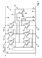
- first embodiment of the inverter 10 includes a switch driver 14 (which is also referred to as control electronics 14) and for each of the winding strands i each have an upper-side switch (flow control valve ) S iH and a respective lower-side switch S iL .
- the index i can take the values U, V, W and the index j the values H and L.
- the switches S ij can be provided by alternately connecting to a positive 16 and a negative 18 poled power supply line on the connecting lines K i for each of the strands i with respect to the negative-polarity supply line 18 depending on an AC voltage U i .
- each of the connection lines K i can be switched to each of the following three states.
- the switch pair S UH , S UL or S VH , S VL or S WH , S WL which leads to the respective connecting line K i , high impedance, ie it is in the main flow direction 19 of the voltage source 28 is not a connection to the positive 16 still to the negative supply line 18.
- the respective switch S iH connects to the positive supply line 16.
- the respective switch S iL connects to the negative supply line 18. Die Fig.
- the switch S ij each of which has a controllable semiconductor Q ij , each with a freewheeling diode D ij .
- the controllable semiconductor Q ij is typically an IGBT (insulated gate bipolar transistor) or MOSFET (metal oxide semiconductor field effect transistor).
- the switches S ij can each be provided with a freewheeling diode D ij connected in parallel.
- the free-wheeling diode D ij is not shown separately, as it (other than an IGBT) is not present here as a separate component, but as a parasitic or integrated component of the controllable semiconductor Q ij , which may be for example a MOSFET ,
- electromechanical actuators such as electromechanical steering and electric brakes
- operating conditions such as “hold at the end stop” or “tension with maximum force” occur in which the associated electric motor 12 is operated with respect to its nominal sizes at low rotational speed or even standstill with a high torque becomes.
- conventional modulation in the most problematic motor positions at least one of the switches S ij in a range of 360 ° divided by the number n of the phases continuously conductive.
- conventional inverters are dimensioned such that all switches S ij of the half bridges can carry the entire phase current I i permanently.
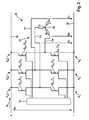
- Fig. 3 shows for a first drive state t 1, an equivalent circuit diagram of the inverter 10 with the connected three-phase machine 12, which is at a standstill.
- R Li represents the strand resistance and L i the inductance of the respective strand.
- S ij represents the actual switching function (without ohmic losses) and R Sij the ohmic resistance of the switch S ij .
- R Sij is for example about 20 m ⁇ , R Li about 200 m ⁇ and the supply voltage Up about 10 V.
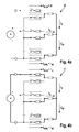
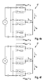
- Fig. 4b and Fig. 4f show the same drive state t 1 in a more schematic form.
- Another drive state t 2 of the total of six possible drive states t 1 to t 6 is in the Fig. 4c and 4e played.
- Fig. 4a and 4d show freewheeling states t 0 , t 7 , in which the voltage source 28 is disconnected.
- the switches S ij are typically switched so that none of the drive phases t 1 .. t 6 lasts more than a few microseconds.
- the inverter 10 is typically freewheeling for the majority of the time, typically alternating both freewheeling states t 0 , t 7 , to thereby avoid switching losses by switching only one of the branches i at each state change.
- the Fig. 4a to 4f show a typical sequence of switching states t 0 ..T 7 of the inverter 10 over an entire shift sequence period T p.
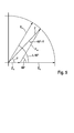
- Fig. 5 shows a section of a space vector diagram for a modulation sector k.
- Each of the elementary space pointers E k and E n represents a direction and magnitude
- Within the modulation sector k can by means of the addition of two partial space vector Z k, n Z, in the direction of the unit space vector E k and E show n, any desired space vector Z with any desired magnitude
- a pulse width modulation is typically used. From the set of sines and the angle of rotation theorem, it follows that the ratio of the strengths
- the subspace pointer Z k , Z n with t nP / t kP (sin ⁇ ) / sin (60 ° - ⁇ ) (Equation 1) is to be measured.
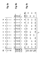
- Fig. 6a explains the example of the Fig. 4a to 4f an inventive modulation method, wherein the drive states t k t n depending on the desired strength
- the total times t 0P .. t 7P of an operating state t 0 ... T 7 related to a switching sequence period T p are identified here by the index P.
- t n is ⁇ according to equation 1 in the example about 19 °.
- the sum column I REL provides information about the resulting from the integration relative height I REL of the DC currents I i in the strands i.
- Fig. 6c gives an overview of the current loads of the switch S ij .
- the sum columns SBH, SBL provide information about the relative total current load SBH, SBL of the individual switches S ij .
- the free-wheeling state t 0 two time slices ZS maintained longer than the freewheeling state t 7 , so as to relieve the switch S UH .
- the heat generation in a switch S ij follows a non-linear, for example quadratic, and not necessarily mirror-symmetric function P (I i ).
- the time division t 0P / t 7P is specifically influenced in order to achieve a more uniform load P (I sij ) of the switches S ij . This was in the example of the Fig.
- m S 3/2 (1 + t 2P - t 1P - (t 0P - t 7P )).
- the modulation degree offset m C to be applied is the difference of m S less a sum modulation degree m S0 applied by the switch driver 14, 32 without regard to the stress distribution.
- Such a modulation degree offset m C which is added to all modulation levels m U , m V , m W , causes modulation patterns with optimum time division t 0P / t 7P of the freewheeling phases t 0 , t 7 to be generated by means of conventional subsequent steps.
- the modulation degree offset m C can be applied continuously or in blocks. In both variants, a negative modulation degree offset m C is possible.
- the time length of the time blocks for manipulation of the modulation degree offset m C should not be greater than a shortest load-relevant thermal time constant T th of the inverter, which is typically in the range between 0.1 ms and 100 ms.
- Fig. 7 shows an arrangement for the switch driver 14 for a time division t 0P / t 7P of the two freewheeling states t 0 and t 7 for the purpose of load distribution.
- the arrangement comprises a conventional first switching pattern generator 32, a freewheeling optimizer 33 according to the invention, a conventional pulse width modulator 34 and an armature 10 branch arrangement.
- the first switching pattern generator 32 is designed to provide a sequence of switching signals 36, 37, 38 for activating drive states t 1 ..t 6 or to activate freewheeling states t 0 and t 7 to produce.
- the pulse width modulator 36 is provided to switch from the switching signals 36, 37, 38 pulse width modulated control signals 39 for the switch S ij to produce.
- the freewheel optimizer 34 may be implemented as an optional or retrofittable device or software function.
- a controller 40 of the freewheel optimizer 34 receives the switching signals 36 to activate the drive states t 1 ..t 6 and calculates a time division t 0P / t 7P between the two freewheeling states t 0 , t 7. With this information, the controller 40 generate control signals 42 for a second switching pattern generator 44 which generates modified switching signals 46 for activating the freewheeling states t 0P / t 7P .
- measurement results 48 in particular current, voltage and temperature measured values from a range of the switches S ij and / or the electric machine 12, are included in the calculation of the time division t 0P / t 7P .
- a torque as well as a position and / or an electrical and / or mechanical angle of the electric machine 12 can be detected in order to determine a load state P (I Sij ), in particular a current state I Sij , of the inverter 10 and to close its switch S ij and to optimize a time division t 0P / t 7P between freewheeling states t 0 , t 7 .
- the invention is particularly advantageous for the operation of an inverter 10, in which a total time t 0P + t 7P of the freewheeling states t 0, t 7 is greater than a quarter of a total time t AP of the drive states t 1 ..t 6 , in particular greater as the total time t AP of the drive states t 1 ..t 6 , in particular greater than four times or ten times the total time t AP of the drive states t 1 ..t 6 .
Landscapes
- Engineering & Computer Science (AREA)
- Power Engineering (AREA)
- Inverter Devices (AREA)
Applications Claiming Priority (2)
| Application Number | Priority Date | Filing Date | Title |
|---|---|---|---|
| DE102008054970 | 2008-12-19 | ||
| DE102009002903A DE102009002903A1 (de) | 2008-12-19 | 2009-05-07 | Belastungsverteilung für Wechselrichter |
Publications (2)
| Publication Number | Publication Date |
|---|---|
| EP2200166A2 true EP2200166A2 (fr) | 2010-06-23 |
| EP2200166A3 EP2200166A3 (fr) | 2016-10-12 |
Family
ID=42084615
Family Applications (1)
| Application Number | Title | Priority Date | Filing Date |
|---|---|---|---|
| EP09178467.8A Withdrawn EP2200166A3 (fr) | 2008-12-19 | 2009-12-09 | Répartition de charge dans un onduleur pour réduire sa charge |
Country Status (2)
| Country | Link |
|---|---|
| EP (1) | EP2200166A3 (fr) |
| DE (1) | DE102009002903A1 (fr) |
Families Citing this family (2)
| Publication number | Priority date | Publication date | Assignee | Title |
|---|---|---|---|---|
| DE102012210654A1 (de) * | 2012-06-22 | 2013-12-24 | Robert Bosch Gmbh | Verfahren und Vorrichtung zum Ansteuern eines Wechselrichters |
| DE102012210652A1 (de) | 2012-06-22 | 2013-12-24 | Robert Bosch Gmbh | Verfahren und Vorrichtung zum Ansteuern eines Wechselrichters |
Family Cites Families (4)
| Publication number | Priority date | Publication date | Assignee | Title |
|---|---|---|---|---|
| US4777578A (en) * | 1988-01-04 | 1988-10-11 | General Electric Company | Integrated current sensor torque control for ac motor drives |
| US5285145A (en) * | 1988-08-30 | 1994-02-08 | Fuji Electric Co., Ltd. | Current-limit system for voltage-type inverter |
| US6906481B1 (en) | 2003-12-03 | 2005-06-14 | The Boeing Company | Power sharing high frequency motor drive modular system |
| US7755319B2 (en) * | 2007-05-31 | 2010-07-13 | Gm Global Technology Operations, Inc. | Apparatus, systems, and methods for reducing voltage source inverter losses |
-
2009
- 2009-05-07 DE DE102009002903A patent/DE102009002903A1/de not_active Withdrawn
- 2009-12-09 EP EP09178467.8A patent/EP2200166A3/fr not_active Withdrawn
Also Published As
| Publication number | Publication date |
|---|---|
| EP2200166A3 (fr) | 2016-10-12 |
| DE102009002903A1 (de) | 2010-06-24 |
Similar Documents
| Publication | Publication Date | Title |
|---|---|---|
| DE102008018950B4 (de) | Verfahren und System zur Impulspositionsplanung bei Elektroantrieben | |
| DE112008001796B4 (de) | Wechselrichtersystem und Steuerverfahren | |
| EP2786462B1 (fr) | Procédé de commande d'un convertisseur multiphase | |
| DE102015214768A1 (de) | Steuervorrichtung für eine rotationsmaschine | |
| DE1920351A1 (de) | Elektrischer Schrittschaltmotor | |
| EP2596577B1 (fr) | Procédé et dispositif de commande d'une machine électrique polyphasée, et système moteur | |
| DE102007036023B4 (de) | Verfahren und Vorrichtung für PWM-Steuerung eines Spannungsquellen-Wechselrichters zum Minimieren von Stromabtastfehlern bei elektrischen Antrieben | |
| WO2012122978A2 (fr) | Convertisseur pour un moteur électrique et procédé de commande d'un disjoncteur | |
| EP2730021B1 (fr) | Procédé de commande d'une machine polyphasée | |
| DE112020006566T5 (de) | Stromrichtereinrichtung | |
| DE112018000320T5 (de) | Antriebsvorrichtung | |
| DE112020006514T5 (de) | Stromrichtereinrichtung und motorsystem | |
| WO2019192770A1 (fr) | Commande d'entraînement pour un moteur triphasé | |
| DE202019005419U1 (de) | Steuerung für elektrische Servolenkungsteuerung für elektrische Servolenkung | |
| EP0505591B1 (fr) | Méthode et dispositif pour la régulation d'un vecteur bidimensionnel d'une charge en utilisant un contrôleur digital avec une fréquence de commutation limitée | |
| DE102009002903A1 (de) | Belastungsverteilung für Wechselrichter | |
| WO2017032787A1 (fr) | Procédé de détermination d'un angle de précommutation d'une machine électrique | |
| WO2013092039A1 (fr) | Montage de convertisseur | |
| EP3853058A1 (fr) | Dispositif de commande conçu pour un onduleur, onduleur conçu pour un véhicule, véhicule et procédé pour faire fonctionner un onduleur | |
| DE112023001779T5 (de) | Linearmotor-Antriebseinrichtung und Linearmotor | |
| DE102012210664A1 (de) | Verfahren und Vorrichtung zum Ansteuern eines Wechselrichters | |
| EP2928055B1 (fr) | Convertisseur de courant modulaire et procédé de production d'une tension de sortie sinusoïdale à harmoniques réduites | |
| DE102019207756A1 (de) | Betreiben von Schaltelementen eines Wechselrichters | |
| DE102012210663A1 (de) | Verfahren und Vorrichtung zum Ansteuern eines Wechselrichters | |
| EP1293033B1 (fr) | Commande et regulation de moteurs electriques |
Legal Events
| Date | Code | Title | Description |
|---|---|---|---|
| PUAI | Public reference made under article 153(3) epc to a published international application that has entered the european phase |
Free format text: ORIGINAL CODE: 0009012 |
|
| AK | Designated contracting states |
Kind code of ref document: A2 Designated state(s): AT BE BG CH CY CZ DE DK EE ES FI FR GB GR HR HU IE IS IT LI LT LU LV MC MK MT NL NO PL PT RO SE SI SK SM TR |
|
| PUAL | Search report despatched |
Free format text: ORIGINAL CODE: 0009013 |
|
| RIC1 | Information provided on ipc code assigned before grant |
Ipc: H02M 7/5387 20070101ALI20160831BHEP Ipc: H02M 7/48 20070101ALI20160831BHEP Ipc: H02M 7/219 20060101ALI20160831BHEP Ipc: H02M 7/217 20060101AFI20160831BHEP |
|
| AK | Designated contracting states |
Kind code of ref document: A3 Designated state(s): AT BE BG CH CY CZ DE DK EE ES FI FR GB GR HR HU IE IS IT LI LT LU LV MC MK MT NL NO PL PT RO SE SI SK SM TR |
|
| 17P | Request for examination filed |
Effective date: 20170412 |
|
| RBV | Designated contracting states (corrected) |
Designated state(s): AT BE BG CH CY CZ DE DK EE ES FI FR GB GR HR HU IE IS IT LI LT LU LV MC MK MT NL NO PL PT RO SE SI SK SM TR |
|
| STAA | Information on the status of an ep patent application or granted ep patent |
Free format text: STATUS: THE APPLICATION IS DEEMED TO BE WITHDRAWN |
|
| 18D | Application deemed to be withdrawn |
Effective date: 20170413 |