EP2199954A1 - Halbleiterspeicheranordnung und speichersystem - Google Patents
Halbleiterspeicheranordnung und speichersystem Download PDFInfo
- Publication number
- EP2199954A1 EP2199954A1 EP08835488A EP08835488A EP2199954A1 EP 2199954 A1 EP2199954 A1 EP 2199954A1 EP 08835488 A EP08835488 A EP 08835488A EP 08835488 A EP08835488 A EP 08835488A EP 2199954 A1 EP2199954 A1 EP 2199954A1
- Authority
- EP
- European Patent Office
- Prior art keywords
- semiconductor storage
- unit
- data
- storage device
- electric power
- Prior art date
- Legal status (The legal status is an assumption and is not a legal conclusion. Google has not performed a legal analysis and makes no representation as to the accuracy of the status listed.)
- Granted
Links
Images


Classifications
-
- G—PHYSICS
- G11—INFORMATION STORAGE
- G11C—STATIC STORES
- G11C17/00—Read-only memories programmable only once; Semi-permanent stores, e.g. manually-replaceable information cards
- G11C17/08—Read-only memories programmable only once; Semi-permanent stores, e.g. manually-replaceable information cards using semiconductor devices, e.g. bipolar elements
- G11C17/10—Read-only memories programmable only once; Semi-permanent stores, e.g. manually-replaceable information cards using semiconductor devices, e.g. bipolar elements in which contents are determined during manufacturing by a predetermined arrangement of coupling elements, e.g. mask-programmable ROM
-
- G—PHYSICS
- G11—INFORMATION STORAGE
- G11C—STATIC STORES
- G11C5/00—Details of stores covered by group G11C11/00
- G11C5/02—Disposition of storage elements, e.g. in the form of a matrix array
- G11C5/04—Supports for storage elements, e.g. memory modules; Mounting or fixing of storage elements on such supports
-
- G—PHYSICS
- G11—INFORMATION STORAGE
- G11C—STATIC STORES
- G11C7/00—Arrangements for writing information into, or reading information out from, a digital store
- G11C7/10—Input/output [I/O] data interface arrangements, e.g. I/O data control circuits, I/O data buffers
- G11C7/1006—Data managing, e.g. manipulating data before writing or reading out, data bus switches or control circuits therefor
-
- H—ELECTRICITY
- H10—SEMICONDUCTOR DEVICES; ELECTRIC SOLID-STATE DEVICES NOT OTHERWISE PROVIDED FOR
- H10F—INORGANIC SEMICONDUCTOR DEVICES SENSITIVE TO INFRARED RADIATION, LIGHT, ELECTROMAGNETIC RADIATION OF SHORTER WAVELENGTH OR CORPUSCULAR RADIATION
- H10F19/00—Integrated devices, or assemblies of multiple devices, comprising at least one photovoltaic cell covered by group H10F10/00, e.g. photovoltaic modules
- H10F19/30—Integrated devices, or assemblies of multiple devices, comprising at least one photovoltaic cell covered by group H10F10/00, e.g. photovoltaic modules comprising thin-film photovoltaic cells
-
- H—ELECTRICITY
- H10—SEMICONDUCTOR DEVICES; ELECTRIC SOLID-STATE DEVICES NOT OTHERWISE PROVIDED FOR
- H10F—INORGANIC SEMICONDUCTOR DEVICES SENSITIVE TO INFRARED RADIATION, LIGHT, ELECTROMAGNETIC RADIATION OF SHORTER WAVELENGTH OR CORPUSCULAR RADIATION
- H10F19/00—Integrated devices, or assemblies of multiple devices, comprising at least one photovoltaic cell covered by group H10F10/00, e.g. photovoltaic modules
- H10F19/80—Encapsulations or containers for integrated devices, or assemblies of multiple devices, having photovoltaic cells
-
- H—ELECTRICITY
- H10—SEMICONDUCTOR DEVICES; ELECTRIC SOLID-STATE DEVICES NOT OTHERWISE PROVIDED FOR
- H10F—INORGANIC SEMICONDUCTOR DEVICES SENSITIVE TO INFRARED RADIATION, LIGHT, ELECTROMAGNETIC RADIATION OF SHORTER WAVELENGTH OR CORPUSCULAR RADIATION
- H10F77/00—Constructional details of devices covered by this subclass
- H10F77/10—Semiconductor bodies
- H10F77/16—Material structures, e.g. crystalline structures, film structures or crystal plane orientations
- H10F77/169—Thin semiconductor films on metallic or insulating substrates
- H10F77/1692—Thin semiconductor films on metallic or insulating substrates the films including only Group IV materials
-
- H10W72/00—
-
- H10W90/293—
-
- G—PHYSICS
- G11—INFORMATION STORAGE
- G11C—STATIC STORES
- G11C2207/00—Indexing scheme relating to arrangements for writing information into, or reading information out from, a digital store
- G11C2207/10—Aspects relating to interfaces of memory device to external buses
- G11C2207/107—Serial-parallel conversion of data or prefetch
-
- H10W90/00—
-
- Y—GENERAL TAGGING OF NEW TECHNOLOGICAL DEVELOPMENTS; GENERAL TAGGING OF CROSS-SECTIONAL TECHNOLOGIES SPANNING OVER SEVERAL SECTIONS OF THE IPC; TECHNICAL SUBJECTS COVERED BY FORMER USPC CROSS-REFERENCE ART COLLECTIONS [XRACs] AND DIGESTS
- Y02—TECHNOLOGIES OR APPLICATIONS FOR MITIGATION OR ADAPTATION AGAINST CLIMATE CHANGE
- Y02E—REDUCTION OF GREENHOUSE GAS [GHG] EMISSIONS, RELATED TO ENERGY GENERATION, TRANSMISSION OR DISTRIBUTION
- Y02E10/00—Energy generation through renewable energy sources
- Y02E10/50—Photovoltaic [PV] energy
Definitions
- the present invention relates to a semiconductor storage device using a semiconductor device as well as a storage system including it, and particularly to a technique that can reliably perform long-term data storage.
- such a form is expected that edition is performed after digitizing the image in the image-taking process, and screening is performed by distributing it to movie theaters over a network.
- the use of such digital data can prevent deterioration of images that may occur due to age deterioration of films and mechanical damages caused by screening.
- the digital information is stored by storing them on various recording mediums such as magnetic tape, magnetic disc, optical disc, magneto-optical disc or flash memory.
- these recording mediums have a limited life.
- the optical discs such as CD (Compact Disc) and DVD (Digital Versatile Disc) have the life of several tens of years because a recording layer made of aluminum or the like corrodes due to intrusion of atmosphere.
- the recording medium such as magnetic tape or magnetic disc (e.g., hard disc or flexible disc) of the type that records data using the magnetism
- the magnetism itself naturally decays with time, and further is liable to be affected by external magnetic field so that it is practically difficult to keep the data storage for a long term.
- the recording medium such as a flash memory of the type that uses electric charges for storing the data, the charges themselves naturally decay with time and are liable to be affected by external magnetic field so that it is practically difficult to keep the data storage for a long term.
- Patent Document 1 Japanese Patent Laying-Open No. 2006-237454 has disclosed a structure and a manufacturing method of the above mask ROM.
- the semiconductor storage device described above has an electric circuit formed of silicon layers containing a small amount of impurities, a metal layer and others, and stores information (digital data) by bringing the information into correspondence with a quantity of a current flowing in this electric circuit and/or presence/absence of such a current.
- the reading of information from the semiconductor storage device means outputting of an electric signal corresponding to the stored information from the semiconductor storage device. Therefore, the semiconductor storage device is provided with an input/output unit made of metal and called a "pad unit" as an interface for reading the information.
- an ordinary pad unit is exposed to an atmosphere so that circuits formed in the semiconductor storage device may be corroded through the pad unit. Further, even when the corrosion can be suppressed by filling resin into the pad unit, or by keeping and managing it in an inert gas or under a vacuum condition, problems of corrosion and abrasion may occur on a metal terminal that is in contact with the pad unit for reading out the information. Thus, the problems of corrosion and abrasion cannot be avoided as long as the contact type is used for implementing the information reading. For these reasons, it is difficult to store the information permanently in the semiconductor storage device.
- the invention has been made for overcoming the above problems, and an object of the invention is to provide a semiconductor storage device that has a longer life than the conventional semiconductor storage device as well as a storage system including the semiconductor storage device.
- a semiconductor storage device includes a substrate; a nonvolatile storage unit arranged on the substrate for nonvolatilely storing data; an electric power generating unit arranged on the substrate for receiving energy externally supplied in a non-contact fashion and generating internal electric power; a transmitting unit arranged on the substrate for receiving the internal electric power and transmitting by radio the data stored in the nonvolatile storage unit; and a sealing film covering exposed surfaces of the nonvolatile storage unit, the electric power generating unit and the transmitting unit.
- the substrate is a glass substrate
- the electric power generating unit is a solar cell configured to receive light passed through the glass substrate.
- the semiconductor storage device further includes an antenna connected to the transmitting unit.
- the electric power generating unit extracts a part of radio signals received through the antenna as electric power.
- the semiconductor storage device includes a plurality of storage cells separated from each other.
- Each of the plurality of storage cells includes the nonvolatile storage unit, the electric power generating unit and the transmitting unit, and a frequency of the radio signal transmitted from the transmitting unit of each of the storage cells is different from those of the other cells.
- the sealing film is a silicon dioxide film.
- a storage system includes a semiconductor storage device; and a data reading device.
- the semiconductor storage device includes a substrate, a plurality of storage cells arranged on the substrate, and a sealing film covering exposed surfaces of the plurality of storage cells.
- Each of the plurality of storage cells includes a nonvolatile storage unit for nonvolatilely storing data, an electric power generating unit for receiving energy externally supplied in a non-contact fashion and generating internal electric power, and a transmitting unit for receiving the internal electric power and transmitting by radio the data stored in the nonvolatile storage unit.
- the data reading device includes an energy supply unit for supplying energy to the semiconductor storage device, and a plurality of receiving units arranged corresponding to the plurality of storage cells of the semiconductor storage device, respectively.
- a storage system includes a plurality of semiconductor storage devices; and a data reading device.
- the plurality of semiconductor storage devices are arranged close according to a predetermined rule.
- Each of the plurality of semiconductor storage devices includes a light-transmitting substrate; an electric power generating unit for receiving the light passed through the substrate and generating electric power, a nonvolatile storage unit arranged on the substrate for nonvolatilely storing the data, a communication unit arranged on the substrate for receiving the electric power from the electric power generating unit and transmitting by radio the data stored in the nonvolatile storage unit to the semiconductor storage device neighboring to the device to which the communication unit belongs, and a sealing film covering exposed surfaces of the electric power generating unit, the nonvolatile storage unit and the communication unit.
- the data reading device includes a light emitting unit for emitting light to the plurality of semiconductor storage devices, and a reading unit arranged close to at least one of the plurality of closely arranged semiconductor storage devices for receiving the data transmitted by radio from the semiconductor storage device.
- the communication unit transfers the data received from any neighboring semiconductor storage device to any other semiconductor memory device of the semiconductor storage devices.
- the communication unit transfers the data received from the neighboring semiconductor storage device to a destination and thereafter transmits the data stored in the nonvolatile storage device to the destination.
- the substrate has a substantially circular disk-like form.
- the communication unit includes a receiving unit for receiving the data from a semiconductor storage devices neighboring to the device to which the communication unit belongs, and a transmitting unit for transmitting the data to another semiconductor storage devices neighboring to the device to which the communication unit belongs.
- the receiving unit and the transmitting unit are spaced from each other by a predetermined circumferential angle about a center of the substantially circular disk-like substrate.
- the plurality of semiconductor storage devices are arranged to have diametrical centers aligned on the same straight line, and the receiving unit of one of the neighboring two semiconductor storage devices is close to the transmitting unit of the other of the neighboring two semiconductor storage devices.
- each of the plurality of semiconductor storage devices is arranged such that it is close to the semiconductor storage devices.
- the communication unit includes a plurality of transmitting/receiving units configured to perform data transmission and data reception with respect to the semiconductor storage device neighboring to the device to which the communication unit belongs.
- Each of the transmitting/receiving units establishes an ad-hoc network with respect to the neighboring semiconductor storage device.
- the sealing film is a silicon dioxide film.
- the invention provides a semiconductor storage device for use in a storage system including a plurality of semiconductor storage devices arranged close to each other according to a predetermined rule.
- the semiconductor memory device includes a light-transmitting substrate; an electric power generating unit for receiving the light passed through the substrate and generating electric power; a nonvolatile storage unit arranged on the substrate for nonvolatilely storing the data; a communication unit arranged on the substrate for receiving the electric power from the electric power generating unit and transmitting by radio the data stored in the nonvolatile storage unit to the semiconductor storage device neighboring to the device to which the communication unit belongs; and a sealing film covering exposed surfaces of the electric power generating unit, the nonvolatile storage unit and the communication unit.
- a storage system includes a plurality of semiconductor storage devices; and a data reading device.
- the plurality of semiconductor storage devices are arranged close according to a predetermined rule.
- Each of the plurality of semiconductor storage devices includes a substrate, a nonvolatile storage unit arranged on the substrate for nonvolatilely storing the data, an electric power generating unit arranged on the substrate for receiving energy externally supplied in a non-contact fashion and generating internal electric power, a communication unit arranged on the substrate and being configured to receive the internal electric power and perform transmission and reception of the data by radio signals with respect to the semiconductor storage device neighboring to the device to which the communication unit belongs, and a sealing film covering exposed surfaces of the electric power generating unit, the nonvolatile storage unit and the communication unit.
- the communication unit When the communication unit receives the data from any neighboring semiconductor storage device, the communication unit transfers the received data to any other semiconductor memory device.
- the data reading device includes a reading unit neighboring to at least one of the plurality of closely arranged semiconductor storage devices for receiving the data transferred from the neighboring semiconductor storage device.
- the communication unit transfers the data received from the neighboring semiconductor storage device to a destination and thereafter transmits the data stored in the nonvolatile storage device to the destination.
- each of the plurality of semiconductor storage devices is arranged close to the semiconductor storage devices.
- the communication unit includes a plurality of transmitting/receiving units configured to perform data transmission and data reception with respect to the semiconductor storage device neighboring to the device to which the communication unite belongs.
- Each of the transmitting/receiving units establishes an ad-hoc network with respect to the neighboring semiconductor storage device.
- the substrate is a light-transmitting substrate
- the electric power generating unit is a solar cell for receiving light passed through the substrate and generating an electric power
- the data reading device further includes a light for emitting unit emitting the light to the plurality of semiconductor storage devices.
- the data reading device further includes a magnetic flux supply unit for supplying an alternating magnetic flux to the plurality of semiconductor storage devices
- the electric power generating unit includes a coil disposed in a position causing linkage with the alternating magnetic flux, and a power supply circuit for producing the internal electric power from electromotive force generated by linkage between the coil and the alternating magnetic flux.
- the invention provides a semiconductor storage device for use in a storage system formed of a plurality of semiconductor storage devices arranged close to each other according to a predetermined rule.
- the semiconductor memory device includes a substrate; a nonvolatile storage unit arranged on the substrate for nonvolatilely storing data; an electric power generating unit arranged on the substrate for receiving energy externally supplied in a non-contact fashion and generating internal electric power; a communication unit arranged on the substrate and being configured to receive the internal electric power and perform transmission and reception of the data by radio signals with respect to the semiconductor storage device neighboring to the device to which the communication unit belongs; and a sealing film covering exposed surfaces of the electric power generating unit, the nonvolatile storage unit and the communication unit.
- the communication unit transfers the received data to any other neighboring semiconductor memory device.
- the invention can provide the semiconductor storage device that has a longer life than the conventional semiconductor storage device as well as the storage system including the semiconductor storage device.
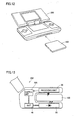
- Fig. 1 shows an outer appearance of a storage system 300 according to a first embodiment of the invention.
- storage system 300 functions as a kind of data accumulation device. Specifically, storage system 300 is provided at its side surface with a plurality of insertion openings 3001 for accepting a plurality of semiconductor storage devices 100. Storage system 300 reads necessary information from these semiconductor storage devices 100 and provides it to external devices (not shown). The number of semiconductor storage devices 100 that storage system 300 can accept is appropriately designed according to a required speed in each data read operation and/or a quantity of data to be accumulated.
- semiconductor storage device 100 is used as a storage medium for storing data that is valuable as cultural properties such as pictorial arts and movies. Since any semiconductor storage device 100 can be inserted into storage system 300, storage system 300 may be configured such that only required devices 100 selected from among many semiconductor storage devices 100 are inserted into it.
- the data read from each of semiconductor storage devices 100 inserted into storage system 300 is transferred toward storage system 300 by radio signals.
- Fig. 2 schematically shows a typical sectional structure of storage system 300 shown in Fig. 1 .
- Fig. 2 shows a structure having only three insertion openings.
- an appropriate structure corresponding to the number of the insertion openings are practically employed.
- storage system 300 includes a control unit 10, a plurality of light emitting units 20, a plurality of receiving units 30 and an interface unit 12.
- Storage system 300 is provided at its side portion with the plurality of insertion openings for accepting semiconductor storage devices 100.
- Light emitting unit 20 and light receiving unit 30 are arranged on the upper and lower sides of each insertion opening, respectively.
- Each light emitting unit 20 is an energy supply unit that supplies the energy to corresponding semiconductor storage device 100 in a non-contact fashion, and typically includes a light source such as an LED (Light Emitting Diode). More specifically, each light emitting unit 20 receives the electric power from the power supply unit (not shown) to generate the light, and emits the generated light toward semiconductor storage device 100 from the lower side on the sheet of the figure. Each receiving unit 30 receives the data that is transmitted from corresponding semiconductor storage device 100 receiving the light emitted from light emitting unit 20, and provides the received data to control unit 10. Control unit 10 includes a CPU and a RAM (Random Access Memory), receives the data provided from each receiving unit 30 and performs predetermined processing.
- a light source such as an LED (Light Emitting Diode). More specifically, each light emitting unit 20 receives the electric power from the power supply unit (not shown) to generate the light, and emits the generated light toward semiconductor storage device 100 from the lower side on the sheet of the figure.
- Each receiving unit 30 receives the
- Interface unit 12 is a portion for providing to an external device (not shown) read data that is produced after it undergoes predetermined processing by control unit 10, and typically is a wired interface such as Ethernet (registered trademark), USB (Universal Serial Bus), IEEE (Institute of Electrical and Electronic Engineers) 1394, SCII (Small Computer System Interface) or RS-232C, or a wireless interface such as a wireless LAN (Local Area Network) or Bluetooth (registered trademark).
- Ethernet registered trademark
- USB Universal Serial Bus
- IEEE Institute of Electrical and Electronic Engineers 1394
- SCII Small Computer System Interface
- RS-232C Serial Bus
- a wireless interface such as a wireless LAN (Local Area Network) or Bluetooth (registered trademark).
- Fig. 3 schematically shows semiconductor storage device 100 according to the first embodiment of the invention.
- semiconductor storage device 100 includes a plurality of storage cells 120 that are formed on a substrate 102 and are separated from each other.
- Substrate 102 is made of a physicochemically stable insulating substance such as silicon or glass. In an example of the structure of the present embodiment, it is made of light-transmitting glass. Further, exposed surfaces of the plurality of storage cells 120 are entirely covered with a sealing film, which is typically made of a physicochemically stable insulating substance such as a film of silicon dioxide.
- Each storage cell 120 has stored the data in advance. As will be described later, each storage cell 120 receives energy from a portion outside semiconductor storage device 100 in a non-contact manner, and successively transmits (responds) the stored data as radio signals.
- Fig. 3 schematically shows the plurality of storage cells 120 separated from each other. However, the structure in which storage cells 120 are clearly separated is not essential.
- Fig. 4 is a block diagram showing functional structures of semiconductor storage device 100 and receiving unit 30 according to the first embodiment of the invention.
- each of storage cells 120 forming semiconductor storage device 100 includes a solar cell 50, a control circuit 60, a mask ROM 70, a transmitting circuit 80 and an antenna 90.
- Solar cell 50 is formed on substrate 102 ( Fig. 3 ) side, and generates internal power by receiving the light that is emitted from light emitting unit 20 and is passed internally through substrate 102 ( Fig. 3 ). Solar cell 50 supplies the generated internal power to control circuit 60 and transmitting circuit 80.
- control circuit 60 When solar cell 50 starts the supply of the power, control circuit 60 reads the data from mask ROM 70 in a predetermined cycle, and provides it to transmitting circuit 80. Particularly, control circuit 60 includes a counter circuit 601. When counter circuit 601 receives the internal power from solar cell 50, it resets its count and starts the count-up in a predetermined cycle. According to the count thus counted up, control circuit 60 successively designates predetermined addresses in mask ROM 70 to perform the data reading. When all the addresses in mask ROM 70 are read, control circuit 60 repeats the data read operation starting from the first address in mask ROM 70. Thus, control circuit 60 cyclically performs the data reading from mask ROM 70 as long as solar cell 50 supplies the power.
- Mask ROM 70 is a nonvolatile storing unit that is provided with a circuit pattern corresponding to the data to be stored, and thereby can nonvolatilely store the data.
- mask ROM 70 is formed by transferring a circuit pattern, which is prepared in advance corresponding to the data, to the substrate by a stepper or the like..
- Mask ROM 70 may be replaced with a PROM (Programmable Read Only Memory) that can be programmed after pattern forming.
- PROM Program Read Only Memory
- a laser PROM and a fuse-type PROM have been known as the above kind of PROM.
- data can be stored by a circuit that corresponds to required data and is formed by emitting the light from a portion outside semiconductor memory device 100.
- a PROM disclosed, e.g., in International Laying-Open No. 03/025944 brochure may be used.
- Transmitting circuit 80 receives the electric power from solar cell 50 and thereby produces a modulation signal corresponding to the data that is read from mask ROM 70 by control circuit 60. Transmitting circuit 80 excites antenna 90 by this modulation signal.
- antenna 90 is formed of a looped metal wire formed on the substrate, and receives the modulation signal from transmitting circuit 80 for transmitting the radio signal. Since semiconductor storage device 100 according to the present embodiment includes the plurality of storage cells 120, antenna 90 is configured such that carriers of the radio signals transmitted from respective storage cells 120 may have different frequencies so that the radio signals transmitted from respective storage cells 120 can be identified. Specifically, each antenna 90 has an impedance that can be set to an arbitrary value by adjusting a line length, a line width, a distance between neighboring lines and/or the like of the lines forming antenna 90. An appropriate difference may be set between the impedance values of antenna 90, and thereby respective modulation frequencies can be different from each other. Thereby, the frequency of the radio signal transmitted from each storage cell 120 can be identified.
- Receiving unit 30 of storage system 300 includes a plurality of receiving cells 310 corresponding to storage cells 120 in semiconductor storage device 100, respectively. Each receiving cell 310 receives the radio signal transmitted from storage cell 120 corresponding to semiconductor storage device 100, and decodes the radio signal for producing the data and providing it to control unit 10 ( Fig. 2 ).
- Each receiving cell 310 includes an antenna 301 and a receiving circuit 302.
- Antenna 301 is configured to match antenna 90 of the corresponding storage cell 120. Therefore, each antenna 301 can selectively receive the radio signals transmitted from antenna 90 of the corresponding storage cell 120.
- receiving circuit 302 receives only the radio signal having specific frequency.
- Receiving circuit 302 performs predetermined decoding processing on the voltage signal that antenna 301 connected thereto induces by receiving the radio signal.
- Receiving circuit 302 successively outputs the data obtained by this decoding processing. In the following description, the data that is successively output from respective receiving circuits 302 may also be described as "Ch1, Ch2, ⁇ " hereinafter.
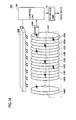
- Fig. 5 schematically shows a sectional structure of semiconductor storage device 100 according to the first embodiment of the invention.
- semiconductor storage device 100 includes a substrate 102, an anti-reflection film 122, an n-type semiconductor layer 124, a p-type semiconductor layer 126, a p+ impurity semiconductor layer 128, an electrode layer 130, through holes 132, 134, 136 and 138, and insulating films 140 and 150.
- n-type semiconductor layer 124 is formed in a predetermined region on substrate 102 that is made of light-transmitting glass primarily made of silicon dioxide.
- N-type semiconductor layer 124 is made of silicon or germanium doped with n-type impurities.
- Anti-reflection film 122 is formed on the lower side of n-type semiconductor layer 124.
- P-type semiconductor layer 126 is formed on the upper side of n-type semiconductor layer 124.
- P+ impurity semiconductor layer 128 is formed on the upper side of p-type semiconductor layer 126.
- n-type, p-type and p+ impurity semiconductor layers 124, 126 and 128 form a solar battery cell of the pn-junction type.
- the light emitted from light emitting unit 20 ( Fig. 2 ) located under semiconductor storage device 100 passes through substrate 102, and then is applied to n-type semiconductor layer 124 through anti-reflection film 122. This light excites electrons in n-type semiconductor layer 124 so that photovoltaic power occurs between n-type and p+ semiconductor layers 124 and 128 according to the quantity of emitted light. This electromotive force supplies the electric power to each circuit.
- Control circuit 60, mask ROM 70, transmitting circuit 80 and antenna 90 are formed on the upper side of the solar cell.
- a part of the power generated in the solar cell is supplied to control circuit 60 via through hole 138 connected to n-type semiconductor layer 124 and via through hole 134 connected to electrode layer 130 arranged on the upper side of p+ impurity semiconductor layer 128.
- a part of the power generated by the solar cell is supplied to transmitting circuit 80 via through hole 136 connected to n-type semiconductor layer 124 and via through hole 132 connected to electrode layer 130.
- An insulating layer 140 is formed between the solar cells of a certain storage cell 120 and the solar cell of neighboring storage cell 120 so that these storage cells are electrically isolated from each other.
- Insulating film 150 is typically made of physicochemically stable glass or silicon dioxide.
- Substrate 102 corresponds to the "substrate”
- mask ROM 70 corresponds to the “nonvolatile storing unit”
- solar cell 50 corresponds to the "electric power generating unit”
- transmitting circuit 80 corresponds to the "transmitting unit”.
- insulating film 150, light emitting unit 20 and receiving unit 30 correspond to the “sealing film”, "energy supply unit” and “receiving unit”, respectively.
- Fig. 6 illustrates an example of the data read from semiconductor storage device 100 according to the first embodiment of the invention.
- counter circuit 601 included in control circuit 60 of storage cell 120 resets its count, and starts an operation of successively reading the data starting from the first address in corresponding mask ROM 70. Consequently, the data starting from the first address of corresponding mask ROM 70 is successively read from each storage cell 120.
- the data is read from next address ADD1, and subsequently the data will be read in a similar manner.
- Fig. 7 is a functional block diagram showing an example of a control structure in receiving unit 30 of storage system 300 according to the first embodiment of the invention.
- a control structure shown in Fig. 7 is employed for reading out the stored data when information (data row) to be stored is assigned to each storage cell 120 of semiconductor storage device 100 according to the order of the address.
- Receiving unit 30 includes functions serving as a parallel-serial converting unit 31, an error correcting circuit 32 and a decoding circuit 33.
- Parallel-serial converting unit 31 serially outputs, as a one-dimensional data, the data row (Ch1, Ch1, ⁇ ) provided in parallel from the respective storage cells 120.
- parallel-serial converting unit 31 outputs the data row in the order of first data of Ch1, first data of Ch2, ⁇ , second data of Ch1, second data of Ch2, ⁇ .
- Error correcting circuit 32 performs predetermined error correction processing on the data column provided from parallel-serial converting unit 31.
- An error correction method called LDPC Low Density Parity Check
- Fig. 8 is a functional block diagram showing another example of the control structure in receiving unit 30 of storage system 300 according to the first embodiment of the invention.
- Receiving unit 30 includes a plurality of buffer units 34 and 36, and a space switch 35.
- Each buffer unit 34 temporarily stores the data that is successively read from the corresponding storage cell 120.
- Space switch 35 selectively extracts the data stored in buffer unit 34 according to the address signal provided from control unit 10 and others, and provides the extracted data to specific buffer unit 36.
- space switch 35 selectively extracts the required data from the data that is read in the order of address from each storage cell 120, and provides it to specific buffer unit 36.
- Buffer unit 36 temporarily stores the data provided from space switch 35, and will output it as the data row when buffer unit 36 has stored a predetermined amount of data. Since the plurality of buffer units are arranged on each of the input and output sides, the data stored in storage cell 120 can be read randomly, and the discretely stored data can be combined to output it as one data row.
- Fig. 9 shows an example of a processing procedure for data flow using semiconductor storage device 100 according to the first embodiment of the invention.
- Fig. 10 shows another example of the processing procedure for data flow using semiconductor storage device 100 according to the first embodiment of the invention.
- Fig. 9 shows a form in which the operations from the start to the data storing are performed under management of a data owner (typically, a copyright holder) in the process of manufacturing semiconductor storage device 100.
- a data owner typically, a copyright holder
- formation of the solar cell on substrate 102 step S101
- formation of each circuit in the layer above the solar cell step S102
- glassivation of portions except for the surfaces of the formed circuits step S103
- the glassivation means the processing of forming a sealing film such as an insulating film. For keeping the state allowing data writing into the mask ROM, the glassivation is not performed on the surfaces of the formed circuits.
- semiconductor storage device 100 After semiconductor storage device 100 is manufactured as described above, pattern formation is performed on the mask ROM according to the data to be stored under the management of the data owner (step S104). Further, the glassivation is performed on the exposed surface of semiconductor storage device 100 (step S105). At this point in time, semiconductor storage device 100 is entirely packaged. Semiconductor storage devices 100 storing the data are distributed to the users.
- Semiconductor storage device 100 distributed to the user is kept in a state where the data can be freely read out by a predetermined data reading device or the like (step S106).
- Fig. 10 shows a form in which the data owner arbitrarily performs the processing of storing the data in semiconductor storage device 100 after the manufacturing of semiconductor storage device 100. Specifically, for manufacturing semiconductor storage device 100, formation of the solar cell on substrate 102 (step S101), formation of each circuit in the layer above the solar cell (step S102) and glassivation of portions except for the surfaces of the formed circuits (step S103) are successively performed. After these steps, semiconductor storage device 100 is supplied to the data owner.
- the data owner performs pattern formation on the mask ROM according to the data to be stored (step S114). Processing the circuit pattern on the mask ROM requires a relatively massive apparatus, it is appropriate that the data owner configures the mask ROM from a laser PROM or fuse-type PROM, and creates the required circuit patter, using laser or the like. When the data owner completes the pattern formation on the mask ROM, the owner then performs the glassivation on the entire surface of semiconductor storage device 100 (step S115). Semiconductor storage devices 100 storing the data are distributed to the users.
- Semiconductor storage device 100 distributed to the user is kept in a state where the data can be freely read out by a predetermined data reading device or the like (step S106).
- the embodiment employs the structure in which the mask ROM for nonvolatilely storing the data and the peripheral circuits for reading the data from the mask ROM are formed on the substrate, and then the exposed surfaces of them are covered with the physicochemically stable sealing film. This can suppress corrosion by the atmosphere, and can implement the data holding for a longer period.
- the circuit structure can be simple.
- the glass substrate having the light-transmitting property the solar cell formed on this substrate can be used to supply the electric power.
- a silicon substrate or the like is electrically conductive to a certain extent, but the glass substrate is a better insulator and therefore has smaller absorptance and higher transmittance of electromagnetic waves so that the glass substrate allows the efficient data communications with smaller transmission power.
- Fig. 11 is a block diagram showing functional structures of a semiconductor storage device 100A and a receiving unit 30A according to a modification of the first embodiment of the invention.
- each storage cell 120A differs from storage cell 120 shown in Fig. 4 in that solar cell 50 is removed, transmitting circuit 80 is replaced with a transmitting/receiving circuit 80A, and control circuit 60 is replaced with a control circuit 60A.
- This storage cell 120A is of the passive type in which when storage cell 120A externally receives a radio signal, the internally stored data responds to it.
- transmitting/receiving circuit 80A receives this radio signal through antenna 90.
- Transmitting/receiving circuit 80A takes out the electric power and identification information from the radio signal provided from receiving cell 310A, and provides it to control circuit 60A.
- Control circuit 60A becomes active in response to reception of the power from receiving cell 310A, and reads the data from the predetermined address in mask ROM 70 according to the input identification information provided from receiving cell 310A. The data thus read is provided to transmitting/receiving circuit 80A.
- Transmitting/receiving circuit 80A uses a part of the radio signal received by antenna 90 to modulate the radio signal with the data read from mask ROM 70, and transmits it.
- Receiving cell 310A includes antenna 301 and a transmitting/receiving circuit 303.
- Transmitting/receiving circuit 303 produces the radio signals for reading the data from storage cell 120A, and transmits it from antenna 301. Also, transmitting/receiving circuit 303 produce the data by decoding the radio signal that is provided from storage cell 120A and received by antenna 301, and outputs it.
- receiving cell 310A performs the data reading from storage cell 120A.
- the radio signal supplies the electric power and the radio signal performs the data reading so that it is possible to apply a design to the surface of semiconductor storage device 100.
- Fig. 12 shows an outer appearance of an example of a structure using a storage system according to a second embodiment of the invention.
- semiconductor storage device 100 according to the second embodiment is used, by way of example, as a recording medium for storing an application executed by a portable game device 200. More specifically, semiconductor storage device 100 nonvolatilely stores program codes to be executed by a processing device such as a CPU (Central Processing Unit) of portable game device 200 as well as various kinds of data.
- Portable game device 200 includes a data reading device for reading the data from semiconductor storage device 100. When semiconductor storage device 100 is inserted into portable game device 200, information is read therefrom.
- CPU Central Processing Unit
- Fig. 13 schematically shows a sectional structure of portable game device 200 shown in Fig. 12 .
- portable game device 200 includes a control unit 10A, light emitting unit 20, receiving unit 30 and a power supply unit (BAT) 40.
- Portable game device 200 is provided on its body side with a recess for inserting semiconductor storage device 100.
- Light emitting unit 20 and receiving unit 30 are arranged on the lower and upper sides of the recess.
- Light emitting unit 20 is an energy supply unit that supplies the energy to semiconductor storage device 100 in a non-contact fashion.
- Light emitting unit 20 generates light from the electric power supplied from power supply unit 40, and emits the generated light from its lower side in the sheet of the figure toward semiconductor storage device 100.
- Receiving unit 30 receives the transmitted data by receiving the light emitted from light emitting unit 20 by semiconductor storage device 100, and provides the received data to control unit 10A.
- Control unit 10A includes a CPU, a RAM, a display circuit and the like, receives the data provided from receiving unit 30 and executes the predetermined processing.
- Power supply unit 40 is typically formed of a storage battery, and supplies drive power to light emitting unit 20 and control unit 10A.
- the present embodiment it is possible to achieve substantially the same effect as that in the first embodiment already described. Also, the data is read in the non-contact fashion from semiconductor storage device 100 so that it is possible to achieve the effect of improving the resistance to mechanical abrasion, chemical rusting and damages due to static electricity. Further, it is possible to achieve the effect of improving the resistance to reverse engineering, modification or the like.
- the circuits are formed on the substrate of a rectangular form that is formed or shaped in advance.
- circuits for implementing the semiconductor storage device according to the invention may be formed on a silicon wafer of a circular disk-like form prepared by crystal growth.
- Fig. 14 shows an outer appearance of a storage system 400 according to a third embodiment of the invention.
- a storage system 400 includes a plurality of semiconductor storage devices 100B, a rack 410 accommodating these semiconductor storage devices 100B, a light emitting unit 20B emitting the light to these semiconductor storage devices 100B, a reading unit 30B arranged close to semiconductor storage device 100B located on one end, a control unit 10B, and interface unit 12.
- Rack 410, light emitting unit 20B, reading unit 30B, control unit 10B and interface unit 12 function as a "data reading device".
- Each of semiconductor storage devices 100B includes a nonvolatile storage unit such as a mask ROM, peripheral circuits performing data reading from the mask ROM and radio transmission thereof, and an electric power generating unit that generates internal electric power by receiving energy supplied from the outside of the battery cell in a non-contact fashion, and these are formed on a silicon wafer of a substantially circular disk-like form.
- Rack 410 accommodates these semiconductor storage devices 100B that are arranged close to each other according to a predetermined rule.
- Semiconductor storage device 100B can typically perform autonomous communications like an ad-hoc network between neighboring semiconductor memory devices 100B.
- each semiconductor storage device 100B transmits by radio the data received from any neighboring semiconductor storage device 100B to any other neighboring, i.e., other semiconductor storage device 100B, and also transmits by radio the data stored in itself to the neighboring semiconductor storage device 100B. Consequently, the data items stored in respective semiconductor storage devices 100B are successively transmitted in a certain direction according to the arrangement rule of semiconductor storage devices 100B.
- the data transmitted from semiconductor storage device 100B located at the downstream end in the above transmission direction is received by reading unit 30B, and is externally output through control unit 10B from interface unit 12.
- semiconductor storage device 100B transmits the data in the autonomous or self-controlled fashion. Therefore, any restriction is imposed in number and order of positions thereof in rack 410, and the addition and exchange of semiconductor storage devices 100B can be easily performed when necessary provided that semiconductor storage devices 100B are arranged close to each other.
- Light emitting unit 20B is substantially the same as light emitting unit 20 except for the light emission area, and therefore description thereof will not be repeated. Since interface unit 12 is already described, description thereof is not repeated.
- Control unit 10B classifies or groups the data items successively transmitted from the plurality of semiconductor storage devices 100B based on the IDs thereof or the like, temporarily accumulates the classified data in the internal memory or the like, and will output the required data from interface unit 12 when it receives an external request.
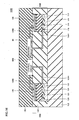
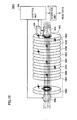
- Fig. 15 is a block diagram showing a planar structure of semiconductor storage device 100B according to the third embodiment of the invention.
- Fig. 16 is a sectional view taken along line XVI - XVI of semiconductor storage device 100B shown in Fig. 15 .
- each semiconductor storage device 100B includes a solar cell 50B, a control circuit 60B, a mask ROM 70B, a transmitting circuit 42 including the antenna for transmission, and a receiving circuit 44 including the antenna for reception.
- Each of transmitting circuit 42 and receiving circuit 44 functions as a "communication unit”.
- Each of these portions and units is formed on the substrate (wafer), and the exposed surfaces thereof are entirely covered with a sealing film (typically, a physicochemically stable insulating substance such as a silicon dioxide film).
- solar cell 50B has a substantially U-shaped or horseshoe-shaped form, is formed on the light-transmitting wafer and generates the internal electric power by receiving the light emitted from light emitting unit 20B ( Fig. 14 ).
- the internally generated power is supplied to control circuit 60B, transmitting circuit 42, receiving circuit 44 and the like.
- Semiconductor storage device 100B according to the present embodiment of the invention is arranged to locate its flat plane close to the planes of different semiconductor storage devices 100B.
- solar cell 50B is formed on the outer periphery side of semiconductor storage device 100B.
- Fig. 15 shows a structure in which solar cell 50B is formed on one surface remote from the surface bearing other circuits.
- solar cells 50B may be formed on the opposite surfaces, respectively, for generating larger internal power.
- control circuit 60B When solar cell 50B starts the power supply, control circuit 60B cooperates with transmitting circuit 42 and receiving circuit 44 to form the ad-hoc network with respect to other semiconductor storage devices 100B. Specifically, when receiving circuit 44 receives the data transmitted from any neighboring semiconductor storage device 100B, control circuit 60B transmits this data received from transmitting circuit 42 to any other neighboring semiconductor storage device 100B. Thus, control circuit 60B functions as a relay device transmitting the data from semiconductor storage device 100B neighboring to itself to other neighboring semiconductor storage device 100B. In addition to this relay operation, control circuit 60B reads the data from mask ROM 70B and provides it to transmitting circuit 42 so that semiconductor storage device 100 transmits the data stored in itself to other semiconductor storage device 100B. More specific communication processing will be described later in detail.
- mask ROM 70B has substantially the same structure as mask ROM 70 already described, description thereof is not repeated.
- Transmitting circuit 42 receives the power from solar cell 50B, and control circuit 60B produces the modulation signal according to the data read from mask ROM 70B. Transmitting circuit 42 excites the antenna (not shown) by this modulation signal, and thereby transmits the radio signal (modulation signal) to a neighboring semiconductor storage device 100B.
- receiving circuit 44 receiving the power from solar cell 50B receives the radio signal form another semiconductor storage device 100B through the antenna (not shown), it decodes the radio signal into data, and provides it to control circuit 60B.
- transmitting circuit 42 and receiving circuit 44 are spaced by a predetermined distance on the wafer surface for preventing interference between the radio signals thereof.
- semiconductor storage device 100B has substantially the same sectional structure as semiconductor storage device 100 according to the first embodiment shown in Fig. 5 , and is formed of substrate 102, anti-reflection film 122, n-type semiconductor layer 124, p-type semiconductor layer 126, p+ impurity semiconductor layer 128, electrode layer 130, through holes 136B and 138B, and insulating films 140 and 150.
- solar cell 50B is formed on a predetermined region of substrate 102 mode of light-transmitting glass that is primarily made of silicon dioxide.
- n-type semiconductor layer 124, p-type semiconductor layer 126 and p+ impurity semiconductor layer 128 form the solar battery cell of the pn-junction type.
- the light emitted from light emitting unit 20B ( Fig. 15 ) is passed through substrate 102, and is emitted through anti-reflection film 122 to n-type semiconductor layer 124.
- This light excites the electrons in n-type semiconductor layer 124, so that an electromotive force occurs between n-type semiconductor layer 124 and p+ semiconductor layer 128 according to the quantity of emitted light.
- This electromotive force supplies the electric power via through holes 136B and 138B to control circuit 60B, receiving circuit 44 and transmitting circuit 42 ( Fig. 15 ).
- solar cell 50B is formed in the region surrounded by substrate 102 and insulating film 140, and insulating film 150 sealingly covers the exposed surfaces of control circuit 60B and others formed on the upper surface of insulating film 140. Therefore, the surface of semiconductor storage device 100B is entirely covered with insulating film 150 of the physicochemically stable glass or silicon dioxide to prevent entry of the atmosphere.
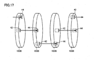
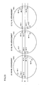
- Fig. 17 schematically shows a state of data transfer in storage system 400 according to the third embodiment of the invention.
- each semiconductor storage device 100B has transmitting circuit 42 and receiving circuit 44 that are formed on the same circular surface and are spaced from each other by a predetermined circumferential angle.
- neighboring semiconductor storage devices 100B are angularly shifted by the above predetermined circumferential angle from each other so that transmitting circuit 42 and receiving circuit 44 formed in one and the other of neighboring semiconductor storage devices 100B, respectively, can be adjacent to each other.
- Fig. 17 shows the case where semiconductor storage devices 100B are successively arranged to keep a positional relationship in which neighboring semiconductor storage devices 100B are angularly and relatively shifted by 90 degrees from each other.
- the ad-hoc network can be formed by the plurality of semiconductor storage devices 100B that are arranged to provide the positional relationship shown in Fig. 17 .
- the data is transmitted unidirectionally from semiconductor storage device 100B on the left side of the sheet of Fig. 17 toward that on the right side of the sheet.
- each semiconductor storage device 100B transmitting circuit 42 and receiving circuit 44 are spaced by a predetermined distance from each other for preventing interference between the received or transmitted radio signals. Further, the intensity of the radio signal transmitted from each transmitting circuit 42 is set so that only nearest receiving circuit 44 can receive it. Thus, the intensity is set such that the radio signal transmitted from certain transmitting circuit 42 to neighboring semiconductor memory device 100B may not affect receiving circuit 44 of another semiconductor memory device 100B.
- Fig. 17 typically shows the example of the structure in which transmitting and receiving circuits 42 and 44 are circumferentially spaced by 90 degrees.
- this circumferential angle is not restricted to it provided the above conditions are satisfied.
- each semiconductor storage device 100B is provided with a recess 110 ( Fig. 15 ) for specifying the relative positional relationship so that the above positioning may be performed easily.
- a projection engageable with recess 110 is formed in an appropriate position. This structure can implement the positional relationship that ensures the radio communications between neighboring semiconductor storage devices 100B.
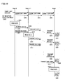
- a topology of the ad-hoc network of storage system 400 shown in Fig. 17 is one-dimensional. Therefore, storage system 400 according to the present embodiment is configured as follows. Storage system 400 transmits the data only in one direction. Also, each semiconductor storage device 100B that is present downstream from certain semiconductor storage device 100B transmits the data received from the upstream side to the downstream side with priority, and will transmit the data stored in itself after the completion of the above received data. A communication sequence relating to this data transmission will be described with reference to Fig. 18 .
- Fig. 18 shows the communication sequence in storage system 400 according to the third embodiment of the invention.
- semiconductor memory devices 100B of N in number are arranged, and are referred to as Node 1, ⁇ Node N-1 and Node N in the order of arrangement from the side near reading unit 20B ( Fig. 15 ) to the other side.
- each semiconductor storage device 100B is activated to start the processing.
- semiconductor storage device 100B located in the upstream end is determined or specified based on whether semiconductor storage device 100B receives a "start signal" from another semiconductor storage device 100B or not.
- a non-receiving state in which the "start signal" is not received from another semiconductor storage device 100B continues in certain semiconductor storage device 100B for a predetermined period after the start of light emission, semiconductor storage device 100B determines that semiconductor storage device 100B itself is located in the upstream end, and transmits the data stored in itself to downstream semiconductor storage device 100B.
- semiconductor storage device 100B itself subsequently transmits the "end signal” to semiconductor storage device 100B on the downstream side.
- semiconductor storage device 100B itself receives the "start signal” from another semiconductor storage device 100B within a predetermined period after the start of the light emission, it determines that another semiconductor storage device 100B is present on the upstream side. Thereby, until semiconductor storage device 100B receives an "end signal” from another semiconductor storage device 100B, semiconductor storage device 100B itself successively transfers the data received from the upstream side to semiconductor storage device 100B on the downstream side.
- semiconductor storage device 100B itself transmits the data stored in itself to downstream semiconductor storage device 100B.
- semiconductor storage device 100B itself subsequently transmits the "end signal” to downstream semiconductor storage device 100B.
- the data is successively transferred from semiconductor storage device 100B in the upstream end toward semiconductor storage device 100B on the downstream side so that it is possible to read the data stored in all semiconductor storage devices 100B of storage system 400.
- each semiconductor storage device 100B when each semiconductor storage device 100B starts the processing, it first transmits the start signal (step S200), and will wait for the reception of the start signal from upstream semiconductor storage device 100B for a predetermined period.
- This predetermined period may be determined randomly.
- At least semiconductor storage device 100B located in the upstream end (i.e., remotest from reading unit 30B ( Fig. 15 )) continues the non-reception state in which it does not receive the start signal from another semiconductor storage device 100B, for a predetermined period (step S202).
- Node N reads data N stored in its own mask ROM 70B shown in Fig. 15 (step S204), and transmits data N to neighboring semiconductor storage device 100B (Node N-1) (step S206).
- semiconductor storage device 100B starts the transmission of its own data only when it has not received the start signal from another semiconductor storage device 100B for a predetermined time.
- Identification data indicating that the data is provided from Node N may be added to data N to be transmitted. Further, when Node N completes the transmission of its own data, it then transmits the end signal to neighboring Node N-1.
- Node N-1 When Node N-1 receives data N from Node N, it transmits (transfers) data N to neighboring Node N-2 (not shown) as it is (step S208). Data N is further transferred successively from Node N-2 to Node 1 in a similar manner. Node 1 that received data N (step S210) provides (transmits) received data N to reading unit 30B ( Fig. 15 ) (step S212). By the above procedure, the data stored in Node N is read out.
- Node N-1 When Node N-1 receives the end signal transmitted subsequently to data N, Node N-1 reads data N-1 stored in its own mask ROM 70B (step S214), and transmits data N-1 to neighboring Node N-2 (not shown) (step S216). Subsequently, data N-1 is successively transferred from Node N-2 to Node 1 similarly to data N. Node 1 that received data N-1 (step S218) provides (transmits) received data N-1 to reading unit 30B (step S220). Through the procedure described above, data N-1 stored in Node N-1 is read out. When Node N-2 completes the transmission of its own data, it subsequently transmits the end signal to neighboring Node N-2.
- Each of Nodes N-2 - 1 transfers the data received from the upstream side to the downstream side in a similar manner, and thereafter will start the transmission of the data stored in itself when it receives the end signal that is transmitted from the upstream side subsequently to the data.
- Node 1 receives data 2 from Node 2 (step S222)
- Node 1 provides received data 2 to reading unit 30B (step S224).
- Node 1 receives the end signal transmitted from Node 2 subsequently to data 2 (S223)
- Node 1 reads data 1 stored in its own mask ROM 70B (step S226), and provides (transmits) it to reading unit 30B (step S228).
- data can be read from all semiconductor storage devices 100B (Node 1 to Node N).
- a series of such data is temporarily accumulated in control circuit 60B ( Fig. 15 ), and will be partially or entirely output as the read-out data from interface unit 12 when necessary.
- the data communications are performed in the autonomous fashion between each semiconductor storage device 100B and another neighboring semiconductor storage device 100B, and the data is successively transferred according to the predetermined communication rules. Therefore, semiconductor storage devices 100B forming storage system 400 can be arbitrarily selected, and all the data can be read out by providing only one reading unit independently of the number of semiconductor storage devices 100B. Further, the order of arrangement of semiconductor storage devices 100B can be set without any restriction.
- semiconductor storage devices 100B can be added or changed flexibly and freely.
- each semiconductor storage device 100B is provided with recess, and rack 410 is provided with the corresponding projection in an appropriate position so that semiconductor storage devices 100B can be accommodated to keep the predetermined positional relationship between neighboring semiconductor storage devices 100B. Therefore, the positional relationship required for establishing the ad-hoc network can be implemented without requiring user's awareness.
- the embodiments have been described in connection with the example of the semiconductor storage devices containing the solar cells that generate the internal electric power by receiving externally emitted light.
- the device may employ a structure that generates the internal electric power by receiving externally emitted electromagnetic energy.
- FIG. 19 shows an outer appearance of a storage system 400A according to a modification of the third embodiment of the invention.
- storage system 400A according to the modification of the present embodiment includes a plurality of semiconductor storage devices 100D, magnetic flux supply units 90A and 90B supplying magnetic flux to semiconductor storage devices 100D, reading unit 30B arranged close to semiconductor storage device 100D located in one end, control unit 10B and interface unit 12.
- Rack 410, magnetic flux supply units 90A and 90B, reading unit 30B, control unit 10B and interface unit 12 function as the "data reading device”.
- Semiconductor storage device 100D according to the modification of the present embodiment has substantially the same structure as semiconductor storage device 100B according to the third embodiment except for the manner of externally supplying the energy in the non-contact fashion. Specifically, when magnetic flux supply units 90A and 90B of each semiconductor storage device 100D start the supply of the magnetic flux, one of semiconductor storage devices 100D transmits by radio the data received from any neighboring semiconductor storage device 100D to any other neighboring semiconductor storage device 100D, and also transmits by radio the data stored in itself to that other neighboring semiconductor storage device 100D.
- Magnetic flux supply units 90A and 90B are arranged on the opposite sides of the series of semiconductor storage devices 100D, respectively, and are opposed to each other for generating the magnetic flux (alternating magnetic flux) penetrating semiconductor storage devices 100D.
- the magnetic flux thus generated causes linkage with a coil (to be described later) of each semiconductor storage device 100D so that it is converted into the internal electric power.
- Control unit 10B, interface unit 12 and reading unit 30B are substantially the same as those in storage system 400 shown in Fig. 14 , and therefore, description thereof is not repeated.
- Fig. 20 is a block diagram showing a planar structure of semiconductor storage device 100D according to the modification of the third embodiment of the invention.
- each semiconductor storage device 100D includes a coil 94, a power supply circuit 96, a control circuit 60D, a mask ROM 70D, transmitting circuit 42 including transmitting antenna and receiving circuit 44 including receiving antenna.
- Transmitting circuit 42 and receiving circuit 44 function as a "communication unit”. These portions are formed on a physicochemically stable substrate (wafer), and the exposed surfaces thereof are entirely covered with a sealing film (typically, made of physicochemically stable insulation substance such as silicon dioxide).
- Coil 94 is formed at a center of the wafer, and induces an electromotive force by receiving the alternating magnetic flux from magnetic flux supply units 90A and 90B ( Fig. 19 ).
- the electromotive force induced by coil 94 is provided to power supply circuit 96.
- Power supply circuit 96 has a rectifying function and a smoothing effect, and produces internal DC power from the AC electromotive power generated by coil 94. More specifically, power supply circuit 96 includes a full-wave rectification circuit formed of a bridge circuit of diodes and the like, and also includes a smoothing circuit formed of a capacitor connected in parallel to the line.
- control circuit 60D When power supply circuit 96 starts the power supply, control circuit 60D cooperates with transmitting and receiving circuits 42 and 44 to form the ad-hoc network with respect to another semiconductor storage device 100D. Specifically, control circuit 60D functions as a relay device for transferring the data from one neighboring semiconductor storage device 100D to other neighboring semiconductor storage device 100D. In addition to this relay operation, control circuit 60D transmits its own stored data to the transfer destination, i.e., above other semiconductor storage device 100D by reading the data from mask ROM 70D and providing it to transmitting circuit 42.
- the communication processing over the ad-hoc network is substantially the same as those in the third embodiment, and therefore description thereof is not repeated.
- Mask ROM 70D has substantially the same structure as mask ROM 70 already described, and therefore description thereof is not repeated.
- Transmitting and receiving circuits 42 and 44 are substantially the same as those in the foregoing third embodiment except for that transmitting and receiving circuits 42 and 44 in this modification operate by receiving the electric power from power supply circuit 96.
- the modification of the present embodiment can offer substantially the same effect as the third embodiment already described. Further, the modification can increase the generation efficiency of the internal electric power per unit area by increasing the intensity of the supplied magnetic flux and/or the number of coil windings, and therefore can increase the region where the mask ROM is formed in each semiconductor storage device. Consequently, the storage capacity of each semiconductor storage device can be increased.
- Storage system 400 has been described in connection with the example of the structure that includes semiconductor storage devices 100B arranged in a one-dimensional fashion and transfers unidirectionally the data stored in each semiconductor storage device 100B.
- a fourth embodiment will be described in connection with an example in which the semiconductor storage devices are arranged in a two- or three-dimensional fashion.
- Fig. 21 shows an outer appearance of a storage system 500 according to the fourth embodiment of the invention.
- storage system 500 includes a plurality of semiconductor storage devices 100C, a light emitting unit 20C for emitting the light to semiconductor storage devices 100C, four reading units 30C arranged close to semiconductor storage devices 100C located on the four corners, respectively, a control unit 10C and interface unit 12.
- Light emitting unit 20C, reading unit 30C, control unit 10C and interface unit 12 function as the "data reading device”.
- semiconductor storage devices 100C similar to semiconductor storage device 100B according to the third embodiment already described are arranged in the two-dimensional fashion. Except for semiconductor storage devices 100C arranged on the four corners, respectively, each semiconductor storage device 100C is adjacent to two to four semiconductor storage devices 100C.
- Each semiconductor storage device 100C includes a plurality of transmitting/receiving circuits that can perform the transmission and reception to/from another semiconductor storage device 100C, and the independent transmission and reception of the data can be performed between neighboring semiconductor storage devices 100C.
- each reading unit 30C has a function of transferring a command provided from control unit 10C to neighboring semiconductor storage device 100C.
- Light emitting unit 20C is substantially the same as light emitting unit 20B according to the third embodiment, and therefore description thereof is not repeated.
- the employment of the network structure shown in Fig. 21 can increase the degree of flexibility of the path from semiconductor storage device 100C to be read to control unit 10C.
- the read speed can be increased by reading the data in parallel through a plurality of paths.
- storage system 500 since each semiconductor storage device 100C can perform the transmission and reception of data independently of other semiconductor storage devices 100C, storage system 500 can selectively read out the required data, e.g., in response to an external request.
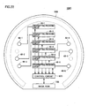
- Fig. 22 is a block diagram showing a planar structure of semiconductor storage device 100C according to the fourth embodiment of the invention.
- each of semiconductor storage devices 100C includes solar cell 50B, a control circuit 60C, mask ROM 70B, six transmitting/receiving circuits 46-1 to 46-6, and antennas 48-1 to 48-6 corresponding to respective transmitting/receiving circuits 46-1 to 46-6. These portions are formed on a wafer, and the exposed surfaces thereof are entirely covered with a sealing film (typically, made of physicochemically stable insulation substance such as silicon dioxide).
- a sealing film typically, made of physicochemically stable insulation substance such as silicon dioxide.
- control circuit 60C cooperates with transmitting/receiving circuits 46-1 to 46-6 to form an ad-hoc network with respect to at least one neighboring semiconductor storage device 100C. Specifically, control circuit 60C determines whether the stored data of semiconductor storage device 100C to which control circuit 60C belongs is a target of a data request command or not, when one of transmitting/receiving circuits 46-1 to 46-6 receives this data request command from neighboring semiconductor storage device 100C. When it is the target, control circuit 60C reads the requested data from mask ROM 70B and transmits it to neighboring semiconductor storage device 100C. When it is not the target, control circuit 60C transfers the received data request command to another neighboring semiconductor storage device 100C. Specific communication processing will be described later.
- Transmitting/receiving circuits 46-1 to 46-6 receive the electric power from solar cell 50B, and excite corresponding antennas 48-1 to 48-6 according to the command provided from control circuit 60C, respectively. Thereby, transmitting/receiving circuits 46-1 to 46-6 transmit radio signal (modulation signal) to neighboring semiconductor storage devices 100C. Also, transmitting/receiving circuits 46-1 to 46-6 decode the radio signal received through corresponding antennas 48-1 to 48-6 from another semiconductor memory device 100C for outputting the obtained data to control circuit 60C.
- Solar cell 50B and mask ROM 70B are substantially the same as those in semiconductor storage device 100B according to the third embodiment, and therefore description thereof is not repeated.
- sectional structures of semiconductor storage device 100C according to the present embodiment are substantially the same as those of semiconductor storage device 100B according to the third embodiment, and therefore description thereof is not repeated.
- antennas 48-1 to 48-6 formed on the wafer surface are spaced from each other by a predetermined distance for preventing the interference between the radio signals. More specifically, antennas 48-1 to 48-6 are arranged on the same circle spaced by a predetermined distance from the center of the wafer, and are spaced from each other by a predetermined circumferential angle.
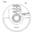
- Fig. 23 schematically shows an antenna arrangement in semiconductor storage device 100C according to the third embodiment of the invention.
- antennas 48-1 to 48-3 are arranged on a left part of the circle, i.e., a part on the left side of the sheet of the figure, and antennas 48-4 to 48-6 are arranged on a right part of the circle.
- Antennas 48-1 to 48-3 are symmetrical with respect to antennas 48-4 to 48-6 about the center of the wafer.
- the circumferential angle between antennas 48-1 and 48-2 is about twice as large as that between antennas 48-2 and 48-3.
- the circumferential angle between antennas 48-6 and 48-5 is about twice as large as that between antennas 48-5 and 48-4. This arrangement of antennas 48-1 to 48-6 can avoid crosstalk between neighboring semiconductor storage devices 100C arranged in a three-dimensional fashion as described below.
- Fig. 23(A) shows an "HM-ML arrangement" in which antennas 48-2 and 48-3 of semiconductor device 100C arranged on the left side of the sheet of the figure intersect lines H and M, respectively, and antennas 48-4 and 48-5 of semiconductor device 100C arranged on the right side of the sheet intersect lines M and L, respectively.
- Fig. 23(B) shows an "ML-HM arrangement" in which antennas 48-2 and 48-3 of semiconductor device 100C arranged on the left side of the sheet of the figure intersect lines M and L, respectively, and antennas 48-4 and 48-5 of semiconductor device 100C arranged on the right side of the sheet intersect lines H and M, respectively.
- Fig. 23(C) shows an "HL-HL arrangement" in which antennas 48-1 and 48-2 of semiconductor device 100C arranged on the left side of the sheet of the figure intersect lines H and L, respectively, and antennas 48-5 and 48-6 of semiconductor device 100C arranged on the right side of the sheet intersect lines H and L, respectively.
- Fig. 24 schematically shows a positional relationship in semiconductor device 100C in the case where storage system 500 shown in Fig. 21 is formed.
- characters "HL", “HM” and "HL” correspond to the respective patterns shown in Fig. 23 .
- semiconductor storage devices 100C neighboring to each other can perform the data transmission and reception through the antennas arranged on the same straight line.
- semiconductor storage device 100C indicated by characters "HL” has the antennas located to intersect lines H and L shown in Fig. 23
- semiconductor storage device 100C indicated by characters “HM” has the antennas located to intersect lines H and M shown in Fig. 23 . Therefore, the antennas of respective semiconductor devices 100C are present in the positions of "H" with respect to the vertical direction of the sheet of Fig. 24 , i.e., on the same straight line H extending in the lateral direction of the sheet. Therefore, neighboring semiconductor storage devices 100C perform the data transmission and reception through the two antennas located on straight line H.
- the positions of the antennas used for the data communications between neighboring semiconductor storage devices 100C on the front surface side of semiconductor storage device 100C, i.e., on the right side of the sheet of Fig. 24 can be different from those on the rear surface side of semiconductor storage device 100C, i.e., on the left side of the sheet of Fig. 24 .
- the positions of the antennas used for the data transmission and reception between semiconductor storage devices 100C arranged on the uppermost side of the sheet of Fig. 24 and semiconductor memory devices 100C neighboring to them change cyclically in the order of "H", "M", "L”, "H", ⁇ .
- a network topology of storage system 500 shown in Fig. 21 is two-dimensional. In storage system 500 according to the present embodiment, therefore, each semiconductor storage device 100C performs the control according to a path setting protocol to form dynamically a logical communication path.
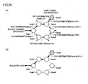
- the path setting protocol relating to the data transmission will now be described with reference to Figs. 25 and 26 .
- Fig. 25 illustrates the path setting protocol in storage system 500 according to the fourth embodiment of the invention.
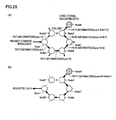
- Fig. 26 illustrates processing in the case where a network shown in Fig. 25 has a failure.
- semiconductor storage devices 100C may also be referred to as "Node 1 to Node 7" for the sake of convenience, and it is assumed that reading unit 30C neighbors to semiconductor storage device 100C corresponding to Node 1.
- the topology shown in Figs. 25 and 26 is an example of the logical connection relationship between the Nodes, and may be different from the actual positional relationship of semiconductor storage devices 100C.
- a request command is transmitted to Node 1.
- this request command includes a message requesting the reading of the data stored in Node 4. This request command is handled as a broadcast message.
- Each Node determines based on the details of the request command whether the data stored in itself includes the requested data or not. When the Node determines that the data stored in itself does not include the requested data, the Node transfers the request command of interest to the another neighboring Node different from the sender of the request command. When there are several neighboring Nodes, the request command may be transferred to one or mode Nodes.
- Fig. 25(A) shows the case where Node 1 transfers the received request command to Node 2 and Node 5.
- each Node adds, as path information, its own information (i.e., information about the Node of interest) to the request command to be transferred to the neighboring Node.
- its own information i.e., information about the Node of interest
- each of Node 2 and Node 5 receiving the request command from Node 1 determines whether the data stored in itself includes the requested data or not. Each Node determines that the data stored in itself does not include the requested data. Therefore, each of Node 2 and Node 5 adds, as the path information, the information about itself to the received request command, and transfers the request command to the neighboring Node. Thus, as shown in Fig. 25(A) , "Node 1+2" is added as the path information to the request command transferred from Node 2 to Node 3, and "Node 1+2" is added as the path information to the request command transferred from Node 5 to Node 6.
- processing is performed subsequently, and the transmission request is finally transferred through the two paths to Node 3.
- Node 3 receiving the same transmission requests refers to the path information added thereto, and transfers the transmission request relayed via a smaller number of Nodes to neighboring Node 4.
- processing may be configured to transfer only the transmission request that reached the Node earlier than the other.
- Node 4 determines that the data stored in itself includes the requested data.
- Node 4 reads out the requested data stored in its own mask ROM 70B, and returns the read data to the Node of the sender of the request command.
- the data transmitted from Node 4 bears the path information added thereto.
- This path information is produced based on the path information added to the received transmission request and, in the example shown in Fig. 25(B) , "Node 4+3+2+1" is added as the path information.
- the requested data is transferred through the Nodes, and is finally output or transmitted from Node 1 to reading unit 30C ( Fig. 21 ).
- the data can be read out in parallel through the two paths between Node 1 and Node 4. This can increase the read speed.
- Node 4 When Node 4 receives the request command transferred from Node 3, Node 4 reads out the requested data stored its own mask ROM 70B, and sends the read data to the Node of the sender of the request command. In this operation, the data read out from Node 4 is transferred in the order of Node 4, Node 3, Node 7, Node 6 and Node 5 based on the path information "Node 1+5+7+3" added to the request command, and reaches Node 1.
- semiconductor storage devices 100C forming storage system 500 can be freely designed. Further, the order of arrangement of semiconductor storage devices 100C can be freely designed.
- the highly reliable storage system can be implemented by increasing redundancy.
- the fourth embodiment described above may be configured to generate the internal electric power in each semiconductor storage device by externally supplying the electromagnetic energy (alternating magnetic flux).
- a specific structure for it is substantially the same as that of the modification of the third embodiment, and therefore description thereof is not repeated.
- the structure using the light energy (solar cell) or the structure using the electromagnetic energy is used as the structure for supplying the energy to the semiconductor storage device in the non-contact fashion.
- the structure using the light energy (solar cell) or the structure using the electromagnetic energy is used as the structure for supplying the energy to the semiconductor storage device in the non-contact fashion.
- another structure may be used.
- a structure of externally supplying thermal energy may be employed.
- a thermoelectric converter element having the Seebeck effect may be formed on each semiconductor storage device.
- thermal energy is externally supplied to each semiconductor storage device.
- a thermal change is caused in each semiconductor device.
- the internal electric power can be generated.
Landscapes
- Semiconductor Memories (AREA)
- Power Sources (AREA)
- Non-Volatile Memory (AREA)
- Read Only Memory (AREA)
- Photovoltaic Devices (AREA)
Priority Applications (1)
| Application Number | Priority Date | Filing Date | Title |
|---|---|---|---|
| EP11181670.8A EP2397976B1 (de) | 2007-10-02 | 2008-09-26 | Halbleiterspeicheranordnung und Speichersystem |
Applications Claiming Priority (3)
| Application Number | Priority Date | Filing Date | Title |
|---|---|---|---|
| JP2007258836A JP5005486B2 (ja) | 2007-10-02 | 2007-10-02 | 記憶システム |
| JP2008182931A JP5062758B2 (ja) | 2008-07-14 | 2008-07-14 | 記憶システムおよびそれに用いられる半導体記憶装置 |
| PCT/JP2008/067490 WO2009044677A1 (ja) | 2007-10-02 | 2008-09-26 | 半導体記憶装置および記憶システム |
Related Child Applications (1)
| Application Number | Title | Priority Date | Filing Date |
|---|---|---|---|
| EP11181670.8A Division-Into EP2397976B1 (de) | 2007-10-02 | 2008-09-26 | Halbleiterspeicheranordnung und Speichersystem |
Publications (3)
| Publication Number | Publication Date |
|---|---|
| EP2199954A1 true EP2199954A1 (de) | 2010-06-23 |
| EP2199954A4 EP2199954A4 (de) | 2011-03-09 |
| EP2199954B1 EP2199954B1 (de) | 2012-09-12 |
Family
ID=40526106
Family Applications (2)
| Application Number | Title | Priority Date | Filing Date |
|---|---|---|---|
| EP11181670.8A Not-in-force EP2397976B1 (de) | 2007-10-02 | 2008-09-26 | Halbleiterspeicheranordnung und Speichersystem |
| EP08835488A Not-in-force EP2199954B1 (de) | 2007-10-02 | 2008-09-26 | Halbleiterspeicheranordnung und speichersystem |
Family Applications Before (1)
| Application Number | Title | Priority Date | Filing Date |
|---|---|---|---|
| EP11181670.8A Not-in-force EP2397976B1 (de) | 2007-10-02 | 2008-09-26 | Halbleiterspeicheranordnung und Speichersystem |
Country Status (4)
| Country | Link |
|---|---|
| US (1) | US8655350B2 (de) |
| EP (2) | EP2397976B1 (de) |
| CN (1) | CN101816011B (de) |
| WO (1) | WO2009044677A1 (de) |
Families Citing this family (1)
| Publication number | Priority date | Publication date | Assignee | Title |
|---|---|---|---|---|
| JP5374246B2 (ja) * | 2009-06-12 | 2013-12-25 | 学校法人慶應義塾 | 密封型半導体記録媒体及び密封型半導体記録装置 |
Family Cites Families (27)
| Publication number | Priority date | Publication date | Assignee | Title |
|---|---|---|---|---|
| US5253184A (en) * | 1991-06-19 | 1993-10-12 | Storage Technology Corporation | Failure and performance tracking system |
| JPH0843527A (ja) | 1994-07-29 | 1996-02-16 | Nippon Avionics Co Ltd | 非接触式個体識別システム |
| US6097292A (en) * | 1997-04-01 | 2000-08-01 | Cubic Corporation | Contactless proximity automated data collection system and method |
| JPH1063807A (ja) * | 1996-08-23 | 1998-03-06 | Hitachi Ltd | カード型情報制御装置 |
| US6104291A (en) * | 1998-01-09 | 2000-08-15 | Intermec Ip Corp. | Method and apparatus for testing RFID tags |
| JP2000251038A (ja) | 1999-03-03 | 2000-09-14 | Toshiba Corp | 無線情報記憶媒体及び無線情報記憶媒体の配置方法 |
| JP3584391B2 (ja) | 1999-07-01 | 2004-11-04 | 株式会社ケンウッド | 非接触カード読書システム、非接触カード、読書装置及び非接触カード読書方法 |
| JP2001209772A (ja) | 2000-01-25 | 2001-08-03 | Toppan Printing Co Ltd | 非接触伝達機構付icカード |
| EP1436815B1 (de) | 2001-09-18 | 2010-03-03 | Kilopass Technology, Inc. | Halbleiterspeicherzelle und speicherarray mit einem durchbruchsphänomen in einem ultradünnen dielektrikum |
| US6976197B2 (en) * | 2001-10-25 | 2005-12-13 | International Business Machines Corporation | Apparatus and method for error logging on a memory module |
| JP4289825B2 (ja) * | 2002-03-29 | 2009-07-01 | 株式会社ルネサステクノロジ | 半導体記憶装置 |
| US20030217067A1 (en) * | 2002-05-17 | 2003-11-20 | Sun Microsystems, Inc. | Method and system for conveying component data identifying a component and indicating component operating conditions |
| GB2395592B (en) | 2002-11-21 | 2006-05-17 | Hewlett Packard Co | Method of annotating an item with electronic data and apparatus therefor |
| EP1437683B1 (de) * | 2002-12-27 | 2017-03-08 | Semiconductor Energy Laboratory Co., Ltd. | Chipkarte und Buchhaltungssystem unter Verwendung der Chipkarte |
| JP4646925B2 (ja) | 2002-12-27 | 2011-03-09 | 株式会社半導体エネルギー研究所 | Icカードの作製方法 |
| US7260358B2 (en) * | 2003-06-11 | 2007-08-21 | Hewlett-Packard Development Company, L.P. | Data-storage system having a wireless connection architecture for wireless data exchange between modules |
| US7561875B1 (en) * | 2003-10-16 | 2009-07-14 | Sun Microsystems, Inc. | Method and apparatus for wirelessly testing field-replaceable units (FRUs) |
| JP4238265B2 (ja) * | 2004-04-15 | 2009-03-18 | パナソニック株式会社 | 半導体集積回路、及びこれを搭載した非接触型情報システム |
| JP2006191496A (ja) | 2005-01-07 | 2006-07-20 | Nippon Telegr & Teleph Corp <Ntt> | 外部記憶装置 |
| JP2006237454A (ja) * | 2005-02-28 | 2006-09-07 | Toshiba Corp | 半導体集積回路装置 |
| DE102005020062B4 (de) | 2005-04-29 | 2011-07-21 | Globalfoundries Inc. | Mobile drahtlose Datenspeichereinrichtung und entsprechendes Verfahren zum speichern von Daten |
| GB0515796D0 (en) | 2005-07-30 | 2005-09-07 | Mccarthy Peter | A motion capture and identification device |
| US20070158804A1 (en) * | 2006-01-10 | 2007-07-12 | Semiconductor Energy Laboratory Co., Ltd. | Semiconductor device, manufacturing method of semiconductor device, and RFID tag |
| JP5057767B2 (ja) | 2006-01-10 | 2012-10-24 | 株式会社半導体エネルギー研究所 | 半導体装置の作製方法 |
| US20080100329A1 (en) * | 2006-10-31 | 2008-05-01 | Symbol Technologies, Inc. | System and method for multi-up inline testing of radio frequency identification (RFID) inlays |
| JP5325415B2 (ja) * | 2006-12-18 | 2013-10-23 | 株式会社半導体エネルギー研究所 | 半導体装置 |
| US7795895B2 (en) * | 2007-11-28 | 2010-09-14 | Mstar Semiconductor, Inc. | Loop-back testing method and apparatus for IC |
-
2008
- 2008-09-26 US US12/681,296 patent/US8655350B2/en not_active Expired - Fee Related
- 2008-09-26 CN CN2008801098974A patent/CN101816011B/zh not_active Expired - Fee Related
- 2008-09-26 EP EP11181670.8A patent/EP2397976B1/de not_active Not-in-force
- 2008-09-26 EP EP08835488A patent/EP2199954B1/de not_active Not-in-force
- 2008-09-26 WO PCT/JP2008/067490 patent/WO2009044677A1/ja not_active Ceased
Also Published As
| Publication number | Publication date |
|---|---|
| EP2397976A3 (de) | 2012-04-04 |
| EP2397976B1 (de) | 2013-05-08 |
| EP2199954A4 (de) | 2011-03-09 |
| CN101816011A (zh) | 2010-08-25 |
| EP2199954B1 (de) | 2012-09-12 |
| HK1144607A1 (en) | 2011-02-25 |
| WO2009044677A1 (ja) | 2009-04-09 |
| EP2397976A2 (de) | 2011-12-21 |
| CN101816011B (zh) | 2013-01-02 |
| US20100214817A1 (en) | 2010-08-26 |
| US8655350B2 (en) | 2014-02-18 |
Similar Documents
| Publication | Publication Date | Title |
|---|---|---|
| Fan et al. | Steady and fair rate allocation for rechargeable sensors in perpetual sensor networks | |
| Ogundile et al. | Energy‐balanced and energy‐efficient clustering routing protocol for wireless sensor networks | |
| Biagioni et al. | Wireless sensor placement for reliable and efficient data collection | |
| Rathore et al. | Green communication for next‐generation wireless systems: Optimization strategies, challenges, solutions, and future aspects | |
| BRPI0722393A2 (pt) | protocolo de lan de rf de medição e utilização e gerenciamento de célula / nó | |
| KR20090044771A (ko) | 무선 센서 네트워크에서의 다중 경로 라우팅 방법 | |
| Karthick et al. | Trust-distrust protocol for secure routing in self-organizing networks | |
| Rinne et al. | Viability bounds of M2M communication using energy-harvesting and passive wake-up radio | |
| EP2397976B1 (de) | Halbleiterspeicheranordnung und Speichersystem | |
| Morozs et al. | Data gathering in UWA sensor networks: Practical considerations and lessons from sea trials | |
| D'Elia et al. | A self-powered WSAN for energy efficient heat distribution | |
| JP5062758B2 (ja) | 記憶システムおよびそれに用いられる半導体記憶装置 | |
| Iskandarani | Effect of Transmission Range and Grid Dimensions on Route Cost in WSN Using TABU Search Algorithm | |
| Istomin et al. | Route or flood? Reliable and efficient support for downward traffic in RPL | |
| JP5005486B2 (ja) | 記憶システム | |
| Dhanapala et al. | CSR: Convex Subspace Routing protocol for wireless sensor networks | |
| HK1144607B (en) | Semiconductor storage device and storage system | |
| Sheshashayee | Wake-up radio-enabled wireless networking: Measurements and evaluation of data collection techniques in static and mobile scenarios | |
| Viana et al. | Sensing and acting with predefined trajectories | |
| Maitra et al. | XMSN: An efficient cross‐layer protocol for mixed wireless sensor networks | |
| Chen et al. | A spatial-based multi-resolution data dissemination scheme for wireless sensor networks | |
| Belkadi et al. | EE-FTR: An Energy-Efficient Fault-Tolerant Routing Protocol for Wireless Sensor Networks | |
| Bavani et al. | Proficient Performance and Data Collection Improvement in Wireless Sensors Network over MAC Protocol | |
| Lu | Gossip algorithm in wireless sensor network | |
| Buratti et al. | Wireless sensor networks |
Legal Events
| Date | Code | Title | Description |
|---|---|---|---|
| PUAI | Public reference made under article 153(3) epc to a published international application that has entered the european phase |
Free format text: ORIGINAL CODE: 0009012 |
|
| 17P | Request for examination filed |
Effective date: 20100326 |
|
| AK | Designated contracting states |
Kind code of ref document: A1 Designated state(s): AT BE BG CH CY CZ DE DK EE ES FI FR GB GR HR HU IE IS IT LI LT LU LV MC MT NL NO PL PT RO SE SI SK TR |
|
| AX | Request for extension of the european patent |
Extension state: AL BA MK RS |
|
| DAX | Request for extension of the european patent (deleted) | ||
| A4 | Supplementary search report drawn up and despatched |
Effective date: 20110207 |
|
| RIC1 | Information provided on ipc code assigned before grant |
Ipc: G06K 19/077 20060101AFI20090428BHEP Ipc: G06F 3/033 20060101ALI20110201BHEP Ipc: G06K 19/07 20060101ALI20110201BHEP |
|
| GRAP | Despatch of communication of intention to grant a patent |
Free format text: ORIGINAL CODE: EPIDOSNIGR1 |
|
| RIC1 | Information provided on ipc code assigned before grant |
Ipc: G06K 19/077 20060101AFI20120217BHEP Ipc: G06K 19/07 20060101ALI20120217BHEP Ipc: G06F 3/033 20060101ALI20120217BHEP |
|
| GRAS | Grant fee paid |
Free format text: ORIGINAL CODE: EPIDOSNIGR3 |
|
| GRAA | (expected) grant |
Free format text: ORIGINAL CODE: 0009210 |
|
| AK | Designated contracting states |
Kind code of ref document: B1 Designated state(s): AT BE BG CH CY CZ DE DK EE ES FI FR GB GR HR HU IE IS IT LI LT LU LV MC MT NL NO PL PT RO SE SI SK TR |
|
| REG | Reference to a national code |
Ref country code: GB Ref legal event code: FG4D |
|
| REG | Reference to a national code |
Ref country code: CH Ref legal event code: EP |
|
| REG | Reference to a national code |
Ref country code: AT Ref legal event code: REF Ref document number: 575361 Country of ref document: AT Kind code of ref document: T Effective date: 20120915 |
|
| REG | Reference to a national code |
Ref country code: IE Ref legal event code: FG4D |
|
| REG | Reference to a national code |
Ref country code: DE Ref legal event code: R096 Ref document number: 602008018779 Country of ref document: DE Effective date: 20121108 |
|
| PG25 | Lapsed in a contracting state [announced via postgrant information from national office to epo] |
Ref country code: FI Free format text: LAPSE BECAUSE OF FAILURE TO SUBMIT A TRANSLATION OF THE DESCRIPTION OR TO PAY THE FEE WITHIN THE PRESCRIBED TIME-LIMIT Effective date: 20120912 Ref country code: LT Free format text: LAPSE BECAUSE OF FAILURE TO SUBMIT A TRANSLATION OF THE DESCRIPTION OR TO PAY THE FEE WITHIN THE PRESCRIBED TIME-LIMIT Effective date: 20120912 Ref country code: CY Free format text: LAPSE BECAUSE OF FAILURE TO SUBMIT A TRANSLATION OF THE DESCRIPTION OR TO PAY THE FEE WITHIN THE PRESCRIBED TIME-LIMIT Effective date: 20120912 Ref country code: NO Free format text: LAPSE BECAUSE OF FAILURE TO SUBMIT A TRANSLATION OF THE DESCRIPTION OR TO PAY THE FEE WITHIN THE PRESCRIBED TIME-LIMIT Effective date: 20121212 Ref country code: HR Free format text: LAPSE BECAUSE OF FAILURE TO SUBMIT A TRANSLATION OF THE DESCRIPTION OR TO PAY THE FEE WITHIN THE PRESCRIBED TIME-LIMIT Effective date: 20120912 |
|
| REG | Reference to a national code |
Ref country code: NL Ref legal event code: VDEP Effective date: 20120912 |
|
| REG | Reference to a national code |
Ref country code: AT Ref legal event code: MK05 Ref document number: 575361 Country of ref document: AT Kind code of ref document: T Effective date: 20120912 |
|
| REG | Reference to a national code |
Ref country code: LT Ref legal event code: MG4D Effective date: 20120912 |
|
| PG25 | Lapsed in a contracting state [announced via postgrant information from national office to epo] |
Ref country code: GR Free format text: LAPSE BECAUSE OF FAILURE TO SUBMIT A TRANSLATION OF THE DESCRIPTION OR TO PAY THE FEE WITHIN THE PRESCRIBED TIME-LIMIT Effective date: 20121213 Ref country code: LV Free format text: LAPSE BECAUSE OF FAILURE TO SUBMIT A TRANSLATION OF THE DESCRIPTION OR TO PAY THE FEE WITHIN THE PRESCRIBED TIME-LIMIT Effective date: 20120912 Ref country code: SI Free format text: LAPSE BECAUSE OF FAILURE TO SUBMIT A TRANSLATION OF THE DESCRIPTION OR TO PAY THE FEE WITHIN THE PRESCRIBED TIME-LIMIT Effective date: 20120912 Ref country code: SE Free format text: LAPSE BECAUSE OF FAILURE TO SUBMIT A TRANSLATION OF THE DESCRIPTION OR TO PAY THE FEE WITHIN THE PRESCRIBED TIME-LIMIT Effective date: 20120912 |
|
| PG25 | Lapsed in a contracting state [announced via postgrant information from national office to epo] |
Ref country code: NL Free format text: LAPSE BECAUSE OF FAILURE TO SUBMIT A TRANSLATION OF THE DESCRIPTION OR TO PAY THE FEE WITHIN THE PRESCRIBED TIME-LIMIT Effective date: 20120912 Ref country code: BE Free format text: LAPSE BECAUSE OF FAILURE TO SUBMIT A TRANSLATION OF THE DESCRIPTION OR TO PAY THE FEE WITHIN THE PRESCRIBED TIME-LIMIT Effective date: 20120912 Ref country code: EE Free format text: LAPSE BECAUSE OF FAILURE TO SUBMIT A TRANSLATION OF THE DESCRIPTION OR TO PAY THE FEE WITHIN THE PRESCRIBED TIME-LIMIT Effective date: 20120912 Ref country code: MC Free format text: LAPSE BECAUSE OF NON-PAYMENT OF DUE FEES Effective date: 20120930 Ref country code: CZ Free format text: LAPSE BECAUSE OF FAILURE TO SUBMIT A TRANSLATION OF THE DESCRIPTION OR TO PAY THE FEE WITHIN THE PRESCRIBED TIME-LIMIT Effective date: 20120912 Ref country code: IS Free format text: LAPSE BECAUSE OF FAILURE TO SUBMIT A TRANSLATION OF THE DESCRIPTION OR TO PAY THE FEE WITHIN THE PRESCRIBED TIME-LIMIT Effective date: 20130112 Ref country code: RO Free format text: LAPSE BECAUSE OF FAILURE TO SUBMIT A TRANSLATION OF THE DESCRIPTION OR TO PAY THE FEE WITHIN THE PRESCRIBED TIME-LIMIT Effective date: 20120912 Ref country code: ES Free format text: LAPSE BECAUSE OF FAILURE TO SUBMIT A TRANSLATION OF THE DESCRIPTION OR TO PAY THE FEE WITHIN THE PRESCRIBED TIME-LIMIT Effective date: 20121223 |
|
| REG | Reference to a national code |
Ref country code: CH Ref legal event code: PL |
|
| PG25 | Lapsed in a contracting state [announced via postgrant information from national office to epo] |
Ref country code: PT Free format text: LAPSE BECAUSE OF FAILURE TO SUBMIT A TRANSLATION OF THE DESCRIPTION OR TO PAY THE FEE WITHIN THE PRESCRIBED TIME-LIMIT Effective date: 20130114 Ref country code: SK Free format text: LAPSE BECAUSE OF FAILURE TO SUBMIT A TRANSLATION OF THE DESCRIPTION OR TO PAY THE FEE WITHIN THE PRESCRIBED TIME-LIMIT Effective date: 20120912 Ref country code: PL Free format text: LAPSE BECAUSE OF FAILURE TO SUBMIT A TRANSLATION OF THE DESCRIPTION OR TO PAY THE FEE WITHIN THE PRESCRIBED TIME-LIMIT Effective date: 20120912 |
|
| REG | Reference to a national code |
Ref country code: IE Ref legal event code: MM4A |
|
| PG25 | Lapsed in a contracting state [announced via postgrant information from national office to epo] |
Ref country code: AT Free format text: LAPSE BECAUSE OF FAILURE TO SUBMIT A TRANSLATION OF THE DESCRIPTION OR TO PAY THE FEE WITHIN THE PRESCRIBED TIME-LIMIT Effective date: 20120912 |
|
| PLBE | No opposition filed within time limit |
Free format text: ORIGINAL CODE: 0009261 |
|
| STAA | Information on the status of an ep patent application or granted ep patent |
Free format text: STATUS: NO OPPOSITION FILED WITHIN TIME LIMIT |
|
| PG25 | Lapsed in a contracting state [announced via postgrant information from national office to epo] |
Ref country code: BG Free format text: LAPSE BECAUSE OF FAILURE TO SUBMIT A TRANSLATION OF THE DESCRIPTION OR TO PAY THE FEE WITHIN THE PRESCRIBED TIME-LIMIT Effective date: 20121212 Ref country code: IE Free format text: LAPSE BECAUSE OF NON-PAYMENT OF DUE FEES Effective date: 20120926 Ref country code: DK Free format text: LAPSE BECAUSE OF FAILURE TO SUBMIT A TRANSLATION OF THE DESCRIPTION OR TO PAY THE FEE WITHIN THE PRESCRIBED TIME-LIMIT Effective date: 20120912 Ref country code: LI Free format text: LAPSE BECAUSE OF NON-PAYMENT OF DUE FEES Effective date: 20120930 Ref country code: CH Free format text: LAPSE BECAUSE OF NON-PAYMENT OF DUE FEES Effective date: 20120930 |
|
| 26N | No opposition filed |
Effective date: 20130613 |
|
| PG25 | Lapsed in a contracting state [announced via postgrant information from national office to epo] |
Ref country code: IT Free format text: LAPSE BECAUSE OF FAILURE TO SUBMIT A TRANSLATION OF THE DESCRIPTION OR TO PAY THE FEE WITHIN THE PRESCRIBED TIME-LIMIT Effective date: 20120912 |
|
| REG | Reference to a national code |
Ref country code: DE Ref legal event code: R097 Ref document number: 602008018779 Country of ref document: DE Effective date: 20130613 |
|
| PG25 | Lapsed in a contracting state [announced via postgrant information from national office to epo] |
Ref country code: MT Free format text: LAPSE BECAUSE OF FAILURE TO SUBMIT A TRANSLATION OF THE DESCRIPTION OR TO PAY THE FEE WITHIN THE PRESCRIBED TIME-LIMIT Effective date: 20120912 |
|
| PG25 | Lapsed in a contracting state [announced via postgrant information from national office to epo] |
Ref country code: TR Free format text: LAPSE BECAUSE OF FAILURE TO SUBMIT A TRANSLATION OF THE DESCRIPTION OR TO PAY THE FEE WITHIN THE PRESCRIBED TIME-LIMIT Effective date: 20120912 |
|
| PG25 | Lapsed in a contracting state [announced via postgrant information from national office to epo] |
Ref country code: LU Free format text: LAPSE BECAUSE OF NON-PAYMENT OF DUE FEES Effective date: 20120926 |
|
| PG25 | Lapsed in a contracting state [announced via postgrant information from national office to epo] |
Ref country code: HU Free format text: LAPSE BECAUSE OF FAILURE TO SUBMIT A TRANSLATION OF THE DESCRIPTION OR TO PAY THE FEE WITHIN THE PRESCRIBED TIME-LIMIT Effective date: 20080926 |
|
| REG | Reference to a national code |
Ref country code: FR Ref legal event code: PLFP Year of fee payment: 9 |
|
| REG | Reference to a national code |
Ref country code: FR Ref legal event code: PLFP Year of fee payment: 10 |
|
| REG | Reference to a national code |
Ref country code: FR Ref legal event code: PLFP Year of fee payment: 11 |
|
| PGFP | Annual fee paid to national office [announced via postgrant information from national office to epo] |
Ref country code: DE Payment date: 20180920 Year of fee payment: 11 Ref country code: FR Payment date: 20180925 Year of fee payment: 11 |
|
| PGFP | Annual fee paid to national office [announced via postgrant information from national office to epo] |
Ref country code: GB Payment date: 20180919 Year of fee payment: 11 |
|
| REG | Reference to a national code |
Ref country code: DE Ref legal event code: R119 Ref document number: 602008018779 Country of ref document: DE |
|
| PG25 | Lapsed in a contracting state [announced via postgrant information from national office to epo] |
Ref country code: DE Free format text: LAPSE BECAUSE OF NON-PAYMENT OF DUE FEES Effective date: 20200401 |
|
| GBPC | Gb: european patent ceased through non-payment of renewal fee |
Effective date: 20190926 |
|
| PG25 | Lapsed in a contracting state [announced via postgrant information from national office to epo] |
Ref country code: GB Free format text: LAPSE BECAUSE OF NON-PAYMENT OF DUE FEES Effective date: 20190926 Ref country code: FR Free format text: LAPSE BECAUSE OF NON-PAYMENT OF DUE FEES Effective date: 20190930 |