EP2199841A1 - Lichtwellenlängenselektives Bauteil - Google Patents
Lichtwellenlängenselektives Bauteil Download PDFInfo
- Publication number
- EP2199841A1 EP2199841A1 EP08305953A EP08305953A EP2199841A1 EP 2199841 A1 EP2199841 A1 EP 2199841A1 EP 08305953 A EP08305953 A EP 08305953A EP 08305953 A EP08305953 A EP 08305953A EP 2199841 A1 EP2199841 A1 EP 2199841A1
- Authority
- EP
- European Patent Office
- Prior art keywords
- folding mirror
- light
- component
- wavelength selective
- spectral
- Prior art date
- Legal status (The legal status is an assumption and is not a legal conclusion. Google has not performed a legal analysis and makes no representation as to the accuracy of the status listed.)
- Withdrawn
Links
- 230000003287 optical effect Effects 0.000 title claims description 17
- 239000006185 dispersion Substances 0.000 claims abstract description 40
- 230000003595 spectral effect Effects 0.000 claims abstract description 37
- 239000000835 fiber Substances 0.000 claims description 23
- 238000000034 method Methods 0.000 claims description 5
- XUIMIQQOPSSXEZ-UHFFFAOYSA-N Silicon Chemical compound [Si] XUIMIQQOPSSXEZ-UHFFFAOYSA-N 0.000 claims description 4
- 239000004973 liquid crystal related substance Substances 0.000 claims description 4
- 229910052710 silicon Inorganic materials 0.000 claims description 4
- 239000010703 silicon Substances 0.000 claims description 4
- 239000013307 optical fiber Substances 0.000 claims description 2
- FGUUSXIOTUKUDN-IBGZPJMESA-N C1(=CC=CC=C1)N1C2=C(NC([C@H](C1)NC=1OC(=NN=1)C1=CC=CC=C1)=O)C=CC=C2 Chemical compound C1(=CC=CC=C1)N1C2=C(NC([C@H](C1)NC=1OC(=NN=1)C1=CC=CC=C1)=O)C=CC=C2 FGUUSXIOTUKUDN-IBGZPJMESA-N 0.000 claims 1
- 238000009434 installation Methods 0.000 description 4
- 239000000463 material Substances 0.000 description 3
- 238000001228 spectrum Methods 0.000 description 2
- 230000000295 complement effect Effects 0.000 description 1
- 230000000694 effects Effects 0.000 description 1
- 239000004744 fabric Substances 0.000 description 1
- 238000007654 immersion Methods 0.000 description 1
- 238000004519 manufacturing process Methods 0.000 description 1
- 239000011159 matrix material Substances 0.000 description 1
- -1 multiplexers Substances 0.000 description 1
- 238000000926 separation method Methods 0.000 description 1
Images

Classifications
-
- G—PHYSICS
- G02—OPTICS
- G02B—OPTICAL ELEMENTS, SYSTEMS OR APPARATUS
- G02B6/00—Light guides; Structural details of arrangements comprising light guides and other optical elements, e.g. couplings
- G02B6/24—Coupling light guides
- G02B6/26—Optical coupling means
- G02B6/28—Optical coupling means having data bus means, i.e. plural waveguides interconnected and providing an inherently bidirectional system by mixing and splitting signals
- G02B6/293—Optical coupling means having data bus means, i.e. plural waveguides interconnected and providing an inherently bidirectional system by mixing and splitting signals with wavelength selective means
- G02B6/29304—Optical coupling means having data bus means, i.e. plural waveguides interconnected and providing an inherently bidirectional system by mixing and splitting signals with wavelength selective means operating by diffraction, e.g. grating
- G02B6/29305—Optical coupling means having data bus means, i.e. plural waveguides interconnected and providing an inherently bidirectional system by mixing and splitting signals with wavelength selective means operating by diffraction, e.g. grating as bulk element, i.e. free space arrangement external to a light guide
- G02B6/2931—Diffractive element operating in reflection
-
- G—PHYSICS
- G02—OPTICS
- G02B—OPTICAL ELEMENTS, SYSTEMS OR APPARATUS
- G02B6/00—Light guides; Structural details of arrangements comprising light guides and other optical elements, e.g. couplings
- G02B6/24—Coupling light guides
- G02B6/26—Optical coupling means
- G02B6/35—Optical coupling means having switching means
- G02B6/351—Optical coupling means having switching means involving stationary waveguides with moving interposed optical elements
- G02B6/3512—Optical coupling means having switching means involving stationary waveguides with moving interposed optical elements the optical element being reflective, e.g. mirror
- G02B6/3518—Optical coupling means having switching means involving stationary waveguides with moving interposed optical elements the optical element being reflective, e.g. mirror the reflective optical element being an intrinsic part of a MEMS device, i.e. fabricated together with the MEMS device
-
- G—PHYSICS
- G02—OPTICS
- G02B—OPTICAL ELEMENTS, SYSTEMS OR APPARATUS
- G02B6/00—Light guides; Structural details of arrangements comprising light guides and other optical elements, e.g. couplings
- G02B6/24—Coupling light guides
- G02B6/26—Optical coupling means
- G02B6/35—Optical coupling means having switching means
- G02B6/354—Switching arrangements, i.e. number of input/output ports and interconnection types
- G02B6/356—Switching arrangements, i.e. number of input/output ports and interconnection types in an optical cross-connect device, e.g. routing and switching aspects of interconnecting different paths propagating different wavelengths to (re)configure the various input and output links
-
- G—PHYSICS
- G02—OPTICS
- G02B—OPTICAL ELEMENTS, SYSTEMS OR APPARATUS
- G02B6/00—Light guides; Structural details of arrangements comprising light guides and other optical elements, e.g. couplings
- G02B6/24—Coupling light guides
- G02B6/26—Optical coupling means
- G02B6/28—Optical coupling means having data bus means, i.e. plural waveguides interconnected and providing an inherently bidirectional system by mixing and splitting signals
- G02B6/293—Optical coupling means having data bus means, i.e. plural waveguides interconnected and providing an inherently bidirectional system by mixing and splitting signals with wavelength selective means
- G02B6/29304—Optical coupling means having data bus means, i.e. plural waveguides interconnected and providing an inherently bidirectional system by mixing and splitting signals with wavelength selective means operating by diffraction, e.g. grating
- G02B6/29305—Optical coupling means having data bus means, i.e. plural waveguides interconnected and providing an inherently bidirectional system by mixing and splitting signals with wavelength selective means operating by diffraction, e.g. grating as bulk element, i.e. free space arrangement external to a light guide
- G02B6/29307—Optical coupling means having data bus means, i.e. plural waveguides interconnected and providing an inherently bidirectional system by mixing and splitting signals with wavelength selective means operating by diffraction, e.g. grating as bulk element, i.e. free space arrangement external to a light guide components assembled in or forming a solid transparent unitary block, e.g. for facilitating component alignment
Definitions
- the present invention relates to optical wavelength selective components such as but not limited to an optical switch typically used in fiber network nodes.
- Wavelength selective operations such as for example wavelength selective switchings are used frequently in optical communications for example in Wavelength Division Multiplexing (WDM), or for example in channel equalization, wavelength blockers, optical programmable filters, dispersion compensators and the like.
- WDM Wavelength Division Multiplexing
- the existing methods are typically based on separating all the wavelength channels incident into a fiber node by using a discrete multiplexer or the like.
- the individual wavelength channels are then switched by optical or electronic switches and further recombined and routed to the egress fibers also using discrete multiplexers.
- Cost is incurred not only due to the cost of the switching fabric, but also due to the cost of the discrete multiplexers needed (one for each connected fiber) as well as by the interconnection fibers (for example for a 40 channel system, forty fiber jumpers are required for each connected fiber).
- the large size of the device is in a significant part due to the use of a switching matrix, multiplexers, and fiber panels to connect the switches and the multiplexers together. Power consumption is mainly significant with respect to the switches, in particular if electronic switches are used, nevertheless the multiplexers which require active temperature control also consume a significant level of power. Further the installation of the switching node will require many, typically in the order of hundreds, fibers to be connected thereby requiring significant installation time and in addition such installation may be susceptible to connection errors and to impacts of faulty fiber jumpers.
- Some embodiments of the invention feature a new structure which allows for building a compact wavelength selective component.
- the wavelength selective component comprises a dispersion grating configured to receive and disperse an input light beam into a plurality of spectral components of light beams; a plurality of optically reflective elements comprising at least one first optically reflective element configured to receive a spectral component of light beam from said plurality of spectral components of light beams and reflect the spectral component of light beam to a second optically reflective element configured to receive said spectral component of light beam and reflect the same toward an output optical fiber; and a folding mirror, configured to cooperate with said dispersion grating, said first reflective element and said second reflective element in reflecting said spectral component of light beam.
- the folding mirror may be adapted for reflecting an input light beam toward the dispersion grating.
- the dispersion grating may be configured to reflect spectral components of an incident light in angularly separated beams.
- the optically reflective elements may be microelectromechanical elements or a plurality of pixels of a liquid crystal on silicon device in phase amplitude modulation mode.
- the folding mirror may be a fixed curved folding mirror or a partially flat folding mirror.
- the wavelength selective components may be an optical switch.
- Figure 1 schematically represents a structure of a dispersion grating 1 suitable for use in the wavelength selective component according to embodiments of the invention.
- the grating 1 is preferably capable of providing a high level of dispersion in relatively small volume.
- the grating 1 comprises a pattern of dispersive lines 11 (hereinafter, dispersive pattern) with a grating period of about 4250 lines per millimeter and is made of a high refractive index optical material, the index being about or more than 3, such as for example Silicon.
- the grating is a so called immersion grating, were a light beam 12 first enters the high refractive index material 13 and is deflected according to Snell's law.
- This type of grating provides a dispersion level that is considerably (for example 8 times) higher than a conventional dispersion grating, allows to substantially reduce the size of grating-based devices such as switches or demultiplexers, but more importantly the grating makes it more practical to design new optical arrangements for more complex devices.
- a free space demultiplexer which has a typical size of 30mmx20mmx60mm, can be designed in a more reduced size, for example about 15mmx5mmx2mm.
- FIG. 2 is a schematic representation of an assembly 2 of reflective elements with the dispersion grating 1 of figure 1 included in the assembly 2.
- the assembly 2 comprises a plurality of reflective elements 21.
- the reflective elements are arranged in the form of an array of rows.
- the arrangement of the reflective elements may be comprised of a number K of rows of first reflective elements 21 i (hereinafter referred to as input reflective elements) which are adapted to receive incoming light from K corresponding input fibers (connected to the assembly) and preferably the same number K of second reflective elements 21o (hereinafter referred to as output reflective elements) adapted to redirect the light (after reflections) to output fibers (connected to the assembly).
- the assembly 2 comprises 2K rows of reflective elements.
- K is assumed to be four, thus eight rows of reflective elements 21 are provide in the array.
- K may change between 3 and 10 for typical network architecture. Every fiber connected can carry N wavelength where N is typically from 32 to 40 for metro regional networks and larger than 40 for long haul networks.
- the array of reflective elements 21 may be arranged for example in high fill factor rows, and low fill factor columns (however it is to be noted that figure 2 is not made in scale).
- the reflective elements may have a separation of about 0.1 mm from each other in a row, for a typical width of 0.9mm per reflective element and the rows may be at distance of about 2mm or more from each other.
- the array of the input reflective elements 21i may be located as consecutive rows located next to each other, as shown for example at the upper part of the assembly 2 and the array of the output reflective elements 21o may be located as consecutive rows located next to each other, as shown for example an at the lower part of the assembly 2 in figure 2 .
- the reflective elements are made of MEMS micromirrors, they may be arranged to tilt in two directions at an angle of about ⁇ 7° tilt in each direction horizontally and about ⁇ 4° in each direction vertically.
- the wavelength selective component constructed based on the structure of such assembly, allows to connect any wavelength channel of any input fiber to the same wavelength channel of any output fiber, without major restrictions with the exception that each output fiber can only receive a particular wavelength channel from only one input fiber at a time.
- the dispersion grating 1 is placed at a convenient position on the assembly 2 in order to be able to perform a dispersive function as is described further below.
- the reflective elements 21 may be microelectromechanical systems (MEMS) constructed in the form of micromirrors.
- MEMS microelectromechanical systems
- the reflective elements may be comprised in a liquid crystal on silicon device (LCOS) in phase amplitude modulation mode. In that case multiple pixels of the liquid crystal device would perform the functionality of a single MEMS mirror.
- LCOS liquid crystal on silicon device
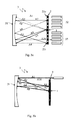
- FIG. 3a and 3b show respective schematic representations of a top view and a side view of a wavelength selective component 3 according to embodiments of the invention.
- the wavelength selective device 3 comprises an assembly of reflective elements 2 having a dispersion grating 1 located at a convenient position, for example at the center of the assembly 2, a folding mirror 31, an array of input collimators 32 and an array of output collimators 33.
- the optical wavelength selective component of figure 3 may be for example a 4x4 optical switch with 32 wavelength channels spaced at 100GHz channel width.
- figure 3a four input collimators 32 and four output collimators 33 are shown, whereas in figure 3b , only one of the eight collimators 32 and 33 is visible as this figure represents a side view of the component 3.
- any convenient number of input and output collimators may be use within the scope of the present invention.
- light incident on the folding mirror 31 is shown by means of solid-line arrows and light reflected from the folding mirror 31 is shown by means of broken-line arrows.
- the wavelength selective component 3 operates in the following manner.
- the light beam enters the component 3 in one of the fibers of the linear input collimator array 32 and is transmitted from the input collimator 32 to the folding mirror 31 as shown by arrow A1.
- the incident light is then reflected from the folding mirror 31 as shown by arrow A2 and is incident on the dispersion grating 1 where the spectral components of the incident light are angularly separated and reflected back toward the folding mirror 31 as represented in figures 3a and 3b by arrow A3.
- arrow A3 is shown in the figure.
- the dispersion grating 1 reflects a spectrum of components of the light beam comprising a plurality of components which are reflected at different angles.
- the reflected light beam, arrow A3 propagates further and impacts on the folding mirror 31 and is reflected back, arrow A4, from the folding mirror 31, whereafter it reaches an input reflective element 21i (as represented in figure 3a ) from the rows of input reflecting elements.
- each input collimator 32 there is provided a row of corresponding input reflective elements 21i such that each input reflective element 21i of the row receives a different wavelength channel corresponding to spectral components of the light input buy a corresponding input collimator 32.
- the input reflective element 21 i which receives the beam, then redirects the light, as shown by arrow A5, such that the corresponding spectral component of light is directed to the folding mirror 31 and after impact on the folding mirror 31 is reflected toward a respective output reflective element 21o (as represented in figure 3a ) as shown by arrow A6.
- the incident component of light is once again reflected back to the folding mirror 31 arrow A7, and then reflected from the folding mirror 31 toward the dispersion grating 1 as show by arrow A8.
- the dispersion grating 1 is adapted to redirect the beam (the spectral component of the light) in such a way that it will couple into a desired output fiber in the output collimator 33. This is done by a first reflection of the beam from the dispersion grating 1 to the folding mirror 31 as show by arrow A9, and a subsequent reflection of the beam from the folding mirror 31 to an output collimator 33 as shown by arrow A10.
- the position and the tilt angle of the input reflective elements 21i as well as the output reflective elements 21 o are predetermined and preferably fixed in such a way that a complete path for the light in traveling from an input collimator 32 to the output collimator 33, including the various reflections between the folding mirror and the reflective elements are well as with the dispersion grating, is ensured.
- the reflective elements always receive the same spectral complement of the dispersed light and forward the received light toward the same output fiber (adapted to receives the same wavelength in each operation).
- the grating has a high dispersion capability, thereby being capable of dispersing the received beam in a spectrum of separate wavelengths being deflected at different angels whereas the reduced size of such grating allows for constructing the overall structure of the component with a relatively low volume.
- Such an optical component may be manufactured as small as 45mmx70mmx90mm.
- the curved folding mirror may be a fixed curved folding mirror or alternatively it may be a partially flat folding mirror.
- folding in reference to the mirror is meant to refer to a capability to reuse part of the optical system multiple time, thus to "fold the optical system” such that the overall size of the system is reduced.
- the folding mirror configuration is such that the folding mirror acts mainly as an optical Fourier Transform element.
- the folding mirror can be a single reflecting curved mirror, a combination of lens and a reflective element.
- the horizontal tilt requirement of the MEMS micromirrors may be reduced from ⁇ 7° to ⁇ 1°, however this may require an increase in the size of the component in length by a factor of about 1.5.
- the input collimators 32 may be arranged to direct the incoming light directly to the dispersion grating 1 without the light being reflected from the folding mirror 31 to the grating.
- the input collimators may be located at a position which permits a direct impact of the incoming light on the dispersion grating.
- the input collimators may be placed at the top-left side of the wavelength selective component of figure 3a .
- the output collimators 33 may be arranged to receive the outgoing component of light directly from the grating without the light being reflected from the folding mirror 31 to the output collimators 33.
- the output collimators 33 may be located at a position which permits a direct impact of the outgoing light thereupon from the dispersion grating 1.
- the output collimators 33 may be placed at the top-left side of the wavelength selective component of figure 3a .
- a cylindrical lens with the cylinder axes parallel to the low fill factor direction of the reflective elements can be placed in front of the array of reflective elements 21 in order to reduce the tilt requirements of the reflective elements.
- the dispersion grating may be placed outside the assembly of the reflective elements.
Landscapes
- Physics & Mathematics (AREA)
- General Physics & Mathematics (AREA)
- Optics & Photonics (AREA)
- Engineering & Computer Science (AREA)
- Computer Networks & Wireless Communication (AREA)
- Mechanical Light Control Or Optical Switches (AREA)
Priority Applications (1)
| Application Number | Priority Date | Filing Date | Title |
|---|---|---|---|
| EP08305953A EP2199841A1 (de) | 2008-12-16 | 2008-12-16 | Lichtwellenlängenselektives Bauteil |
Applications Claiming Priority (1)
| Application Number | Priority Date | Filing Date | Title |
|---|---|---|---|
| EP08305953A EP2199841A1 (de) | 2008-12-16 | 2008-12-16 | Lichtwellenlängenselektives Bauteil |
Publications (1)
| Publication Number | Publication Date |
|---|---|
| EP2199841A1 true EP2199841A1 (de) | 2010-06-23 |
Family
ID=40565251
Family Applications (1)
| Application Number | Title | Priority Date | Filing Date |
|---|---|---|---|
| EP08305953A Withdrawn EP2199841A1 (de) | 2008-12-16 | 2008-12-16 | Lichtwellenlängenselektives Bauteil |
Country Status (1)
| Country | Link |
|---|---|
| EP (1) | EP2199841A1 (de) |
Citations (5)
| Publication number | Priority date | Publication date | Assignee | Title |
|---|---|---|---|---|
| US4475792A (en) * | 1982-07-27 | 1984-10-09 | The United States Of America As Represented By The Secretary Of The Navy | High resolution diffraction grating |
| WO2002086571A2 (en) * | 2001-04-25 | 2002-10-31 | Chromaplex, Inc. | Diffractive structure for high-dispersion wdm applications |
| US20030007721A1 (en) * | 2001-07-03 | 2003-01-09 | Network Photonics, Inc. | Free-space optical wavelength routing element based on stepwise controlled tilting mirrors |
| US20040156581A1 (en) * | 2001-04-13 | 2004-08-12 | Golub John E. | Optical cross connect utilizing free space optics and an array of micro mirrors |
| US20040258350A1 (en) * | 2002-05-28 | 2004-12-23 | Miller John Michael | Electrode configuration for piano MEMs micromirror |
-
2008
- 2008-12-16 EP EP08305953A patent/EP2199841A1/de not_active Withdrawn
Patent Citations (5)
| Publication number | Priority date | Publication date | Assignee | Title |
|---|---|---|---|---|
| US4475792A (en) * | 1982-07-27 | 1984-10-09 | The United States Of America As Represented By The Secretary Of The Navy | High resolution diffraction grating |
| US20040156581A1 (en) * | 2001-04-13 | 2004-08-12 | Golub John E. | Optical cross connect utilizing free space optics and an array of micro mirrors |
| WO2002086571A2 (en) * | 2001-04-25 | 2002-10-31 | Chromaplex, Inc. | Diffractive structure for high-dispersion wdm applications |
| US20030007721A1 (en) * | 2001-07-03 | 2003-01-09 | Network Photonics, Inc. | Free-space optical wavelength routing element based on stepwise controlled tilting mirrors |
| US20040258350A1 (en) * | 2002-05-28 | 2004-12-23 | Miller John Michael | Electrode configuration for piano MEMs micromirror |
Non-Patent Citations (1)
| Title |
|---|
| ROGERS G L: "Total internal reflection and hayghens' construction: the immersion grating", NATURE, NATURE PUBLISHING GROUP, LONDON, UK, vol. 168, 5 July 1947 (1947-07-05), pages 25 - 26, XP009115620, ISSN: 0028-0836 * |
Similar Documents
| Publication | Publication Date | Title |
|---|---|---|
| CA2392704C (en) | System and method of optical switching | |
| US6657770B2 (en) | Programmable optical multiplexer/demultiplexer | |
| JP3662754B2 (ja) | 波長選択性追加ードロップ装置 | |
| CA2318080C (en) | Wavelength-selective optical add/drop using tilting micro-mirrors | |
| US7088882B2 (en) | Wavelength cross-connect | |
| Fontaine et al. | N× M wavelength selective crossconnect with flexible passbands | |
| US8363991B2 (en) | Bidirectional wavelength cross connect architectures using wavelength routing elements | |
| CN102696194A (zh) | 可重构的光分插复用器及波长交叉连接器 | |
| EP3828607B1 (de) | Wellenlängenschaltgerät und -system | |
| US6845195B2 (en) | Configurable wavelength routing device | |
| EP3955037A1 (de) | Vorrichtung für optische kommunikation und wellenlängenauswahlverfahren | |
| US7321704B2 (en) | Wavelength cross connect with per port performance characteristics | |
| Ishii et al. | MEMS-based 1× 43 wavelength-selective switch with flat passband | |
| JP4865365B2 (ja) | 積層プレーナ導波回路を使用した波長選択スイッチおよび集積波長デマルチプレクサ | |
| CN101504474B (zh) | 一种梳形带状滤波器 | |
| US6798951B2 (en) | Wavelength router with a transmissive dispersive element | |
| EP2199841A1 (de) | Lichtwellenlängenselektives Bauteil | |
| CN112152750B (zh) | 一种波长选择开关以及相关装置 | |
| JP2016152610A (ja) | 光クロスコネクト装置 |
Legal Events
| Date | Code | Title | Description |
|---|---|---|---|
| PUAI | Public reference made under article 153(3) epc to a published international application that has entered the european phase |
Free format text: ORIGINAL CODE: 0009012 |
|
| AK | Designated contracting states |
Kind code of ref document: A1 Designated state(s): AT BE BG CH CY CZ DE DK EE ES FI FR GB GR HR HU IE IS IT LI LT LU LV MC MT NL NO PL PT RO SE SI SK TR |
|
| AX | Request for extension of the european patent |
Extension state: AL BA MK RS |
|
| 17P | Request for examination filed |
Effective date: 20101223 |
|
| 17Q | First examination report despatched |
Effective date: 20110118 |
|
| AKX | Designation fees paid |
Designated state(s): AT BE BG CH CY CZ DE DK EE ES FI FR GB GR HR HU IE IS IT LI LT LU LV MC MT NL NO PL PT RO SE SI SK TR |
|
| RAP1 | Party data changed (applicant data changed or rights of an application transferred) |
Owner name: ALCATEL LUCENT |
|
| STAA | Information on the status of an ep patent application or granted ep patent |
Free format text: STATUS: THE APPLICATION IS DEEMED TO BE WITHDRAWN |
|
| 18D | Application deemed to be withdrawn |
Effective date: 20120609 |