EP2198279B1 - Apparatus and method for detecting semiconductor substrate anomalies - Google Patents
Apparatus and method for detecting semiconductor substrate anomalies Download PDFInfo
- Publication number
- EP2198279B1 EP2198279B1 EP08787571A EP08787571A EP2198279B1 EP 2198279 B1 EP2198279 B1 EP 2198279B1 EP 08787571 A EP08787571 A EP 08787571A EP 08787571 A EP08787571 A EP 08787571A EP 2198279 B1 EP2198279 B1 EP 2198279B1
- Authority
- EP
- European Patent Office
- Prior art keywords
- image
- substrate
- penetrating
- semiconductor substrate
- backlight
- Prior art date
- Legal status (The legal status is an assumption and is not a legal conclusion. Google has not performed a legal analysis and makes no representation as to the accuracy of the status listed.)
- Not-in-force
Links
Images


Classifications
-
- G—PHYSICS
- G06—COMPUTING OR CALCULATING; COUNTING
- G06T—IMAGE DATA PROCESSING OR GENERATION, IN GENERAL
- G06T7/00—Image analysis
- G06T7/0002—Inspection of images, e.g. flaw detection
- G06T7/0004—Industrial image inspection
-
- G—PHYSICS
- G01—MEASURING; TESTING
- G01N—INVESTIGATING OR ANALYSING MATERIALS BY DETERMINING THEIR CHEMICAL OR PHYSICAL PROPERTIES
- G01N21/00—Investigating or analysing materials by the use of optical means, i.e. using sub-millimetre waves, infrared, visible or ultraviolet light
- G01N21/84—Systems specially adapted for particular applications
- G01N21/88—Investigating the presence of flaws or contamination
- G01N21/95—Investigating the presence of flaws or contamination characterised by the material or shape of the object to be examined
- G01N21/9501—Semiconductor wafers
- G01N21/9505—Wafer internal defects, e.g. microcracks
-
- H—ELECTRICITY
- H10—SEMICONDUCTOR DEVICES; ELECTRIC SOLID-STATE DEVICES NOT OTHERWISE PROVIDED FOR
- H10P—GENERIC PROCESSES OR APPARATUS FOR THE MANUFACTURE OR TREATMENT OF DEVICES COVERED BY CLASS H10
- H10P72/00—Handling or holding of wafers, substrates or devices during manufacture or treatment thereof
- H10P72/06—Apparatus for monitoring, sorting, marking, testing or measuring
- H10P72/0616—Monitoring of warpages, curvatures, damages, defects or the like
-
- G—PHYSICS
- G06—COMPUTING OR CALCULATING; COUNTING
- G06T—IMAGE DATA PROCESSING OR GENERATION, IN GENERAL
- G06T2207/00—Indexing scheme for image analysis or image enhancement
- G06T2207/10—Image acquisition modality
- G06T2207/10141—Special mode during image acquisition
- G06T2207/10152—Varying illumination
-
- G—PHYSICS
- G06—COMPUTING OR CALCULATING; COUNTING
- G06T—IMAGE DATA PROCESSING OR GENERATION, IN GENERAL
- G06T2207/00—Indexing scheme for image analysis or image enhancement
- G06T2207/30—Subject of image; Context of image processing
- G06T2207/30108—Industrial image inspection
- G06T2207/30148—Semiconductor; IC; Wafer
Definitions
- the present invention relates to an apparatus and method for detecting anomalies in semiconductor substrates.
- quality control is very important at every stage of the manufacturing process.
- This quality control is to a high extend directed to detection of defects, in particular semiconductor substrate anomalies, such as cracks and micro-cracks, scratches, dirt, voids, etc. Since even micro-cracks, penetrating or non-penetrating in the substrate, can cause breaking of the substrate during further processing, it is very important to be able to detect these cracks in an early stage of processing.
- semiconductor substrate anomalies such as cracks and micro-cracks, scratches, dirt, voids, etc. Since even micro-cracks, penetrating or non-penetrating in the substrate, can cause breaking of the substrate during further processing, it is very important to be able to detect these cracks in an early stage of processing.
- polycrystalline silicon substrates are used which are very brittle. If micro-cracks are present, likely the substrate will break during further processing.
- Quality control of a semiconductor substrate relies heavily on optical inspection, because for detecting anomalies optical inspection methods are beneficial in terms of throughput compared to other inspection methods.
- a common method to optically detect anomalies on semiconductor substrates compares an image of the substrate part to be inspected with an image of such substrate part containing substantially no anomalies of at least any anomalies of the kind to be detected.
- the first is usually called the inspection image, while the latter is usually called the reference image.
- the reference image is then subtracted from the inspection image.
- the pixel values which after subtraction are higher than a fixed threshold value are labeled as surface anomaly.
- this method can only be applied if the reference image has substantially the same gray values, i.e. the same background image, as the inspection image. Further, it can only be applied if there is no geometrical variation, e.g. scaling or distortion, between the inspection and reference image, and if both images can be well aligned in order to subtract images from exactly corresponding substrate parts from each other and in order to not cause false positives by misalignment.
- An example demonstrating the shortcomings of a referential inspection method is the inspection of polycrystalline silicon substrates used in solar cell production.
- the pattern of crystal boundaries at their surface is never identical. Consequently, a reference image having the same gray values as the inspection image can never be captured.
- EP-A1-0 985 924 A second example of a method and apparatus for detecting micro-cracks is described in EP-A1-0 985 924 , wherein front infrared illumination above 2 microns in a certain angle is applied. To that extend, an expensive low resolution camera is used.
- the present invention meets the above objectives by providing a method which comprises image processing using multlplication of a high-pass convolution filtered image and a weight image and by providing an apparatus for performing such method, preferably using a single camera.
- the present invention is directed to a method for detecting anomalies in a semiconductor substrate, such as penetrating and non-penetrating micro-cracks, in particular in a polycrystalline silicon substrate, comprising the steps of
- the invention is directed to an apparatus using such a method for detecting anomalies in a semiconductor substrate, in particular in a polycrystalline silicon substrate, which is characterized in that it comprises
- the present invention provides a method for detecting anomalies in a semiconductor substrate comprising the steps of
- convolution filtering may attenuate low-frequency image content, whilst passing or even accentuating the high frequencies.
- high-pass convolution filtering is used in order to accentuate in G(I) anomalies like micro-cracks and voids, but also crystal boundaries.
- These convolution filters are characterized by the large, weight at the centre of the pixel neighborhood, surrounded by smaller, mostly opposite signed weights. The value of the centre pixel dominates the calculation of the new pixel value, whilst the surrounding values help to reduce the effect of the large weight. This gives the effect of accentuating regions of large, rapid change in pixel value, and making areas of constant pixel value almost unaffected.
- surface anomalies and in particular micro-cracks may be distinguished from crystal boundaries, thereby enabling to detect these anomalies even in case of semiconductor substrates with non-repetitive pattern such as poly-silicon and to select defective substrates.
- Generating high-pass convolution filtered image G(I) may be realized by a Laplacian filter.
- high-pass convolution filtering also multi-directional convolution filtering such as a Gabor filter may be used.
- the first weight image W1 may be generated by fuzzy weighting of image I.
- a fuzzy weighting function gives for example pixels with a grey value within a certain range a weight value between 0 and 1. Pixels with grey values below the range may get weight value 0 and pixels with grey values above the range may get weight value 1, or any other function depending on the kind of substrate anomaly to be detected.
- the fuzzy weighting function may be implemented as a lookup table.
- the first weight image W1 may be generated by threshold filtering, meaning binarizing image 1.
- G(I) may be generated by a 3X3 Laplace convolution filter and the first weight image W1 may be generated by threshold filtering image I.
- the step of making an inspection image I may comprise illuminating the substrate with a backlight having wavelengths where the substrate is transparent or semitransparent. Anomalies should be less transparent than the substrate or not transparent within the same wavelength range. In case of silicon substrates, the wavelength range should be in the near infrared band (NIR), and preferably between about 950 nanometer and about 1 micrometer, because silicon is transparent above 1 micrometer, semitransparent about 950 nanometer and opaque for shorter wavelengths. At these wavelengths a camera with a standard silicon based sensor may be used.
- NIR near infrared band
- the method may further comprise a step b' of making an image J of the substrate, and wherein first weight image W1 is generated by fuzzy weighting or threshold filtering of a high-pass convolution filtered image G(J) from image J.
- Image J may be captured while illuminating the substrate with diffuse front light wherein the substrate is semitransparent. Anomalies should be less transparent than the substrate or not transparent within the same wavelength range. In case of silicon substrates, the wavelength range should be within the near infrared band (NIR), and preferably around about 950 nanometer. In a more preferred embodiment, the backlight for capturing image I and the diffuse front light for capturing image J may have an identical wavelength range, because then a single camera keeping the same focus can be used to capture both pictures.
- NIR near infrared band
- G(I) may be generated by a 3X3 Laplace convolution filter and the first weight image W1 may be generated by threshold filtering of G(J) which may be generated by a 3X3 Laplace convolution filter.
- the method may further comprise the step multiplying convolution filtered image G(I) with a second weight image W2 from image I.
- Second weight image W2 may be generated by fuzzy weighting or threshold filtering of image I.
- the method is used for detecting penetrating and/or non-penetrating micro-cracks in semiconductor substrates.
- penetrating and/or non-penetrating micro-cracks may be detected in non-repetitive patterned substrates such as polycrystalline silicon.
- All methods in accordance with the present invention may be extended by a step of region growing, wherein, after the easiest detectable cracks are found, a starting pixel in these cracks (i.e. a seed point) is chosen to start the region growing (i.e. clustering).
- the methods in accordance with the present invention only using backlight may be extended with repeating the method by searching the area around found cracks, therefore generating an additional weight image with a broader threshold range.
- this extension also the ends of a crack, which are usually thinner and less penetrating than the center of the crack, may be detected.
- the present invention provides an apparatus according to claim 7.
- a single camera keeping the same focus can be used to capture images when illuminating them with backlight or illuminating them with diffuse front light. Both images may be image processed by the image processing unit to detect substrate anomalies, in particular both penetrating and non-penetrating micro-cracks.
- the apparatus may also further comprise an optical filter (f) blocking visible light.
- the apparatus may use wavelengths where the substrate is semitransparent. Anomalies should be less transparent than the substrate or not transparent within the same wavelength range. In case of silicon substrates, the wavelength range should be within the NIR range, preferably between about 935 nanometer and about 965 nanometer, and more preferably around about 950 nanometer, because silicon is semitransparent at about 950 nanometer and opaque for shorter wavelengths. At these wavelengths a camera with a standard silicon based sensor may be used.
- the backlight and/or the diffuse front light comprises LEDs which are mounted with a distance between two LEDs and at a distance from the semiconductor substrate such that the light of each LED overlaps light of at least on other LED.
- the light is diffused and is more robust against non-homogeneity of the LEDs without additional use of diffuser.
- a semiconductor substrate is provided on a means for holding a semiconductor substrate.
- the substrate is illuminated with a 950 nanometer backlight and an inspection image I is captured by a camera with a resolution between about 50 and about 100 micrometer/pixel.
- Inspection image I and all derived images have 8bit grey values, i.e. from 0 to 255.
- An image G(I) is generated by a 3X3 Laplace convolution filter, for example 1 1 1 1 -8 1 1 1 1 1 which accentuates anomalies, such as cracks, voids, foreign material included in the substrate, and crystal boundaries from image I.
- the image I is examined using image B. Therefore, in image B clustering is done with 4 neighborhood (taking only 2 vertical and 2 horizontal neighborhood pixels in account) or 8 neighborhood (taking also diagonal neighborhood pixels in account). Of these clusters, only clusters where Number of pixels > T3 AND length > T4 are kept, with T3 is preferably 10 and T4 is preferably 20. Then, clusters with a distance smaller than T5 pixels are grouped, where T5 is preferably 3. Based on this group of clusters in image B, the corresponding clusters of pixels in image I are sorted by their contrast and only a number of clusters C1 (preferably 100) with the highest contrast are kept. Thereof, a number C2 (preferably 10) of the largest clusters are kept.
- a semiconductor substrate is provided on a means for holding a semiconductor substrate.
- the substrate is illuminated with a 950 nanometer backlight and an inspection image I is captured by a camera with a resolution between about 50 and about 100 micrometer/pixel.
- the substrate is illuminated with a diffuse 950 nanometer front light and an image J is captured by the same camera.
- Inspection image I, image J and all derived images have 8bit grey values, i.e. from 0 to 255.
- An image G(I) is then generated by a 3X3 Laplace convolution filter, for example 1 1 1 1 -8 1 1 1 1 1 which accentuates anomalies, such as cracks, voids, foreign material included in the substrate, and crystal boundaries from image I.
- the image I is examined using image B. Therefore, in image B clustering is done with 4 neighborhood (taking only 2 vertical and 2 horizontal neighborhood pixels in account) or 8 neighborhood (taking also diagonal neighborhood pixels in account). Of these cluster, only clusters where Number of pixels > T3 AND length > T4 are kept, with T3 is preferably 10 and T4 is preferably 20. Then, clusters with a distance smaller than T5 pixels are grouped, where T5 is preferably 3. Based on this group of clusters in image B, the corresponding clusters of pixels in image I are sorted by their contrast and only a number of clusters C1 (preferably 100) with the highest contrast are kept. Thereof, a number C2 (preferably 10) of the largest clusters are kept.
Landscapes
- Engineering & Computer Science (AREA)
- General Physics & Mathematics (AREA)
- Physics & Mathematics (AREA)
- Immunology (AREA)
- Health & Medical Sciences (AREA)
- Biochemistry (AREA)
- General Health & Medical Sciences (AREA)
- Chemical & Material Sciences (AREA)
- Life Sciences & Earth Sciences (AREA)
- Pathology (AREA)
- Analytical Chemistry (AREA)
- Quality & Reliability (AREA)
- Computer Vision & Pattern Recognition (AREA)
- Theoretical Computer Science (AREA)
- Investigating Materials By The Use Of Optical Means Adapted For Particular Applications (AREA)
- Testing Or Measuring Of Semiconductors Or The Like (AREA)
- Image Processing (AREA)
Abstract
Description
- The present invention relates to an apparatus and method for detecting anomalies in semiconductor substrates.
- In semiconductor processing and manufacturing of semiconductor components and integrated circuits, quality control is very important at every stage of the manufacturing process. This quality control is to a high extend directed to detection of defects, in particular semiconductor substrate anomalies, such as cracks and micro-cracks, scratches, dirt, voids, etc. Since even micro-cracks, penetrating or non-penetrating in the substrate, can cause breaking of the substrate during further processing, it is very important to be able to detect these cracks in an early stage of processing. For example for solar cell production, polycrystalline silicon substrates are used which are very brittle. If micro-cracks are present, likely the substrate will break during further processing.
- Quality control of a semiconductor substrate relies heavily on optical inspection, because for detecting anomalies optical inspection methods are beneficial in terms of throughput compared to other inspection methods.
- A common method to optically detect anomalies on semiconductor substrates compares an image of the substrate part to be inspected with an image of such substrate part containing substantially no anomalies of at least any anomalies of the kind to be detected. The first is usually called the inspection image, while the latter is usually called the reference image. To compare both images, the reference image is then subtracted from the inspection image. The pixel values which after subtraction are higher than a fixed threshold value are labeled as surface anomaly.
- However, this method can only be applied if the reference image has substantially the same gray values, i.e. the same background image, as the inspection image. Further, it can only be applied if there is no geometrical variation, e.g. scaling or distortion, between the inspection and reference image, and if both images can be well aligned in order to subtract images from exactly corresponding substrate parts from each other and in order to not cause false positives by misalignment.
- In some cases a reference image having substantially the same gray values as the inspection image is unavailable simply because the semiconductor substrate to be inspected is never identical to a corresponding substrate which could be used as reference surface.
- An example demonstrating the shortcomings of a referential inspection method is the inspection of polycrystalline silicon substrates used in solar cell production. The pattern of crystal boundaries at their surface is never identical. Consequently, a reference image having the same gray values as the inspection image can never be captured.
- Methods and apparatuses have been proposed to potentially alleviate the above problem. For example in "Solar Cell Crack Inspection by Image Processing", Fu Zhuang, et al. propose a so-called non-referential method, i.e. an inspection method wherein no reference image is used. Gauss-Laplacian 5X5 filtering is used to sharpen the image, which is computationally quite expensive. Furthermore, only test results on solar cells with rather homogeneous pattern are presented.
- Another method and also an apparatus for detecting micro-cracks are described in
DE-A1-10 2005 061 785 , wherein the substrate is illuminated with infrared backlight and visible diffuse front light and wherein two substrate images are captured and image processed. To capture both images at different wavelengths, two cameras with different focal planes are needed, which is expensive and which requires a very accurate calibration of both cameras. - A second example of a method and apparatus for detecting micro-cracks is described in
EP-A1-0 985 924 , wherein front infrared illumination above 2 microns in a certain angle is applied. To that extend, an expensive low resolution camera is used. - Another exemplary known prior art solution is disclosed in patent application publication
WO 2005100961 describing imaging semiconductor structures using solid state illumination. The solutions according to this invention consist of a camera, light sources, lenses and software algorithms that are used to image and inspect semiconductor structures, including through infrared radiation. The use of various configurations of solid state lighting and software algorithms enhances the imaging and inspection. - Given the above drawbacks of prior art methods and apparatuses, it is an objective of the present invention to provide a method and apparatus for detecting semiconductor substrate anomalies, such as cracks, scratches, voids, pits, or foreign material included in the substrate, in a non-referential way In order to be able to select defective semiconductor substrates.
- In particular, it is an object of the present invention to provide a method and apparatus for detecting micro-cracks, penetrating and non-penetrating, in poly-silicon substrates.
- It is further an objective of the present invention to provide a method and apparatus for detecting semiconductor substrate anomalies including micro-cracks in a less expensive way compared to known prior art methods and apparatuses.
- The present invention meets the above objectives by providing a method which comprises image processing using multlplication of a high-pass convolution filtered image and a weight image and by providing an apparatus for performing such method, preferably using a single camera.
- The present invention is directed to a method for detecting anomalies in a semiconductor substrate, such as penetrating and non-penetrating micro-cracks, in particular in a polycrystalline silicon substrate, comprising the steps of
- a. providing a semiconductor substrate
- b. making an inspection image I of the substrate by illuminating the substrate with a backlight having wavelengths within the range of NIR, so that said penetrating and non-penetrating micro-cracks are less transparent than the substrate or not transparent,
- c. generating an image K from image I by image processing
- d. generating image B by binarizing image K
- e. examining image I using image B to determine locations of penetrating and non-penetrating micro-cracks in semiconductor substrate,
- Further, the invention is directed to an apparatus using such a method for detecting anomalies in a semiconductor substrate, in particular in a polycrystalline silicon substrate, which is characterized in that it comprises
- a. means for holding a semiconductor substrate
- b. a backlight for illuminating the substrate's backside
- c. a diffuse front light for illuminating the substrate's front side
- d. an image processing unit
- e. a camera
-
-
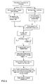
FIG 1 illustrates an embodiment of a method according to the present invention. -
FIG 2 illustrates another embodiment of a method according to the present invention. -
FIG 3 illustrates an embodiment of an apparatus according to the present invention. -
FIG 4 illustrates a first example in accordance with the present invention. -
FIG 5 illustrates a second example in accordance with the present invention. - A person skilled in the art will understand that the embodiments described below are merely illustrative in accordance with the present invention and not limiting the intended scope of the invention. Other embodiments may also be considered.
- As a first embodiment and as illustrated in
FIG 1 , the present invention provides a method for detecting anomalies in a semiconductor substrate comprising the steps of - a. providing a semiconductor substrate
- b. making an inspection image I of the substrate
- c. generating an image K from image I by image processing
- d. generating image B by binarizing image K
- e. examining image I using image B
- Depending on the filter kernel, convolution filtering may attenuate low-frequency image content, whilst passing or even accentuating the high frequencies. In the context of the present invention, high-pass convolution filtering is used in order to accentuate in G(I) anomalies like micro-cracks and voids, but also crystal boundaries. These convolution filters are characterized by the large, weight at the centre of the pixel neighborhood, surrounded by smaller, mostly opposite signed weights. The value of the centre pixel dominates the calculation of the new pixel value, whilst the surrounding values help to reduce the effect of the large weight. This gives the effect of accentuating regions of large, rapid change in pixel value, and making areas of constant pixel value almost unaffected.
- By multiplying a high-pass convolution filtered image G(I) from image I and a first weight image W1, surface anomalies and in particular micro-cracks may be distinguished from crystal boundaries, thereby enabling to detect these anomalies even in case of semiconductor substrates with non-repetitive pattern such as poly-silicon and to select defective substrates.
- Generating high-pass convolution filtered image G(I) may be realized by a Laplacian filter. As an alternative to high-pass convolution filtering, also multi-directional convolution filtering such as a Gabor filter may be used.
- The first weight image W1 may be generated by fuzzy weighting of image I. A fuzzy weighting function gives for example pixels with a grey value within a certain range a weight value between 0 and 1. Pixels with grey values below the range may get weight value 0 and pixels with grey values above the range may get
weight value 1, or any other function depending on the kind of substrate anomaly to be detected. The fuzzy weighting function may be implemented as a lookup table. - The first weight image W1 may be generated by threshold filtering, meaning
binarizing image 1. - In a preferred embodiment of the present invention, G(I) may be generated by a 3X3 Laplace convolution filter and the first weight image W1 may be generated by threshold filtering image I.
- The step of making an inspection image I may comprise illuminating the substrate with a backlight having wavelengths where the substrate is transparent or semitransparent. Anomalies should be less transparent than the substrate or not transparent within the same wavelength range. In case of silicon substrates, the wavelength range should be in the near infrared band (NIR), and preferably between about 950 nanometer and about 1 micrometer, because silicon is transparent above 1 micrometer, semitransparent about 950 nanometer and opaque for shorter wavelengths. At these wavelengths a camera with a standard silicon based sensor may be used.
- In a further embodiment in accordance with the present invention and as illustrated in
FIG 2 , the method may further comprise a step b' of making an image J of the substrate, and wherein first weight image W1 is generated by fuzzy weighting or threshold filtering of a high-pass convolution filtered image G(J) from image J. - Image J may be captured while illuminating the substrate with diffuse front light wherein the substrate is semitransparent. Anomalies should be less transparent than the substrate or not transparent within the same wavelength range. In case of silicon substrates, the wavelength range should be within the near infrared band (NIR), and preferably around about 950 nanometer. In a more preferred embodiment, the backlight for capturing image I and the diffuse front light for capturing image J may have an identical wavelength range, because then a single camera keeping the same focus can be used to capture both pictures.
- In a preferred embodiment, G(I) may be generated by a 3X3 Laplace convolution filter and the first weight image W1 may be generated by threshold filtering of G(J) which may be generated by a 3X3 Laplace convolution filter.
- In a further embodiment, the method may further comprise the step multiplying convolution filtered image G(I) with a second weight image W2 from image I. Second weight image W2 may be generated by fuzzy weighting or threshold filtering of image I.
- The method is used for detecting penetrating and/or non-penetrating micro-cracks in semiconductor substrates. In particular, penetrating and/or non-penetrating micro-cracks may be detected in non-repetitive patterned substrates such as polycrystalline silicon.
- All methods in accordance with the present invention may be extended by a step of region growing, wherein, after the easiest detectable cracks are found, a starting pixel in these cracks (i.e. a seed point) is chosen to start the region growing (i.e. clustering).
- The methods in accordance with the present invention only using backlight may be extended with repeating the method by searching the area around found cracks, therefore generating an additional weight image with a broader threshold range. By using this extension, also the ends of a crack, which are usually thinner and less penetrating than the center of the crack, may be detected.
- In another embodiment and as illustrated in
FIG 3 , the present invention provides an apparatus according to claim 7. - By using substantially the same wavelength range for backlight and diffuse front light illumination, preferably a single camera keeping the same focus can be used to capture images when illuminating them with backlight or illuminating them with diffuse front light. Both images may be image processed by the image processing unit to detect substrate anomalies, in particular both penetrating and non-penetrating micro-cracks.
- The apparatus may also further comprise an optical filter (f) blocking visible light.
- In an embodiment in accordance with the present invention, the apparatus may use wavelengths where the substrate is semitransparent. Anomalies should be less transparent than the substrate or not transparent within the same wavelength range. In case of silicon substrates, the wavelength range should be within the NIR range, preferably between about 935 nanometer and about 965 nanometer, and more preferably around about 950 nanometer, because silicon is semitransparent at about 950 nanometer and opaque for shorter wavelengths. At these wavelengths a camera with a standard silicon based sensor may be used.
- In a preferred embodiment, the backlight and/or the diffuse front light comprises LEDs which are mounted with a distance between two LEDs and at a distance from the semiconductor substrate such that the light of each LED overlaps light of at least on other LED. By overlapping the light beams, the light is diffused and is more robust against non-homogeneity of the LEDs without additional use of diffuser.
- As illustrated in
FIG 4 , a first example in accordance with the present invention is described below. - A semiconductor substrate is provided on a means for holding a semiconductor substrate. The substrate is illuminated with a 950 nanometer backlight and an inspection image I is captured by a camera with a resolution between about 50 and about 100 micrometer/pixel. Inspection image I and all derived images have 8bit grey values, i.e. from 0 to 255.
- An image G(I) is generated by a 3X3 Laplace convolution filter, for example
1 1 1 1 -8 1 1 1 1 - Further, an weight image W1 is generated by binarizing (threshold filtering) image I, wherein

where preferably
for non-penetrating cracks, voids, foreign material T0 = 0; T1 = 150
for penetrating cracks T0 = 205; T1 = 255 - Hence G(I) and W1 are pixelwise multiplied in order to distinguish between crystal boundaries and other anomalies and the resulting image K is binarized wherein

where T2 is preferably 85. - The image I is examined using image B. Therefore, in image B clustering is done with 4 neighborhood (taking only 2 vertical and 2 horizontal neighborhood pixels in account) or 8 neighborhood (taking also diagonal neighborhood pixels in account). Of these clusters, only clusters where Number of pixels > T3 AND length > T4 are kept, with T3 is preferably 10 and T4 is preferably 20. Then, clusters with a distance smaller than T5 pixels are grouped, where T5 is preferably 3. Based on this group of clusters in image B, the corresponding clusters of pixels in image I are sorted by their contrast and only a number of clusters C1 (preferably 100) with the highest contrast are kept. Thereof, a number C2 (preferably 10) of the largest clusters are kept.
- The method as illustrated in example 1 may be extended by repeating the method by searching the area around found cracks, therefore generating an image W1 wherein

where preferably T0 = 0; T1 = 230.
By using this extension also the ends of a crack, which are usually thinner and less penetrating than the center of the crack, may be detected. - As illustrated in
FIG 5 , a second example in accordance with the present invention is described below. - A semiconductor substrate is provided on a means for holding a semiconductor substrate. The substrate is illuminated with a 950 nanometer backlight and an inspection image I is captured by a camera with a resolution between about 50 and about 100 micrometer/pixel. Then the substrate is illuminated with a diffuse 950 nanometer front light and an image J is captured by the same camera. Inspection image I, image J and all derived images have 8bit grey values, i.e. from 0 to 255.
- An image G(I) is then generated by a 3X3 Laplace convolution filter, for example
1 1 1 1 -8 1 1 1 1 - Further, an weight image W1 is generated by binarizing (threshold filtering) image G(J), which is a 3X3 Laplace convolution filtering image from J, wherein
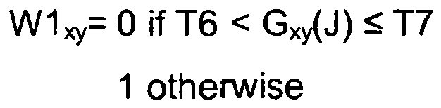
where preferably T6 = 150, T7 = 255 (both penetrating and non-penetrating cracks). - Hence G(I) and W1 are pixelwise multiplied in order to distinguish between crystal boundaries and other anomalies and the resulting image K is binarized wherein

where T2 is preferably 85. - The image I is examined using image B. Therefore, in image B clustering is done with 4 neighborhood (taking only 2 vertical and 2 horizontal neighborhood pixels in account) or 8 neighborhood (taking also diagonal neighborhood pixels in account). Of these cluster, only clusters where Number of pixels > T3 AND length > T4 are kept, with T3 is preferably 10 and T4 is preferably 20. Then, clusters with a distance smaller than T5 pixels are grouped, where T5 is preferably 3. Based on this group of clusters in image B, the corresponding clusters of pixels in image I are sorted by their contrast and only a number of clusters C1 (preferably 100) with the highest contrast are kept. Thereof, a number C2 (preferably 10) of the largest clusters are kept.
Claims (10)
- A method for detecting anomalies in a semiconductor substrate, such as penetrating and non-penetrating micro-cracks, in particular in a polycrystalline silicon substrate, comprising the steps of:a) providing a semiconductor substrate,b) making an inspection image I of the substrate by illuminating the substrate with a backlight having wavelengths within the range of NIR, so that said penetrating and non-penetrating micro-cracks are less transparent than the substrate or not transparent,c) generating an image K from image I by image processing,d) generating image B by binarizing image K,e) examining image I using image B to determine locations of said penetrating and non-penetrating micro-cracks in semiconductor substratecharacterized in that
step c) comprises multiplying a high-pass convolution filtered image G(I) from image I and a first weight image W generated by fuzzy weighting or binarizing image I, and
step e) comprises clustering image I on the basis of clustering image B by sorting clusters of image I by their contrast and selecting a predefined number of clusters of image I with the highest contrast. - A method according to claim 1, further charcterized in that it comprises step b') of making an image J of the substrate, and wherein first weight image W1 is generated by fuzzy weighting or binarizing of a high-pass convolution filtered image G(J) from image J.
- A method according to claim 1 or 2 further characterized in that it the high-pass convolution filtered image G(I) is realized by 3X3 Laplacian convolution filtering.
- A method according to any of claims 1-3, further characterized in that it comprises the step of multiplying convolution filtered image G(I) with a second weight image W2 generated by fuzzy weighting or binarizing of image I.
- A method according to claim 2, wherein step b) comprises illuminating the substrate with a backlight having wavelengths within the range of NIR and wherein step b') comprises illuminating the substrate with a diffuse front light having an identical wavelength range as the backlight.
- An apparatus using the method according to any of claims 1-5.
- An apparatus according to Claim 6, further characterized in that it comprises:a) means for holding a semiconductor substrate (a),b) a backlight for illuminating the substrate's backside (b),c) a diffuse front light for illuminating the substrate's front side (c),d) an image processing unit (d),e) a camera (e),wherein the wavelengths of the backlight and diffuse front light are within identical ranges and wherein the backlight and/or the diffuse front light comprises LEDs which are mounted with a distance between two LEDs and at a distance from the semiconductor substrate such that the light of each LED overlaps light of at least one other LED.
- An apparatus according to claim 6 or 7, further characterized in that it has a single camera (e).
- An apparatus according to any of claims 6-8, further characterized in that the wavelength is chosen from a range between 935 and 965 nanometers, and preferably amounts substantially 950 nanometers.
- An apparatus according to any of claims 6-9, further comprising an optical filter (f) blocking visible light.
Priority Applications (1)
| Application Number | Priority Date | Filing Date | Title |
|---|---|---|---|
| EP08787571A EP2198279B1 (en) | 2007-08-31 | 2008-08-29 | Apparatus and method for detecting semiconductor substrate anomalies |
Applications Claiming Priority (3)
| Application Number | Priority Date | Filing Date | Title |
|---|---|---|---|
| EP07115449 | 2007-08-31 | ||
| EP08787571A EP2198279B1 (en) | 2007-08-31 | 2008-08-29 | Apparatus and method for detecting semiconductor substrate anomalies |
| PCT/EP2008/061414 WO2009027517A1 (en) | 2007-08-31 | 2008-08-29 | Apparatus and method for detecting semiconductor substrate anomalies |
Publications (2)
| Publication Number | Publication Date |
|---|---|
| EP2198279A1 EP2198279A1 (en) | 2010-06-23 |
| EP2198279B1 true EP2198279B1 (en) | 2011-11-09 |
Family
ID=38857946
Family Applications (1)
| Application Number | Title | Priority Date | Filing Date |
|---|---|---|---|
| EP08787571A Not-in-force EP2198279B1 (en) | 2007-08-31 | 2008-08-29 | Apparatus and method for detecting semiconductor substrate anomalies |
Country Status (8)
| Country | Link |
|---|---|
| US (1) | US8379964B2 (en) |
| EP (1) | EP2198279B1 (en) |
| JP (1) | JP5192547B2 (en) |
| KR (1) | KR101192053B1 (en) |
| CN (1) | CN101796398B (en) |
| AT (1) | ATE533043T1 (en) |
| ES (1) | ES2376394T3 (en) |
| WO (1) | WO2009027517A1 (en) |
Families Citing this family (13)
| Publication number | Priority date | Publication date | Assignee | Title |
|---|---|---|---|---|
| JP2010153769A (en) * | 2008-11-19 | 2010-07-08 | Tokyo Electron Ltd | Substrate position sensing device, substrate position sensing method, film forming device, film forming method, program, and computer readable storage medium |
| DE102009017786B3 (en) * | 2009-04-20 | 2010-10-14 | Intego Gmbh | Method for detecting defects in a thin wafer wafer for a solar element and device for carrying out the method |
| US8766192B2 (en) * | 2010-11-01 | 2014-07-01 | Asm Assembly Automation Ltd | Method for inspecting a photovoltaic substrate |
| US8866899B2 (en) | 2011-06-07 | 2014-10-21 | Photon Dynamics Inc. | Systems and methods for defect detection using a whole raw image |
| JP5128699B1 (en) * | 2011-09-27 | 2013-01-23 | シャープ株式会社 | Wiring inspection method and wiring inspection apparatus |
| WO2014038012A1 (en) * | 2012-09-05 | 2014-03-13 | 株式会社島津製作所 | Solar cell inspecting apparatus |
| US10067072B2 (en) * | 2015-07-10 | 2018-09-04 | Kla-Tencor Corporation | Methods and apparatus for speckle suppression in laser dark-field systems |
| US10360477B2 (en) * | 2016-01-11 | 2019-07-23 | Kla-Tencor Corp. | Accelerating semiconductor-related computations using learning based models |
| JP6763966B2 (en) * | 2016-04-27 | 2020-09-30 | エーエスエムエル ホールディング エヌ.ブイ. | Image processing convolution algorithm for defect detection |
| KR102492053B1 (en) | 2017-08-23 | 2023-01-25 | 삼성전자주식회사 | Semiconductor manufacturing device and method of manufacturing semiconductor device using the same |
| CN107677679A (en) * | 2017-09-22 | 2018-02-09 | 武汉精测电子技术股份有限公司 | Sorting technique and device the defects of L0 pictures in a kind of AOI detection |
| CN109086827A (en) * | 2018-08-10 | 2018-12-25 | 北京百度网讯科技有限公司 | Method and apparatus for detecting monocrystaline silicon solar cell defect |
| CN110726730B (en) * | 2019-11-05 | 2022-12-06 | 黑龙江瑞兴科技股份有限公司 | Self-adaptive transmission detection device |
Citations (1)
| Publication number | Priority date | Publication date | Assignee | Title |
|---|---|---|---|---|
| US20050152146A1 (en) * | 2002-05-08 | 2005-07-14 | Owen Mark D. | High efficiency solid-state light source and methods of use and manufacture |
Family Cites Families (18)
| Publication number | Priority date | Publication date | Assignee | Title |
|---|---|---|---|---|
| JP2796316B2 (en) * | 1988-10-24 | 1998-09-10 | 株式会社日立製作所 | Defect or foreign matter inspection method and apparatus |
| JP3006090B2 (en) * | 1990-12-18 | 2000-02-07 | 株式会社日立製作所 | Green sheet manufacturing method, green sheet inspection method and apparatus therefor |
| JPH05119468A (en) * | 1991-10-29 | 1993-05-18 | Nikon Corp | Mask inspection device |
| JP3433333B2 (en) * | 1994-05-09 | 2003-08-04 | 大日本印刷株式会社 | Defect inspection method |
| US5638465A (en) * | 1994-06-14 | 1997-06-10 | Nippon Telegraph And Telephone Corporation | Image inspection/recognition method, method of generating reference data for use therein, and apparatuses therefor |
| JPH08220008A (en) * | 1995-02-15 | 1996-08-30 | Mitsubishi Electric Corp | Infrared inspection equipment |
| US6256091B1 (en) | 1997-08-25 | 2001-07-03 | Nippon Maxis Co., Ltd. | Transparent substrate mounting platform, transparent substrate scratch inspection device, transparent substrate bevelling inspection method and device, and transparent substrate inspection method |
| EP1001460B1 (en) * | 1998-10-15 | 2001-05-02 | Wacker Siltronic Gesellschaft für Halbleitermaterialien Aktiengesellschaft | Method and apparatus for detecting, monitoring and characterizing edge defects on semiconductor wafers |
| AU2002219847A1 (en) * | 2000-11-15 | 2002-05-27 | Real Time Metrology, Inc. | Optical method and apparatus for inspecting large area planar objects |
| US6809809B2 (en) * | 2000-11-15 | 2004-10-26 | Real Time Metrology, Inc. | Optical method and apparatus for inspecting large area planar objects |
| JP3784711B2 (en) * | 2000-12-20 | 2006-06-14 | 株式会社日立ハイテクノロジーズ | Defect inspection method and apparatus |
| US7142294B2 (en) | 2000-12-20 | 2006-11-28 | Hitachi, Ltd. | Method and apparatus for detecting defects |
| US7231080B2 (en) * | 2001-02-13 | 2007-06-12 | Orbotech Ltd. | Multiple optical input inspection system |
| US8077305B2 (en) * | 2004-04-19 | 2011-12-13 | Owen Mark D | Imaging semiconductor structures using solid state illumination |
| DE102004029212B4 (en) * | 2004-06-16 | 2006-07-13 | Leica Microsystems Semiconductor Gmbh | Apparatus and method for optical inspection and / or transmitted light inspection of microstructures in the IR |
| KR100598381B1 (en) | 2004-06-18 | 2006-07-07 | 삼성전자주식회사 | In-line type automatic wafer defect sorting device and control method |
| DE102005061785B4 (en) * | 2005-12-23 | 2008-04-03 | Basler Ag | Method and apparatus for detecting cracks in silicon wafers |
| JP4575886B2 (en) | 2006-02-14 | 2010-11-04 | シャープ株式会社 | Crack inspection apparatus and crack inspection method for polycrystalline semiconductor wafer |
-
2008
- 2008-08-29 AT AT08787571T patent/ATE533043T1/en active
- 2008-08-29 EP EP08787571A patent/EP2198279B1/en not_active Not-in-force
- 2008-08-29 KR KR1020107006969A patent/KR101192053B1/en not_active Expired - Fee Related
- 2008-08-29 CN CN2008801048903A patent/CN101796398B/en not_active Expired - Fee Related
- 2008-08-29 WO PCT/EP2008/061414 patent/WO2009027517A1/en not_active Ceased
- 2008-08-29 US US12/674,232 patent/US8379964B2/en active Active
- 2008-08-29 ES ES08787571T patent/ES2376394T3/en active Active
- 2008-08-29 JP JP2010522393A patent/JP5192547B2/en not_active Expired - Fee Related
Patent Citations (1)
| Publication number | Priority date | Publication date | Assignee | Title |
|---|---|---|---|---|
| US20050152146A1 (en) * | 2002-05-08 | 2005-07-14 | Owen Mark D. | High efficiency solid-state light source and methods of use and manufacture |
Also Published As
| Publication number | Publication date |
|---|---|
| US20110123091A1 (en) | 2011-05-26 |
| JP5192547B2 (en) | 2013-05-08 |
| ATE533043T1 (en) | 2011-11-15 |
| WO2009027517A1 (en) | 2009-03-05 |
| CN101796398A (en) | 2010-08-04 |
| KR101192053B1 (en) | 2012-10-17 |
| CN101796398B (en) | 2013-06-19 |
| JP2010537217A (en) | 2010-12-02 |
| US8379964B2 (en) | 2013-02-19 |
| KR20100056545A (en) | 2010-05-27 |
| ES2376394T3 (en) | 2012-03-13 |
| EP2198279A1 (en) | 2010-06-23 |
Similar Documents
| Publication | Publication Date | Title |
|---|---|---|
| US8379964B2 (en) | Detecting semiconductor substrate anomalies | |
| TWI648534B (en) | Inspection method for back surface of epitaxial wafer, inspection device for back surface of epitaxial wafer, lift pin management method for epitaxial growth device, and manufacturing method for epitaxial wafer | |
| TWI780309B (en) | Detecting die repeating programmed defects located in backgrounds with non-repeating features | |
| WO2007074770A1 (en) | Defect inspection device for inspecting defect by image analysis | |
| US20110268344A1 (en) | Apparatus For Detecting Micro-Cracks In Wafers And Method Therefor | |
| CN1839306B (en) | Macro defect detection using micro-inspection input | |
| KR20180050369A (en) | An epitaxial wafer backside inspection apparatus and an epitaxial wafer backside inspection method using the same | |
| JP4864504B2 (en) | Crystal wafer inspection method and apparatus for silicon wafer | |
| CN118566249A (en) | Transparent wafer surface nanoscale scratch detection system and method | |
| JPWO2007132925A1 (en) | Surface inspection device | |
| JP2010181328A (en) | Device, program and method for inspecting surface of solar battery wafer | |
| US6097428A (en) | Method and apparatus for inspecting a semiconductor wafer using a dynamic threshold | |
| JP2001209798A (en) | Appearance inspection method and inspection device | |
| JP2009236760A (en) | Image detection device and inspection apparatus | |
| JP2001194322A (en) | Appearance inspection device and inspection method | |
| US9933370B2 (en) | Inspection apparatus | |
| KR101408673B1 (en) | Method and apparatus for detecting foreign materials on transparent substrates using image processing | |
| JP7125576B2 (en) | Foreign matter inspection device and foreign matter inspection method | |
| WO2023181918A1 (en) | Defect inspection device and defect inspection method | |
| TWI721447B (en) | Foreign body inspection device and foreign body inspection method | |
| JP2003057193A (en) | Foreign matter inspection device | |
| JP2010190740A (en) | Substrate inspection device, method, and program | |
| JP3803677B2 (en) | Defect classification apparatus and defect classification method | |
| TWI923186B (en) | Image processing device, optical apparatus, image processing method, and method of using optical apparatus | |
| JP4899306B2 (en) | Periodic pattern unevenness inspection device |
Legal Events
| Date | Code | Title | Description |
|---|---|---|---|
| PUAI | Public reference made under article 153(3) epc to a published international application that has entered the european phase |
Free format text: ORIGINAL CODE: 0009012 |
|
| 17P | Request for examination filed |
Effective date: 20100331 |
|
| AK | Designated contracting states |
Kind code of ref document: A1 Designated state(s): AT BE BG CH CY CZ DE DK EE ES FI FR GB GR HR HU IE IS IT LI LT LU LV MC MT NL NO PL PT RO SE SI SK TR |
|
| AX | Request for extension of the european patent |
Extension state: AL BA MK RS |
|
| RIN1 | Information on inventor provided before grant (corrected) |
Inventor name: GOVAERTS, LIEVE Inventor name: DE GREEVE, JOHAN Inventor name: JANSSENS, DOMINIQUE Inventor name: VANDERHEYDT, LUC |
|
| DAX | Request for extension of the european patent (deleted) | ||
| 17Q | First examination report despatched |
Effective date: 20110112 |
|
| GRAP | Despatch of communication of intention to grant a patent |
Free format text: ORIGINAL CODE: EPIDOSNIGR1 |
|
| RIN1 | Information on inventor provided before grant (corrected) |
Inventor name: VANDERHEYDT, LUC Inventor name: GOVAERTS, LIEVE Inventor name: DE GREEVE, JOHAN Inventor name: JANSSENS, DOMINIQUE |
|
| GRAS | Grant fee paid |
Free format text: ORIGINAL CODE: EPIDOSNIGR3 |
|
| GRAA | (expected) grant |
Free format text: ORIGINAL CODE: 0009210 |
|
| AK | Designated contracting states |
Kind code of ref document: B1 Designated state(s): AT BE BG CH CY CZ DE DK EE ES FI FR GB GR HR HU IE IS IT LI LT LU LV MC MT NL NO PL PT RO SE SI SK TR |
|
| REG | Reference to a national code |
Ref country code: GB Ref legal event code: FG4D |
|
| REG | Reference to a national code |
Ref country code: CH Ref legal event code: EP |
|
| REG | Reference to a national code |
Ref country code: IE Ref legal event code: FG4D |
|
| REG | Reference to a national code |
Ref country code: DE Ref legal event code: R096 Ref document number: 602008011280 Country of ref document: DE Effective date: 20120119 |
|
| REG | Reference to a national code |
Ref country code: NL Ref legal event code: VDEP Effective date: 20111109 |
|
| REG | Reference to a national code |
Ref country code: ES Ref legal event code: FG2A Ref document number: 2376394 Country of ref document: ES Kind code of ref document: T3 Effective date: 20120313 |
|
| LTIE | Lt: invalidation of european patent or patent extension |
Effective date: 20111109 |
|
| PG25 | Lapsed in a contracting state [announced via postgrant information from national office to epo] |
Ref country code: IS Free format text: LAPSE BECAUSE OF FAILURE TO SUBMIT A TRANSLATION OF THE DESCRIPTION OR TO PAY THE FEE WITHIN THE PRESCRIBED TIME-LIMIT Effective date: 20120309 Ref country code: NO Free format text: LAPSE BECAUSE OF FAILURE TO SUBMIT A TRANSLATION OF THE DESCRIPTION OR TO PAY THE FEE WITHIN THE PRESCRIBED TIME-LIMIT Effective date: 20120209 Ref country code: LT Free format text: LAPSE BECAUSE OF FAILURE TO SUBMIT A TRANSLATION OF THE DESCRIPTION OR TO PAY THE FEE WITHIN THE PRESCRIBED TIME-LIMIT Effective date: 20111109 |
|
| PG25 | Lapsed in a contracting state [announced via postgrant information from national office to epo] |
Ref country code: NL Free format text: LAPSE BECAUSE OF FAILURE TO SUBMIT A TRANSLATION OF THE DESCRIPTION OR TO PAY THE FEE WITHIN THE PRESCRIBED TIME-LIMIT Effective date: 20111109 Ref country code: PT Free format text: LAPSE BECAUSE OF FAILURE TO SUBMIT A TRANSLATION OF THE DESCRIPTION OR TO PAY THE FEE WITHIN THE PRESCRIBED TIME-LIMIT Effective date: 20120309 Ref country code: SE Free format text: LAPSE BECAUSE OF FAILURE TO SUBMIT A TRANSLATION OF THE DESCRIPTION OR TO PAY THE FEE WITHIN THE PRESCRIBED TIME-LIMIT Effective date: 20111109 Ref country code: HR Free format text: LAPSE BECAUSE OF FAILURE TO SUBMIT A TRANSLATION OF THE DESCRIPTION OR TO PAY THE FEE WITHIN THE PRESCRIBED TIME-LIMIT Effective date: 20111109 Ref country code: PL Free format text: LAPSE BECAUSE OF FAILURE TO SUBMIT A TRANSLATION OF THE DESCRIPTION OR TO PAY THE FEE WITHIN THE PRESCRIBED TIME-LIMIT Effective date: 20111109 Ref country code: LV Free format text: LAPSE BECAUSE OF FAILURE TO SUBMIT A TRANSLATION OF THE DESCRIPTION OR TO PAY THE FEE WITHIN THE PRESCRIBED TIME-LIMIT Effective date: 20111109 Ref country code: SI Free format text: LAPSE BECAUSE OF FAILURE TO SUBMIT A TRANSLATION OF THE DESCRIPTION OR TO PAY THE FEE WITHIN THE PRESCRIBED TIME-LIMIT Effective date: 20111109 Ref country code: GR Free format text: LAPSE BECAUSE OF FAILURE TO SUBMIT A TRANSLATION OF THE DESCRIPTION OR TO PAY THE FEE WITHIN THE PRESCRIBED TIME-LIMIT Effective date: 20120210 |
|
| PG25 | Lapsed in a contracting state [announced via postgrant information from national office to epo] |
Ref country code: CY Free format text: LAPSE BECAUSE OF FAILURE TO SUBMIT A TRANSLATION OF THE DESCRIPTION OR TO PAY THE FEE WITHIN THE PRESCRIBED TIME-LIMIT Effective date: 20111109 |
|
| PG25 | Lapsed in a contracting state [announced via postgrant information from national office to epo] |
Ref country code: DK Free format text: LAPSE BECAUSE OF FAILURE TO SUBMIT A TRANSLATION OF THE DESCRIPTION OR TO PAY THE FEE WITHIN THE PRESCRIBED TIME-LIMIT Effective date: 20111109 Ref country code: CZ Free format text: LAPSE BECAUSE OF FAILURE TO SUBMIT A TRANSLATION OF THE DESCRIPTION OR TO PAY THE FEE WITHIN THE PRESCRIBED TIME-LIMIT Effective date: 20111109 Ref country code: SK Free format text: LAPSE BECAUSE OF FAILURE TO SUBMIT A TRANSLATION OF THE DESCRIPTION OR TO PAY THE FEE WITHIN THE PRESCRIBED TIME-LIMIT Effective date: 20111109 Ref country code: BG Free format text: LAPSE BECAUSE OF FAILURE TO SUBMIT A TRANSLATION OF THE DESCRIPTION OR TO PAY THE FEE WITHIN THE PRESCRIBED TIME-LIMIT Effective date: 20120209 Ref country code: EE Free format text: LAPSE BECAUSE OF FAILURE TO SUBMIT A TRANSLATION OF THE DESCRIPTION OR TO PAY THE FEE WITHIN THE PRESCRIBED TIME-LIMIT Effective date: 20111109 |
|
| PG25 | Lapsed in a contracting state [announced via postgrant information from national office to epo] |
Ref country code: RO Free format text: LAPSE BECAUSE OF FAILURE TO SUBMIT A TRANSLATION OF THE DESCRIPTION OR TO PAY THE FEE WITHIN THE PRESCRIBED TIME-LIMIT Effective date: 20111109 |
|
| PLBE | No opposition filed within time limit |
Free format text: ORIGINAL CODE: 0009261 |
|
| STAA | Information on the status of an ep patent application or granted ep patent |
Free format text: STATUS: NO OPPOSITION FILED WITHIN TIME LIMIT |
|
| REG | Reference to a national code |
Ref country code: AT Ref legal event code: MK05 Ref document number: 533043 Country of ref document: AT Kind code of ref document: T Effective date: 20111109 |
|
| 26N | No opposition filed |
Effective date: 20120810 |
|
| REG | Reference to a national code |
Ref country code: DE Ref legal event code: R097 Ref document number: 602008011280 Country of ref document: DE Effective date: 20120810 |
|
| PG25 | Lapsed in a contracting state [announced via postgrant information from national office to epo] |
Ref country code: AT Free format text: LAPSE BECAUSE OF FAILURE TO SUBMIT A TRANSLATION OF THE DESCRIPTION OR TO PAY THE FEE WITHIN THE PRESCRIBED TIME-LIMIT Effective date: 20111109 |
|
| REG | Reference to a national code |
Ref country code: CH Ref legal event code: PL |
|
| PG25 | Lapsed in a contracting state [announced via postgrant information from national office to epo] |
Ref country code: MC Free format text: LAPSE BECAUSE OF NON-PAYMENT OF DUE FEES Effective date: 20120831 |
|
| PG25 | Lapsed in a contracting state [announced via postgrant information from national office to epo] |
Ref country code: CH Free format text: LAPSE BECAUSE OF NON-PAYMENT OF DUE FEES Effective date: 20120831 Ref country code: LI Free format text: LAPSE BECAUSE OF NON-PAYMENT OF DUE FEES Effective date: 20120831 |
|
| PG25 | Lapsed in a contracting state [announced via postgrant information from national office to epo] |
Ref country code: FI Free format text: LAPSE BECAUSE OF FAILURE TO SUBMIT A TRANSLATION OF THE DESCRIPTION OR TO PAY THE FEE WITHIN THE PRESCRIBED TIME-LIMIT Effective date: 20111109 |
|
| PG25 | Lapsed in a contracting state [announced via postgrant information from national office to epo] |
Ref country code: MT Free format text: LAPSE BECAUSE OF FAILURE TO SUBMIT A TRANSLATION OF THE DESCRIPTION OR TO PAY THE FEE WITHIN THE PRESCRIBED TIME-LIMIT Effective date: 20111109 |
|
| PG25 | Lapsed in a contracting state [announced via postgrant information from national office to epo] |
Ref country code: TR Free format text: LAPSE BECAUSE OF FAILURE TO SUBMIT A TRANSLATION OF THE DESCRIPTION OR TO PAY THE FEE WITHIN THE PRESCRIBED TIME-LIMIT Effective date: 20111109 |
|
| PG25 | Lapsed in a contracting state [announced via postgrant information from national office to epo] |
Ref country code: LU Free format text: LAPSE BECAUSE OF NON-PAYMENT OF DUE FEES Effective date: 20120829 |
|
| PG25 | Lapsed in a contracting state [announced via postgrant information from national office to epo] |
Ref country code: HU Free format text: LAPSE BECAUSE OF FAILURE TO SUBMIT A TRANSLATION OF THE DESCRIPTION OR TO PAY THE FEE WITHIN THE PRESCRIBED TIME-LIMIT Effective date: 20080829 |
|
| PGFP | Annual fee paid to national office [announced via postgrant information from national office to epo] |
Ref country code: IE Payment date: 20140827 Year of fee payment: 7 Ref country code: DE Payment date: 20140827 Year of fee payment: 7 |
|
| PGFP | Annual fee paid to national office [announced via postgrant information from national office to epo] |
Ref country code: FR Payment date: 20140818 Year of fee payment: 7 Ref country code: ES Payment date: 20140826 Year of fee payment: 7 Ref country code: GB Payment date: 20140827 Year of fee payment: 7 |
|
| PGFP | Annual fee paid to national office [announced via postgrant information from national office to epo] |
Ref country code: IT Payment date: 20140823 Year of fee payment: 7 |
|
| PGFP | Annual fee paid to national office [announced via postgrant information from national office to epo] |
Ref country code: BE Payment date: 20140829 Year of fee payment: 7 |
|
| REG | Reference to a national code |
Ref country code: DE Ref legal event code: R119 Ref document number: 602008011280 Country of ref document: DE |
|
| GBPC | Gb: european patent ceased through non-payment of renewal fee |
Effective date: 20150829 |
|
| PG25 | Lapsed in a contracting state [announced via postgrant information from national office to epo] |
Ref country code: IT Free format text: LAPSE BECAUSE OF NON-PAYMENT OF DUE FEES Effective date: 20150829 |
|
| REG | Reference to a national code |
Ref country code: IE Ref legal event code: MM4A |
|
| REG | Reference to a national code |
Ref country code: FR Ref legal event code: ST Effective date: 20160429 |
|
| PG25 | Lapsed in a contracting state [announced via postgrant information from national office to epo] |
Ref country code: DE Free format text: LAPSE BECAUSE OF NON-PAYMENT OF DUE FEES Effective date: 20160301 Ref country code: IE Free format text: LAPSE BECAUSE OF NON-PAYMENT OF DUE FEES Effective date: 20150829 Ref country code: GB Free format text: LAPSE BECAUSE OF NON-PAYMENT OF DUE FEES Effective date: 20150829 |
|
| PG25 | Lapsed in a contracting state [announced via postgrant information from national office to epo] |
Ref country code: FR Free format text: LAPSE BECAUSE OF NON-PAYMENT OF DUE FEES Effective date: 20150831 |
|
| REG | Reference to a national code |
Ref country code: ES Ref legal event code: FD2A Effective date: 20160926 |
|
| PG25 | Lapsed in a contracting state [announced via postgrant information from national office to epo] |
Ref country code: ES Free format text: LAPSE BECAUSE OF NON-PAYMENT OF DUE FEES Effective date: 20150830 |
|
| PG25 | Lapsed in a contracting state [announced via postgrant information from national office to epo] |
Ref country code: BE Free format text: LAPSE BECAUSE OF NON-PAYMENT OF DUE FEES Effective date: 20150831 |
|
| P01 | Opt-out of the competence of the unified patent court (upc) registered |
Effective date: 20230525 |