EP2197025A1 - Method for manufacturing a power semiconductor device - Google Patents
Method for manufacturing a power semiconductor device Download PDFInfo
- Publication number
- EP2197025A1 EP2197025A1 EP08171450A EP08171450A EP2197025A1 EP 2197025 A1 EP2197025 A1 EP 2197025A1 EP 08171450 A EP08171450 A EP 08171450A EP 08171450 A EP08171450 A EP 08171450A EP 2197025 A1 EP2197025 A1 EP 2197025A1
- Authority
- EP
- European Patent Office
- Prior art keywords
- dopants
- layer
- substrate
- gate electrode
- oxide layer
- Prior art date
- Legal status (The legal status is an assumption and is not a legal conclusion. Google has not performed a legal analysis and makes no representation as to the accuracy of the status listed.)
- Granted
Links
Images



Classifications
-
- H—ELECTRICITY
- H10—SEMICONDUCTOR DEVICES; ELECTRIC SOLID-STATE DEVICES NOT OTHERWISE PROVIDED FOR
- H10D—INORGANIC ELECTRIC SEMICONDUCTOR DEVICES
- H10D30/00—Field-effect transistors [FET]
- H10D30/60—Insulated-gate field-effect transistors [IGFET]
- H10D30/64—Double-diffused metal-oxide semiconductor [DMOS] FETs
- H10D30/66—Vertical DMOS [VDMOS] FETs
-
- H—ELECTRICITY
- H10—SEMICONDUCTOR DEVICES; ELECTRIC SOLID-STATE DEVICES NOT OTHERWISE PROVIDED FOR
- H10D—INORGANIC ELECTRIC SEMICONDUCTOR DEVICES
- H10D12/00—Bipolar devices controlled by the field effect, e.g. insulated-gate bipolar transistors [IGBT]
- H10D12/01—Manufacture or treatment
- H10D12/031—Manufacture or treatment of IGBTs
- H10D12/032—Manufacture or treatment of IGBTs of vertical IGBTs
-
- H—ELECTRICITY
- H10—SEMICONDUCTOR DEVICES; ELECTRIC SOLID-STATE DEVICES NOT OTHERWISE PROVIDED FOR
- H10D—INORGANIC ELECTRIC SEMICONDUCTOR DEVICES
- H10D12/00—Bipolar devices controlled by the field effect, e.g. insulated-gate bipolar transistors [IGBT]
- H10D12/411—Insulated-gate bipolar transistors [IGBT]
- H10D12/441—Vertical IGBTs
-
- H—ELECTRICITY
- H10—SEMICONDUCTOR DEVICES; ELECTRIC SOLID-STATE DEVICES NOT OTHERWISE PROVIDED FOR
- H10D—INORGANIC ELECTRIC SEMICONDUCTOR DEVICES
- H10D30/00—Field-effect transistors [FET]
- H10D30/01—Manufacture or treatment
- H10D30/021—Manufacture or treatment of FETs having insulated gates [IGFET]
- H10D30/028—Manufacture or treatment of FETs having insulated gates [IGFET] of double-diffused metal oxide semiconductor [DMOS] FETs
- H10D30/0291—Manufacture or treatment of FETs having insulated gates [IGFET] of double-diffused metal oxide semiconductor [DMOS] FETs of vertical DMOS [VDMOS] FETs
-
- H—ELECTRICITY
- H10—SEMICONDUCTOR DEVICES; ELECTRIC SOLID-STATE DEVICES NOT OTHERWISE PROVIDED FOR
- H10D—INORGANIC ELECTRIC SEMICONDUCTOR DEVICES
- H10D30/00—Field-effect transistors [FET]
- H10D30/60—Insulated-gate field-effect transistors [IGFET]
- H10D30/64—Double-diffused metal-oxide semiconductor [DMOS] FETs
- H10D30/66—Vertical DMOS [VDMOS] FETs
- H10D30/662—Vertical DMOS [VDMOS] FETs having a drift region having a doping concentration that is higher between adjacent body regions relative to other parts of the drift region
-
- H—ELECTRICITY
- H10—SEMICONDUCTOR DEVICES; ELECTRIC SOLID-STATE DEVICES NOT OTHERWISE PROVIDED FOR
- H10D—INORGANIC ELECTRIC SEMICONDUCTOR DEVICES
- H10D62/00—Semiconductor bodies, or regions thereof, of devices having potential barriers
- H10D62/10—Shapes, relative sizes or dispositions of the regions of the semiconductor bodies; Shapes of the semiconductor bodies
- H10D62/13—Semiconductor regions connected to electrodes carrying current to be rectified, amplified or switched, e.g. source or drain regions
- H10D62/149—Source or drain regions of field-effect devices
- H10D62/151—Source or drain regions of field-effect devices of IGFETs
- H10D62/156—Drain regions of DMOS transistors
- H10D62/157—Impurity concentrations or distributions
-
- H—ELECTRICITY
- H10—SEMICONDUCTOR DEVICES; ELECTRIC SOLID-STATE DEVICES NOT OTHERWISE PROVIDED FOR
- H10D—INORGANIC ELECTRIC SEMICONDUCTOR DEVICES
- H10D62/00—Semiconductor bodies, or regions thereof, of devices having potential barriers
- H10D62/10—Shapes, relative sizes or dispositions of the regions of the semiconductor bodies; Shapes of the semiconductor bodies
- H10D62/17—Semiconductor regions connected to electrodes not carrying current to be rectified, amplified or switched, e.g. channel regions
- H10D62/393—Body regions of DMOS transistors or IGBTs
Definitions
- the invention relates to the field of power electronics and more particularly to a method for manufacturing a power semiconductor device according to the preamble of the independent claim.
- IGBTs have a low (n-) doped drift layer with a higher n doped buffer layer on the collector side followed by a collector layer. On the emitter side of the drift layer, which is opposite the collector side a p base layer is arranged. IGBTs have been improved by the introduction of an n doped enhancement layer, which is arranged between the p base layer and the (n-) drift layer and which separates these two layers. This leads to an IGBT with improved safe operating area (SOA) and low on-state losses. The carrier concentration near the active cell is enhanced by such an enhancement layer. In case of a metal-oxide semiconductor field-effect transistor (MOSFET), such an enhancement layer leads to a reduction of the junction field-effect transistor (JFET) effect and also to low on-state losses.
- MOSFET metal-oxide semiconductor field-effect transistor
- the p base layer has a higher depth at the edges of a cell compared to the central region of the cell, this profile for the pn-junction brings the peak field from the periphery of the cell to an area directly under the contact region of the emitter electrode.
- This position of the peak field results in a much higher SOA turn-off current capability for IGBTs as well as for MOSFETs and due to the fact that field generated holes can transport directly towards the contact region of the emitter electrode, a critical region near the n+ source regions is avoided which would result in the triggering of the parasitic thyristor and transistor for IGBTs and MOSFETs respectively.
- EP 0 837 508 describes a method for manufacturing an insulated gate bipolar transistor (IGBT) with such a modulated p base layer profile.
- IGBT insulated gate bipolar transistor
- On a (p+) substrate first an n buffer layer and then a (n-) layer are formed by epitaxial growth. Afterwards, a thick gate oxide layer is formed on the (n-) layer and shaped in a designated pattern. Then a thin gate oxide layer is formed on top of the (n-) layer in areas, in which no thick oxide layer is formed, followed by a polysilicon layer on the gate oxide layers as a gate electrode. Then an open hole is formed in the thin gate oxide layer and the polysilicon layer.
- IGBT insulated gate bipolar transistor
- Phosphorous is implanted through the open hole into the (n-) layer and diffused into the (n-) layer, using the hole in the polysilicon layer as a mask, resulting in a first n layer.
- the hole is enlarged and phosphorous is again implanted and diffused, resulting in a second n layer.
- the depth of the first n layer is greater than the depth of the second n layer.
- boron is implanted through the same mask of the polysilicon layer and diffused, resulting in a p layer, which is less deep than the second n layer.
- the second n layer and the p layer can be made by using the same mask, whereas for the manufacturing of the first n layer another mask is needed.
- the first n layer is produced after the second n layer, the second n layer being produced by a mask and implanting / diffusion as described above.
- an insulation film is created on the gate electrode and structured by photoresist.
- the first n-layer can also be processed before the insulation film.
- high energy phosphorous ions are directly implanted from the open hole, which is limited by the photoresist and which is thus smaller than the hole used as a mask for the second n layer.
- the ions are directly implanted into the depth between the second n layer and the (n-) layer.
- the implant of high energy phosphorous ions is a complex process for depths exceeding 1 ⁇ m as required in the IGBT cell and the process also requires precise mask alignment in order to place the phosphorous in the middle of the cell.
- This object is achieved by a method for manufacturing a power semiconductor device according to claim 1.
- the inventive method for manufacturing a power semiconductor device comprises the following steps:
- the inventive method for manufacturing a power semiconductor device in particular an IGBT or a MOSFET, has the advantage that one single mask is needed for the manufacturing of the base layer, made by the implant and diffusion of the first dopants of the first conductivity type, and the enhancement layer, made by the implant and diffusion of the second dopants of the second conductivity type.
- These layers are self-aligned by using the structured gate electrode layer as a mask.
- Such a variation of the base layer profile allows operating the semiconductor device with low on-state losses and high SOA capability.
- the method is preferably used for the manufacturing of IGBTs and MOSFETs.
- FIG 1 a power semiconductor device according to the invention is shown.
- An IGBT is shown with a low (n-) doped drift layer 12.
- the drift layer 12 has a first main side and a second main side, which is arranged opposite the first main side.
- the second main side is a collector side 121, on which an n doped buffer layer 9, which buffer layer 9 has a higher doping than the drift layer 12, is arranged.
- a collector electrode 11 is arranged on the buffer layer 9, on the side opposite the side, on which the drift layer 12 is arranged.
- a p doped base region 5 is arranged, which is embedded in an n doped enhancement layer 4.
- the enhancement layer 4 has a higher doping than the drift layer 12 and it separates the base region 5 from the drift layer 12.
- a gate oxide layer 2 is arranged, which is typically made of SiO 2 .
- the gate oxide layer 2 is structured by an oxide opening, which leaves a part of the surface of the base region 5 uncovered by the gate oxide layer 2.
- a gate electrode layer 3 typically made of polysilicon, is arranged.
- the gate electrode layer 3 has an opening 31 at the same location and, preferably, of the same size as the oxide layer 2.
- the gate electrode layer 3 and the gate oxide layer 2 are covered by an insulation layer 7.
- An emitter electrode 8 is afterwards arranged on top of the insulation layer 7 and in the opening 31 of the gate oxide layer 2 and the gate electrode layer 3 covered by the insulation layer 7.
- highly (n+) doped source regions 6 are arranged, which are in contact with the emitter electrode 8 in the area of the opening 31 and extend at the surface of the emitter side 122 to a region underneath the gate electrode layer 3.
- the drift layer 12, the base region 5, the enhancement region 4 and the source regions 6 form one common planar surface.
- the base region 5 has a depth 53 in the central area, which is lower than the maximum depth 54 of the base region 5, which lies outside the central area, i.e. in the peripheral area of the base region 5.
- the inventive method for manufacturing a power semiconductor device is shown in the FIGs. 2 to 10 .
- the method comprises manufacturing steps as follows.
- the method is started with a lightly (n-) doped substrate 1, which has a collector side 121 (not shown in the figure) and an emitter side 122 opposite the collector side 121.
- a first oxide layer 22 completely covering the substrate 1 on the emitter side 122 is created.
- an electrically conductive layer 32 is produced on top of the first oxide layer 22.
- the electrically conductive layer 32 covers the first oxide layer 22 completely.
- an opening 31 in form of a through hole is etched in the electrically conductive layer 32, resulting in a structured gate electrode layer 3, so that part of the oxide layer 2' is now uncovered.
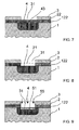
- First dopants of n conductivity type are implanted into the substrate 1 (shown by arrows 42 in FIG. 6 ) using the structured gate electrode layer 3 with its opening 31 as a mask, resulting in a first n doped implant region 41, the doping of the first implant region 41 being higher than the doping of the drift layer 12.
- the implanted first dopants are diffused into the substrate 1 (shown by arrows 43 in FIG. 7 ), resulting in an enhancement layer 4.
- Phosphorous or arsenic ions are preferably used as first dopants, preferably phosphorous ions.
- the first dopants are preferably implanted with an energy of 40-150 keV and / or a dose of 1 * 10 12 - 1 * 10 14 /cm 2 .
- the first dopants are driven in into the substrate 1 to a depth between 1 ⁇ m and 10 ⁇ m, in particular between 1 and 8 ⁇ m, and in particular between 1 and 6 ⁇ m.
- the first oxide layer 22 is partially removed in those areas, in which the opening 31 of the structured gate electrode layer 3 is arranged, typically by etching (shown by dotted line 21 in FIG. 8 ).
- seconds dopants of p conductivity type are implanted into the base region 5 (shown by arrows 55 in FIG. 9 ) using the structured oxide gate electrode layer 3 with its opening 31 as a mask, resulting in a second implant region 51.
- the implanted second dopants are diffused into the base region 5 (shown by arrows 52 in FIG. 10 ).
- the second dopants are preferably boron, aluminum, gallium or indium ions, preferably boron ions.
- the second dopants are preferably implanted with an energy of 20-120 keV and / or a dose of 5 * 10 13 - 3 * 10 14 /cm 2 .
- the second dopants are driven into a maximum depth 54 between 0.5 ⁇ m and 9 ⁇ m, in particular between 0.5 and 7 ⁇ m and in particular between 0.5 and 5 ⁇ m.
- the second dopants are driven into the substrate to a depth 53 in the central area (see FIG 1 ), which is less deep than the maximum depth 54 of the base region 5, which lies outside the central area and in the peripheral area, respectively.
- the second dopants are not only driven into the substrate 1 in a direction perpendicular to the surface, but they are spread out laterally, thus reducing the amount of second dopants in the central area.
- a depth 53 of the base region 5 in the central area of 1.6 ⁇ m was achieved, compared to a maximum depth 54 outside the central area of 2.4 ⁇ m.
- the energy used for the boron implantation is typically between 40 and 120 keV, in particular between 70 and 90 keV, in particular around 80 keV.
- a structured gate electrode layer 3 with at least two openings 31 and thus, to create at least two base regions 5, each surrounded by an enhancement layer 4.
- Highly (n+) doped source regions 6 and the layers on the collector side 121, namely the n doped buffer layer 9, the p doped collector layer 10 and the collector electrode 11 are manufactured at any appropriate manufacturing step and by any appropriate manufacturing method.
- the invention has been elaborated for planar semiconductors, but the inventive method can be applied also on trench gate semiconductors. Besides, the invention can also be applied to other semiconductor types like MOSFETs.
Landscapes
- Electrodes Of Semiconductors (AREA)
- Insulated Gate Type Field-Effect Transistor (AREA)
- Thyristors (AREA)
- Electrical Discharge Machining, Electrochemical Machining, And Combined Machining (AREA)
- Apparatuses And Processes For Manufacturing Resistors (AREA)
- Die Bonding (AREA)
- Junction Field-Effect Transistors (AREA)
Abstract
Description
- The invention relates to the field of power electronics and more particularly to a method for manufacturing a power semiconductor device according to the preamble of the independent claim.
- Prior art IGBTs have a low (n-) doped drift layer with a higher n doped buffer layer on the collector side followed by a collector layer. On the emitter side of the drift layer, which is opposite the collector side a p base layer is arranged. IGBTs have been improved by the introduction of an n doped enhancement layer, which is arranged between the p base layer and the (n-) drift layer and which separates these two layers. This leads to an IGBT with improved safe operating area (SOA) and low on-state losses. The carrier concentration near the active cell is enhanced by such an enhancement layer. In case of a metal-oxide semiconductor field-effect transistor (MOSFET), such an enhancement layer leads to a reduction of the junction field-effect transistor (JFET) effect and also to low on-state losses.
- If for an IGBT with an n enhancement layer as described above the p base layer has a higher depth at the edges of a cell compared to the central region of the cell, this profile for the pn-junction brings the peak field from the periphery of the cell to an area directly under the contact region of the emitter electrode. This position of the peak field results in a much higher SOA turn-off current capability for IGBTs as well as for MOSFETs and due to the fact that field generated holes can transport directly towards the contact region of the emitter electrode, a critical region near the n+ source regions is avoided which would result in the triggering of the parasitic thyristor and transistor for IGBTs and MOSFETs respectively.
-
EP 0 837 508 describes a method for manufacturing an insulated gate bipolar transistor (IGBT) with such a modulated p base layer profile. On a (p+) substrate first an n buffer layer and then a (n-) layer are formed by epitaxial growth. Afterwards, a thick gate oxide layer is formed on the (n-) layer and shaped in a designated pattern. Then a thin gate oxide layer is formed on top of the (n-) layer in areas, in which no thick oxide layer is formed, followed by a polysilicon layer on the gate oxide layers as a gate electrode. Then an open hole is formed in the thin gate oxide layer and the polysilicon layer. Phosphorous is implanted through the open hole into the (n-) layer and diffused into the (n-) layer, using the hole in the polysilicon layer as a mask, resulting in a first n layer. Afterwards, the hole is enlarged and phosphorous is again implanted and diffused, resulting in a second n layer. The depth of the first n layer is greater than the depth of the second n layer. Next, boron is implanted through the same mask of the polysilicon layer and diffused, resulting in a p layer, which is less deep than the second n layer. Thus, the second n layer and the p layer can be made by using the same mask, whereas for the manufacturing of the first n layer another mask is needed. - In an alternative, also described in
EP 0 837 508 the first n layer is produced after the second n layer, the second n layer being produced by a mask and implanting / diffusion as described above. After producing the second n layer, an insulation film is created on the gate electrode and structured by photoresist. The first n-layer can also be processed before the insulation film. For producing the first n layer high energy phosphorous ions are directly implanted from the open hole, which is limited by the photoresist and which is thus smaller than the hole used as a mask for the second n layer. The ions are directly implanted into the depth between the second n layer and the (n-) layer. The implant of high energy phosphorous ions is a complex process for depths exceeding 1 µm as required in the IGBT cell and the process also requires precise mask alignment in order to place the phosphorous in the middle of the cell. - It is an object of the invention to provide a method for the manufacturing of a power semiconductor device with low on-state losses and high SOA capability, which is easier to perform than the methods known from prior art and which thus avoids delicate manufacturing steps.
- This object is achieved by a method for manufacturing a power semiconductor device according to
claim 1. - The inventive method for manufacturing a power semiconductor device comprises the following steps:
- a first oxide layer is produced on a first main side of a substrate of a first conductivity type,
- a structured gate electrode layer with at least one opening is produced on the first main side on top of the first oxide layer,
- first dopants of the first conductivity type are implanted into the substrate on the first main side using the structured gate electrode layer as a mask,
- the first dopants are diffused into the substrate,
- second dopants of a second conductivity type are implanted into the substrate on the first main side and
- the second dopants are diffused into the substrate, characterized in that
- after diffusing the first dopants into the substrate and before implanting the second dopants into the substrate the first oxide layer is partially removed, resulting in a gate oxide layer, and in that
- the structured gate electrode layer is used as a mask for implanting the second dopants.
- The inventive method for manufacturing a power semiconductor device, in particular an IGBT or a MOSFET, has the advantage that one single mask is needed for the manufacturing of the base layer, made by the implant and diffusion of the first dopants of the first conductivity type, and the enhancement layer, made by the implant and diffusion of the second dopants of the second conductivity type. These layers are self-aligned by using the structured gate electrode layer as a mask.
- It has been surprisingly found out that due to the removal of the first oxide layer above the openings of the structured gate electrode layer after the diffusion of the first dopants and before the implant of the second dopants, a base layer of the second conductivity type is achieved, which has a lower depth in the central area below the contact area to the emitter electrode and a higher depth in the peripheral area of the base layer of the second conductivity type.
- Such a variation of the base layer profile allows operating the semiconductor device with low on-state losses and high SOA capability. The method is preferably used for the manufacturing of IGBTs and MOSFETs.
- The subject matter of the invention will be explained in more detail in the following text with reference to the attached drawings, in which:
- FIG 1
- shows an insulated gate semiconductor device according to the invention; and
- FIG 2-10
- show different steps of the method for manufacturing a semiconductor device according to the invention.
- The reference symbols used in the figures and their meaning are summarized in the list of reference symbols. Generally, alike or alike-functioning parts are given the same reference symbols. The described embodiments are meant as examples and shall not confine the invention.
- In
FIG 1 a power semiconductor device according to the invention is shown. An IGBT is shown with a low (n-) dopeddrift layer 12. Thedrift layer 12 has a first main side and a second main side, which is arranged opposite the first main side. The second main side is a collector side 121, on which an ndoped buffer layer 9, whichbuffer layer 9 has a higher doping than thedrift layer 12, is arranged. On thebuffer layer 9, on the side opposite the side, on which thedrift layer 12 is arranged, a p dopedcollector layer 10 and on top of thecollector layer 10, acollector electrode 11 is arranged. - On the first main side, which is an
emitter side 122 a p dopedbase region 5 is arranged, which is embedded in an n dopedenhancement layer 4. Theenhancement layer 4 has a higher doping than thedrift layer 12 and it separates thebase region 5 from thedrift layer 12. On the emitter side 122 agate oxide layer 2 is arranged, which is typically made of SiO2. Thegate oxide layer 2 is structured by an oxide opening, which leaves a part of the surface of thebase region 5 uncovered by thegate oxide layer 2. On top of the gate oxide layer 2 agate electrode layer 3, typically made of polysilicon, is arranged. Thegate electrode layer 3 has anopening 31 at the same location and, preferably, of the same size as theoxide layer 2. Thegate electrode layer 3 and thegate oxide layer 2 are covered by an insulation layer 7. Anemitter electrode 8 is afterwards arranged on top of the insulation layer 7 and in theopening 31 of thegate oxide layer 2 and thegate electrode layer 3 covered by the insulation layer 7. Within the p dopedbase region 5 highly (n+) doped source regions 6 are arranged, which are in contact with theemitter electrode 8 in the area of theopening 31 and extend at the surface of theemitter side 122 to a region underneath thegate electrode layer 3. - Typically, the
drift layer 12, thebase region 5, theenhancement region 4 and the source regions 6 form one common planar surface. - The
base region 5 has adepth 53 in the central area, which is lower than themaximum depth 54 of thebase region 5, which lies outside the central area, i.e. in the peripheral area of thebase region 5. - The inventive method for manufacturing a power semiconductor device is shown in the
FIGs. 2 to 10 . The method comprises manufacturing steps as follows. As shown inFIG. 2 the method is started with a lightly (n-)doped substrate 1, which has a collector side 121 (not shown in the figure) and anemitter side 122 opposite the collector side 121. As shown inFIG. 3 afirst oxide layer 22 completely covering thesubstrate 1 on theemitter side 122 is created. As shown inFIG. 4 an electricallyconductive layer 32 is produced on top of thefirst oxide layer 22. The electricallyconductive layer 32 covers thefirst oxide layer 22 completely. According toFIG. 5 anopening 31 in form of a through hole is etched in the electricallyconductive layer 32, resulting in a structuredgate electrode layer 3, so that part of the oxide layer 2' is now uncovered. - First dopants of n conductivity type are implanted into the substrate 1 (shown by
arrows 42 inFIG. 6 ) using the structuredgate electrode layer 3 with itsopening 31 as a mask, resulting in a first n dopedimplant region 41, the doping of thefirst implant region 41 being higher than the doping of thedrift layer 12. Afterwards, the implanted first dopants are diffused into the substrate 1 (shown byarrows 43 inFIG. 7 ), resulting in anenhancement layer 4. Phosphorous or arsenic ions are preferably used as first dopants, preferably phosphorous ions. The first dopants are preferably implanted with an energy of 40-150 keV and / or a dose of 1 * 1012 - 1 * 1014 /cm2. The first dopants are driven in into thesubstrate 1 to a depth between 1 µm and 10 µm, in particular between 1 and 8 µm, and in particular between 1 and 6 µm. - After creating the
enhancement layer 4, thefirst oxide layer 22 is partially removed in those areas, in which theopening 31 of the structuredgate electrode layer 3 is arranged, typically by etching (shown by dottedline 21 inFIG. 8 ). Afterwards, seconds dopants of p conductivity type are implanted into the base region 5 (shown byarrows 55 inFIG. 9 ) using the structured oxidegate electrode layer 3 with itsopening 31 as a mask, resulting in asecond implant region 51. Afterwards, the implanted second dopants are diffused into the base region 5 (shown byarrows 52 inFIG. 10 ). The second dopants are preferably boron, aluminum, gallium or indium ions, preferably boron ions. The second dopants are preferably implanted with an energy of 20-120 keV and / or a dose of 5 * 1013 - 3 * 1014 /cm2. The second dopants are driven into amaximum depth 54 between 0.5 µm and 9 µm, in particular between 0.5 and 7 µm and in particular between 0.5 and 5 µm. - Due to this manufacturing process the second dopants are driven into the substrate to a
depth 53 in the central area (seeFIG 1 ), which is less deep than themaximum depth 54 of thebase region 5, which lies outside the central area and in the peripheral area, respectively. As shown inFIG. 10 , the second dopants are not only driven into thesubstrate 1 in a direction perpendicular to the surface, but they are spread out laterally, thus reducing the amount of second dopants in the central area. For boron dopants, implanted with a low energy, adepth 53 of thebase region 5 in the central area of 1.6 µm was achieved, compared to amaximum depth 54 outside the central area of 2.4 µm. The energy used for the boron implantation is typically between 40 and 120 keV, in particular between 70 and 90 keV, in particular around 80 keV. - Of course, it is also possible to make a structured
gate electrode layer 3 with at least twoopenings 31 and thus, to create at least twobase regions 5, each surrounded by anenhancement layer 4. - Highly (n+) doped source regions 6 and the layers on the collector side 121, namely the n doped
buffer layer 9, the p dopedcollector layer 10 and thecollector electrode 11 are manufactured at any appropriate manufacturing step and by any appropriate manufacturing method. - It is possible to apply the invention to a method for the manufacturing of semiconductor devices, in which the conductivity type of all layers is reversed, i.e. with a lightly (p-) doped substrate etc.
- The invention has been elaborated for planar semiconductors, but the inventive method can be applied also on trench gate semiconductors. Besides, the invention can also be applied to other semiconductor types like MOSFETs.
-
- 1
- substrate
- 2
- gate oxide layer
- 21
- area
- 22
- first oxide layer
- 3
- gate electrode layer
- 32
- electrically conductive layer
- 31
- opening
- 4
- enhancement layer
- 41
- first implant region
- 41'
- implant of first dopants
- 42
- diffusion of first dopants
- 5
- base region
- 51
- second implant region
- 51'
- implant of second dopants
- 52
- diffusion of second dopants
- 53
- diffusion depth of second dopants in central area
- 54
- maximum diffusion depth of second dopants
- 6
- source region
- 7
- insulation layer
- 8
- emitter electrode
- 9
- buffer layer
- 10
- collector layer
- 11
- collector electrode
- 12
- drift layer
- 121
- collector side
- 122
- emitter sided
Claims (8)
- Method for manufacturing a power semiconductor device, which comprises the following manufacturing steps:a first oxide layer (22) is produced on a first main side of a substrate (1) of a first conductivity type,a gate electrode layer (3, 3') with at least one opening (31) is produced on the first main side on top of the first oxide layer (22), first dopants of the first conductivity type are implanted into the substrate (1) on the first main side using the gate electrode layer (3, 3') as a mask,the first dopants are diffused into the substrate (1),second dopants of a second conductivity type are implanted into the substrate (1) on the first main side andthe second dopants are diffused into the substrate (1), characterized in thatafter diffusing the first dopants into the substrate (1) and before implanting the second dopants into the substrate (1) the first oxide layer (22) is partially removed, and in thatthe gate electrode layer (3, 3') is used as a mask for implanting the second dopants.
- Method according to claim 1, characterized in that
the first oxide layer (22) is removed in those areas, in which the at least one opening (31) of the gate electrode layer (3, 3') is arranged, resulting in a gate oxide layer (2). - Method according to claim 1 or 2, characterized in that
the first dopants are phosphorous and/or arsenic ions. - Method according to any of the claims 1 to 3, characterized in that the first dopants are implanted with an energy of 40-150 keV and / or a dose of 1 * 1012-1 * 1014 /cm2.
- Method according to any of the claims 1 to 4, characterized in that the first dopants are diffused into the substrate (1) to a depth of at least 1 µm, and at maximum 10 µm, in particular 8 µm and in particular 6 µm.
- Method according to any of the claims 1 to 3, characterized in that the second dopants are boron, aluminum, gallium and/or indium ions.
- Method according to any of the claims 1 to 3, characterized in that the second dopants are implanted with an energy of 20-120 keV and / or a dose of 5 * 1013-3 * 1014 /cm2.
- Method according to any of the claims 1 to 3, characterized in that the second dopants are diffused into the substrate (1) to a maximum depth 54 of at least 0.5 µm and at maximum 9 µm, in particular 7 µm and in particular 5 µm.
Priority Applications (8)
| Application Number | Priority Date | Filing Date | Title |
|---|---|---|---|
| AT08171450T ATE507581T1 (en) | 2008-12-12 | 2008-12-12 | PRODUCTION PROCESS OF A POWER SEMICONDUCTOR COMPONENT |
| ES08171450T ES2364870T3 (en) | 2008-12-12 | 2008-12-12 | METHOD FOR THE MANUFACTURE OF AN ENERGY SEMICONDUCTOR DEVICE. |
| DE602008006579T DE602008006579D1 (en) | 2008-12-12 | 2008-12-12 | Manufacturing method of a power semiconductor device |
| EP08171450A EP2197025B1 (en) | 2008-12-12 | 2008-12-12 | Method for manufacturing a power semiconductor device |
| US12/635,975 US8324062B2 (en) | 2008-12-12 | 2009-12-11 | Method for manufacturing a power semiconductor device |
| RU2009146073/28A RU2510099C2 (en) | 2008-12-12 | 2009-12-11 | Method to manufacture power semiconductor device |
| JP2009282738A JP5791870B2 (en) | 2008-12-12 | 2009-12-14 | Method for manufacturing a semiconductor device |
| CN200910258365.3A CN101770949B (en) | 2008-12-12 | 2009-12-14 | Method for manufacturing a power semiconductor device |
Applications Claiming Priority (1)
| Application Number | Priority Date | Filing Date | Title |
|---|---|---|---|
| EP08171450A EP2197025B1 (en) | 2008-12-12 | 2008-12-12 | Method for manufacturing a power semiconductor device |
Publications (2)
| Publication Number | Publication Date |
|---|---|
| EP2197025A1 true EP2197025A1 (en) | 2010-06-16 |
| EP2197025B1 EP2197025B1 (en) | 2011-04-27 |
Family
ID=40352270
Family Applications (1)
| Application Number | Title | Priority Date | Filing Date |
|---|---|---|---|
| EP08171450A Active EP2197025B1 (en) | 2008-12-12 | 2008-12-12 | Method for manufacturing a power semiconductor device |
Country Status (8)
| Country | Link |
|---|---|
| US (1) | US8324062B2 (en) |
| EP (1) | EP2197025B1 (en) |
| JP (1) | JP5791870B2 (en) |
| CN (1) | CN101770949B (en) |
| AT (1) | ATE507581T1 (en) |
| DE (1) | DE602008006579D1 (en) |
| ES (1) | ES2364870T3 (en) |
| RU (1) | RU2510099C2 (en) |
Families Citing this family (5)
| Publication number | Priority date | Publication date | Assignee | Title |
|---|---|---|---|---|
| CN102934231B (en) * | 2010-06-17 | 2016-02-17 | Abb技术有限公司 | power semiconductor device |
| CN103839988A (en) * | 2012-11-23 | 2014-06-04 | 中国科学院微电子研究所 | Structure and Fabrication Method of EMPT-TI-IGBT Device |
| CN103839989A (en) * | 2012-11-23 | 2014-06-04 | 中国科学院微电子研究所 | A low-voltage IGBT with a buffer layer and its manufacturing method |
| CN103872115A (en) * | 2012-12-13 | 2014-06-18 | 中国科学院微电子研究所 | An enhanced micro punch-through IGBT |
| CN119947144B (en) * | 2025-01-23 | 2026-03-06 | 扬州国宇电子有限公司 | Insulated gate bipolar transistor and preparation method thereof |
Citations (3)
| Publication number | Priority date | Publication date | Assignee | Title |
|---|---|---|---|---|
| JPH03205832A (en) * | 1990-01-08 | 1991-09-09 | Hitachi Ltd | Insulated-gate semiconductor device and manufacture thereof |
| EP0837508A2 (en) | 1996-10-18 | 1998-04-22 | Hitachi, Ltd. | Semiconductor device and electric power conversion apparatus therewith |
| US20040065934A1 (en) * | 2002-08-27 | 2004-04-08 | International Rectifier Corp. | Bidirectional shallow trench superjunction device with resurf region |
Family Cites Families (17)
| Publication number | Priority date | Publication date | Assignee | Title |
|---|---|---|---|---|
| US3756861A (en) * | 1972-03-13 | 1973-09-04 | Bell Telephone Labor Inc | Bipolar transistors and method of manufacture |
| JPS57134855U (en) * | 1981-02-17 | 1982-08-23 | ||
| US5091336A (en) * | 1985-09-09 | 1992-02-25 | Harris Corporation | Method of making a high breakdown active device structure with low series resistance |
| EP0481153B1 (en) * | 1990-10-16 | 1997-02-12 | Consorzio per la Ricerca sulla Microelettronica nel Mezzogiorno - CoRiMMe | Process for the accomplishment of power MOS transistors with vertical current flow |
| EP0772242B1 (en) * | 1995-10-30 | 2006-04-05 | STMicroelectronics S.r.l. | Single feature size MOS technology power device |
| JPH10178174A (en) * | 1996-10-18 | 1998-06-30 | Hitachi Ltd | Semiconductor device and power conversion device using the same |
| US6121089A (en) * | 1997-10-17 | 2000-09-19 | Intersil Corporation | Methods of forming power semiconductor devices having merged split-well body regions therein |
| WO2000035021A1 (en) * | 1998-12-04 | 2000-06-15 | Infineon Technologies Ag | Power semiconductor switch |
| US6137139A (en) * | 1999-06-03 | 2000-10-24 | Intersil Corporation | Low voltage dual-well MOS device having high ruggedness, low on-resistance, and improved body diode reverse recovery |
| US20020179968A1 (en) * | 2001-05-30 | 2002-12-05 | Frank Pfirsch | Power semiconductor component, compensation component, power transistor, and method for producing power semiconductor components |
| JP3431909B2 (en) * | 2001-08-21 | 2003-07-28 | 沖電気工業株式会社 | LDMOS transistor manufacturing method |
| JP5134746B2 (en) * | 2001-09-20 | 2013-01-30 | 新電元工業株式会社 | Method for manufacturing field effect transistor |
| JP3914120B2 (en) * | 2002-09-04 | 2007-05-16 | 株式会社日立製作所 | Semiconductor device and power conversion device using the same |
| KR100512464B1 (en) * | 2002-12-30 | 2005-09-07 | 동부아남반도체 주식회사 | Fabricating method of electrically erasable and programmable read only memory device |
| US6965146B1 (en) * | 2004-11-29 | 2005-11-15 | Silicon-Based Technology Corp. | Self-aligned planar DMOS transistor structure and its manufacturing methods |
| US7351637B2 (en) * | 2006-04-10 | 2008-04-01 | General Electric Company | Semiconductor transistors having reduced channel widths and methods of fabricating same |
| RU2361318C2 (en) * | 2006-07-18 | 2009-07-10 | Федеральное Государственное Унитарное Предприятие "Научно-Производственное Предприятие "Пульсар" | Method of making power insulated-gate field-effect transistors |
-
2008
- 2008-12-12 EP EP08171450A patent/EP2197025B1/en active Active
- 2008-12-12 AT AT08171450T patent/ATE507581T1/en not_active IP Right Cessation
- 2008-12-12 DE DE602008006579T patent/DE602008006579D1/en active Active
- 2008-12-12 ES ES08171450T patent/ES2364870T3/en active Active
-
2009
- 2009-12-11 RU RU2009146073/28A patent/RU2510099C2/en active
- 2009-12-11 US US12/635,975 patent/US8324062B2/en active Active
- 2009-12-14 CN CN200910258365.3A patent/CN101770949B/en active Active
- 2009-12-14 JP JP2009282738A patent/JP5791870B2/en active Active
Patent Citations (3)
| Publication number | Priority date | Publication date | Assignee | Title |
|---|---|---|---|---|
| JPH03205832A (en) * | 1990-01-08 | 1991-09-09 | Hitachi Ltd | Insulated-gate semiconductor device and manufacture thereof |
| EP0837508A2 (en) | 1996-10-18 | 1998-04-22 | Hitachi, Ltd. | Semiconductor device and electric power conversion apparatus therewith |
| US20040065934A1 (en) * | 2002-08-27 | 2004-04-08 | International Rectifier Corp. | Bidirectional shallow trench superjunction device with resurf region |
Also Published As
| Publication number | Publication date |
|---|---|
| RU2510099C2 (en) | 2014-03-20 |
| CN101770949B (en) | 2014-11-19 |
| US20100151650A1 (en) | 2010-06-17 |
| JP5791870B2 (en) | 2015-10-07 |
| DE602008006579D1 (en) | 2011-06-09 |
| JP2010141339A (en) | 2010-06-24 |
| RU2009146073A (en) | 2011-06-20 |
| ES2364870T3 (en) | 2011-09-15 |
| ATE507581T1 (en) | 2011-05-15 |
| US8324062B2 (en) | 2012-12-04 |
| CN101770949A (en) | 2010-07-07 |
| EP2197025B1 (en) | 2011-04-27 |
Similar Documents
| Publication | Publication Date | Title |
|---|---|---|
| US20210098568A1 (en) | Power semiconductor devices having gate trenches and buried edge terminations and related methods | |
| US8592894B2 (en) | Method of forming a power semiconductor device and power semiconductor device | |
| EP1036411B1 (en) | Semiconductor power device manufacture | |
| JP4028482B2 (en) | Power MOSFET having trench gate electrode and manufacturing method thereof | |
| US6586800B2 (en) | Trench-gate semiconductor devices | |
| JP3652322B2 (en) | Vertical MOSFET and manufacturing method thereof | |
| EP2293336B1 (en) | Semiconductor device | |
| JP7775935B2 (en) | Semiconductor Devices | |
| US20040036138A1 (en) | High voltage power MOSFET having low on-resistance | |
| US20030022474A1 (en) | Manufacture of semiconductor devices with schottky barriers | |
| EP2061084A1 (en) | Reverse-conducting insulated gate bipolar transistor and corresponding manufacturing method | |
| JP2001284584A (en) | Semiconductor device and manufacturing method thereof | |
| JP4456013B2 (en) | Semiconductor device | |
| JP2005505921A (en) | Semiconductor power device having a floating island voltage sustaining layer | |
| CN110419111B (en) | Self-aligned and Robust Insulated Gate Bipolar Transistor Devices | |
| EP2197025B1 (en) | Method for manufacturing a power semiconductor device | |
| EP4336561A1 (en) | Insulated gate bipolar transistor with super junction structure, and preparation method therefor | |
| CN1589493A (en) | Method for forming trench MOSFET device with low parasitic resistance | |
| JPH08213620A (en) | Method for manufacturing semiconductor device controllable by field effect | |
| JP3792734B2 (en) | High voltage semiconductor element | |
| US20030060014A1 (en) | Field effect transistor configuration with high latch-up resistance, and method for its production | |
| EP2602826A1 (en) | Insulated gate power semiconductor device and method for manufacturing such a device | |
| CN115132575B (en) | Method for manufacturing semiconductor device | |
| KR20150003080A (en) | Power device and method for fabricating the same |
Legal Events
| Date | Code | Title | Description |
|---|---|---|---|
| PUAI | Public reference made under article 153(3) epc to a published international application that has entered the european phase |
Free format text: ORIGINAL CODE: 0009012 |
|
| 17P | Request for examination filed |
Effective date: 20091118 |
|
| AK | Designated contracting states |
Kind code of ref document: A1 Designated state(s): AT BE BG CH CY CZ DE DK EE ES FI FR GB GR HR HU IE IS IT LI LT LU LV MC MT NL NO PL PT RO SE SI SK TR |
|
| AX | Request for extension of the european patent |
Extension state: AL BA MK RS |
|
| GRAP | Despatch of communication of intention to grant a patent |
Free format text: ORIGINAL CODE: EPIDOSNIGR1 |
|
| AKX | Designation fees paid |
Designated state(s): AT BE BG CH CY CZ DE DK EE ES FI FR GB GR HR HU IE IS IT LI LT LU LV MC MT NL NO PL PT RO SE SI SK TR |
|
| GRAS | Grant fee paid |
Free format text: ORIGINAL CODE: EPIDOSNIGR3 |
|
| GRAA | (expected) grant |
Free format text: ORIGINAL CODE: 0009210 |
|
| AK | Designated contracting states |
Kind code of ref document: B1 Designated state(s): AT BE BG CH CY CZ DE DK EE ES FI FR GB GR HR HU IE IS IT LI LT LU LV MC MT NL NO PL PT RO SE SI SK TR |
|
| REG | Reference to a national code |
Ref country code: GB Ref legal event code: FG4D |
|
| REG | Reference to a national code |
Ref country code: CH Ref legal event code: EP |
|
| REG | Reference to a national code |
Ref country code: IE Ref legal event code: FG4D |
|
| REF | Corresponds to: |
Ref document number: 602008006579 Country of ref document: DE Date of ref document: 20110609 Kind code of ref document: P |
|
| REG | Reference to a national code |
Ref country code: DE Ref legal event code: R096 Ref document number: 602008006579 Country of ref document: DE Effective date: 20110609 |
|
| REG | Reference to a national code |
Ref country code: CH Ref legal event code: NV Representative=s name: ABB SCHWEIZ AG INTELLECTUAL PROPERTY (CH-LC/IP) |
|
| REG | Reference to a national code |
Ref country code: NL Ref legal event code: VDEP Effective date: 20110427 |
|
| REG | Reference to a national code |
Ref country code: ES Ref legal event code: FG2A Ref document number: 2364870 Country of ref document: ES Kind code of ref document: T3 Effective date: 20110915 |
|
| LTIE | Lt: invalidation of european patent or patent extension |
Effective date: 20110427 |
|
| PG25 | Lapsed in a contracting state [announced via postgrant information from national office to epo] |
Ref country code: SE Free format text: LAPSE BECAUSE OF FAILURE TO SUBMIT A TRANSLATION OF THE DESCRIPTION OR TO PAY THE FEE WITHIN THE PRESCRIBED TIME-LIMIT Effective date: 20110427 Ref country code: NO Free format text: LAPSE BECAUSE OF FAILURE TO SUBMIT A TRANSLATION OF THE DESCRIPTION OR TO PAY THE FEE WITHIN THE PRESCRIBED TIME-LIMIT Effective date: 20110727 Ref country code: HR Free format text: LAPSE BECAUSE OF FAILURE TO SUBMIT A TRANSLATION OF THE DESCRIPTION OR TO PAY THE FEE WITHIN THE PRESCRIBED TIME-LIMIT Effective date: 20110427 Ref country code: LT Free format text: LAPSE BECAUSE OF FAILURE TO SUBMIT A TRANSLATION OF THE DESCRIPTION OR TO PAY THE FEE WITHIN THE PRESCRIBED TIME-LIMIT Effective date: 20110427 Ref country code: PT Free format text: LAPSE BECAUSE OF FAILURE TO SUBMIT A TRANSLATION OF THE DESCRIPTION OR TO PAY THE FEE WITHIN THE PRESCRIBED TIME-LIMIT Effective date: 20110829 |
|
| PG25 | Lapsed in a contracting state [announced via postgrant information from national office to epo] |
Ref country code: IS Free format text: LAPSE BECAUSE OF FAILURE TO SUBMIT A TRANSLATION OF THE DESCRIPTION OR TO PAY THE FEE WITHIN THE PRESCRIBED TIME-LIMIT Effective date: 20110827 Ref country code: SI Free format text: LAPSE BECAUSE OF FAILURE TO SUBMIT A TRANSLATION OF THE DESCRIPTION OR TO PAY THE FEE WITHIN THE PRESCRIBED TIME-LIMIT Effective date: 20110427 Ref country code: BE Free format text: LAPSE BECAUSE OF FAILURE TO SUBMIT A TRANSLATION OF THE DESCRIPTION OR TO PAY THE FEE WITHIN THE PRESCRIBED TIME-LIMIT Effective date: 20110427 Ref country code: LV Free format text: LAPSE BECAUSE OF FAILURE TO SUBMIT A TRANSLATION OF THE DESCRIPTION OR TO PAY THE FEE WITHIN THE PRESCRIBED TIME-LIMIT Effective date: 20110427 Ref country code: CY Free format text: LAPSE BECAUSE OF FAILURE TO SUBMIT A TRANSLATION OF THE DESCRIPTION OR TO PAY THE FEE WITHIN THE PRESCRIBED TIME-LIMIT Effective date: 20110427 Ref country code: FI Free format text: LAPSE BECAUSE OF FAILURE TO SUBMIT A TRANSLATION OF THE DESCRIPTION OR TO PAY THE FEE WITHIN THE PRESCRIBED TIME-LIMIT Effective date: 20110427 Ref country code: AT Free format text: LAPSE BECAUSE OF FAILURE TO SUBMIT A TRANSLATION OF THE DESCRIPTION OR TO PAY THE FEE WITHIN THE PRESCRIBED TIME-LIMIT Effective date: 20110427 Ref country code: GR Free format text: LAPSE BECAUSE OF FAILURE TO SUBMIT A TRANSLATION OF THE DESCRIPTION OR TO PAY THE FEE WITHIN THE PRESCRIBED TIME-LIMIT Effective date: 20110728 |
|
| PG25 | Lapsed in a contracting state [announced via postgrant information from national office to epo] |
Ref country code: NL Free format text: LAPSE BECAUSE OF FAILURE TO SUBMIT A TRANSLATION OF THE DESCRIPTION OR TO PAY THE FEE WITHIN THE PRESCRIBED TIME-LIMIT Effective date: 20110427 |
|
| PG25 | Lapsed in a contracting state [announced via postgrant information from national office to epo] |
Ref country code: CZ Free format text: LAPSE BECAUSE OF FAILURE TO SUBMIT A TRANSLATION OF THE DESCRIPTION OR TO PAY THE FEE WITHIN THE PRESCRIBED TIME-LIMIT Effective date: 20110427 Ref country code: EE Free format text: LAPSE BECAUSE OF FAILURE TO SUBMIT A TRANSLATION OF THE DESCRIPTION OR TO PAY THE FEE WITHIN THE PRESCRIBED TIME-LIMIT Effective date: 20110427 |
|
| PG25 | Lapsed in a contracting state [announced via postgrant information from national office to epo] |
Ref country code: DK Free format text: LAPSE BECAUSE OF FAILURE TO SUBMIT A TRANSLATION OF THE DESCRIPTION OR TO PAY THE FEE WITHIN THE PRESCRIBED TIME-LIMIT Effective date: 20110427 Ref country code: SK Free format text: LAPSE BECAUSE OF FAILURE TO SUBMIT A TRANSLATION OF THE DESCRIPTION OR TO PAY THE FEE WITHIN THE PRESCRIBED TIME-LIMIT Effective date: 20110427 Ref country code: RO Free format text: LAPSE BECAUSE OF FAILURE TO SUBMIT A TRANSLATION OF THE DESCRIPTION OR TO PAY THE FEE WITHIN THE PRESCRIBED TIME-LIMIT Effective date: 20110427 Ref country code: PL Free format text: LAPSE BECAUSE OF FAILURE TO SUBMIT A TRANSLATION OF THE DESCRIPTION OR TO PAY THE FEE WITHIN THE PRESCRIBED TIME-LIMIT Effective date: 20110427 |
|
| PLBE | No opposition filed within time limit |
Free format text: ORIGINAL CODE: 0009261 |
|
| STAA | Information on the status of an ep patent application or granted ep patent |
Free format text: STATUS: NO OPPOSITION FILED WITHIN TIME LIMIT |
|
| 26N | No opposition filed |
Effective date: 20120130 |
|
| REG | Reference to a national code |
Ref country code: DE Ref legal event code: R097 Ref document number: 602008006579 Country of ref document: DE Effective date: 20120130 |
|
| PG25 | Lapsed in a contracting state [announced via postgrant information from national office to epo] |
Ref country code: IT Free format text: LAPSE BECAUSE OF FAILURE TO SUBMIT A TRANSLATION OF THE DESCRIPTION OR TO PAY THE FEE WITHIN THE PRESCRIBED TIME-LIMIT Effective date: 20110427 |
|
| PG25 | Lapsed in a contracting state [announced via postgrant information from national office to epo] |
Ref country code: MC Free format text: LAPSE BECAUSE OF NON-PAYMENT OF DUE FEES Effective date: 20111231 |
|
| REG | Reference to a national code |
Ref country code: IE Ref legal event code: MM4A |
|
| PG25 | Lapsed in a contracting state [announced via postgrant information from national office to epo] |
Ref country code: IE Free format text: LAPSE BECAUSE OF NON-PAYMENT OF DUE FEES Effective date: 20111212 |
|
| PG25 | Lapsed in a contracting state [announced via postgrant information from national office to epo] |
Ref country code: MT Free format text: LAPSE BECAUSE OF FAILURE TO SUBMIT A TRANSLATION OF THE DESCRIPTION OR TO PAY THE FEE WITHIN THE PRESCRIBED TIME-LIMIT Effective date: 20110427 |
|
| PG25 | Lapsed in a contracting state [announced via postgrant information from national office to epo] |
Ref country code: LU Free format text: LAPSE BECAUSE OF NON-PAYMENT OF DUE FEES Effective date: 20111212 |
|
| PG25 | Lapsed in a contracting state [announced via postgrant information from national office to epo] |
Ref country code: BG Free format text: LAPSE BECAUSE OF FAILURE TO SUBMIT A TRANSLATION OF THE DESCRIPTION OR TO PAY THE FEE WITHIN THE PRESCRIBED TIME-LIMIT Effective date: 20110727 |
|
| PG25 | Lapsed in a contracting state [announced via postgrant information from national office to epo] |
Ref country code: TR Free format text: LAPSE BECAUSE OF FAILURE TO SUBMIT A TRANSLATION OF THE DESCRIPTION OR TO PAY THE FEE WITHIN THE PRESCRIBED TIME-LIMIT Effective date: 20110427 |
|
| PG25 | Lapsed in a contracting state [announced via postgrant information from national office to epo] |
Ref country code: HU Free format text: LAPSE BECAUSE OF FAILURE TO SUBMIT A TRANSLATION OF THE DESCRIPTION OR TO PAY THE FEE WITHIN THE PRESCRIBED TIME-LIMIT Effective date: 20110427 |
|
| REG | Reference to a national code |
Ref country code: FR Ref legal event code: PLFP Year of fee payment: 8 |
|
| REG | Reference to a national code |
Ref country code: FR Ref legal event code: PLFP Year of fee payment: 9 |
|
| REG | Reference to a national code |
Ref country code: DE Ref legal event code: R081 Ref document number: 602008006579 Country of ref document: DE Owner name: HITACHI ENERGY SWITZERLAND AG, CH Free format text: FORMER OWNER: ABB TECHNOLOGY AG, ZUERICH, CH Ref country code: DE Ref legal event code: R081 Ref document number: 602008006579 Country of ref document: DE Owner name: ABB SCHWEIZ AG, CH Free format text: FORMER OWNER: ABB TECHNOLOGY AG, ZUERICH, CH Ref country code: DE Ref legal event code: R081 Ref document number: 602008006579 Country of ref document: DE Owner name: ABB POWER GRIDS SWITZERLAND AG, CH Free format text: FORMER OWNER: ABB TECHNOLOGY AG, ZUERICH, CH Ref country code: DE Ref legal event code: R082 Ref document number: 602008006579 Country of ref document: DE Representative=s name: DENNEMEYER & ASSOCIATES S.A., DE Ref country code: DE Ref legal event code: R082 Ref document number: 602008006579 Country of ref document: DE Representative=s name: ZIMMERMANN & PARTNER PATENTANWAELTE MBB, DE |
|
| REG | Reference to a national code |
Ref country code: FR Ref legal event code: PLFP Year of fee payment: 10 |
|
| REG | Reference to a national code |
Ref country code: ES Ref legal event code: PC2A Owner name: ABB SCHWEIZ AG Effective date: 20171218 |
|
| REG | Reference to a national code |
Ref country code: CH Ref legal event code: PFUS Owner name: ABB SCHWEIZ AG, CH Free format text: FORMER OWNER: ABB TECHNOLOGY AG, CH |
|
| REG | Reference to a national code |
Ref country code: GB Ref legal event code: 732E Free format text: REGISTERED BETWEEN 20180426 AND 20180502 |
|
| REG | Reference to a national code |
Ref country code: FR Ref legal event code: TP Owner name: ABB SCHWEIZ AG, CH Effective date: 20180912 |
|
| REG | Reference to a national code |
Ref country code: CH Ref legal event code: PUE Owner name: ABB POWER GRIDS SWITZERLAND AG, CH Free format text: FORMER OWNER: ABB SCHWEIZ AG, CH |
|
| REG | Reference to a national code |
Ref country code: DE Ref legal event code: R081 Ref document number: 602008006579 Country of ref document: DE Owner name: HITACHI ENERGY SWITZERLAND AG, CH Free format text: FORMER OWNER: ABB SCHWEIZ AG, BADEN, CH Ref country code: DE Ref legal event code: R082 Ref document number: 602008006579 Country of ref document: DE Representative=s name: DENNEMEYER & ASSOCIATES RECHTSANWALTSGESELLSCH, DE Ref country code: DE Ref legal event code: R081 Ref document number: 602008006579 Country of ref document: DE Owner name: HITACHI ENERGY LTD, CH Free format text: FORMER OWNER: ABB SCHWEIZ AG, BADEN, CH Ref country code: DE Ref legal event code: R082 Ref document number: 602008006579 Country of ref document: DE Representative=s name: DENNEMEYER & ASSOCIATES S.A., DE Ref country code: DE Ref legal event code: R081 Ref document number: 602008006579 Country of ref document: DE Owner name: ABB POWER GRIDS SWITZERLAND AG, CH Free format text: FORMER OWNER: ABB SCHWEIZ AG, BADEN, CH |
|
| REG | Reference to a national code |
Ref country code: ES Ref legal event code: PC2A Owner name: ABB POWER GRIDS SWITZERLAND AG Effective date: 20210520 |
|
| REG | Reference to a national code |
Ref country code: GB Ref legal event code: 732E Free format text: REGISTERED BETWEEN 20210909 AND 20210915 |
|
| REG | Reference to a national code |
Ref country code: ES Ref legal event code: PC2A Owner name: HITACHI ENERGY SWITZERLAND AG Effective date: 20220526 |
|
| REG | Reference to a national code |
Ref country code: DE Ref legal event code: R081 Ref document number: 602008006579 Country of ref document: DE Owner name: HITACHI ENERGY SWITZERLAND AG, CH Free format text: FORMER OWNER: ABB POWER GRIDS SWITZERLAND AG, BADEN, CH Ref country code: DE Ref legal event code: R081 Ref document number: 602008006579 Country of ref document: DE Owner name: HITACHI ENERGY LTD, CH Free format text: FORMER OWNER: ABB POWER GRIDS SWITZERLAND AG, BADEN, CH |
|
| P01 | Opt-out of the competence of the unified patent court (upc) registered |
Effective date: 20230527 |
|
| REG | Reference to a national code |
Ref country code: DE Ref legal event code: R082 Ref document number: 602008006579 Country of ref document: DE Representative=s name: DENNEMEYER & ASSOCIATES RECHTSANWALTSGESELLSCH, DE Ref country code: DE Ref legal event code: R082 Ref document number: 602008006579 Country of ref document: DE Representative=s name: DENNEMEYER & ASSOCIATES S.A., DE Ref country code: DE Ref legal event code: R081 Ref document number: 602008006579 Country of ref document: DE Owner name: HITACHI ENERGY LTD, CH Free format text: FORMER OWNER: HITACHI ENERGY SWITZERLAND AG, BADEN, CH |
|
| REG | Reference to a national code |
Ref country code: GB Ref legal event code: 732E Free format text: REGISTERED BETWEEN 20240718 AND 20240724 |
|
| REG | Reference to a national code |
Ref country code: ES Ref legal event code: PC2A Owner name: HITACHI ENERGY LTD Effective date: 20240925 |
|
| REG | Reference to a national code |
Ref country code: DE Ref legal event code: R079 Ref document number: 602008006579 Country of ref document: DE Free format text: PREVIOUS MAIN CLASS: H01L0021331000 Ipc: H10D0012010000 |
|
| REG | Reference to a national code |
Ref country code: DE Ref legal event code: R082 Ref document number: 602008006579 Country of ref document: DE Representative=s name: DENNEMEYER & ASSOCIATES RECHTSANWALTSGESELLSCH, DE |
|
| REG | Reference to a national code |
Ref country code: CH Ref legal event code: U11 Free format text: ST27 STATUS EVENT CODE: U-0-0-U10-U11 (AS PROVIDED BY THE NATIONAL OFFICE) Effective date: 20260101 |
|
| PGFP | Annual fee paid to national office [announced via postgrant information from national office to epo] |
Ref country code: DE Payment date: 20251211 Year of fee payment: 18 |
|
| PGFP | Annual fee paid to national office [announced via postgrant information from national office to epo] |
Ref country code: GB Payment date: 20251219 Year of fee payment: 18 |
|
| PGFP | Annual fee paid to national office [announced via postgrant information from national office to epo] |
Ref country code: FR Payment date: 20251222 Year of fee payment: 18 |
|
| PGFP | Annual fee paid to national office [announced via postgrant information from national office to epo] |
Ref country code: ES Payment date: 20260130 Year of fee payment: 18 |
|
| PGFP | Annual fee paid to national office [announced via postgrant information from national office to epo] |
Ref country code: CH Payment date: 20260101 Year of fee payment: 18 |