EP2192643A2 - Electrode plate multi-end sides to single end side current collector of an electricity storage/discharge device - Google Patents
Electrode plate multi-end sides to single end side current collector of an electricity storage/discharge device Download PDFInfo
- Publication number
- EP2192643A2 EP2192643A2 EP09252714A EP09252714A EP2192643A2 EP 2192643 A2 EP2192643 A2 EP 2192643A2 EP 09252714 A EP09252714 A EP 09252714A EP 09252714 A EP09252714 A EP 09252714A EP 2192643 A2 EP2192643 A2 EP 2192643A2
- Authority
- EP
- European Patent Office
- Prior art keywords
- electrode plate
- current collecting
- sides
- electric conductor
- input
- Prior art date
- Legal status (The legal status is an assumption and is not a legal conclusion. Google has not performed a legal analysis and makes no representation as to the accuracy of the status listed.)
- Granted
Links
- 230000005611 electricity Effects 0.000 title claims description 76
- 239000004020 conductor Substances 0.000 claims abstract description 216
- 239000012212 insulator Substances 0.000 claims abstract description 87
- 230000005540 biological transmission Effects 0.000 claims description 20
- 239000003990 capacitor Substances 0.000 claims description 16
- 230000002708 enhancing effect Effects 0.000 claims description 14
- 238000000034 method Methods 0.000 claims description 13
- 239000000446 fuel Substances 0.000 claims description 7
- 239000012774 insulation material Substances 0.000 claims description 7
- 230000002349 favourable effect Effects 0.000 claims description 4
- 239000011888 foil Substances 0.000 claims description 4
- 230000004927 fusion Effects 0.000 claims description 4
- 238000003466 welding Methods 0.000 claims description 4
- 238000009434 installation Methods 0.000 claims description 2
- 238000009413 insulation Methods 0.000 claims description 2
- 239000000463 material Substances 0.000 claims description 2
- 230000000750 progressive effect Effects 0.000 description 1
Images


Classifications
-
- H—ELECTRICITY
- H01—ELECTRIC ELEMENTS
- H01M—PROCESSES OR MEANS, e.g. BATTERIES, FOR THE DIRECT CONVERSION OF CHEMICAL ENERGY INTO ELECTRICAL ENERGY
- H01M50/00—Constructional details or processes of manufacture of the non-active parts of electrochemical cells other than fuel cells, e.g. hybrid cells
- H01M50/50—Current conducting connections for cells or batteries
- H01M50/543—Terminals
-
- H—ELECTRICITY
- H01—ELECTRIC ELEMENTS
- H01G—CAPACITORS; CAPACITORS, RECTIFIERS, DETECTORS, SWITCHING DEVICES OR LIGHT-SENSITIVE DEVICES, OF THE ELECTROLYTIC TYPE
- H01G11/00—Hybrid capacitors, i.e. capacitors having different positive and negative electrodes; Electric double-layer [EDL] capacitors; Processes for the manufacture thereof or of parts thereof
- H01G11/66—Current collectors
- H01G11/72—Current collectors specially adapted for integration in multiple or stacked hybrid or EDL capacitors
-
- H—ELECTRICITY
- H01—ELECTRIC ELEMENTS
- H01G—CAPACITORS; CAPACITORS, RECTIFIERS, DETECTORS, SWITCHING DEVICES OR LIGHT-SENSITIVE DEVICES, OF THE ELECTROLYTIC TYPE
- H01G11/00—Hybrid capacitors, i.e. capacitors having different positive and negative electrodes; Electric double-layer [EDL] capacitors; Processes for the manufacture thereof or of parts thereof
- H01G11/74—Terminals, e.g. extensions of current collectors
-
- H—ELECTRICITY
- H01—ELECTRIC ELEMENTS
- H01G—CAPACITORS; CAPACITORS, RECTIFIERS, DETECTORS, SWITCHING DEVICES OR LIGHT-SENSITIVE DEVICES, OF THE ELECTROLYTIC TYPE
- H01G11/00—Hybrid capacitors, i.e. capacitors having different positive and negative electrodes; Electric double-layer [EDL] capacitors; Processes for the manufacture thereof or of parts thereof
- H01G11/78—Cases; Housings; Encapsulations; Mountings
- H01G11/82—Fixing or assembling a capacitive element in a housing, e.g. mounting electrodes, current collectors or terminals in containers or encapsulations
-
- H—ELECTRICITY
- H01—ELECTRIC ELEMENTS
- H01M—PROCESSES OR MEANS, e.g. BATTERIES, FOR THE DIRECT CONVERSION OF CHEMICAL ENERGY INTO ELECTRICAL ENERGY
- H01M4/00—Electrodes
- H01M4/02—Electrodes composed of, or comprising, active material
- H01M4/64—Carriers or collectors
- H01M4/66—Selection of materials
- H01M4/665—Composites
- H01M4/667—Composites in the form of layers, e.g. coatings
-
- H—ELECTRICITY
- H01—ELECTRIC ELEMENTS
- H01M—PROCESSES OR MEANS, e.g. BATTERIES, FOR THE DIRECT CONVERSION OF CHEMICAL ENERGY INTO ELECTRICAL ENERGY
- H01M4/00—Electrodes
- H01M4/02—Electrodes composed of, or comprising, active material
- H01M4/64—Carriers or collectors
- H01M4/70—Carriers or collectors characterised by shape or form
-
- H—ELECTRICITY
- H01—ELECTRIC ELEMENTS
- H01M—PROCESSES OR MEANS, e.g. BATTERIES, FOR THE DIRECT CONVERSION OF CHEMICAL ENERGY INTO ELECTRICAL ENERGY
- H01M50/00—Constructional details or processes of manufacture of the non-active parts of electrochemical cells other than fuel cells, e.g. hybrid cells
- H01M50/50—Current conducting connections for cells or batteries
- H01M50/531—Electrode connections inside a battery casing
- H01M50/533—Electrode connections inside a battery casing characterised by the shape of the leads or tabs
-
- H—ELECTRICITY
- H01—ELECTRIC ELEMENTS
- H01M—PROCESSES OR MEANS, e.g. BATTERIES, FOR THE DIRECT CONVERSION OF CHEMICAL ENERGY INTO ELECTRICAL ENERGY
- H01M50/00—Constructional details or processes of manufacture of the non-active parts of electrochemical cells other than fuel cells, e.g. hybrid cells
- H01M50/50—Current conducting connections for cells or batteries
- H01M50/543—Terminals
- H01M50/547—Terminals characterised by the disposition of the terminals on the cells
- H01M50/55—Terminals characterised by the disposition of the terminals on the cells on the same side of the cell
-
- H—ELECTRICITY
- H01—ELECTRIC ELEMENTS
- H01M—PROCESSES OR MEANS, e.g. BATTERIES, FOR THE DIRECT CONVERSION OF CHEMICAL ENERGY INTO ELECTRICAL ENERGY
- H01M8/00—Fuel cells; Manufacture thereof
- H01M8/02—Details
- H01M8/0202—Collectors; Separators, e.g. bipolar separators; Interconnectors
- H01M8/0247—Collectors; Separators, e.g. bipolar separators; Interconnectors characterised by the form
-
- Y—GENERAL TAGGING OF NEW TECHNOLOGICAL DEVELOPMENTS; GENERAL TAGGING OF CROSS-SECTIONAL TECHNOLOGIES SPANNING OVER SEVERAL SECTIONS OF THE IPC; TECHNICAL SUBJECTS COVERED BY FORMER USPC CROSS-REFERENCE ART COLLECTIONS [XRACs] AND DIGESTS
- Y02—TECHNOLOGIES OR APPLICATIONS FOR MITIGATION OR ADAPTATION AGAINST CLIMATE CHANGE
- Y02E—REDUCTION OF GREENHOUSE GAS [GHG] EMISSIONS, RELATED TO ENERGY GENERATION, TRANSMISSION OR DISTRIBUTION
- Y02E60/00—Enabling technologies; Technologies with a potential or indirect contribution to GHG emissions mitigation
- Y02E60/10—Energy storage using batteries
-
- Y—GENERAL TAGGING OF NEW TECHNOLOGICAL DEVELOPMENTS; GENERAL TAGGING OF CROSS-SECTIONAL TECHNOLOGIES SPANNING OVER SEVERAL SECTIONS OF THE IPC; TECHNICAL SUBJECTS COVERED BY FORMER USPC CROSS-REFERENCE ART COLLECTIONS [XRACs] AND DIGESTS
- Y02—TECHNOLOGIES OR APPLICATIONS FOR MITIGATION OR ADAPTATION AGAINST CLIMATE CHANGE
- Y02E—REDUCTION OF GREENHOUSE GAS [GHG] EMISSIONS, RELATED TO ENERGY GENERATION, TRANSMISSION OR DISTRIBUTION
- Y02E60/00—Enabling technologies; Technologies with a potential or indirect contribution to GHG emissions mitigation
- Y02E60/13—Energy storage using capacitors
-
- Y—GENERAL TAGGING OF NEW TECHNOLOGICAL DEVELOPMENTS; GENERAL TAGGING OF CROSS-SECTIONAL TECHNOLOGIES SPANNING OVER SEVERAL SECTIONS OF THE IPC; TECHNICAL SUBJECTS COVERED BY FORMER USPC CROSS-REFERENCE ART COLLECTIONS [XRACs] AND DIGESTS
- Y02—TECHNOLOGIES OR APPLICATIONS FOR MITIGATION OR ADAPTATION AGAINST CLIMATE CHANGE
- Y02E—REDUCTION OF GREENHOUSE GAS [GHG] EMISSIONS, RELATED TO ENERGY GENERATION, TRANSMISSION OR DISTRIBUTION
- Y02E60/00—Enabling technologies; Technologies with a potential or indirect contribution to GHG emissions mitigation
- Y02E60/30—Hydrogen technology
- Y02E60/50—Fuel cells
Definitions
- the present invention discloses an improved multi-end sides to single end side input/output current collecting terminal structure being applied to the electrode plate of an electricity storage/discharge device for applications in electricity storage/discharge devices such as primary batteries, secondary chargeable/dischargeable batteries, capacitors, or super-capacitors, or fuel cell power supply device having electrode plates, wherein two or more than two end sides of each electrode plate of above said device are made with one or more than one current collecting terminal structure thereby allowing the electrode plate via multiple current collecting terminals on multi-sides to collect currents in multi-circuits, wherein the auxiliary electric conductor is additionally installed between the positive or negative electrode plate installed on end-side of individual electrode cell and the electrode cell casing, and the insulator is installed between the electrode plate and the auxiliary electric conductor thereby allowing current collecting terminals at different end-sides of the electrode plates in the same polarity to be connected via the auxiliary electric conductors to collect the currents of current collecting terminals at multiple end sides to the current collecting terminal at single end side to facilitate collecting
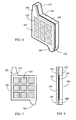
- FIG. 1 is a schematic view showing the embodiment of the conventional electrode plate being made with one current collecting terminal on one end-side thereof, wherein one single end side of each electrode plate (P100) is made with a current collecting terminal (T100) to provide current collecting function for input or output current of the electrode plate, or to be used as the connection point for series connection or parallel connection with other electrode plates, however, as the electrode plate is only made with one current collecting terminal at the single end side thereof for output or input current, the current density of the electrode plate in case of large input or output current appears disproportionate phenomenon at the another end side of electrode plate and area farther away from current collecting terminal (T100) on the electrode plate; the more progressive one is that the electrode plate is made with two and more than two current collecting terminals on the same end side thereof thereby allowing the electrode plate to have two or more
- the electrode plate is improved by installing one or more than one individually outwardly extended current collecting terminal on the two or more than two end sides thereof, such as that Fig. 2 is a schematic view showing the embodiment of the electrode plate being made with a current collecting terminal respectively at two end-sides thereof; or one or more than one end side of the electrode plate (P100) is made with two or more than two current collecting terminals (T100) to constitute two or more than two input or output current paths thereby lowering internal resistances, such as that Fig. 3 shows an electrode plate being made with two current collecting terminals respectively at the two opposite end-sides; however, although input/output current uniformity is improved by the methods shown in Fig. 2 and Fig. 3 , the external input/output terminals installed on the two end sides are still inconvenient for use.
- Two or more than two end sides of the electrode plates applied in the electricity storage/discharge device are made with one or more than one current collecting terminal structure thereby allowing the electrode plate via multiple current collecting terminals on multi-sides to collect currents in multi-circuits, wherein the auxiliary electric conductor is additionally installed between the positive or negative electrode plate installed on end-side of the individual electrode cell and the electrode cell casing, and the insulator is installed between the electrode plate and the auxiliary electric conductor thereby allowing current collecting terminals at different end-sides of the electrode plates in the same polarity to be connected via the auxiliary electric conductors to collect the currents of current collecting terminals at multiple end sides to the current collecting terminal at single end side to facilitate collecting input/output currents to the outside, wherein the number of external input/output current collecting terminals on the single end side of electrode plate can be one more than one.
- the present invention discloses an improved multi-end sides to single end side input/output current collecting terminal structure being applied to the electrode plate of an electricity storage/discharge device for applications in electricity storage/discharge devices such as primary batteries, secondary chargeable/dischargeable batteries, capacitors, or super-capacitors, or fuel cell power supply device having electrode plates, wherein two or more than two end sides of each electrode plate of above said device are made with one or more than one current collecting terminal structure thereby allowing the electrode plate via multiple current collecting terminals on multi-sides to collect currents in multi-circuits, wherein the auxiliary electric conductor is additionally installed between the positive or negative electrode plate installed on end-side of individual electrode cell and the electrode cell casing, and the insulator is installed between the electrode plate and the auxiliary electric conductor thereby allowing current collecting terminals at different end-sides of the electrode plates in the same polarity to be connected via the auxiliary electric conductors to collect the currents of current collecting terminals at multiple end sides to the current collecting terminal at single end side to facilitate collecting
- the main constitution characteristics of the electrode plate multi-end sides to single end side current collector of an electricity storage/discharge device of the present invention are as following:
- the installation methods of the insulators interposed between the side electrode plate of the end-side of the electrode cell and the auxiliary electric conductor can be constituted by one or more than one method as following, include:
- the electrode plate multi-end sides to single end side current collector of an electricity storage/discharge device of the present invention is further made by connecting electric conductors to connect the current collecting terminals of the individual electrode plates in the same voltage and the same polarity installed inside the same or different electrode cells for parallel connection, or to connect the current collecting terminals of electrode plates in opposite polarities installed inside different electrode cells for series connection or mixed series and parallel connection;
- the constitution characteristics include:
- the insulator (103) is interposed between aforesaid side electrode plate (101) and auxiliary electric conductor (100) which are parallel connected via current collecting terminals (104, 106) for electric conduction and are through the parallel connection between the input/output current collecting terminals (105, 106) for electric conduction thereby constituting the input/output current collecting function for common input or output currents to the outside.
- said current collecting terminals (104, 106) on the other end thereof not arranged for common input/output currents to the outside can also be not made in terminal structures but to directly parallel connect the side electrode plate (101) and the auxiliary electric conductor (100) at the positions equivalent to the positions of electric conducting structures of the current collecting terminal (104) and the current collecting terminal (106) for electric conduction.
- the aforesaid side electrode plate (101) as shown in Fig. 4 further can respectively be used as the side positive electrode plate (1011) and the side negative electrode plate (1012) constituting the electricity storage/discharge device to form a positive and negative electrode pair, wherein:
- the casing (200) is used for constituting the casing of the electricity storage/discharge device and is made of insulation material, wherein it can be optionally made to required structural shapes as needed.
- Said side positive electrode plate (1011) and side negative electrode plate (1012) are respectively installed at the end side of the individual electrode cells inside an integrated casing (200), and the side positive electrode plate (1011) is attached to the separately installed middle negative electrode plate (1014) via a separator plate (1020) in the same electrode cell, while the side negative electrode plate (1012) is attached to the middle positive electrode plate (1013) via a separator plate (1020) in another electrode cell, thereby the current collecting terminals (1081) at two end-sides of the middle positive electrode plate (1013) in one electrode cell and the current collecting terminals (1091) at the two end-sides of the middle negative electrode plate (1014) in another electrode cell are series connected for electric conduction.
- the joined surfaces of aforesaid side positive electrode plate (1011), side negative electrode plate (1012), middle positive electrode plate (1013), middle negative electrode plate (1014) for joining the separator plate (1020) has a lattice type space to install conventional active matter (102) used for generating electricity storage/discharge function.
- Figs. 13 , 14, 15 are further constituted by that multiple independent or integrated electrode cells having multiple parallel connected electrode plates of the same polarity are series connected via the input/output terminals in different polarities for voltage selection.
- Fig. 17 shows the electric current path of that side electrode plates being combined with auxiliary electric conductors are stacked inside multiple electrode cells, wherein the current collecting terminals of the multi-pairs of electrode plates inside the multiple electrode cells are parallel connected, then the current collecting terminals of individual electrode cells are further series connected in forward polarities;
- auxiliary electric conductor (100) including the positive auxiliary electric conductor (1001) and the negative auxiliary electric conductor (1002) of the electrode plate multi-end sides to single end side current collector of an electricity storage/discharge device of the present invention are optionally selectively made to following one or more than one geometric shapes of electrode plate structure on the condition for favorable current transmission; including:
- the insulator (103) is interposed between the side electrode plate (101) being made with two current collecting terminals respectively at the four end-sides thereof, and the flat plate type auxiliary electric conductor (100) with weight reducing concave holes (108) being respectively made with two current collecting terminal at the four end-sides thereof, wherein the current collecting terminals on the same sides of the side electrode plate (101) and the auxiliary electric conductor (100) are respectively parallel connected thereby allowing the connected current collecting terminals for input/output current at the respective same end sides being either further parallel connected for electric conduction to provide input/output current to the outside, or individually used to provide input/output currents to the outside.
- auxiliary electric conductor (100) including the positive auxiliary electric conductor (1001) and the negative auxiliary electric conductor (1002) of the electrode plate multi-end sides to single end side current collector of an electricity storage/discharge device of the present invention is optionally selectively made to one or more than one geometric shapes as needed on the condition of favorable current transmission.
- said structure for enhancing the electrode plate current collecting function of current collecting terminals further includes the electrode plates being applied in conventional electricity storage device comprising electricity storage/discharge device of conventional primary battery, secondary chargeable/dischargeable battery, capacitors, or super-capacitors, or fuel cell power supply device having electrode plates.
Abstract
Description
- The present invention discloses an improved multi-end sides to single end side input/output current collecting terminal structure being applied to the electrode plate of an electricity storage/discharge device for applications in electricity storage/discharge devices such as primary batteries, secondary chargeable/dischargeable batteries, capacitors, or super-capacitors, or fuel cell power supply device having electrode plates, wherein two or more than two end sides of each electrode plate of above said device are made with one or more than one current collecting terminal structure thereby allowing the electrode plate via multiple current collecting terminals on multi-sides to collect currents in multi-circuits, wherein the auxiliary electric conductor is additionally installed between the positive or negative electrode plate installed on end-side of individual electrode cell and the electrode cell casing, and the insulator is installed between the electrode plate and the auxiliary electric conductor thereby allowing current collecting terminals at different end-sides of the electrode plates in the same polarity to be connected via the auxiliary electric conductors to collect the currents of current collecting terminals at multiple end sides to the current collecting terminal at single end side to facilitate collecting input/output currents to the outside, wherein the number of external input/output current collecting terminals on the single end side of electrode plate can be one more than one.
- Conventional electricity storage/discharge devices such as various primary batteries, secondary chargeable/dischargeable batteries, capacitors, or super-capacitors are usually made with one or multiple current collecting terminals on the single end side thereof, such as that
Fig. 1 is a schematic view showing the embodiment of the conventional electrode plate being made with one current collecting terminal on one end-side thereof, wherein one single end side of each electrode plate (P100) is made with a current collecting terminal (T100) to provide current collecting function for input or output current of the electrode plate, or to be used as the connection point for series connection or parallel connection with other electrode plates, however, as the electrode plate is only made with one current collecting terminal at the single end side thereof for output or input current, the current density of the electrode plate in case of large input or output current appears disproportionate phenomenon at the another end side of electrode plate and area farther away from current collecting terminal (T100) on the electrode plate; the more progressive one is that the electrode plate is made with two and more than two current collecting terminals on the same end side thereof thereby allowing the electrode plate to have two or more than two output or input current flow paths, and the two or more than two current collecting terminals being installed at the single end sides of electrode plates in the same polarities are further parallel connected through connecting the electric conductors; however, this method only improves the uniformity of input/output current density on the same end side, while the non-uniformity of input/output current density on the anther side of electrode plate remains unimproved. - Further, the electrode plate is improved by installing one or more than one individually outwardly extended current collecting terminal on the two or more than two end sides thereof, such as that
Fig. 2 is a schematic view showing the embodiment of the electrode plate being made with a current collecting terminal respectively at two end-sides thereof; or one or more than one end side of the electrode plate (P100) is made with two or more than two current collecting terminals (T100) to constitute two or more than two input or output current paths thereby lowering internal resistances, such as thatFig. 3 shows an electrode plate being made with two current collecting terminals respectively at the two opposite end-sides; however, although input/output current uniformity is improved by the methods shown inFig. 2 and Fig. 3 , the external input/output terminals installed on the two end sides are still inconvenient for use. - Two or more than two end sides of the electrode plates applied in the electricity storage/discharge device are made with one or more than one current collecting terminal structure thereby allowing the electrode plate via multiple current collecting terminals on multi-sides to collect currents in multi-circuits, wherein the auxiliary electric conductor is additionally installed between the positive or negative electrode plate installed on end-side of the individual electrode cell and the electrode cell casing, and the insulator is installed between the electrode plate and the auxiliary electric conductor thereby allowing current collecting terminals at different end-sides of the electrode plates in the same polarity to be connected via the auxiliary electric conductors to collect the currents of current collecting terminals at multiple end sides to the current collecting terminal at single end side to facilitate collecting input/output currents to the outside, wherein the number of external input/output current collecting terminals on the single end side of electrode plate can be one more than one.
-
-
Fig. 1 is a schematic view showing the embodiment of the conventional electrode plate being made with one current collecting terminal on one end-side thereof. -
Fig. 2 is a schematic view showing the embodiment of the electrode plate being made with a current collecting terminal respectively at two end-sides thereof. -
Fig. 3 shows an electrode plate being made with two current collecting terminals respectively at the two opposite end-sides. -
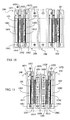
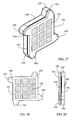
Fig. 4 is a perspective structural schematic view of the present invention showing that an insulator is installed between the side electrode plate being made with a current collecting terminal respectively at the two end-sides thereof and the flat plate type auxiliary electric conductor being respectively made with a current collecting terminal at the two end-sides thereof. -
Fig. 5 is a front view ofFig. 4 . -
Fig. 6 is a side view ofFig. 4 . -
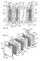
Fig. 7 is a decomposed schematic view of the embodiment showing that the side positive electrode plate (1011) is combined with the positive auxiliary electric conductor (1001), and the side negative electrode plate (1012) is combined with negative auxiliary electric conductor (1002) thereby constituting the electrode pair of the electricity storage/discharge device. -
Fig. 8 is an assembly schematic view of the embodiment showing the electrode pair to constitute the electricity storage/discharge device shown inFig. 7 . -
Fig. 9 is a schematic view showing the electricity storage/discharge device constituted by the electrode pair shown inFig. 8 being installed inside the casing (200) and the electric current flow path thereof. -
Fig. 10 shows the embodiment and the electric current flow path of multiple electricity storage/discharge devices as shown inFig. 9 being series connected outside the casing. -
Fig. 11 shows the embodiment and the electric current flow path of multiple electricity storage/discharge devices as shown inFig. 9 being series connected inside the casing. -
Fig. 12 shows the embodiment and the electric current flow path of the multiple electricity storage/discharge devices as shown inFig.11 being installed with the middle electrode cells constituted by the middle positive electrode plate (1013) and the middle negative electrode plate (1014) to be commonly series connected. -
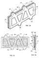
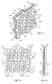
Fig. 13 is a decomposed schematic view showing that the side electrode plates being combined with auxiliary electric conductors appear multi-pairs of electrode plates in the stacked structure. -
Fig. 14 is an assembly schematic view showing that the side electrode plates being combined with auxiliary electric conductors appear multi-pairs of electrode plates in the stacked structure. -
Fig. 15 shows that the side electrode plates being combined with auxiliary electric conductors are stacked inside electrode cells, wherein the current collecting terminals of the same polarity of the multi-pairs of electrode plates are in parallel connection. -
Fig. 16 shows the electric current flow path of that side electrode plates being combined with auxiliary electric conductors are stacked inside multiple electrode cells, wherein the current collecting terminals of the multi-pairs of electrode plates in the same polarity are in parallel connection, while the input/output current terminals of individual electrode cells are series connected in forward polarities outside the casing. -
Fig. 17 shows the electric current path of that side electrode plates being combined with auxiliary electric conductors are stacked inside multiple electrode cells, wherein the current collecting terminals of the multi-pairs of electrode plates inside the multiple electrode cells are parallel connected, then the current collecting terminals of individual electrode cells are further series connected in forward polarities. -
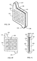
Fig. 18 is a perspective structural schematic view of the present invention showing that an insulator is interposed between the side electrode plate being made with a current collecting terminal respectively at the two end-sides thereof and the flat plate type auxiliary electric conductor with weight reducing concave holes being respectively made with a current collecting terminal at the two end-sides thereof. -
Fig. 19 is the front view ofFig. 18 . -
Fig. 20 is the side view ofFig. 18 . -
Fig. 21 is a perspective structural schematic view of the present invention showing that an insulator is interposed between the side electrode plate being made with two current collecting terminals respectively at the two end-sides thereof and the flat plate type auxiliary electric conductor being respectively made with two current collecting terminals at the two end-sides thereof. -
Fig. 22 is the front view ofFig. 21 . -
Fig 23 is the side view ofFig. 21 . -
Fig. 24 is a perspective structural schematic view of the present invention showing that an insulator is interposed between the side electrode plate being made with two current collecting terminals respectively at the two end-sides thereof and the flat plate type auxiliary electric conductor with weight reducing concave holes being respectively made with two current collecting terminals at the two end-sides thereof. -
Fig. 25 is the front view ofFig. 24 . -
Fig. 26 is the side view ofFig. 24 . -
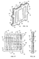
Fig. 27 is a perspective structural schematic view of the present invention showing that an insulator is interposed between the side electrode plate being made with a current collecting terminal respectively at the four end-sides thereof and the flat plate type auxiliary electric conductor being respectively made with a current collecting terminal at the four end-sides thereof. -
Fig. 28 is the front view ofFig. 27 . -
Fig. 29 is the side view ofFig. 27 . -
Fig. 30 is a perspective structural schematic view of the present invention showing that an insulator is interposed between the side electrode plate being made with a current collecting terminal respectively at the four end-sides thereof and the flat plate type auxiliary electric conductor with weight reducing concave holes being respectively made with a current collecting terminals at the four end-sides thereof. -
Fig. 31 is the front view ofFig. 30 . -
Fig. 32 is the side view ofFig. 30 . -
Fig. 33 is a perspective structural schematic view of the present invention showing that an insulator is interposed between the side electrode plate being made with two current collecting terminals respectively at the four end-sides thereof and the flat plate type auxiliary electric conductor being respectively made with two current collecting terminals at the four end-sides thereof. -
Fig. 34 is the front view ofFig. 33 . -
Fig. 35 is the side view ofFig. 33 . -
Fig. 36 is a perspective structural schematic view of the present invention showing that an insulator is interposed between the side electrode plate being made with two current collecting terminals respectively at the four end-sides thereof and the flat plate type auxiliary electric conductor with weight reducing concave holes being respectively made with two current collecting terminals at the four end-sides thereof. -
Fig. 37 is the front view ofFig. 36 . -
Fig. 38 is the side view ofFig. 36 . -
Fig. 39 is a structural schematic view of the embodiment showing that the neighborhood near to the input/output current collecting terminal at the electrode plate of the present invention is outwardly slantingly widened thereby forming the electrode plate structure comprising mesh type conductor having gradually increased effective current transmission area. -
Fig. 40 is the front view ofFig. 39 . -
Fig. 41 is the side view ofFig. 39 . -
Fig. 42 is a structural schematic view of the embodiment showing that the space of the electrode plate of the present invention for installing active matter (120) used for generating electricity storage/discharge function is in a lattice shape and slants to the frame of the mesh-lattice type current collecting conductor at outer side of the electrode plate, so as to allow the neighborhood near to the input/output current collecting terminal to be outwardly slantingly widened thereby forming the mesh type conductor having gradually increased effective current transmission area at locations nearer to the input/output current collecting terminals. -
Fig. 43 is the front view ofFig. 42 . -
Fig. 44 is the side view ofFig.42 . -
- P100: Electrode plate
- T100: Current collecting terminal
- 100: Auxiliary electric conductor
- 101: Side electrode plate
- 103: Insulator
- 104, 106, 1041, 1042, 1061, 1062, 1081, 1091: current collecting terminal
- 105, 107, 1051, 1052, 1071, 1072: Input/output current collecting terminal
- 108: weight reducing concave hole
- 120: Active matter
- 200: Casing
- 1001: Positive auxiliary electric conductor
- 1002: Negative auxiliary electric conductor
- 1011: Side positive electrode plate
- 1012: Side negative electrode plate
- 1013: Middle positive electrode plate
- 1014: Middle negative electrode plate
- 1020: Isolating plate
- The present invention discloses an improved multi-end sides to single end side input/output current collecting terminal structure being applied to the electrode plate of an electricity storage/discharge device for applications in electricity storage/discharge devices such as primary batteries, secondary chargeable/dischargeable batteries, capacitors, or super-capacitors, or fuel cell power supply device having electrode plates, wherein two or more than two end sides of each electrode plate of above said device are made with one or more than one current collecting terminal structure thereby allowing the electrode plate via multiple current collecting terminals on multi-sides to collect currents in multi-circuits, wherein the auxiliary electric conductor is additionally installed between the positive or negative electrode plate installed on end-side of individual electrode cell and the electrode cell casing, and the insulator is installed between the electrode plate and the auxiliary electric conductor thereby allowing current collecting terminals at different end-sides of the electrode plates in the same polarity to be connected via the auxiliary electric conductors to collect the currents of current collecting terminals at multiple end sides to the current collecting terminal at single end side to facilitate collecting input/output currents to the outside, wherein the number of external input/output current collecting terminals on the single end side of electrode plate can be one more than one.
- The main constitution characteristics of the electrode plate multi-end sides to single end side current collector of an electricity storage/discharge device of the present invention are as following:
- -- The individual electrode cell is provided for disposing a stack of electrode plates, wherein at where between the positive or negative electrode plate installed near the end-side of the electrode cell and the electrode cell casing is additionally installed with the auxiliary electric conductor, and the insulator is further interposed between said electrode plate and said auxiliary electric conductor, thereby the current collecting terminals at different end sides of the electrode plate in the same polarity are connected via the auxiliary electric conductor to collect currents from current collecting terminals at multiple end sides to the current collecting terminal at single end side for the current collecting terminal at single end side being used as the external input/output current collecting terminal, wherein the number of the external input/output current collecting terminal installed on the single end side can be one more than one;
- -- The auxiliary electric conductor being in flat plate or bar shape, or multi-barred shape, or of flat plate type structure with concave holes (including through holes or blind holes), or of mesh type structure, or in other selected geometric shape and being made of selected electrically conductive material are used to connect current collecting terminals at different end sides of the side electrode plate thereby allowing currents of current collecting terminals at multiple end sides to be collected to the current collecting terminal at single end side for the current collecting terminal at single end side being used as the external input/output current collecting terminal, wherein the number of the external input/output current collecting terminals installed on the single end side can be one more than one;
- -- The auxiliary electric conductor is installed between the end-side of the internal electrode cell and the side electrode plate and an insulator is further interposed between said auxiliary electric conductor and its attached side electrode plate; the auxiliary electric conductor and its attached side electrode plate are respectively disposed with output current collecting terminals at the at least end sides, wherein the combination methods between the output current collecting terminals of the two include welding, fusion joining, rivet fastening, lockingly combined by screw, or pressingly combined by prestress, internally buried, or embedment or other methods, or the auxiliary electric conductor and the side electrode plate are integrally made, or the auxiliary electric conductor and the side electrode plate are connectedly made to foil type and are further folded to combine the input/output current collecting terminals at the other end by above said welding, fusion joining, rivet fastening, lockingly combined by screw, or pressingly combined by prestress, internally buried, or embedment or other methods so as to electrically connect respective current collecting terminals at different end sides of the side electrode plate in the same electrode cell thereby allowing the currents of current collecting terminals at multiple end sides being collected to the current collecting terminal at single end side being connected and combined by the side electrode plate and the auxiliary electric conductor for the current collecting terminal at single end side being used as the external input/output current collecting terminal, wherein the number of external input/output current collecting terminal installed on the single end side of the side electrode plate and the auxiliary electric conductor can be one more than one;
- -- The conductors for series connecting the input/output current collecting terminals of the electrode plates in different polarities in different electrode cells are further made of connected foil or bar type conductors by selected geometric shape and selected material;
- The installation methods of the insulators interposed between the side electrode plate of the end-side of the electrode cell and the auxiliary electric conductor can be constituted by one or more than one method as following, include:
- 1) Both of the electrode cell casing as well as the insulator being interposed between the side electrode plate (101) and the auxiliary electric conductor (100) can be made of different insulation materials;
- 2) Both of the electrode cell casing as well as the insulator being interposed between the side electrode plate (101) and the auxiliary electric conductor (100) can be constituted by individual structures made of the same insulation materials;
- 3) The electrode cell casing as well as the insulator being interposed between the side electrode plate (101) and the auxiliary electric conductor (100) can be integrally constituted by the same insulation material;
- 4) The insulator interposed between the side electrode plate (101) and the auxiliary electric conductor (100) is constituted by the originally enclosed or further treated insulation layer on the surface of the electrode plate or the auxiliary electric conductor itself.
- The electrode plate multi-end sides to single end side current collector of an electricity storage/discharge device of the present invention is further made by connecting electric conductors to connect the current collecting terminals of the individual electrode plates in the same voltage and the same polarity installed inside the same or different electrode cells for parallel connection, or to connect the current collecting terminals of electrode plates in opposite polarities installed inside different electrode cells for series connection or mixed series and parallel connection;
- Aforesaid design concept can be applied in numerous adopted structural methods for practical requirements, wherein the structural types of flat plate type auxiliary electric conductors having said structural features are described in the following:
-
Fig. 4 is a perspective structural schematic view of the present invention showing that an insulator is installed between the side electrode plate being made with a current collecting terminal respectively at the two end-sides thereof and the flat plate type auxiliary electric conductor being respectively made with a current collecting terminal at the two end-sides thereof. -
Fig. 5 is a front view ofFig. 4, and Fig. 6 is a side view ofFig. 4 . - For the structure shown in aforesaid
Fig. 4, Fig. 5 and Fig. 6 , the constitution characteristics include: - -- The side electrode plate (101) is respectively made with a current collecting terminal at the two end-sides thereof;
- -- An insulator (103) is installed between one side of the side electrode plate (101) and the additionally outside installed flat plate type auxiliary electric conductor (100), while the other side of the side electrode plate (101) has a lattice type space to install conventional active matter (102) used for generating electricity storage/discharge function;
- -- The current collecting terminal (104) of the side electrode plate (101) and the current collecting terminal (106) of the auxiliary electric conductor (100) on the same end are parallel connected for electric conduction;
- -- The input/output current collecting terminal (105) of the side electrode plate (101) is parallel connected with the current collecting terminal (107) of the auxiliary electric conductor (100) on the same end for electric conduction to constitute input/output current collecting function for common input or output currents.
- The insulator (103) is interposed between aforesaid side electrode plate (101) and auxiliary electric conductor (100) which are parallel connected via current collecting terminals (104, 106) for electric conduction and are through the parallel connection between the input/output current collecting terminals (105, 106) for electric conduction thereby constituting the input/output current collecting function for common input or output currents to the outside.
- Further, said current collecting terminals (104, 106) on the other end thereof not arranged for common input/output currents to the outside can also be not made in terminal structures but to directly parallel connect the side electrode plate (101) and the auxiliary electric conductor (100) at the positions equivalent to the positions of electric conducting structures of the current collecting terminal (104) and the current collecting terminal (106) for electric conduction.
- The aforesaid side electrode plate (101) as shown in
Fig. 4 further can respectively be used as the side positive electrode plate (1011) and the side negative electrode plate (1012) constituting the electricity storage/discharge device to form a positive and negative electrode pair, wherein: - The insulator (103) is interposed between the side positive electrode plate (1011) and the positive auxiliary electric conductor (1001), while the current collecting terminal (1041) of the side positive electrode plate (1011) and the current collecting terminal (1061) of the positive auxiliary electric conductor (1001) are parallel connected for electric conduction, as well as the input/output current collecting terminal (1051) of the side positive electrode plate (1011) and the input/output current collecting terminal (1071) of the positive auxiliary electric conductor (1001) are parallel connected for electric conduction thereby providing the input/output current function to the outside;
- The insulator (103) is interposed between the side negative electrode plate (1012) and the negative auxiliary electric conductor (1002), while the current collecting terminal (1042) of the side negative electrode plate (1012) and the current collecting terminal (1062) of the negative auxiliary electric conductor (1002) are parallel connected for electric conduction, as well as the input/output current collecting terminal (1052) of the side negative electrode plate (1012) and the input/output current collecting terminal (1072) of the negative auxiliary electric conductor (1002) are parallel connected for electric conduction thereby providing the input/output current function to the outside;
- The separator plate (1020) is interposed between aforesaid side positive electrode plate (1011) and side negative electrode plate (1012);
- The joined surfaces of aforesaid side positive electrode plate (1011) and side negative electrode plate (1012) for joining the separator plate (1020) has a lattice type space to install conventional active matter (102) used for generating electricity storage/discharge function;
-
Fig. 7 is a decomposed schematic view of the embodiment showing that the side positive electrode plate (1011) is combined with the positive auxiliary electric conductor (1001), and the side negative electrode plate (1012) is combined with the negative auxiliary electric conductor (1002) thereby constituting the electrode pair of the electricity storage/discharge device; -
Fig. 8 is an assembly schematic view of the embodiment showing the electrode pair to constitute the electricity storage/discharge device shown inFig. 7 ; -
Fig. 9 is a schematic view showing the electricity storage/discharge device constituted by the electrode pair shown inFig. 8 being installed inside the casing (200) and the electric current flow path thereof. - As shown in
Fig. 9 , the casing (200) is used for constituting the casing of the electricity storage/discharge device and is made of insulation material, wherein it can be optionally made to required structural shapes as needed. -
Fig. 10 shows the embodiment and the electric current flow path of multiple electricity storage/discharge devices as shown inFig. 9 being series connected outside the casing; - As shown in
Fig. 10 , the electrode cell with two or more than two individual casings (200) is arranged for individually housing a stack of electrode plates including housing the side positive electrode plate (1011) and the side negative electrode plate (1012), wherein:- The insulator (103) is interposed between the side positive electrode plate (1011) and the positive auxiliary electric conductor (1001) as well as interposed between the side negative electrode plate (1012) and the negative auxiliary electric conductor (1002); the external input/output positive current collecting terminals and the external input/output negative current collecting terminals in the individual electrode cells are series connected in forward polarities for input/output currents to the outside.
-
Fig. 11 shows the embodiment and the electric current flow path of multiple electricity storage/discharge devices as shown inFig. 9 being series connected inside the casing; - As shown in
Fig. 11 , it is constituted of that:- In the electrode cell with an integrated casing (200) for housing the positive input/output current collecting terminals, the insulator (103) is interposed between the side positive electrode plate (1011) and the positive auxiliary electric conductor (1001), wherein the positive input/output current collecting terminals (1071, 1051) of the two are connected for electric conduction in common to provide input/output currents to the outside;
- Regarding the electrode cell with an integrated casing (200) for housing the negative input/output current collecting terminals, the insulator (103) is interposed between the side negative electrode plate (1012) and the negative auxiliary electric conductor (1002), wherein the negative input/output current collecting terminals (1072, 1052) of the two are connected for electric conduction to provide input/output currents to the outside.
- Said side positive electrode plate (1011) and side negative electrode plate (1012) are respectively installed at the end side of the individual electrode cells inside an integrated casing (200), and the side positive electrode plate (1011) is attached to the separately installed middle negative electrode plate (1014) via a separator plate (1020) in the same electrode cell, while the side negative electrode plate (1012) is attached to the middle positive electrode plate (1013) via a separator plate (1020) in another electrode cell, thereby the current collecting terminals (1081) at two end-sides of the middle positive electrode plate (1013) in one electrode cell and the current collecting terminals (1091) at the two end-sides of the middle negative electrode plate (1014) in another electrode cell are series connected for electric conduction.
-
Fig. 12 shows the embodiment and the electric current flow path of the multiple electricity storage/discharge devices as shown inFig.11 being installed with the middle electrode cells constituted by the middle positive electrode plate (1013) and the middle negative electrode plate (1014) to be commonly series connected; - As shown in
Fig. 12 , individual middle electrode cells are further series connected between the electrode cell having the side positive electrode plate (1011) and the middle negative electrode plate (1014), and the electrode cell having the side negative electrode plate (1012) and the middle positive electrode plate (1013), wherein the middle electrode cell is installed with the middle positive electrode plate (1013) and the middle negative electrode plate (1014), while the current collecting terminals (1081) at the two end-sides of the middle positive electrode plate (1013), and the current collecting terminals (1091) at the two end-sides of the middle negative electrode plate (1014) in the same middle electrode cell are respectively series connected with the current collecting terminals (1081) at the two end-sides of the middle positive electrode plate (1013) and the current collecting terminals (1091) at the two end-sides of the middle negative electrode plate (1014) in different polarities in neighboring electrode cell for electric conduction, wherein the insulators (103) are respectively interposed between the side positive electrode plate (1011) and the positive auxiliary electric conductor (1001), and between the side negative electrode plate (1012) and the negative auxiliary electric conductor (1002), while the external positive input/output current collecting terminals and the external negative input/output current collecting terminals in the individual electrode cells provide input/output current to the outside.- For the electrode plate multi-end sides to single end side current collector of an electricity storage/discharge device of present invention, the electrode plates in the same polarity within the same electrode cell inside the casing (200) are further parallel connected;
-
Fig. 13 is a decomposed schematic view showing that the side electrode plates being combined with auxiliary electric conductors appear multi-pairs of electrode plates in the stacked structure. -
Fig. 14 is an assembly schematic view showing that the side electrode plates being combined with auxiliary electric conductors appear multi-pairs of electrode plates in the stacked structure. -
Fig. 15 shows that the side electrode plates being combined with auxiliary electric conductors are stacked inside electrode cells, wherein the current collecting terminals of the same polarity of the multi-pairs of electrode plates are in parallel connection. - In the embodiments shown in
Figs. 13 ,14 and 15 , the side electrode plate (101) of the stack of electrode plates as shown inFig. 4 are respectively made to the side positive electrode plate (1011) and the side negative electrode plate (1012), wherein the insulator (103) is interposed between the side positive electrode plate (1011) and the positive auxiliary electric conductor (1001), while the current collecting terminal (1041) of the side positive electrode plate (1011) and the current collecting terminal (1061) of the positive auxiliary electric conductor (1001) are parallel connected for electric conduction, as well as the input/output current collecting terminal (1051) of the side positive electrode plate (1011) and the input/output current collecting terminal (1071) of the positive auxiliary electric conductor (1001) are parallel connected for input/output currents to the outside; - The insulator (103) is interposed between the side negative electrode plate (1012) and the negative auxiliary electric conductor (1002), while the current collecting terminal (1042) of the side negative electrode plate (1012) and the current collecting terminal (1062) of the negative auxiliary electric conductor (1002) are parallel connected for electric conduction, as well as the input/output current collecting terminal (1052) of the side negative electrode plate (1012) and the input/output current collecting terminal (1072) of the negative auxiliary electric conductor (1002) are parallel connected for input/output currents to the outside;
- The separator plates (1020) are respectively interposed between the side positive electrode plate (1011) and the neighboring middle negative electrode plate (1014), and between the middle negative electrode plate (1014) and the neighboring middle positive electrode plate (1013), as well as between the middle positive electrode plate (1013) and the neighboring side negative electrode plate (1012);
- The current collecting terminals of aforesaid side positive electrode plate (1011) and aforesaid middle positive electrode plate (1013) on the same ends are parallel connected for electric conduction, and the current collecting terminals of the side negative electrode plate (1012) and the middle negative electrode plate (1014) are also parallel connected for electric conduction,
wherein the number of middle positive electrode plates (1013) and middle negative electrode plates (1014) is one or more than one thereby constituting the structure of multiple pairs of electrode plates in parallel connection for electric conduction.
- The joined surfaces of aforesaid side positive electrode plate (1011), side negative electrode plate (1012), middle positive electrode plate (1013), middle negative electrode plate (1014) for joining the separator plate (1020) has a lattice type space to install conventional active matter (102) used for generating electricity storage/discharge function.
- The embodiments shown in
Figs. 13 ,14, 15 are further constituted by that multiple independent or integrated electrode cells having multiple parallel connected electrode plates of the same polarity are series connected via the input/output terminals in different polarities for voltage selection. -
Fig. 16 shows the electric current flow path of that side electrode plates being combined with auxiliary electric conductors are stacked inside multiple electrode cells, wherein the current collecting terminals of the multi-pairs of electrode plates in the same polarity are in parallel connection, while the input/output current terminals of individual electrode cells are series connected in forward polarities outside the casing; - As shown in
Fig. 16 , it is constituted of that:- The electrode cells with individual casings (200) are arranged for individually housing a stack of electrode plates including housing the side positive electrode plate (1011) and the side negative electrode plate (1012), wherein:
- The insulator (103) is interposed between the side positive electrode plate (1011) and the positive auxiliary electric conductor (1001) which are parallel connected via the positive input/output current collecting terminals (1071, 1051) thereof for electric conduction to provide input/output currents to the outside, and are parallel connected with the current collecting terminal (1081) of the middle positive electrode plate (1013) in the same electrode cell, while the current collecting terminals (1041, 1061) at the other side of the same electrode plate are parallel connected with the current collecting terminals (1081) of the middle positive electrode plate (1013) in the same electrode cell;
- The insulator (103) is interposed between the side negative electrode plate (1012) and the negative auxiliary electric conductor (1002) which are parallel connected via the negative input/output current collecting terminals (1052, 1072) for electric conduction to provide input/output currents to the outside, and are parallel connected with the current collecting terminal (1091) of the middle negative electrode plate (1014) in the same electrode cell, while the current collecting terminals (1042, 1062) at the other side of the same side negative electrode plate (1012) are parallel connected with the current collecting terminals (1091) of the middle negative electrode plate (1014) in the same electrode cell, wherein the individual input/output current collecting terminals are externally exposed outside the casing (200) for series or parallel connection to provide input/output currents to the outside.
- The electrode cells with individual casings (200) are arranged for individually housing a stack of electrode plates including housing the side positive electrode plate (1011) and the side negative electrode plate (1012), wherein:
-
Fig. 17 shows the electric current path of that side electrode plates being combined with auxiliary electric conductors are stacked inside multiple electrode cells, wherein the current collecting terminals of the multi-pairs of electrode plates inside the multiple electrode cells are parallel connected, then the current collecting terminals of individual electrode cells are further series connected in forward polarities; - As shown in
Fig. 17 , it is constituted of that:- In the electrode cells in the integrated casing (200) for housing positive electrode input/output current collecting terminals, an insulator (103) is interposed between the side positive electrode plate (1011) and the positive auxiliary electric conductor (1001), which are parallel connected via the positive input/output current collecting terminals (1071, 1051) for providing input/output currents to the outside, and are parallel connected with the middle positive electrode plate (1013) in the electrode cell;
- In the electrode cell of integrated casing (200) for housing negative electrode input/output current collecting terminals, an insulator (103) is interposed between the side negative positive electrode plate (1012) and the negative auxiliary electric conductor (1002) which are parallel connected via the negative electrode input/output current collecting terminals (1072, 1052) for providing input/output currents to the outside, and are parallel connected with the middle negative electrode plate (1014) in the electrode cell;
- As shown in aforesaid
Fig. 17 , it is constructed by that the side positive electrode plate (1011) and the side negative electrode plate (1012) are respectively installed on the end sides of their individually belonging electrode cells of the integrated casing (200), while besides the side positive electrode plate (1011) and the middle negative electrode plate (1014), at least one middle positive electrode plate (1013) and one middle negative electrode plate (1014) in positive-negative polarity order shall be installed in the electrode cell, as well as the side negative electrode plate (1012) and the middle positive electrode plate (1013) are installed in another electrode cell, and at least one middle positive electrode plate (1013) and one middle negative electrode plate (1014) in positive-negative polarity order shall be installed in another electrode cell, wherein the current collecting terminals (1041, 1051) at the two end-sides of the side positive electrode plate (1011), the current collecting terminals (1061, 1071) at the two end-sides of the positive auxiliary electric conductor (1001), and the current collecting terminals (1081) at the two end-sides of the middle positive electrode plate (1013) of the same polarity in the same electrode cell are parallel connected, and the current collecting terminals (1042, 1052) at the two sides of the side negative electrode plate (1012), the current collecting terminals (1062, 1072) at the two end-sides of the negative auxiliary electric conductor (1002), and the current collecting terminals (1091) at the two end-sides of the middle negative electrode plate (1014) of the same polarity in another electrode cell are parallel connected; wherein respective current collecting terminals at the two end-sides of the middle positive electrode plate (1013) and at the two end-sides of the middle negative electrode plate (1014) of neighboring electrode cells in different polarities are series connected for electric conduction.
- The auxiliary electric conductor (100) including the positive auxiliary electric conductor (1001) and the negative auxiliary electric conductor (1002) of the electrode plate multi-end sides to single end side current collector of an electricity storage/discharge device of the present invention are optionally selectively made to following one or more than one geometric shapes of electrode plate structure on the condition for favorable current transmission; including:
- 1) As shown in
Fig. 18 is a perspective structural schematic view of the present invention showing that an insulator is interposed between the side electrode plate being made with a current collecting terminal respectively at the two end-sides thereof and the flat plate type auxiliary electric conductor with weight reducing concave holes being respectively made with a current collecting terminal at the two end-sides thereof;-
Fig. 19 is the front view ofFig. 18 ; -
Fig. 20 is the side view ofFig. 18 .
Fig 18, Fig. 19 and Fig. 20 , it is constructed by that the insulator (103) is interposed between the side electrode plate (101) being made with an external input/output current collecting terminal (105) at one end side thereof and a current collecting terminal (104) at the other end side thereof; and the flat plate type auxiliary electric conductor (100) with weight reducing concave holes (108) being made with an external input/output current collecting terminal (107) thereof and a current collecting terminal (106) at the other end side thereof,
wherein the external input/output current collecting terminals (105, 107) and the current collecting terminals (104, 106) on the same sides of the side electrode plate (101) and the auxiliary electric conductor (100) are respectively parallel connected for electric conduction. -
- 2) As shown in
Fig. 21 is a perspective structural schematic view of the present invention showing that an insulator is interposed between the side electrode plate being made with two current collecting terminals respectively at the two end-sides thereof and the flat plate type auxiliary electric conductor being respectively made with two current collecting terminals at the two end-sides thereof;-
Fig. 22 is the front view ofFig. 21 ; -
Fig 23 is the side view ofFig. 21 .
Fig. 21, Fig. 22 and Fig. 23 , it is constructed by that the insulator (103) is interposed between the side electrode plate (101) being made with two external input/output current collecting terminals (105) and two current collecting terminals (104) respectively at the two end-sides thereof, and the flat plate type auxiliary electric conductor (100) being made with two external input/output current collecting terminals (107) and two current collecting terminals (106) respectively at the two end-sides thereof, wherein the current collecting terminals on the same sides of the side electrode plate (101) and the auxiliary electric conductor (100) are parallel connected thereby allowing the two connected current collecting terminals for input/output currents on the same end side either being further parallel connected for electric conduction to provide input/output currents to the outside, or not being parallel connected but provide input/output currents to the outside individually. -
- 3) As shown in
Fig. 24 is a perspective structural schematic view of the present invention showing that an insulator is interposed between the side electrode plate being made with two current collecting terminals respectively at the two end-sides thereof and the flat plate type auxiliary electric conductor with weight reducing concave holes being respectively made with two current collecting terminals at the two end-sides thereof;-
Fig. 25 is the front view ofFig. 24 ; -
Fig. 26 is the side view ofFig. 24 .
Fig. 24, Fig. 25 and Fig. 26 , it is constructed by that the insulator (103) is interposed between the side electrode plate (101) being made with two external input/output current collecting terminals (105) and two current collecting terminals (104) respectively at the two end-sides thereof, and the flat plate type auxiliary electric conductor (100) with weight reducing concave holes (108) being made with two external input/output current collecting terminals (107) and two current collecting terminals (106) respectively at the two end-sides thereof, wherein the current collecting terminals on the same sides of the side electrode plate (101) and the auxiliary electric conductor (100) are parallel connected thereby allowing the connected current collecting terminals for input/output currents on the same end side either being further parallel connected for electric conduction to provide input/output currents to the outside, or not being parallel connected but provide input/output currents to the outside individually. -
- 4) As shown in
Fig. 27 is a perspective structural schematic view of the present invention showing that an insulator is interposed between the side electrode plate being made with a current collecting terminal respectively at the four end-sides thereof and the flat plate type auxiliary electric conductor being respectively made with a current collecting terminal at the four end-sides thereof;-
Fig. 28 is the front view ofFig. 27 . -
Fig. 29 is the side view ofFig. 27 .
Fig. 27, Fig. 28 and Fig. 29 , it is constructed by that the insulator (103) is interposed between the side electrode plate (101) being made with a current collecting terminal respectively at the four end-sides thereof, and the flat plate type auxiliary electric conductor (100) being respectively made with a current collecting terminal at the four end-sides thereof, wherein the current collecting terminals on the same sides of the side electrode plate (101) and the auxiliary electric conductor (100) are respectively parallel connected thereby allowing the connected current collecting terminals for input/output current at the respective same end sides being further parallel connected for electric conduction to provide input/output currents to the outside. -
- 5) As shown in
Fig. 30 is a perspective structural schematic view of the present invention showing that an insulator is interposed between the side electrode plate being made with a current collecting terminal respectively at the four end-sides thereof and the flat plate type auxiliary electric conductor with weight reducing concave holes being respectively made with a current collecting terminals at the four end-sides thereof;-
Fig. 31 is the front view ofFig. 30 ; -
Fig. 32 is the side view ofFig. 30 .
Fig. 30, Fig. 31 and Fig. 32 , it is constructed by that the insulator (103) is interposed between the side electrode plate (101) being made with a current collecting terminal respectively at the four end-sides thereof, and the flat plate type auxiliary electric conductor (100) with weight reducing concave holes (108) being respectively made with a current collecting terminals at the four end-sides thereof, wherein the current collecting terminals one the same sides of the side electrode plate (101) and the auxiliary electric conductor (100) are respectively parallel connected thereby allowing the connected current collecting terminals for input/output current at the respective same end sides being further parallel connected for electric conduction to provide input/output currents to the outside. -
- 6) As shown in
Fig. 33 is a perspective structural schematic view of the present invention showing that an insulator is interposed between the side electrode plate being made with two current collecting terminals respectively at the four end-sides thereof and the flat plate type auxiliary electric conductor being respectively made with two current collecting terminals at the four end-sides thereof;-
Fig. 34 is the front view ofFig. 33 ; -
Fig. 35 is the side view ofFig. 33 .
Fig. 33, Fig. 34 and Fig. 35 , it is constructed by that the insulator (103) is interposed between the side electrode plate (101) being made with two current collecting terminals respectively at the four end-sides thereof, and the flat plate type auxiliary electric conductor (100) being respectively made with two current collecting terminals at the four end-sides thereof, wherein the current collecting terminals on the same sides of the side electrode plate (101) and the auxiliary electric conductor (100) are respectively parallel connected thereby allowing the connected current collecting terminals for input/output current at the respective same end sides being either further parallel connected for electric conduction to provide input/output current to the outside, or individually used to provide input/output currents to the outside. -
- 7) As shown in
Fig. 36 is a perspective structural schematic view of the present invention showing that an insulator is interposed between the side electrode plate being made with two current collecting terminals respectively at the four end-sides thereof and the flat plate type auxiliary electric conductor with weight reducing concave holes being respectively made with two current collecting terminals at the four end-sides thereof;-
Fig. 37 is the front view ofFig. 36 ; -
Fig. 38 is the side view ofFig. 36 .
-
- As shown in aforesaid
Fig. 36, Fig. 37 and Fig. 38 , it is constructed by that the insulator (103) is interposed between the side electrode plate (101) being made with two current collecting terminals respectively at the four end-sides thereof, and the flat plate type auxiliary electric conductor (100) with weight reducing concave holes (108) being respectively made with two current collecting terminal at the four end-sides thereof, wherein the current collecting terminals on the same sides of the side electrode plate (101) and the auxiliary electric conductor (100) are respectively parallel connected thereby allowing the connected current collecting terminals for input/output current at the respective same end sides being either further parallel connected for electric conduction to provide input/output current to the outside, or individually used to provide input/output currents to the outside. - The above described embodiments 1)∼7) are simply structural application examples which are not used for limitations, i.e. the auxiliary electric conductor (100) including the positive auxiliary electric conductor (1001) and the negative auxiliary electric conductor (1002) of the electrode plate multi-end sides to single end side current collector of an electricity storage/discharge device of the present invention is optionally selectively made to one or more than one geometric shapes as needed on the condition of favorable current transmission.
- Besides, for enhancing the electrode plate current collecting function of the current collecting terminals (T100) installed on all or partial electrode plates, including for enhancing the electrode plate current collecting function of the current collecting terminals (T100) installed on the side electrode plate (101), the side positive electrode plate (1011), the side negative electrode plate (1012), the middle positive electrode plate (1013), or the middle negative electrode plate (1014), the lattice shape space for installing active matter (120) with electricity storage/discharge function on aforesaid all or partial electrode plates and the electric conducting structure at outside frame of electrode plates have larger effective electric conducting area at the location nearer to the input/output current collecting terminal (T100), thereby reducing the impedance and favoring the uniformed transmission of current density;
-
Fig. 39 is a structural schematic view of the embodiment showing that the neighborhood near to the input/output current collecting terminal at the electrode plate of the present invention is outwardly slantingly widened thereby forming the electrode plate structure comprising current collecting conductor having gradually increased effective current transmission area; -
Fig. 40 is the front view ofFig. 39 ; -
Fig. 41 is the side view ofFig. 39 ; - As shown in aforesaid
Fig.39, Fig.40 and Fig.41 , for enhancing the electrode plate current collecting function of the current collecting terminals (T100) installed on all or partial electrode plates, including for enhancing the electrode plate current collecting function of the current collecting terminals (T100) installed on the side electrode plate (101), the side positive electrode plate (1011), the side negative electrode plate (1012), the middle positive electrode plate (1013), or the middle negative electrode plate (1014), the electric conducting structure at outside frame of said all or partial electrode plates at neighborhood nearer to the input/output current collecting terminals (T100) have larger effective electric conducting cross-sectional area, wherein the structural characteristic includes outwardly slantingly gradually widened, or gradually thicker, or both gradually widen and thicker, thereby forming the structure of current collecting conductor to have more gradually increased effective current transmission area at locations nearer to the input/output current terminals; - Based on the same rationale, said structure for enhancing the electrode plate current collecting function of current collecting terminals further includes the electrode plates being applied in conventional electricity storage device comprising electricity storage/discharge device of conventional primary battery, secondary chargeable/dischargeable battery, capacitors, or super-capacitors, or fuel cell power supply device having electrode plates;
- Further,
Fig. 42 is a structural schematic view of the embodiment showing that at where between the lattice shape space of the electrode plate of the present invention for installing the active matter (120) with electricity storage/discharge function and the outside mesh type current collecting conductor at outside frame of electrode plate appears a slanted mesh-lattice shape structure, so as to allow the neighborhood near to the input/output current collecting terminal to be outwardly slantingly widened thereby forming the mesh type conductor having gradually increased effective current transmission area at locations nearer to the input/output current collecting terminals; -
Fig. 43 is the front view ofFig. 42 ; -
Fig. 44 is the side view ofFig.42 ; - As shown in aforesaid
Fig. 42, Fig. 43 and Fig. 44 , for enhancing the electrode plate current collecting function of the current collecting terminals (T100) installed on all or partial electrode plates, including for enhancing the electrode plate current collecting function of the current collecting terminals (T100) installed on the side electrode plate (101), the side positive electrode plate (1011), the side negative electrode plate (1012), the middle positive electrode plate (1013), or the middle negative electrode plate (1014), at where between the lattice shape space of aforesaid all or partial electrode plates for installing active matter (120) used for generating electricity storage/discharge function and the mesh shape current collecting electric conductor of the electrode plate appears in a slanted mesh-lattice shape structure, so as to allow the neighborhood nearer to the input/output current collecting terminal of the electric conducting structure at outside frame of the electrode plate to be outwardly slantingly gradually widened, or gradually thicker, or both gradually widen and thicker, so that to increase effective current transmission area thereby forming the mesh type current collecting conducting structure to have more gradually increased effective current transmission area at neighborhood nearer to the input/output current terminals, and thereby forming the non-parallel slanted multi-lattice type structural relationship between the lattice type space of active matter (120) used for generating electricity storage/discharge function and the frame of outer side mesh type electric conductor. - Based on the same rationale, said structure for enhancing the electrode plate current collecting function of current collecting terminals further includes the electrode plates being applied in conventional electricity storage device comprising electricity storage/discharge device of conventional primary battery, secondary chargeable/dischargeable battery, capacitors, or super-capacitors, or fuel cell power supply device having electrode plates.
- According to the invention, an electricity storage/discharge device comprises an electrode plate (101) having a first current collecting terminal (104) and a first input/output current collecting terminal (105);
- an auxiliary conductor (100) having a second current collecting terminal (106) and a second input/output current collecting terminal (107); and
- an insulator (103) positioned between the side plate (101) and the auxiliary conductor (100);
wherein the first current collecting terminal (104) is electrically connected to the second current collecting terminal (106); and
wherein the first input/output current collecting terminal (105) is electrically connected to the second input/output current collecting terminal (107).
Claims (20)
- An electrode plate multi-end sides to single end side current collector of an electricity storage/discharge device is an improved multi-end sides to single end side input/output current collecting terminal structure being applied to the electrode plate of an electricity storage/discharge device for applications in electricity storage/discharge devices such as primary batteries, secondary chargeable/dischargeable batteries, capacitors, or super-capacitors, or fuel cell power supply device having electrode plates, wherein two or more than two end sides of each electrode plate of above said device are made with one or more than one current collecting terminal structure thereby allowing the electrode plate via multiple current collecting terminals on multi-sides to collect currents in multi-circuits,
wherein the auxiliary electric conductor is additionally installed between the positive or negative electrode plate installed on end-side of individual electrode cell and the electrode cell casing, and the insulator is installed between the electrode plate and the auxiliary electric conductor thereby allowing current collecting terminals at different end-sides of the electrode plates in the same polarity to be connected via the auxiliary electric conductors to collect the currents of current collecting terminals at multiple end sides to the current collecting terminal at single end side to facilitate collecting input/output currents to the outside, wherein the number of external input/output current collecting terminals on the single end side of electrode plate can be one more than one. - An electrode plate multi-end sides to single end side current collector of an electricity storage/discharge device as claimed in claim 1, wherein it mainly constituted as follows:-- The individual electrode cell is provided for disposing a stack of electrode plates, wherein at where between the positive or negative electrode plate installed near the end-side of the electrode cell and the electrode cell casing is additionally installed with the auxiliary electric conductor, and the insulator is further interposed between said electrode plate and said auxiliary electric conductor, thereby the current collecting terminals at different end sides of the electrode plate in the same polarity are connected via the auxiliary electric conductor to collect currents from current collecting terminals at multiple end sides to the current collecting terminal at single end side for the current collecting terminal at single end side being used as the external input/output current collecting terminal, wherein the number of the external input/output current collecting terminal installed on the single end side can be one more than one;-- The auxiliary electric conductor being in flat plate or bar shape, or multi-barred shape, or of flat plate type structure with concave holes (including through holes or blind holes), or of mesh type structure, or in other selected geometric shape and being made of selected electrically conductive material are used to connect current collecting terminals at different end sides of the side electrode plate thereby allowing currents of current collecting terminals at multiple end sides to be collected to the current collecting terminal at single end side for the current collecting terminal at single end side being used as the external input/output current collecting terminal, wherein the number of the external input/output current collecting terminals installed on the single end side can be one more than one;-- The auxiliary electric conductor is installed between the end-side of the internal electrode cell and the side electrode plate and an insulator is further interposed between said auxiliary electric conductor and its attached side electrode plate; the auxiliary electric conductor and its attached side electrode plate are respectively disposed with output current collecting terminals at the at least end sides, wherein the combination methods between the output current collecting terminals of the two include welding, fusion joining, rivet fastening, lockingly combined by screw, or pressingly combined by prestress, internally buried, or embedment or other methods, or the auxiliary electric conductor and the side electrode plate are integrally made, or the auxiliary electric conductor and the side electrode plate are connectedly made to foil type and are further folded to combine the input/output current collecting terminals at the other end by above said welding, fusion joining, rivet fastening, lockingly combined by screw, or pressingly combined by prestress, internally buried, or embedment or other methods so as to electrically connect respective current collecting terminals at different end sides of the side electrode plate in the same electrode cell thereby allowing the currents of current collecting terminals at multiple end sides being collected to the current collecting terminal at single end side being connected and combined by the side electrode plate and the auxiliary electric conductor for the current collecting terminal at single end side being used as the external input/output current collecting terminal, wherein the number of external input/output current collecting terminal installed on the single end side of the side electrode plate and the auxiliary electric conductor can be one more than one;-- The conductors for series connecting the input/output current collecting terminals of the electrode plates in different polarities in different electrode cells are further made of connected foil or bar type conductors by selected geometric shape and selected material.
- An electrode plate multi-end sides to single end side current collector of an electricity storage/discharge device as claimed in claim 1, wherein the installation methods of the insulators interposed between the side electrode plate of the end-side of the electrode cell and the auxiliary electric conductor can be constituted by one or more than one method as following, include:1) Both of the electrode cell casing as well as the insulator being interposed between the side electrode plate (101) and the auxiliary electric conductor (100) can be made of different insulation materials;2) Both of the electrode cell casing as well as the insulator being interposed between the side electrode plate (101) and the auxiliary electric conductor (100) can be constituted by individual structures made of the same insulation materials;3) The electrode cell casing as well as the insulator being interposed between the side electrode plate (101) and the auxiliary electric conductor (100) can be integrally constituted by the same insulation material;4) The insulator interposed between the side electrode plate (101) and the auxiliary electric conductor (100) is constituted by the originally enclosed or further treated insulation layer on the surface of the electrode plate or the auxiliary electric conductor itself.
- An electrode plate multi-end sides to single end side current collector of an electricity storage/discharge device as claimed in claim 1, wherein it is made by connecting electric conductors to connect the current collecting terminals of the individual electrode plates in the same voltage and the same polarity installed inside the same or different electrode cells for parallel connection, or to connect the current collecting terminals of electrode plates in opposite polarities installed inside different electrode cells for series connection or mixed series and parallel connection.
- An electrode plate multi-end sides to single end side current collector of an electricity storage/discharge device as claimed in claim 1, wherein it includes to install an insulator between the side electrode plate being made with a current collecting terminal respectively at the two end-sides thereof and the flat plate type auxiliary electric conductor being respectively made with a current collecting terminal at the two end-sides thereof, wherein the constitution characteristics include:-- The side electrode plate (101) is respectively made with a current collecting terminal at the two end-sides thereof;-- An insulator (103) is installed between one side of the side electrode plate (101) and the additionally outside installed flat plate type auxiliary electric conductor (100), while the other side of the side electrode plate (101) has a lattice type space to install conventional active matter (102) used for generating electricity storage/discharge function;-- The current collecting terminal (104) of the side electrode plate (101) and the current collecting terminal (106) of the auxiliary electric conductor (100) on the same end are parallel connected for electric conduction;-- The input/output current collecting terminal (105) of the side electrode plate (101) is parallel connected with the current collecting terminal (107) of the auxiliary electric conductor (100) on the same end for electric conduction to constitute input/output current collecting function for common input or output currents;
The insulator (103) is interposed between aforesaid side electrode plate (101) and auxiliary electric conductor (100) which are parallel connected via current collecting terminals (104, 106) for electric conduction and are through the parallel connection between the input/output current collecting terminals (105, 106) for electric conduction thereby constituting the input/output current collecting function for common input or output currents to the outside. - An electrode plate multi-end sides to single end side current collector of an electricity storage/discharge device as claimed in claim 1, wherein the current collecting terminals (104, 106) on the other end thereof not arranged for common input/output currents to the outside can also be not made in terminal structures but to directly parallel connect the side electrode plate (101) and the auxiliary electric conductor (100) at the positions equivalent to the positions of electric conducting structures of the current collecting terminal (104) and the current collecting terminal (106) for electric conduction.
- An electrode plate multi-end sides to single end side current collector of an electricity storage/discharge device as claimed in claim 1, wherein it includes that the side electrode plate (101) further can respectively be used as the side positive electrode plate (1011) and the side negative electrode plate (1012) constituting the electricity storage/discharge device to form a positive and negative electrode pair, wherein:The insulator (103) is interposed between the side positive electrode plate (1011) and the positive auxiliary electric conductor (1001), while the current collecting terminal (1041) of the side positive electrode plate (1011) and the current collecting terminal (1061) of the positive auxiliary electric conductor (1001) are parallel connected for electric conduction, as well as the input/output current collecting terminal (1051) of the side positive electrode plate (1011) and the input/output current collecting terminal (1071) of the positive auxiliary electric conductor (1001) are parallel connected for electric conduction thereby providing the input/output current function to the outside;The insulator (103) is interposed between the side negative electrode plate (1012) and the negative auxiliary electric conductor (1002), while the current collecting terminal (1042) of the side negative electrode plate (1012) and the current collecting terminal (1062) of the negative auxiliary electric conductor (1002) are parallel connected for electric conduction, as well as the input/output current collecting terminal (1052) of the side negative electrode plate (1012) and the input/output current collecting terminal (1072) of the negative auxiliary electric conductor (1002) are parallel connected for electric conduction thereby providing the input/output current function to the outside;The separator plate (1020) is interposed between aforesaid side positive electrode plate (1011) and side negative electrode plate (1012);The joined surfaces of aforesaid side positive electrode plate (1011) and side negative electrode plate (1012) for joining the separator plate (1020) has a lattice type space to install conventional active matter (102) used for generating electricity storage/discharge function.
- An electrode plate multi-end sides to single end side current collector of an electricity storage/discharge device as claimed in claim 1, wherein it includes that the electrode cell with two or more than two individual casings (200) is arranged for individually housing a stack of electrode plates including housing the side positive electrode plate (1011) and the side negative electrode plate (1012), wherein:The insulator (103) is interposed between the side positive electrode plate (1011) and the positive auxiliary electric conductor (1001) as well as interposed between the side negative electrode plate (1012) and the negative auxiliary electric conductor (1002); the external input/output positive current collecting terminals and the external input/output negative current collecting terminals in the individual electrode cells are series connected in forward polarities for input/output currents to the outside.
- An electrode plate multi-end sides to single end side current collector of an electricity storage/discharge device as claimed in claim 1, wherein it is constituted of that:In the electrode cell with an integrated casing (200) for housing the positive input/output current collecting terminals, the insulator (103) is interposed between the side positive electrode plate (1011) and the positive auxiliary electric conductor (1001), wherein the positive input/output current collecting terminals (1071, 1051) of the two are connected for electric conduction in common to provide input/output currents to the outside;Regarding the electrode cell with an integrated casing (200) for housing the negative input/output current collecting terminals, the insulator (103) is interposed between the side negative electrode plate (1012) and the negative auxiliary electric conductor (1002), wherein the negative input/output current collecting terminals (1072, 1052) of the two are connected for electric conduction to provide input/output currents to the outside;Said side positive electrode plate (1011) and side negative electrode plate (1012) are respectively installed at the end side of the individual electrode cells inside an integrated casing (200), and the side positive electrode plate (1011) is attached to the separately installed middle negative electrode plate (1014) via a separator plate (1020) in the same electrode cell, while the side negative electrode plate (1012) is attached to the middle positive electrode plate (1013) via a separator plate (1020) in another electrode cell, thereby the current collecting terminals (1081) at two end-sides of the middle positive electrode plate (1013) in one electrode cell and the current collecting terminals (1091) at the two end-sides of the middle negative electrode plate (1014) in another electrode cell are series connected for electric conduction.
- An electrode plate multi-end sides to single end side current collector of an electricity storage/discharge device as claimed in claim 1, wherein individual middle electrode cells are further series connected between the electrode cell having the side positive electrode plate (1011) and the middle negative electrode plate (1014), and the electrode cell having the side negative electrode plate (1012) and the middle positive electrode plate (1013), wherein the middle electrode cell is installed with the middle positive electrode plate (1013) and the middle negative electrode plate (1014), while the current collecting terminals (1081) at the two end-sides of the middle positive electrode plate (1013), and the current collecting terminals (1091) at the two end-sides of the middle negative electrode plate (1014) in the same middle electrode cell are respectively series connected with the current collecting terminals (1081) at the two end-sides of the middle positive electrode plate (1013) and the current collecting terminals (1091) at the two end-sides of the middle negative electrode plate (1014) in different polarities in neighboring electrode cell for electric conduction, wherein the insulators (103) are respectively interposed between the side positive electrode plate (1011) and the positive auxiliary electric conductor (1001), and between the side negative electrode plate (1012) and the negative auxiliary electric conductor (1002), while the external positive input/output current collecting terminals and the external negative input/output current collecting terminals in the individual electrode cells provide input/output current to the outside.
- An electrode plate multi-end sides to single end side current collector of an electricity storage/discharge device as claimed in claim 1, wherein the electrode plates in the same polarity within the same electrode cell inside the casing (200) are further parallel connected;
wherein the side electrode plate (101) of the stack of electrode plates are respectively made to the side positive electrode plate (1011) and the side negative electrode plate (1012), wherein:The insulator (103) is interposed between the side positive electrode plate (1011) and the positive auxiliary electric conductor (1001), while the current collecting terminal (1041) of the side positive electrode plate (1011) and the current collecting terminal (1061) of the positive auxiliary electric conductor (1001) are parallel connected for electric conduction, as well as the input/output current collecting terminal (1051) of the side positive electrode plate (1011) and the input/output current collecting terminal (1071) of the positive auxiliary electric conductor (1001) are parallel connected for input/output currents to the outside;The insulator (103) is interposed between the side negative electrode plate (1012) and the negative auxiliary electric conductor (1002), while the current collecting terminal (1042) of the side negative electrode plate (1012) and the current collecting terminal (1062) of the negative auxiliary electric conductor (1002) are parallel connected for electric conduction, as well as the input/output current collecting terminal (1052) of the side negative electrode plate (1012) and the input/output current collecting terminal (1072) of the negative auxiliary electric conductor (1002) are parallel connected for input/output currents to the outside;The separator plates (1020) are respectively interposed between the side positive electrode plate (1011) and the neighboring middle negative electrode plate (1014), and between the middle negative electrode plate (1014) and the neighboring middle positive electrode plate (1013), as well as between the middle positive electrode plate (1013) and the neighboring side negative electrode plate (1012);The current collecting terminals of aforesaid side positive electrode plate (1011) and aforesaid middle positive electrode plate (1013) on the same ends are parallel connected for electric conduction, and the current collecting terminals of the side negative electrode plate (1012) and the middle negative electrode plate (1014) are also parallel connected for electric conduction, wherein the number of middle positive electrode plates (1013) and middle negative electrode plates (1014) is one or more than one thereby constituting the structure of multiple pairs of electrode plates in parallel connection for electric conduction;The joined surfaces of aforesaid side positive electrode plate (1011), side negative electrode plate (1012), middle positive electrode plate (1013), middle negative electrode plate (1014) for joining the separator plate (1020) has a lattice type space to install conventional active matter (102) used for generating electricity storage/discharge function. - An electrode plate multi-end sides to single end side current collector of an electricity storage/discharge device as claimed in claim 1, wherein it includes to be constituted by that multiple independent or integrated electrode cells having multiple parallel connected electrode plates of the same polarity are series connected via the input/output terminals in different polarities for voltage selection.
- An electrode plate multi-end sides to single end side current collector of an electricity storage/discharge device as claimed in claim 1, wherein it includes that the side electrode plates being combined with auxiliary electric conductors are stacked inside multiple electrode cells, wherein the current collecting terminals of the multi-pairs of electrode plates in the same polarity are in parallel connection, while the input/output current terminals of individual electrode cells are series connected in forward polarities outside the casing; it is constituted of that:The electrode cells with individual casings (200) are arranged for individually housing a stack of electrode plates including housing the side positive electrode plate (1011) and the side negative electrode plate (1012), wherein:The insulator (103) is interposed between the side positive electrode plate (1011) and the positive auxiliary electric conductor (1001) which are parallel connected via the positive input/output current collecting terminals (1071, 1051) thereof for electric conduction to provide input/output currents to the outside, and are parallel connected with the current collecting terminal (1081) of the middle positive electrode plate (1013) in the same electrode cell, while the current collecting terminals (1041, 1061) at the other side of the same electrode plate are parallel connected with the current collecting terminals (1081) of the middle positive electrode plate (1013) in the same electrode cell;The insulator (103) is interposed between the side negative electrode plate (1012) and the negative auxiliary electric conductor (1002) which are parallel connected via the negative input/output current collecting terminals (1052, 1072) for electric conduction to provide input/output currents to the outside, and are parallel connected with the current collecting terminal (1091) of the middle negative electrode plate (1014) in the same electrode cell, while the current collecting terminals (1042, 1062) at the other side of the same side negative electrode plate (1012) are parallel connected with the current collecting terminals (1091) of the middle negative electrode plate (1014) in the same electrode cell, wherein the individual input/output current collecting terminals are externally exposed outside the casing (200) for series or parallel connection to provide input/output currents to the outside.
- An electrode plate multi-end sides to single end side current collector of an electricity storage/discharge device as claimed in claim 1, wherein it includes that the side electrode plates being combined with auxiliary electric conductors are stacked inside multiple electrode cells, wherein the current collecting terminals of the multi-pairs of electrode plates inside the multiple electrode cells are parallel connected, then the current collecting terminals of individual electrode cells are further series connected in forward polarities; it is constituted of that:In the electrode cells in the integrated casing (200) for housing positive electrode input/output current collecting terminals, an insulator (103) is interposed between the side positive electrode plate (1011) and the positive auxiliary electric conductor (1001), which are parallel connected via the positive input/output current collecting terminals (1071, 1051) for providing input/output currents to the outside, and are parallel connected with the middle positive electrode plate (1013) in the electrode cell;In the electrode cell of integrated casing (200) for housing negative electrode input/output current collecting terminals, an insulator (103) is interposed between the side negative positive electrode plate (1012) and the negative auxiliary electric conductor (1002) which are parallel connected via the negative electrode input/output current collecting terminals (1072, 1052) for providing input/output currents to the outside, and are parallel connected with the middle negative electrode plate (1014) in the electrode cell;
- An electrode plate multi-end sides to single end side current collector of an electricity storage/discharge device as claimed in claim 14, wherein it is constructed by that the side positive electrode plate (1011) and the side negative electrode plate (1012) are respectively installed on the end sides of their individually belonging electrode cells of the integrated casing (200), while besides the side positive electrode plate (1011) and the middle negative electrode plate (1014), at least one middle positive electrode plate (1013) and one middle negative electrode plate (1014) in positive-negative polarity order shall be installed in the electrode cell, as well as the side negative electrode plate (1012) and the middle positive electrode plate (1013) are installed in another electrode cell, and at least one middle positive electrode plate (1013) and one middle negative electrode plate (1014) in positive-negative polarity order shall be installed in another electrode cell, wherein the current collecting terminals (1041, 1051) at the two end-sides of the side positive electrode plate (1011), the current collecting terminals (1061, 1071) at the two end-sides of the positive auxiliary electric conductor (1001), and the current collecting terminals (1081) at the two end-sides of the middle positive electrode plate (1013) of the same polarity in the same electrode cell are parallel connected, and the current collecting terminals (1042, 1052) at the two sides of the side negative electrode plate (1012), the current collecting terminals (1062, 1072) at the two end-sides of the negative auxiliary electric conductor (1002), and the current collecting terminals (1091) at the two end-sides of the middle negative electrode plate (1014) of the same polarity in another electrode cell are parallel connected; wherein respective current collecting terminals at the two end-sides of the middle positive electrode plate (1013) and at the two end-sides of the middle negative electrode plate (1014) of neighboring electrode cells in different polarities are series connected for electric conduction.
- An electrode plate multi-end sides to single end side current collector of an electricity storage/discharge device as claimed in claim 1, wherein the auxiliary electric conductor (100) including the positive auxiliary electric conductor (1001) and the negative auxiliary electric conductor (1002) are optionally selectively made to following one or more than one geometric shapes of electrode plate structure on the condition for favorable current transmission; including:1) An insulator is interposed between the side electrode plate being made with a current collecting terminal respectively at the two end-sides thereof and the flat plate type auxiliary electric conductor with weight reducing concave holes being respectively made with a current collecting terminal at the two end-sides thereof, wherein it is constructed by that the insulator (103) is interposed between the side electrode plate (101) being made with an external input/output current collecting terminal (105) at one end side thereof and a current collecting terminal (104) at the other end side thereof; and the flat plate type auxiliary electric conductor (100) with weight reducing concave holes (108) being made with an external input/output current collecting terminal (107) thereof and a current collecting terminal (106) at the other end side thereof, wherein the external input/output current collecting terminals (105, 107) and the current collecting terminals (104, 106) on the same sides of the side electrode plate (101) and the auxiliary electric conductor (100) are respectively parallel connected for electric conduction;2) An insulator is interposed between the side electrode plate being made with two current collecting terminals respectively at the two end-sides thereof and the flat plate type auxiliary electric conductor being respectively made with two current collecting terminals at the two end-sides thereof, wherein it is constructed by that the insulator (103) is interposed between the side electrode plate (101) being made with two external input/output current collecting terminals (105) and two current collecting terminals (104) respectively at the two end-sides thereof, and the flat plate type auxiliary electric conductor (100) being made with two external input/output current collecting terminals (107) and two current collecting terminals (106) respectively at the two end-sides thereof,
wherein the current collecting terminals on the same sides of the side electrode plate (101) and the auxiliary electric conductor (100) are parallel connected thereby allowing the two connected current collecting terminals for input/output currents on the same end side either being further parallel connected for electric conduction to provide input/output currents to the outside, or not being parallel connected but provide input/output currents to the outside individually;3) An insulator is interposed between the side electrode plate being made with two current collecting terminals respectively at the two end-sides thereof and the flat plate type auxiliary electric conductor with weight reducing concave holes being respectively made with two current collecting terminals at the two end-sides thereof, wherein it is constructed by that the insulator (103) is interposed between the side electrode plate (101) being made with two external input/output current collecting terminals (105) and two current collecting terminals (104) respectively at the two end-sides thereof, and the flat plate type auxiliary electric conductor (100) with weight reducing concave holes (108) being made with two external input/output current collecting terminals (107) and two current collecting terminals (106) respectively at the two end-sides thereof, wherein the current collecting terminals on the same sides of the side electrode plate (101) and the auxiliary electric conductor (100) are parallel connected thereby allowing the connected current collecting terminals for input/output currents on the same end side either being further parallel connected for electric conduction to provide input/output currents to the outside, or not being parallel connected but provide input/output currents to the outside individually;4) An insulator is interposed between the side electrode plate being made with a current collecting terminal respectively at the four end-sides thereof and the flat plate type auxiliary electric conductor being respectively made with a current collecting terminal at the four end-sides thereof, wherein it is constructed by that the insulator (103) is interposed between the side electrode plate (101) being made with a current collecting terminal respectively at the four end-sides thereof, and the flat plate type auxiliary electric conductor (100) being respectively made with a current collecting terminal at the four end-sides thereof, wherein the current collecting terminals on the same sides of the side electrode plate (101) and the auxiliary electric conductor (100) are respectively parallel connected thereby allowing the connected current collecting terminals for input/output current at the respective same end sides being further parallel connected for electric conduction to provide input/output currents to the outside;5) An insulator is interposed between the side electrode plate being made with a current collecting terminal respectively at the four end-sides thereof and the flat plate type auxiliary electric conductor with weight reducing concave holes being respectively made with a current collecting terminals at the four end-sides thereof, wherein it is constructed by that the insulator (103) is interposed between the side electrode plate (101) being made with a current collecting terminal respectively at the four end-sides thereof, and the flat plate type auxiliary electric conductor (100) with weight reducing concave holes (108) being respectively made with a current collecting terminals at the four end-sides thereof, wherein the current collecting terminals one the same sides of the side electrode plate (101) and the auxiliary electric conductor (100) are respectively parallel connected thereby allowing the connected current collecting terminals for input/output current at the respective same end sides being further parallel connected for electric conduction to provide input/output currents to the outside;6) An insulator is interposed between the side electrode plate being made with two current collecting terminals respectively at the four end-sides thereof and the flat plate type auxiliary electric conductor being respectively made with two current collecting terminals at the four end-sides thereof, wherein it is constructed by that the insulator (103) is interposed between the side electrode plate (101) being made with two current collecting terminals respectively at the four end-sides thereof, and the flat plate type auxiliary electric conductor (100) being respectively made with two current collecting terminals at the four end-sides thereof, wherein the current collecting terminals on the same sides of the side electrode plate (101) and the auxiliary electric conductor (100) are respectively parallel connected thereby allowing the connected current collecting terminals for input/output current at the respective same end sides being either further parallel connected for electric conduction to provide input/output current to the outside, or individually used to provide input/output currents to the outside;7) An insulator is interposed between the side electrode plate being made with two current collecting terminals respectively at the four end-sides thereof and the flat plate type auxiliary electric conductor with weight reducing concave holes being respectively made with two current collecting terminals at the four end-sides thereof, wherein it is constructed by that the insulator (103) is interposed between the side electrode plate (101) being made with two current collecting terminals respectively at the four end-sides thereof, and the flat plate type auxiliary electric conductor (100) with weight reducing concave holes (108) being respectively made with two current collecting terminal at the four end-sides thereof, wherein the current collecting terminals on the same sides of the side electrode plate (101) and the auxiliary electric conductor (100) are respectively parallel connected thereby allowing the connected current collecting terminals for input/output current at the respective same end sides being either further parallel connected for electric conduction to provide input/output current to the outside, or individually used to provide input/output currents to the outside;The above described embodiments 1)∼7) are simply structural application examples which are not used for limitations, i.e. the auxiliary electric conductor (100) including the positive auxiliary electric conductor (1001) and the negative auxiliary electric conductor (1002) of the electrode plate multi-end sides to single end side current collector of an electricity storage/discharge device of the present invention is optionally selectively made to one or more than one geometric shapes as needed on the condition of favorable current transmission. - An electrode plate multi-end sides to single end side current collector of an electricity storage/discharge device as claimed in claim 1, wherein for enhancing the electrode plate current collecting function of the current collecting terminals (T100) installed on all or partial electrode plates, including for enhancing the electrode plate current collecting function of the current collecting terminals (T100) installed on the side electrode plate (101), the side positive electrode plate (1011), the side negative electrode plate (1012), the middle positive electrode plate (1013), or the middle negative electrode plate (1014), aforesaid all or partial electrode plates is provided with the lattice shape space for installing active matter (120) with electricity storage/discharge function and the electric conducting structure at outside frame of electrode plates have larger effective electric conducting area at the location nearer to the input/output current collecting terminal (T100), thereby reducing the impedance and favoring the uniformed transmission of current density;
The electric conducting structure at outside frame of said all or partial electrode plates at neighborhood nearer to the input/output current collecting terminals (T100) have larger effective electric conducting cross-sectional area, wherein the structural characteristic includes outwardly slantingly gradually widened, or gradually thicker, or both gradually widen and thicker, thereby forming the structure of current collecting conductor to have more gradually increased effective current transmission area at locations nearer to the input/output current terminals. - An electrode plate multi-end sides to single end side current collector of an electricity storage/discharge device as claimed in claim 1, wherein for enhancing the electrode plate current collecting function of the current collecting terminals (T100) installed on all or partial electrode plates, including for enhancing the electrode plate current collecting function of the current collecting terminals (T100) installed on the side electrode plate (101), the side positive electrode plate (1011), the side negative electrode plate (1012), the middle positive electrode plate (1013), or the middle negative electrode plate (1014), at where between the lattice shape space of aforesaid all or partial electrode plates for installing active matter (120) used for generating electricity storage/discharge function and the mesh shape current collecting electric conductor of the electrode plate appears in a slanted mesh-lattice shape structure, so as to allow the neighborhood nearer to the input/output current collecting terminal of the electric conducting structure at outside frame of the electrode plate to be outwardly slantingly gradually widened, or gradually thicker, or both gradually widen and thicker, so that to increase effective current transmission area thereby forming the mesh type current collecting conducting structure to have more gradually increased effective current transmission area at neighborhood nearer to the input/output current terminals, and thereby forming the non-parallel slanted multi-lattice type structural relationship between the lattice type space of active matter (120) used for generating electricity storage/discharge function and the frame of outer side mesh type electric conductor.
- An electricity storage/discharge device, wherein the lattice shape space for installing active matter (120) with electricity storage/discharge function on all or partial electrode plates and the electric conducting structure at outside frame of electrode plates have larger effective electric conducting area at the location nearer to the input/output current collecting terminal, thereby reducing the impedance and favoring the uniformed transmission of current density;
The electric conducting structure at outside frame of said all or partial electrode plates at neighborhood nearer to the input/output current collecting terminals has larger effective electric conducting cross-sectional area, wherein the structural characteristic includes outwardly slantingly gradually widened, or gradually thicker, or both gradually widen and thicker, thereby forming the structure of current collecting conductor to have more gradually increased effective current transmission area at locations nearer to the input/output current terminals;
Aforesaid structure for enhancing the electrode plate current collecting function of current collecting terminals further includes the electrode plates being applied in conventional electricity storage device comprising electricity storage/discharge device of conventional primary battery, secondary chargeable/dischargeable battery, capacitors, or super-capacitors, or fuel cell power supply device having electrode plates. - An electricity storage/discharge device as claimed in claim 19, wherein at where between the lattice shape space of all or partial electrode plates for installing active matter (120) used for generating electricity storage/discharge function and the mesh shape current collecting electric conductor of the electrode plate appears in a slanted mesh-lattice shape structure, so as to allow the neighborhood nearer to the input/output current collecting terminal of the electric conducting structure at outside frame of the electrode plate to be outwardly slantingly gradually widened, or gradually thicker, or both gradually widen and thicker, so that to increase effective current transmission area thereby forming the mesh type current collecting conducting structure to have more gradually increased effective current transmission area at neighborhood nearer to the input/output current terminals, and thereby forming the non-parallel slanted multi-lattice type structural relationship between the lattice type space of active matter (120) used for generating electricity storage/discharge function and the frame of outer side mesh type electric conductor;
Said structure for enhancing the electrode plate current collecting function of current collecting terminals further includes the electrode plates being applied in conventional electricity storage device comprising electricity storage/discharge device of conventional primary battery, secondary chargeable/dischargeable battery, capacitors, or super-capacitors, or fuel cell power supply device having electrode plates.
Applications Claiming Priority (1)
| Application Number | Priority Date | Filing Date | Title |
|---|---|---|---|
| US12/292,916 US8304112B2 (en) | 2008-12-01 | 2008-12-01 | Electrode plate multi-end sides to single end side current collector of an electricity storage/discharge device |
Publications (3)
| Publication Number | Publication Date |
|---|---|
| EP2192643A2 true EP2192643A2 (en) | 2010-06-02 |
| EP2192643A3 EP2192643A3 (en) | 2010-06-30 |
| EP2192643B1 EP2192643B1 (en) | 2015-03-18 |
Family
ID=41785940
Family Applications (1)
| Application Number | Title | Priority Date | Filing Date |
|---|---|---|---|
| EP09252714.2A Active EP2192643B1 (en) | 2008-12-01 | 2009-12-01 | Electrode plate multi-end sides to single end side current collector of an electricity storage/discharge device |
Country Status (8)
| Country | Link |
|---|---|
| US (1) | US8304112B2 (en) |
| EP (1) | EP2192643B1 (en) |
| JP (1) | JP5647407B2 (en) |
| KR (1) | KR20100062911A (en) |
| CN (2) | CN101777708B (en) |
| CA (1) | CA2686520C (en) |
| ES (1) | ES2537585T3 (en) |
| TW (2) | TWM398689U (en) |
Families Citing this family (10)
| Publication number | Priority date | Publication date | Assignee | Title |
|---|---|---|---|---|
| JP4495751B2 (en) * | 2007-07-24 | 2010-07-07 | 太陽誘電株式会社 | Method for manufacturing electrochemical device |
| US8551660B2 (en) * | 2009-11-30 | 2013-10-08 | Tai-Her Yang | Reserve power supply with electrode plates joined to auxiliary conductors |
| DE102010041019A1 (en) * | 2010-09-20 | 2012-03-22 | Siemens Aktiengesellschaft | Rechargeable energy storage unit |
| JP5533548B2 (en) * | 2010-10-19 | 2014-06-25 | 日産自動車株式会社 | Stacked battery |
| KR20130036884A (en) | 2011-10-05 | 2013-04-15 | 삼성에스디아이 주식회사 | Solid oxide fuel cell stack and fuel cell module having the same |
| US9659715B2 (en) * | 2014-06-20 | 2017-05-23 | Tai-Her Yang | Electricity storing/discharging device having multiple input/output electric conductive interface covered by electrode plate pair with multiple-sided electric conductive terminals with a single layer means |
| JP6642696B2 (en) * | 2016-03-23 | 2020-02-12 | 三洋電機株式会社 | Power supply |
| EP3497737B1 (en) * | 2016-08-12 | 2021-05-12 | Boston Electrometallurgical Corporation | Method of manufacture of a leak free current collector assembly for metallurgical vessel |
| EP3343579A1 (en) * | 2016-12-30 | 2018-07-04 | MacroCaps ApS | An electrochemical energy storing device |
| KR102113323B1 (en) * | 2017-01-26 | 2020-05-21 | 주식회사 엘지화학 | Lithium ion secondary battery |
Citations (1)
| Publication number | Priority date | Publication date | Assignee | Title |
|---|---|---|---|---|
| US20070047176A1 (en) | 2005-08-26 | 2007-03-01 | Tdk Corporation | Multilayer capacitor |
Family Cites Families (7)
| Publication number | Priority date | Publication date | Assignee | Title |
|---|---|---|---|---|
| DE867888C (en) * | 1943-04-08 | 1953-02-19 | Bosch Gmbh Robert | Electric capacitor with burnout metal coverings |
| JPS5618367A (en) * | 1979-07-23 | 1981-02-21 | Matsushita Electric Ind Co Ltd | Fabrication of electrode plate unit for lead acid battery |
| USRE36102E (en) * | 1991-09-17 | 1999-02-16 | Globe-Union Inc. | Dual lug battery plate construction |
| GB9817120D0 (en) * | 1998-08-07 | 1998-10-07 | Abb Power T & D Limited | Improvements in or relating to electronic components |
| US6806679B2 (en) * | 2001-06-20 | 2004-10-19 | Tai-Her Yang | Low internal impedance current pool for a charging/discharging device |
| CA2499733A1 (en) * | 2001-09-26 | 2003-04-03 | Elod Gyenge | Current collector structure and methods to improve the performance of a lead-acid battery |
| WO2007095725A1 (en) * | 2006-02-22 | 2007-08-30 | Teck Cominco Metals Ltd. | Method and apparatus for continuous manufacture of battery grids |
-
2008
- 2008-12-01 US US12/292,916 patent/US8304112B2/en active Active
-
2009
- 2009-11-05 KR KR1020090106423A patent/KR20100062911A/en not_active Application Discontinuation
- 2009-11-27 TW TW098222289U patent/TWM398689U/en not_active IP Right Cessation
- 2009-11-27 CA CA2686520A patent/CA2686520C/en active Active
- 2009-11-27 TW TW098140621A patent/TW201023415A/en unknown
- 2009-12-01 JP JP2009273789A patent/JP5647407B2/en active Active
- 2009-12-01 ES ES09252714.2T patent/ES2537585T3/en active Active
- 2009-12-01 CN CN200910224053.0A patent/CN101777708B/en active Active
- 2009-12-01 EP EP09252714.2A patent/EP2192643B1/en active Active
- 2009-12-01 CN CN2009202793002U patent/CN201584451U/en not_active Expired - Fee Related
Patent Citations (1)
| Publication number | Priority date | Publication date | Assignee | Title |
|---|---|---|---|---|
| US20070047176A1 (en) | 2005-08-26 | 2007-03-01 | Tdk Corporation | Multilayer capacitor |
Also Published As
| Publication number | Publication date |
|---|---|
| US20100136381A1 (en) | 2010-06-03 |
| JP5647407B2 (en) | 2014-12-24 |
| CN201584451U (en) | 2010-09-15 |
| EP2192643A3 (en) | 2010-06-30 |
| JP2010140898A (en) | 2010-06-24 |
| CN101777708A (en) | 2010-07-14 |
| TWM398689U (en) | 2011-02-21 |
| CA2686520C (en) | 2016-08-30 |
| KR20100062911A (en) | 2010-06-10 |
| TW201023415A (en) | 2010-06-16 |
| CN101777708B (en) | 2014-02-12 |
| ES2537585T3 (en) | 2015-06-09 |
| US8304112B2 (en) | 2012-11-06 |
| EP2192643B1 (en) | 2015-03-18 |
| CA2686520A1 (en) | 2010-06-01 |
Similar Documents
| Publication | Publication Date | Title |
|---|---|---|
| EP2192643B1 (en) | Electrode plate multi-end sides to single end side current collector of an electricity storage/discharge device | |
| JP6310592B2 (en) | Electrode unit for wound storage and discharge device | |
| JP5004397B2 (en) | Power storage and discharge device bus structure with low inner resistance | |
| EP2416436B1 (en) | Voltage-detecting member, and battery module including same | |
| JP6109314B2 (en) | Battery module including bus bar assembly and battery pack including the same | |
| RU2490755C1 (en) | Battery package and method for battery package manufacturing | |
| EP1901368A1 (en) | Battery module | |
| US8470467B2 (en) | Battery connection topology | |
| EP2330657A1 (en) | Battery module and battery pack including the same | |
| KR100542238B1 (en) | Secondary battery assembly | |
| TWI637547B (en) | Battery parallel device with equal resistance charge and discharge path | |
| JP2006128132A (en) | Secondary battery | |
| KR101854792B1 (en) | Battery and device provided with battery | |
| JP6314658B2 (en) | Power storage device | |
| JP2015170413A (en) | battery unit | |
| TWI500199B (en) | Secondary battery comprising multiple electrode assembly | |
| US20150050536A1 (en) | Rechargeable battery pack | |
| CN219180570U (en) | Battery assembly and vehicle with same | |
| BRPI0905285B1 (en) | electricity storage / discharge device | |
| US20120013305A1 (en) | Charging/discharging device with low resistance conductor sandwiched between electrode plates | |
| TWM539705U (en) | Battery parallel-connection device with charging and discharging paths of equal resistance |
Legal Events
| Date | Code | Title | Description |
|---|---|---|---|
| PUAI | Public reference made under article 153(3) epc to a published international application that has entered the european phase |
Free format text: ORIGINAL CODE: 0009012 |
|
| PUAL | Search report despatched |
Free format text: ORIGINAL CODE: 0009013 |
|
| AK | Designated contracting states |
Kind code of ref document: A2 Designated state(s): AT BE BG CH CY CZ DE DK EE ES FI FR GB GR HR HU IE IS IT LI LT LU LV MC MK MT NL NO PL PT RO SE SI SK SM TR |
|
| AX | Request for extension of the european patent |
Extension state: AL BA RS |
|
| AK | Designated contracting states |
Kind code of ref document: A3 Designated state(s): AT BE BG CH CY CZ DE DK EE ES FI FR GB GR HR HU IE IS IT LI LT LU LV MC MK MT NL NO PL PT RO SE SI SK SM TR |
|
| AX | Request for extension of the european patent |
Extension state: AL BA RS |
|
| 17P | Request for examination filed |
Effective date: 20101224 |
|
| 17Q | First examination report despatched |
Effective date: 20121001 |
|
| RIC1 | Information provided on ipc code assigned before grant |
Ipc: H01M 8/02 20060101ALN20140806BHEP Ipc: H01G 9/04 20060101ALI20140806BHEP Ipc: H01M 4/70 20060101AFI20140806BHEP Ipc: H01G 11/72 20130101ALI20140806BHEP Ipc: H01G 9/00 20060101ALI20140806BHEP Ipc: H01G 9/14 20060101ALI20140806BHEP Ipc: H01G 11/74 20130101ALI20140806BHEP Ipc: H01G 9/008 20060101ALI20140806BHEP Ipc: H01M 2/30 20060101ALN20140806BHEP Ipc: H01M 4/66 20060101ALI20140806BHEP Ipc: H01G 11/82 20130101ALI20140806BHEP |
|
| GRAP | Despatch of communication of intention to grant a patent |
Free format text: ORIGINAL CODE: EPIDOSNIGR1 |
|
| INTG | Intention to grant announced |
Effective date: 20140924 |
|
| GRAS | Grant fee paid |
Free format text: ORIGINAL CODE: EPIDOSNIGR3 |
|
| GRAA | (expected) grant |
Free format text: ORIGINAL CODE: 0009210 |
|
| AK | Designated contracting states |
Kind code of ref document: B1 Designated state(s): AT BE BG CH CY CZ DE DK EE ES FI FR GB GR HR HU IE IS IT LI LT LU LV MC MK MT NL NO PL PT RO SE SI SK SM TR |
|
| REG | Reference to a national code |
Ref country code: GB Ref legal event code: FG4D |
|
| REG | Reference to a national code |
Ref country code: CH Ref legal event code: EP |
|
| REG | Reference to a national code |
Ref country code: IE Ref legal event code: FG4D |
|
| REG | Reference to a national code |
Ref country code: AT Ref legal event code: REF Ref document number: 717076 Country of ref document: AT Kind code of ref document: T Effective date: 20150415 |
|
| REG | Reference to a national code |
Ref country code: DE Ref legal event code: R096 Ref document number: 602009030021 Country of ref document: DE Effective date: 20150430 |
|
| REG | Reference to a national code |
Ref country code: CH Ref legal event code: NV Representative=s name: KELLER AND PARTNER PATENTANWAELTE AG, CH |
|
| REG | Reference to a national code |
Ref country code: ES Ref legal event code: FG2A Ref document number: 2537585 Country of ref document: ES Kind code of ref document: T3 Effective date: 20150609 |
|
| REG | Reference to a national code |
Ref country code: NL Ref legal event code: T3 |
|
| PG25 | Lapsed in a contracting state [announced via postgrant information from national office to epo] |
Ref country code: FI Free format text: LAPSE BECAUSE OF FAILURE TO SUBMIT A TRANSLATION OF THE DESCRIPTION OR TO PAY THE FEE WITHIN THE PRESCRIBED TIME-LIMIT Effective date: 20150318 Ref country code: SE Free format text: LAPSE BECAUSE OF FAILURE TO SUBMIT A TRANSLATION OF THE DESCRIPTION OR TO PAY THE FEE WITHIN THE PRESCRIBED TIME-LIMIT Effective date: 20150318 Ref country code: NO Free format text: LAPSE BECAUSE OF FAILURE TO SUBMIT A TRANSLATION OF THE DESCRIPTION OR TO PAY THE FEE WITHIN THE PRESCRIBED TIME-LIMIT Effective date: 20150618 Ref country code: HR Free format text: LAPSE BECAUSE OF FAILURE TO SUBMIT A TRANSLATION OF THE DESCRIPTION OR TO PAY THE FEE WITHIN THE PRESCRIBED TIME-LIMIT Effective date: 20150318 Ref country code: LT Free format text: LAPSE BECAUSE OF FAILURE TO SUBMIT A TRANSLATION OF THE DESCRIPTION OR TO PAY THE FEE WITHIN THE PRESCRIBED TIME-LIMIT Effective date: 20150318 |
|
| REG | Reference to a national code |
Ref country code: AT Ref legal event code: MK05 Ref document number: 717076 Country of ref document: AT Kind code of ref document: T Effective date: 20150318 |
|
| REG | Reference to a national code |
Ref country code: LT Ref legal event code: MG4D |
|
| PG25 | Lapsed in a contracting state [announced via postgrant information from national office to epo] |
Ref country code: LV Free format text: LAPSE BECAUSE OF FAILURE TO SUBMIT A TRANSLATION OF THE DESCRIPTION OR TO PAY THE FEE WITHIN THE PRESCRIBED TIME-LIMIT Effective date: 20150318 Ref country code: GR Free format text: LAPSE BECAUSE OF FAILURE TO SUBMIT A TRANSLATION OF THE DESCRIPTION OR TO PAY THE FEE WITHIN THE PRESCRIBED TIME-LIMIT Effective date: 20150619 |
|
| PG25 | Lapsed in a contracting state [announced via postgrant information from national office to epo] |
Ref country code: EE Free format text: LAPSE BECAUSE OF FAILURE TO SUBMIT A TRANSLATION OF THE DESCRIPTION OR TO PAY THE FEE WITHIN THE PRESCRIBED TIME-LIMIT Effective date: 20150318 Ref country code: SK Free format text: LAPSE BECAUSE OF FAILURE TO SUBMIT A TRANSLATION OF THE DESCRIPTION OR TO PAY THE FEE WITHIN THE PRESCRIBED TIME-LIMIT Effective date: 20150318 Ref country code: PT Free format text: LAPSE BECAUSE OF FAILURE TO SUBMIT A TRANSLATION OF THE DESCRIPTION OR TO PAY THE FEE WITHIN THE PRESCRIBED TIME-LIMIT Effective date: 20150720 Ref country code: CZ Free format text: LAPSE BECAUSE OF FAILURE TO SUBMIT A TRANSLATION OF THE DESCRIPTION OR TO PAY THE FEE WITHIN THE PRESCRIBED TIME-LIMIT Effective date: 20150318 Ref country code: RO Free format text: LAPSE BECAUSE OF FAILURE TO SUBMIT A TRANSLATION OF THE DESCRIPTION OR TO PAY THE FEE WITHIN THE PRESCRIBED TIME-LIMIT Effective date: 20150318 |
|
| PG25 | Lapsed in a contracting state [announced via postgrant information from national office to epo] |
Ref country code: IS Free format text: LAPSE BECAUSE OF FAILURE TO SUBMIT A TRANSLATION OF THE DESCRIPTION OR TO PAY THE FEE WITHIN THE PRESCRIBED TIME-LIMIT Effective date: 20150718 Ref country code: AT Free format text: LAPSE BECAUSE OF FAILURE TO SUBMIT A TRANSLATION OF THE DESCRIPTION OR TO PAY THE FEE WITHIN THE PRESCRIBED TIME-LIMIT Effective date: 20150318 Ref country code: PL Free format text: LAPSE BECAUSE OF FAILURE TO SUBMIT A TRANSLATION OF THE DESCRIPTION OR TO PAY THE FEE WITHIN THE PRESCRIBED TIME-LIMIT Effective date: 20150318 |
|
| REG | Reference to a national code |
Ref country code: CH Ref legal event code: NV Representative=s name: KELLER AND PARTNER PATENTANWAELTE AG, CH |
|
| REG | Reference to a national code |
Ref country code: DE Ref legal event code: R097 Ref document number: 602009030021 Country of ref document: DE |
|
| REG | Reference to a national code |
Ref country code: FR Ref legal event code: PLFP Year of fee payment: 7 |
|
| PLBE | No opposition filed within time limit |
Free format text: ORIGINAL CODE: 0009261 |
|
| STAA | Information on the status of an ep patent application or granted ep patent |
Free format text: STATUS: NO OPPOSITION FILED WITHIN TIME LIMIT |
|
| PG25 | Lapsed in a contracting state [announced via postgrant information from national office to epo] |
Ref country code: DK Free format text: LAPSE BECAUSE OF FAILURE TO SUBMIT A TRANSLATION OF THE DESCRIPTION OR TO PAY THE FEE WITHIN THE PRESCRIBED TIME-LIMIT Effective date: 20150318 |
|
| 26N | No opposition filed |
Effective date: 20151221 |
|
| PG25 | Lapsed in a contracting state [announced via postgrant information from national office to epo] |
Ref country code: SI Free format text: LAPSE BECAUSE OF FAILURE TO SUBMIT A TRANSLATION OF THE DESCRIPTION OR TO PAY THE FEE WITHIN THE PRESCRIBED TIME-LIMIT Effective date: 20150318 |
|
| PG25 | Lapsed in a contracting state [announced via postgrant information from national office to epo] |
Ref country code: BE Free format text: LAPSE BECAUSE OF NON-PAYMENT OF DUE FEES Effective date: 20151231 |
|
| PG25 | Lapsed in a contracting state [announced via postgrant information from national office to epo] |
Ref country code: MC Free format text: LAPSE BECAUSE OF FAILURE TO SUBMIT A TRANSLATION OF THE DESCRIPTION OR TO PAY THE FEE WITHIN THE PRESCRIBED TIME-LIMIT Effective date: 20150318 Ref country code: LU Free format text: LAPSE BECAUSE OF FAILURE TO SUBMIT A TRANSLATION OF THE DESCRIPTION OR TO PAY THE FEE WITHIN THE PRESCRIBED TIME-LIMIT Effective date: 20151201 |
|
| PG25 | Lapsed in a contracting state [announced via postgrant information from national office to epo] |
Ref country code: BE Free format text: LAPSE BECAUSE OF FAILURE TO SUBMIT A TRANSLATION OF THE DESCRIPTION OR TO PAY THE FEE WITHIN THE PRESCRIBED TIME-LIMIT Effective date: 20150318 |
|
| REG | Reference to a national code |
Ref country code: IE Ref legal event code: MM4A |
|
| PG25 | Lapsed in a contracting state [announced via postgrant information from national office to epo] |
Ref country code: IE Free format text: LAPSE BECAUSE OF NON-PAYMENT OF DUE FEES Effective date: 20151201 |
|
| REG | Reference to a national code |
Ref country code: FR Ref legal event code: PLFP Year of fee payment: 8 |
|
| PG25 | Lapsed in a contracting state [announced via postgrant information from national office to epo] |
Ref country code: HU Free format text: LAPSE BECAUSE OF FAILURE TO SUBMIT A TRANSLATION OF THE DESCRIPTION OR TO PAY THE FEE WITHIN THE PRESCRIBED TIME-LIMIT; INVALID AB INITIO Effective date: 20091201 Ref country code: BG Free format text: LAPSE BECAUSE OF FAILURE TO SUBMIT A TRANSLATION OF THE DESCRIPTION OR TO PAY THE FEE WITHIN THE PRESCRIBED TIME-LIMIT Effective date: 20150318 Ref country code: SM Free format text: LAPSE BECAUSE OF FAILURE TO SUBMIT A TRANSLATION OF THE DESCRIPTION OR TO PAY THE FEE WITHIN THE PRESCRIBED TIME-LIMIT Effective date: 20150318 |
|
| PG25 | Lapsed in a contracting state [announced via postgrant information from national office to epo] |
Ref country code: CY Free format text: LAPSE BECAUSE OF FAILURE TO SUBMIT A TRANSLATION OF THE DESCRIPTION OR TO PAY THE FEE WITHIN THE PRESCRIBED TIME-LIMIT Effective date: 20150318 |
|
| PG25 | Lapsed in a contracting state [announced via postgrant information from national office to epo] |
Ref country code: MT Free format text: LAPSE BECAUSE OF FAILURE TO SUBMIT A TRANSLATION OF THE DESCRIPTION OR TO PAY THE FEE WITHIN THE PRESCRIBED TIME-LIMIT Effective date: 20150318 |
|
| REG | Reference to a national code |
Ref country code: FR Ref legal event code: PLFP Year of fee payment: 9 |
|
| PGFP | Annual fee paid to national office [announced via postgrant information from national office to epo] |
Ref country code: TR Payment date: 20180112 Year of fee payment: 9 |
|
| PG25 | Lapsed in a contracting state [announced via postgrant information from national office to epo] |
Ref country code: MK Free format text: LAPSE BECAUSE OF FAILURE TO SUBMIT A TRANSLATION OF THE DESCRIPTION OR TO PAY THE FEE WITHIN THE PRESCRIBED TIME-LIMIT Effective date: 20150318 |
|
| REG | Reference to a national code |
Ref country code: CH Ref legal event code: PFA Owner name: YANG, TAI-HER, TW Free format text: FORMER OWNER: YANG, TAI-HER, TW |
|
| PGFP | Annual fee paid to national office [announced via postgrant information from national office to epo] |
Ref country code: CH Payment date: 20220119 Year of fee payment: 13 |
|
| PG25 | Lapsed in a contracting state [announced via postgrant information from national office to epo] |
Ref country code: TR Free format text: LAPSE BECAUSE OF NON-PAYMENT OF DUE FEES Effective date: 20181201 |
|
| PGFP | Annual fee paid to national office [announced via postgrant information from national office to epo] |
Ref country code: NL Payment date: 20221230 Year of fee payment: 14 Ref country code: DE Payment date: 20220620 Year of fee payment: 14 |
|
| PGFP | Annual fee paid to national office [announced via postgrant information from national office to epo] |
Ref country code: ES Payment date: 20230227 Year of fee payment: 14 |
|
| PGFP | Annual fee paid to national office [announced via postgrant information from national office to epo] |
Ref country code: IT Payment date: 20221230 Year of fee payment: 14 |
|
| REG | Reference to a national code |
Ref country code: DE Ref legal event code: R082 Ref document number: 602009030021 Country of ref document: DE Representative=s name: MEISSNER BOLTE PATENTANWAELTE RECHTSANWAELTE P, DE |
|
| REG | Reference to a national code |
Ref country code: CH Ref legal event code: PL |
|
| PG25 | Lapsed in a contracting state [announced via postgrant information from national office to epo] |
Ref country code: LI Free format text: LAPSE BECAUSE OF NON-PAYMENT OF DUE FEES Effective date: 20221231 Ref country code: CH Free format text: LAPSE BECAUSE OF NON-PAYMENT OF DUE FEES Effective date: 20221231 |
|
| PGFP | Annual fee paid to national office [announced via postgrant information from national office to epo] |
Ref country code: GB Payment date: 20231229 Year of fee payment: 15 |
|
| PGFP | Annual fee paid to national office [announced via postgrant information from national office to epo] |
Ref country code: FR Payment date: 20231229 Year of fee payment: 15 |