EP2191696B1 - Appareil de commande électronique pour faire fonctionner au moins une lampe à décharge - Google Patents
Appareil de commande électronique pour faire fonctionner au moins une lampe à décharge Download PDFInfo
- Publication number
- EP2191696B1 EP2191696B1 EP07820381A EP07820381A EP2191696B1 EP 2191696 B1 EP2191696 B1 EP 2191696B1 EP 07820381 A EP07820381 A EP 07820381A EP 07820381 A EP07820381 A EP 07820381A EP 2191696 B1 EP2191696 B1 EP 2191696B1
- Authority
- EP
- European Patent Office
- Prior art keywords
- connection
- coupled
- output
- pole
- operating device
- Prior art date
- Legal status (The legal status is an assumption and is not a legal conclusion. Google has not performed a legal analysis and makes no representation as to the accuracy of the status listed.)
- Not-in-force
Links
Images
Classifications
-
- H—ELECTRICITY
- H05—ELECTRIC TECHNIQUES NOT OTHERWISE PROVIDED FOR
- H05B—ELECTRIC HEATING; ELECTRIC LIGHT SOURCES NOT OTHERWISE PROVIDED FOR; CIRCUIT ARRANGEMENTS FOR ELECTRIC LIGHT SOURCES, IN GENERAL
- H05B41/00—Circuit arrangements or apparatus for igniting or operating discharge lamps
- H05B41/14—Circuit arrangements
- H05B41/26—Circuit arrangements in which the lamp is fed by power derived from dc by means of a converter, e.g. by high-voltage dc
- H05B41/28—Circuit arrangements in which the lamp is fed by power derived from dc by means of a converter, e.g. by high-voltage dc using static converters
- H05B41/282—Circuit arrangements in which the lamp is fed by power derived from dc by means of a converter, e.g. by high-voltage dc using static converters with semiconductor devices
- H05B41/285—Arrangements for protecting lamps or circuits against abnormal operating conditions
-
- Y—GENERAL TAGGING OF NEW TECHNOLOGICAL DEVELOPMENTS; GENERAL TAGGING OF CROSS-SECTIONAL TECHNOLOGIES SPANNING OVER SEVERAL SECTIONS OF THE IPC; TECHNICAL SUBJECTS COVERED BY FORMER USPC CROSS-REFERENCE ART COLLECTIONS [XRACs] AND DIGESTS
- Y02—TECHNOLOGIES OR APPLICATIONS FOR MITIGATION OR ADAPTATION AGAINST CLIMATE CHANGE
- Y02B—CLIMATE CHANGE MITIGATION TECHNOLOGIES RELATED TO BUILDINGS, e.g. HOUSING, HOUSE APPLIANCES OR RELATED END-USER APPLICATIONS
- Y02B20/00—Energy efficient lighting technologies, e.g. halogen lamps or gas discharge lamps
Definitions
- the present invention relates to an electronic operating device for operating at least one discharge lamp with a two-pole connection for connecting the electronic operating device to a supply voltage having a first pole and a second pole, a filter device coupled to the two-pole connection for filtering EMC interference, a rectifier, coupled to the filter device and having first and second output terminals, the first output terminal coupled to a first voltage rail for providing a first reference potential and the second output terminal coupled to a second voltage rail for providing a second reference potential, the rectifier configured; between its first and its second output terminal to provide a DC voltage, an inverter having at least a first and a second electronic switch, which between the ers te and the second voltage rail is coupled, wherein the center of the inverter is coupled to a terminal for the at least one discharge lamp, and a monitoring and control device which is coupled between the first and the second voltage rail and having at least one input terminal connected to the at least one discharge lamp can be coupled in order to monitor at least one operating parameter of the at least one discharge lamp.
- Such an electronic operating device is known, for example, as a monitoring and control device, an Infineon IFX is used.
- various signals are monitored via several input terminals of the IFX, for example the burning voltage, a possible asymmetry, the intermediate circuit voltage, the frequency and the like.
- the signals obtained via the input terminals are linked, evaluated and can thus lead to a shutdown of the operation of the discharge lamp.
- the signals applied to the input terminals as well as the supply of the IFX are superimposed with disturbances. On the one hand, these can interfere with reliable monitoring and, on the other hand, they can cause unauthorized shutdown.
- DE4418886 A1 discloses a pulsed power supply for operating electrical lamps, wherein a radio interference suppression circuit has a controlled additional source.
- the voltage applied to the two-pole terminal supply voltage may be an AC voltage, but may also be a DC voltage supply, especially in emergency operation.
- the object underlying the present invention is to further develop an aforementioned electronic control gear so that the operation without the use of a metal housing, i. when accommodating such an electronic control gear in a plastic housing without protective ground connection, can be ensured to provide reliable monitoring of a connected discharge lamp.
- the present invention is based on the recognition that a majority of the interference superimposed on the signals applied to the input terminals of the monitoring and control device originates from the electronic switches present in an electronic operating device, for example the switch of the inverter. These not only interfere with the signals applied to the input terminals, but also affect the supply of the monitoring and control device. Since there is no protective earth in a two-pole terminal for connection to a supply voltage, the present invention provides a decoupling network having at least one input terminal and at least one output terminal, wherein the at least one input terminal of the decoupling network is coupled to one of the voltage rails and wherein the at least one output terminal of the decoupling network is coupled to one of the poles.
- the first pole may represent a line terminal and the second pole a neutral terminal.
- the first pole can represent a plus terminal and the second pole a minus terminal.
- the decoupling network includes at least one capacitor serially coupled between the at least one input port of the output coupling network and the at least one output port of the decoupling network.
- the capacitor has a capacity between 1 pF and 1 nF, in particular between 10 pF and 100 pF.
- an electronic operating device is integrated in a luminaire of protection class II.
- the requirements applicable to luminaires of protection class II are lower than those for luminaires of protection class I and allow a more cost-effective realization and maintenance.
- the end user unlike luminaires in protection class I - does not have to carry out an annual cost-intensive check of the protective conductor connection.
- the coupling of the at least one output terminal of the decoupling network with one of the poles on the side of the filter device, which is opposite to the two-pole terminal is opposite to the two-pole terminal.
- the filter device includes a first sub-filter device and a second sub-filter device serially coupled between the two-pole port and the rectifier, the coupling of the at least one output port of the decoupling network with one of the poles being between the first and second sub-filter devices.
- the coupling-out network is preferably coupled between one of the voltage rails and one of the poles such that at least one inductance of the filter device is bridged by the coupling-out network.
- the monitoring and control device is designed as an integrated circuit, in particular ASIC.
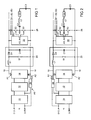
- Fig. 1 shows a schematic representation of the structure of a first embodiment of an electronic control gear according to the invention.
- This has on the input side two poles L, N, wherein the pole L represents a line connection and the pole N is a neutral connection.
- a first sub-filter device 10 to which a second sub-filter device 12 connects.
- the first sub-filter device 10 is optional, wherein in particular switching groups are combined, which have uncompensated chokes and capacitors.
- the second sub-filter device 12 comprises in particular switching groups with transversely arranged capacitors, so-called cross-C, and current-compensated reactors.
- the output of the sub-filter device 12 is coupled to the input of a rectifier 14 whose outputs A1, A2 are coupled to a first voltage rail 16 and a second voltage rail 18, between which a DC voltage is provided.
- a rectifier 14 whose outputs A1, A2 are coupled to a first voltage rail 16 and a second voltage rail 18, between which a DC voltage is provided.
- Fig. 1 is further drawn in an optional voltage converter 20, which comprises an inductance L1, a switch S1, a diode D1 and a capacitor C1.
- the voltage converter is designed as a boost converter. It can also be embodied as a buck converter, as a buck converter and the like, without impairing the invention.
- a monitoring and control device 22 is coupled to supply it between the first voltage rail 16 and the second voltage rail 18. It has three inputs E1 to E3 to monitor a plurality of operating parameters of a discharge lamp La. It also has two outputs A3, A4 in order to control the two switches S2, S3 of a half-bridge circuit of an inverter 26.
- the half-bridge center HM is coupled via the series connection of a capacitor C2 and a lamp inductor L2 to the discharge lamp La. Moreover, a coupling capacitor C3 is provided.
- the discharge lamp La may also be applied to others Be connected manner without excluding the application of the present invention.
- the voltage rail 18 is coupled via a decoupling network 24, which has an input E4 and an output A5, to the neutral terminal.
- the coupling can take place before the first sub-filter device 10 or between the two sub-filter devices 10 and 12.
- the decoupling network comprises a capacitor, not shown, which is serially coupled between the input terminal E4 of the decoupling network 24 and the output terminal A5 of the decoupling network 24.
- Fig. 2 shows a further embodiment of an electronic control gear according to the invention, wherein components corresponding to those of Fig. 1 correspond, are denoted by the same reference numerals and hereinafter only to the differences to Fig. 1 will be received.
- the output E4 of the decoupling network 24 is connected to the first voltage rail 16, while the output A5 is coupled to the line terminal, either before the first filter device 10 or between the first 10 and the second filter device 12th
- the output A5 of the decoupling network 24 is coupled to both marked coupling points.
- the input voltage applied between the line terminal and the neutral terminal can be both an AC voltage as well as a DC voltage.
- the rectifier 14 then acts as reverse polarity protection.
Claims (8)
- Appareil de commande électronique pour faire fonctionner au moins une lampe à décharge (La) comprenant- une borne bipolaire pour connecter l'appareil de commande électronique à une tension d'alimentation, ayant un premier pôle (L) et un deuxième pôle (N) ;- un dispositif de filtrage (10, 12) couplé à la borne bipolaire pour le filtrage des perturbations CEM ;- un redresseur (14), couplé au dispositif de filtrage (10, 12) et ayant une première (A1) et une deuxième borne de sortie (A2), la première borne de sortie (A1) étant couplée à un premier rail de tension (16) pour fournir un premier potentiel de référence et la deuxième borne de sortie (A2) étant couplée à un deuxième rail de tension (18) pour fournir un deuxième potentiel de référence, le redresseur (14) étant conçu pour fournir une tension continue entre sa première (A1) et sa deuxième borne de sortie (A2);- un onduleur (26) avec au moins un premier (S1) et un deuxième commutateur électronique (S2) couplé entre le premier (16) et le deuxième rail de tension (18), le centre de l'onduleur (26) étant couplé à une borne pour ladite au moins une lampe à décharge (La) ; et- un dispositif de surveillance et de commande (22), couplé entre le premier (16) et le deuxième rail de tension (18) et ayant au moins une borne d'entrée pouvant être couplée à ladite au moins une lampe à décharge (La) afin de surveiller au moins un paramètre de fonctionnement de ladite au moins une lampe à décharge (La),caractérisé en ce que
l'appareil de commande électronique comprend en outre précisément un réseau de découplage (24) ayant précisément une borne d'entrée (E4) et au moins une borne de sortie (A5), ladite une borne d'entrée (E4) du réseau de découplage (24) étant reliée à l'un des rails de tension (16, 18) et ladite au moins une borne de sortie (A5) du réseau de découplage (24) étant couplée à l'un des pôles (L, N),
le réseau de découplage (24) comprenant au moins un condensateur, couplé en série entre la borne d'entrée (E4) du réseau de découplage (24) et la au moins une borne de sortie (A5) du réseau de découplage (24),
et le condensateur ayant une capacité comprise entre 1 pF et 1 nF, en particulier entre 10 pF et 100 pF. - Appareil de commande électronique selon la revendication 1,
caractérisé en ce que
le premier pôle (L) constitue une borne Line et le deuxième pôle (N) une borne Neutre. - Appareil de commande électronique selon la revendication 1,
caractérisé en ce que
le premier pôle (L) constitue une borne positive et le deuxième pôle (N) une borne négative. - Appareil de commande électronique selon l'une des revendications précédentes,
caractérisé en ce que
l'appareil de commande électronique est intégré dans un luminaire de classe de protection II. - Appareil de commande électronique selon l'une des revendications précédentes,
caractérisé en ce que
le couplage de ladite au moins une borne de sortie (A5) du réseau de découplage (24) à l'un des pôles (L, N) est situé sur le côté opposé à la borne bipolaire (LN) du dispositif de filtrage (10, 12). - Appareil de commande électronique selon l'une des revendications précédentes,
caractérisé en ce que
le dispositif de filtrage comprend un premier dispositif de filtrage partiel (10) et un deuxième dispositif de filtrage partiel (12) couplés en série entre la borne bipolaire (L, N) et le redresseur (14), le couplage de ladite au moins une borne de sortie (A5) du réseau de couplage (24) à l'un des pôles (L, N) étant situé entre le premier (10) et le deuxième dispositif de filtrage partiel (12). - Appareil de commande électronique selon l'une des revendications précédentes,
caractérisé en ce que
le réseau de découplage (24) est couplé entre l'un des rails de tension (16, 18) et l'un des pôles (L, N) de telle façon qu'au moins une inductance du dispositif de filtrage est shuntée par le réseau de découplage (24). - Appareil de commande électronique selon l'une des revendications précédentes,
caractérisé en ce que
le dispositif de surveillance et de commande (22) est réalisé sous la forme d'un circuit intégré, en particulier sous la forme d'un ASIC.
Priority Applications (1)
| Application Number | Priority Date | Filing Date | Title |
|---|---|---|---|
| PL07820381T PL2191696T3 (pl) | 2007-09-20 | 2007-09-20 | Elektroniczny osprzęt sterujący do sterowania co najmniej jedną lampą wyładowczą |
Applications Claiming Priority (1)
| Application Number | Priority Date | Filing Date | Title |
|---|---|---|---|
| PCT/EP2007/059938 WO2009039879A1 (fr) | 2007-09-20 | 2007-09-20 | Appareil de commande électronique pour faire fonctionner au moins une lampe à décharge |
Publications (2)
| Publication Number | Publication Date |
|---|---|
| EP2191696A1 EP2191696A1 (fr) | 2010-06-02 |
| EP2191696B1 true EP2191696B1 (fr) | 2012-08-29 |
Family
ID=39473782
Family Applications (1)
| Application Number | Title | Priority Date | Filing Date |
|---|---|---|---|
| EP07820381A Not-in-force EP2191696B1 (fr) | 2007-09-20 | 2007-09-20 | Appareil de commande électronique pour faire fonctionner au moins une lampe à décharge |
Country Status (7)
| Country | Link |
|---|---|
| US (1) | US8319453B2 (fr) |
| EP (1) | EP2191696B1 (fr) |
| KR (1) | KR20100061737A (fr) |
| CN (1) | CN101803469B (fr) |
| ES (1) | ES2389454T3 (fr) |
| PL (1) | PL2191696T3 (fr) |
| WO (1) | WO2009039879A1 (fr) |
Family Cites Families (8)
| Publication number | Priority date | Publication date | Assignee | Title |
|---|---|---|---|---|
| US5400241A (en) * | 1992-11-26 | 1995-03-21 | U.S. Philips Corporation | High frequency discharge lamp |
| US5410221A (en) * | 1993-04-23 | 1995-04-25 | Philips Electronics North America Corporation | Lamp ballast with frequency modulated lamp frequency |
| DE4418886A1 (de) * | 1994-05-30 | 1995-12-07 | Patent Treuhand Ges Fuer Elektrische Gluehlampen Mbh | Getaktete Stromversorgung zum Betreiben elektrischer Lampen |
| US5568041A (en) * | 1995-02-09 | 1996-10-22 | Magnetek, Inc. | Low-cost power factor correction circuit and method for electronic ballasts |
| DE19628891C1 (de) * | 1996-07-17 | 1997-07-17 | Hermann Kovacs | Leuchte mit Leistungsversorgungssteuerung für eine Lampe, die auf Berührung eines elektrisch leitenden Teils der Leuchte reagiert |
| EP1107422A3 (fr) * | 1999-12-03 | 2003-08-13 | Heraeus Med GmbH | Procédé pour le fonctionnement d'un éclairage, en particulier pour applications médicales, et éclairage avec une lampe à décharge |
| US6169374B1 (en) * | 1999-12-06 | 2001-01-02 | Philips Electronics North America Corporation | Electronic ballasts with current and voltage feedback paths |
| JP4956019B2 (ja) * | 2005-03-02 | 2012-06-20 | パナソニック株式会社 | 点灯ユニット及びランプ |
-
2007
- 2007-09-20 US US12/679,014 patent/US8319453B2/en not_active Expired - Fee Related
- 2007-09-20 EP EP07820381A patent/EP2191696B1/fr not_active Not-in-force
- 2007-09-20 CN CN2007801006889A patent/CN101803469B/zh not_active Expired - Fee Related
- 2007-09-20 WO PCT/EP2007/059938 patent/WO2009039879A1/fr active Application Filing
- 2007-09-20 PL PL07820381T patent/PL2191696T3/pl unknown
- 2007-09-20 ES ES07820381T patent/ES2389454T3/es active Active
- 2007-09-20 KR KR1020107008588A patent/KR20100061737A/ko not_active Application Discontinuation
Also Published As
| Publication number | Publication date |
|---|---|
| WO2009039879A1 (fr) | 2009-04-02 |
| US8319453B2 (en) | 2012-11-27 |
| CN101803469A (zh) | 2010-08-11 |
| US20100308746A1 (en) | 2010-12-09 |
| PL2191696T3 (pl) | 2013-02-28 |
| CN101803469B (zh) | 2013-07-24 |
| EP2191696A1 (fr) | 2010-06-02 |
| KR20100061737A (ko) | 2010-06-08 |
| ES2389454T3 (es) | 2012-10-26 |
Similar Documents
| Publication | Publication Date | Title |
|---|---|---|
| EP1695434B1 (fr) | Circuit convertisseur comprenant deux convertisseurs partiels | |
| EP0855758B1 (fr) | Circuit pour protection de circuits d'entrée HF de dispositifs de télécommunication | |
| EP1779488B1 (fr) | Filtre de reseau | |
| DE102009029843A1 (de) | Netzfilter und Verwendung eines Netzfilters | |
| EP3556000B1 (fr) | Module d'un convertisseur modulaire multi-niveaux avec court-circuiteur et limiteur de courant du condensateur | |
| DE102018116032B4 (de) | Leistungselektronikeinrichtung | |
| EP0572585B1 (fr) | Dispositif utilise pour faire fonctionner une lampe a decharge | |
| DE102008062133A1 (de) | Elektrisches Filter, insbesondere EMV-Netzfilter | |
| EP0187312B1 (fr) | Circuit de filtrage | |
| EP2191696B1 (fr) | Appareil de commande électronique pour faire fonctionner au moins une lampe à décharge | |
| EP1583403B1 (fr) | Ballast pour au moins une lampe | |
| EP0808084A2 (fr) | Mise hors circuit de sécurité en cas de regime asymétrique | |
| WO2012022555A1 (fr) | Circuit, filtre de réseau, appareil de commande et dispositif d'éclairage ou lampe | |
| DE19814059A1 (de) | Lastseitige Filteranordnung für eine Stromrichter-Schaltungsanordnung | |
| DE102010028448A1 (de) | Schnittstellenschaltung und Verfahren zur Beeinflussung der Flankensteilheit eines Ansteuersignals | |
| DE102008043424A1 (de) | Motoransteuerungsspannungsversorgungsschaltung mit einem EMV-Filter und einem Verpolschutz | |
| DE102018010146A1 (de) | Vorrichtung zur Filterung von hochfrequenten Störspannungen in einer Schaltung zur Leistungsfaktorkorrektur | |
| DE102017106770B4 (de) | Schaltungsanordnung zum Schutz vor Netzüberspannungen für Stromrichter von Fahrzeugen, insbesondere von fahrleitungsgebundenen Fahrzeugen | |
| DE4101963C1 (en) | Protective circuit counteracting mains interference pulses - has compensating capacitor with voltage rising at most to half max. interference voltage | |
| DE10359882A1 (de) | Schaltungsanordnung zum Betreiben von elektrischen Lampen | |
| DE202016103270U1 (de) | Gleichstromschutzschalter mit zwei Kommutierungsteilabschnitten | |
| DE102021211686A1 (de) | Filterschaltung für ein elektrisches Antriebssystem und elektrisches Antriebssystem | |
| EP3095298B1 (fr) | Circuit d'excitation pour une source lumineuse | |
| WO2020148326A1 (fr) | Dispositif de filtrage pour un réseau d'énergie, réseau de filtrage et procédé de fonctionnement d'un dispositif de filtrage | |
| DE102011003182A1 (de) | Vorrichtung zum Unterdrücken harmonischer Oberschwingungen |
Legal Events
| Date | Code | Title | Description |
|---|---|---|---|
| PUAI | Public reference made under article 153(3) epc to a published international application that has entered the european phase |
Free format text: ORIGINAL CODE: 0009012 |
|
| 17P | Request for examination filed |
Effective date: 20100203 |
|
| AK | Designated contracting states |
Kind code of ref document: A1 Designated state(s): AT BE BG CH CY CZ DE DK EE ES FI FR GB GR HU IE IS IT LI LT LU LV MC MT NL PL PT RO SE SI SK TR |
|
| AX | Request for extension of the european patent |
Extension state: AL BA HR MK RS |
|
| 17Q | First examination report despatched |
Effective date: 20101022 |
|
| DAX | Request for extension of the european patent (deleted) | ||
| GRAP | Despatch of communication of intention to grant a patent |
Free format text: ORIGINAL CODE: EPIDOSNIGR1 |
|
| RAP1 | Party data changed (applicant data changed or rights of an application transferred) |
Owner name: OSRAM AG |
|
| GRAS | Grant fee paid |
Free format text: ORIGINAL CODE: EPIDOSNIGR3 |
|
| GRAA | (expected) grant |
Free format text: ORIGINAL CODE: 0009210 |
|
| AK | Designated contracting states |
Kind code of ref document: B1 Designated state(s): AT BE BG CH CY CZ DE DK EE ES FI FR GB GR HU IE IS IT LI LT LU LV MC MT NL PL PT RO SE SI SK TR |
|
| REG | Reference to a national code |
Ref country code: GB Ref legal event code: FG4D Free format text: NOT ENGLISH |
|
| REG | Reference to a national code |
Ref country code: CH Ref legal event code: EP |
|
| REG | Reference to a national code |
Ref country code: AT Ref legal event code: REF Ref document number: 573642 Country of ref document: AT Kind code of ref document: T Effective date: 20120915 |
|
| REG | Reference to a national code |
Ref country code: IE Ref legal event code: FG4D Free format text: LANGUAGE OF EP DOCUMENT: GERMAN |
|
| REG | Reference to a national code |
Ref country code: DE Ref legal event code: R096 Ref document number: 502007010478 Country of ref document: DE Effective date: 20121025 |
|
| REG | Reference to a national code |
Ref country code: ES Ref legal event code: FG2A Ref document number: 2389454 Country of ref document: ES Kind code of ref document: T3 Effective date: 20121026 |
|
| REG | Reference to a national code |
Ref country code: NL Ref legal event code: VDEP Effective date: 20120829 |
|
| REG | Reference to a national code |
Ref country code: LT Ref legal event code: MG4D Effective date: 20120808 |
|
| PG25 | Lapsed in a contracting state [announced via postgrant information from national office to epo] |
Ref country code: CY Free format text: LAPSE BECAUSE OF FAILURE TO SUBMIT A TRANSLATION OF THE DESCRIPTION OR TO PAY THE FEE WITHIN THE PRESCRIBED TIME-LIMIT Effective date: 20120829 Ref country code: LT Free format text: LAPSE BECAUSE OF FAILURE TO SUBMIT A TRANSLATION OF THE DESCRIPTION OR TO PAY THE FEE WITHIN THE PRESCRIBED TIME-LIMIT Effective date: 20120829 Ref country code: IS Free format text: LAPSE BECAUSE OF FAILURE TO SUBMIT A TRANSLATION OF THE DESCRIPTION OR TO PAY THE FEE WITHIN THE PRESCRIBED TIME-LIMIT Effective date: 20121229 |
|
| RAP2 | Party data changed (patent owner data changed or rights of a patent transferred) |
Owner name: OSRAM GMBH |
|
| PG25 | Lapsed in a contracting state [announced via postgrant information from national office to epo] |
Ref country code: GR Free format text: LAPSE BECAUSE OF FAILURE TO SUBMIT A TRANSLATION OF THE DESCRIPTION OR TO PAY THE FEE WITHIN THE PRESCRIBED TIME-LIMIT Effective date: 20121130 Ref country code: LV Free format text: LAPSE BECAUSE OF FAILURE TO SUBMIT A TRANSLATION OF THE DESCRIPTION OR TO PAY THE FEE WITHIN THE PRESCRIBED TIME-LIMIT Effective date: 20120829 Ref country code: PT Free format text: LAPSE BECAUSE OF FAILURE TO SUBMIT A TRANSLATION OF THE DESCRIPTION OR TO PAY THE FEE WITHIN THE PRESCRIBED TIME-LIMIT Effective date: 20121231 Ref country code: SE Free format text: LAPSE BECAUSE OF FAILURE TO SUBMIT A TRANSLATION OF THE DESCRIPTION OR TO PAY THE FEE WITHIN THE PRESCRIBED TIME-LIMIT Effective date: 20120829 Ref country code: SI Free format text: LAPSE BECAUSE OF FAILURE TO SUBMIT A TRANSLATION OF THE DESCRIPTION OR TO PAY THE FEE WITHIN THE PRESCRIBED TIME-LIMIT Effective date: 20120829 |
|
| REG | Reference to a national code |
Ref country code: PL Ref legal event code: T3 |
|
| REG | Reference to a national code |
Ref country code: DE Ref legal event code: R081 Ref document number: 502007010478 Country of ref document: DE Owner name: OSRAM GMBH, DE Free format text: FORMER OWNER: OSRAM AG, 81543 MUENCHEN, DE Effective date: 20130205 |
|
| BERE | Be: lapsed |
Owner name: OSRAM A.G. Effective date: 20120930 |
|
| RAP2 | Party data changed (patent owner data changed or rights of a patent transferred) |
Owner name: OSRAM GMBH |
|
| PG25 | Lapsed in a contracting state [announced via postgrant information from national office to epo] |
Ref country code: CZ Free format text: LAPSE BECAUSE OF FAILURE TO SUBMIT A TRANSLATION OF THE DESCRIPTION OR TO PAY THE FEE WITHIN THE PRESCRIBED TIME-LIMIT Effective date: 20120829 Ref country code: DK Free format text: LAPSE BECAUSE OF FAILURE TO SUBMIT A TRANSLATION OF THE DESCRIPTION OR TO PAY THE FEE WITHIN THE PRESCRIBED TIME-LIMIT Effective date: 20120829 Ref country code: MC Free format text: LAPSE BECAUSE OF NON-PAYMENT OF DUE FEES Effective date: 20120930 Ref country code: RO Free format text: LAPSE BECAUSE OF FAILURE TO SUBMIT A TRANSLATION OF THE DESCRIPTION OR TO PAY THE FEE WITHIN THE PRESCRIBED TIME-LIMIT Effective date: 20120829 Ref country code: NL Free format text: LAPSE BECAUSE OF FAILURE TO SUBMIT A TRANSLATION OF THE DESCRIPTION OR TO PAY THE FEE WITHIN THE PRESCRIBED TIME-LIMIT Effective date: 20120829 Ref country code: EE Free format text: LAPSE BECAUSE OF FAILURE TO SUBMIT A TRANSLATION OF THE DESCRIPTION OR TO PAY THE FEE WITHIN THE PRESCRIBED TIME-LIMIT Effective date: 20120829 |
|
| REG | Reference to a national code |
Ref country code: CH Ref legal event code: PL |
|
| PG25 | Lapsed in a contracting state [announced via postgrant information from national office to epo] |
Ref country code: SK Free format text: LAPSE BECAUSE OF FAILURE TO SUBMIT A TRANSLATION OF THE DESCRIPTION OR TO PAY THE FEE WITHIN THE PRESCRIBED TIME-LIMIT Effective date: 20120829 |
|
| REG | Reference to a national code |
Ref country code: IE Ref legal event code: MM4A |
|
| PLBE | No opposition filed within time limit |
Free format text: ORIGINAL CODE: 0009261 |
|
| STAA | Information on the status of an ep patent application or granted ep patent |
Free format text: STATUS: NO OPPOSITION FILED WITHIN TIME LIMIT |
|
| PG25 | Lapsed in a contracting state [announced via postgrant information from national office to epo] |
Ref country code: LI Free format text: LAPSE BECAUSE OF NON-PAYMENT OF DUE FEES Effective date: 20120930 Ref country code: CH Free format text: LAPSE BECAUSE OF NON-PAYMENT OF DUE FEES Effective date: 20120930 Ref country code: IE Free format text: LAPSE BECAUSE OF NON-PAYMENT OF DUE FEES Effective date: 20120920 Ref country code: BG Free format text: LAPSE BECAUSE OF FAILURE TO SUBMIT A TRANSLATION OF THE DESCRIPTION OR TO PAY THE FEE WITHIN THE PRESCRIBED TIME-LIMIT Effective date: 20121129 Ref country code: BE Free format text: LAPSE BECAUSE OF NON-PAYMENT OF DUE FEES Effective date: 20120930 |
|
| 26N | No opposition filed |
Effective date: 20130530 |
|
| REG | Reference to a national code |
Ref country code: DE Ref legal event code: R097 Ref document number: 502007010478 Country of ref document: DE Effective date: 20130530 |
|
| REG | Reference to a national code |
Ref country code: DE Ref legal event code: R081 Ref document number: 502007010478 Country of ref document: DE Owner name: OSRAM GMBH, DE Free format text: FORMER OWNER: OSRAM GMBH, 81543 MUENCHEN, DE Effective date: 20130823 |
|
| PGFP | Annual fee paid to national office [announced via postgrant information from national office to epo] |
Ref country code: ES Payment date: 20130918 Year of fee payment: 7 |
|
| REG | Reference to a national code |
Ref country code: AT Ref legal event code: MM01 Ref document number: 573642 Country of ref document: AT Kind code of ref document: T Effective date: 20120920 |
|
| PG25 | Lapsed in a contracting state [announced via postgrant information from national office to epo] |
Ref country code: MT Free format text: LAPSE BECAUSE OF FAILURE TO SUBMIT A TRANSLATION OF THE DESCRIPTION OR TO PAY THE FEE WITHIN THE PRESCRIBED TIME-LIMIT Effective date: 20120829 |
|
| PG25 | Lapsed in a contracting state [announced via postgrant information from national office to epo] |
Ref country code: AT Free format text: LAPSE BECAUSE OF NON-PAYMENT OF DUE FEES Effective date: 20120920 |
|
| PG25 | Lapsed in a contracting state [announced via postgrant information from national office to epo] |
Ref country code: TR Free format text: LAPSE BECAUSE OF FAILURE TO SUBMIT A TRANSLATION OF THE DESCRIPTION OR TO PAY THE FEE WITHIN THE PRESCRIBED TIME-LIMIT Effective date: 20120829 |
|
| PG25 | Lapsed in a contracting state [announced via postgrant information from national office to epo] |
Ref country code: LU Free format text: LAPSE BECAUSE OF NON-PAYMENT OF DUE FEES Effective date: 20120920 |
|
| PG25 | Lapsed in a contracting state [announced via postgrant information from national office to epo] |
Ref country code: HU Free format text: LAPSE BECAUSE OF FAILURE TO SUBMIT A TRANSLATION OF THE DESCRIPTION OR TO PAY THE FEE WITHIN THE PRESCRIBED TIME-LIMIT Effective date: 20070920 |
|
| PGFP | Annual fee paid to national office [announced via postgrant information from national office to epo] |
Ref country code: FI Payment date: 20140911 Year of fee payment: 8 |
|
| PGFP | Annual fee paid to national office [announced via postgrant information from national office to epo] |
Ref country code: FR Payment date: 20140919 Year of fee payment: 8 Ref country code: PL Payment date: 20140821 Year of fee payment: 8 Ref country code: GB Payment date: 20140919 Year of fee payment: 8 |
|
| PGFP | Annual fee paid to national office [announced via postgrant information from national office to epo] |
Ref country code: IT Payment date: 20140923 Year of fee payment: 8 |
|
| PG25 | Lapsed in a contracting state [announced via postgrant information from national office to epo] |
Ref country code: IT Free format text: LAPSE BECAUSE OF NON-PAYMENT OF DUE FEES Effective date: 20150920 |
|
| GBPC | Gb: european patent ceased through non-payment of renewal fee |
Effective date: 20150920 |
|
| PG25 | Lapsed in a contracting state [announced via postgrant information from national office to epo] |
Ref country code: FI Free format text: LAPSE BECAUSE OF NON-PAYMENT OF DUE FEES Effective date: 20150920 |
|
| REG | Reference to a national code |
Ref country code: FR Ref legal event code: ST Effective date: 20160531 |
|
| PG25 | Lapsed in a contracting state [announced via postgrant information from national office to epo] |
Ref country code: GB Free format text: LAPSE BECAUSE OF NON-PAYMENT OF DUE FEES Effective date: 20150920 Ref country code: ES Free format text: LAPSE BECAUSE OF NON-PAYMENT OF DUE FEES Effective date: 20140921 |
|
| PG25 | Lapsed in a contracting state [announced via postgrant information from national office to epo] |
Ref country code: FR Free format text: LAPSE BECAUSE OF NON-PAYMENT OF DUE FEES Effective date: 20150930 |
|
| PG25 | Lapsed in a contracting state [announced via postgrant information from national office to epo] |
Ref country code: PL Free format text: LAPSE BECAUSE OF NON-PAYMENT OF DUE FEES Effective date: 20150920 |
|
| PGFP | Annual fee paid to national office [announced via postgrant information from national office to epo] |
Ref country code: DE Payment date: 20190930 Year of fee payment: 13 |
|
| REG | Reference to a national code |
Ref country code: DE Ref legal event code: R119 Ref document number: 502007010478 Country of ref document: DE |
|
| PG25 | Lapsed in a contracting state [announced via postgrant information from national office to epo] |
Ref country code: DE Free format text: LAPSE BECAUSE OF NON-PAYMENT OF DUE FEES Effective date: 20210401 |