EP2189969A2 - Apparatus and method for driving electro-optical device, the electro-optical device, and an electronic apparatus - Google Patents
Apparatus and method for driving electro-optical device, the electro-optical device, and an electronic apparatus Download PDFInfo
- Publication number
- EP2189969A2 EP2189969A2 EP20090175333 EP09175333A EP2189969A2 EP 2189969 A2 EP2189969 A2 EP 2189969A2 EP 20090175333 EP20090175333 EP 20090175333 EP 09175333 A EP09175333 A EP 09175333A EP 2189969 A2 EP2189969 A2 EP 2189969A2
- Authority
- EP
- European Patent Office
- Prior art keywords
- data
- electro
- data lines
- correction voltage
- signal
- Prior art date
- Legal status (The legal status is an assumption and is not a legal conclusion. Google has not performed a legal analysis and makes no representation as to the accuracy of the status listed.)
- Granted
Links
Images


Classifications
-
- G—PHYSICS
- G09—EDUCATION; CRYPTOGRAPHY; DISPLAY; ADVERTISING; SEALS
- G09G—ARRANGEMENTS OR CIRCUITS FOR CONTROL OF INDICATING DEVICES USING STATIC MEANS TO PRESENT VARIABLE INFORMATION
- G09G3/00—Control arrangements or circuits, of interest only in connection with visual indicators other than cathode-ray tubes
- G09G3/20—Control arrangements or circuits, of interest only in connection with visual indicators other than cathode-ray tubes for presentation of an assembly of a number of characters, e.g. a page, by composing the assembly by combination of individual elements arranged in a matrix no fixed position being assigned to or needed to be assigned to the individual characters or partial characters
- G09G3/34—Control arrangements or circuits, of interest only in connection with visual indicators other than cathode-ray tubes for presentation of an assembly of a number of characters, e.g. a page, by composing the assembly by combination of individual elements arranged in a matrix no fixed position being assigned to or needed to be assigned to the individual characters or partial characters by control of light from an independent source
- G09G3/36—Control arrangements or circuits, of interest only in connection with visual indicators other than cathode-ray tubes for presentation of an assembly of a number of characters, e.g. a page, by composing the assembly by combination of individual elements arranged in a matrix no fixed position being assigned to or needed to be assigned to the individual characters or partial characters by control of light from an independent source using liquid crystals
- G09G3/3611—Control of matrices with row and column drivers
- G09G3/3685—Details of drivers for data electrodes
- G09G3/3688—Details of drivers for data electrodes suitable for active matrices only
-
- G—PHYSICS
- G09—EDUCATION; CRYPTOGRAPHY; DISPLAY; ADVERTISING; SEALS
- G09G—ARRANGEMENTS OR CIRCUITS FOR CONTROL OF INDICATING DEVICES USING STATIC MEANS TO PRESENT VARIABLE INFORMATION
- G09G3/00—Control arrangements or circuits, of interest only in connection with visual indicators other than cathode-ray tubes
- G09G3/20—Control arrangements or circuits, of interest only in connection with visual indicators other than cathode-ray tubes for presentation of an assembly of a number of characters, e.g. a page, by composing the assembly by combination of individual elements arranged in a matrix no fixed position being assigned to or needed to be assigned to the individual characters or partial characters
- G09G3/34—Control arrangements or circuits, of interest only in connection with visual indicators other than cathode-ray tubes for presentation of an assembly of a number of characters, e.g. a page, by composing the assembly by combination of individual elements arranged in a matrix no fixed position being assigned to or needed to be assigned to the individual characters or partial characters by control of light from an independent source
- G09G3/36—Control arrangements or circuits, of interest only in connection with visual indicators other than cathode-ray tubes for presentation of an assembly of a number of characters, e.g. a page, by composing the assembly by combination of individual elements arranged in a matrix no fixed position being assigned to or needed to be assigned to the individual characters or partial characters by control of light from an independent source using liquid crystals
- G09G3/3611—Control of matrices with row and column drivers
- G09G3/3614—Control of polarity reversal in general
-
- G—PHYSICS
- G09—EDUCATION; CRYPTOGRAPHY; DISPLAY; ADVERTISING; SEALS
- G09G—ARRANGEMENTS OR CIRCUITS FOR CONTROL OF INDICATING DEVICES USING STATIC MEANS TO PRESENT VARIABLE INFORMATION
- G09G2310/00—Command of the display device
- G09G2310/02—Addressing, scanning or driving the display screen or processing steps related thereto
- G09G2310/0202—Addressing of scan or signal lines
- G09G2310/0218—Addressing of scan or signal lines with collection of electrodes in groups for n-dimensional addressing
-
- G—PHYSICS
- G09—EDUCATION; CRYPTOGRAPHY; DISPLAY; ADVERTISING; SEALS
- G09G—ARRANGEMENTS OR CIRCUITS FOR CONTROL OF INDICATING DEVICES USING STATIC MEANS TO PRESENT VARIABLE INFORMATION
- G09G2310/00—Command of the display device
- G09G2310/02—Addressing, scanning or driving the display screen or processing steps related thereto
- G09G2310/0243—Details of the generation of driving signals
- G09G2310/0248—Precharge or discharge of column electrodes before or after applying exact column voltages
-
- G—PHYSICS
- G09—EDUCATION; CRYPTOGRAPHY; DISPLAY; ADVERTISING; SEALS
- G09G—ARRANGEMENTS OR CIRCUITS FOR CONTROL OF INDICATING DEVICES USING STATIC MEANS TO PRESENT VARIABLE INFORMATION
- G09G2310/00—Command of the display device
- G09G2310/02—Addressing, scanning or driving the display screen or processing steps related thereto
- G09G2310/0264—Details of driving circuits
- G09G2310/0297—Special arrangements with multiplexing or demultiplexing of display data in the drivers for data electrodes, in a pre-processing circuitry delivering display data to said drivers or in the matrix panel, e.g. multiplexing plural data signals to one D/A converter or demultiplexing the D/A converter output to multiple columns
-
- G—PHYSICS
- G09—EDUCATION; CRYPTOGRAPHY; DISPLAY; ADVERTISING; SEALS
- G09G—ARRANGEMENTS OR CIRCUITS FOR CONTROL OF INDICATING DEVICES USING STATIC MEANS TO PRESENT VARIABLE INFORMATION
- G09G2320/00—Control of display operating conditions
- G09G2320/02—Improving the quality of display appearance
- G09G2320/0219—Reducing feedthrough effects in active matrix panels, i.e. voltage changes on the scan electrode influencing the pixel voltage due to capacitive coupling
-
- G—PHYSICS
- G09—EDUCATION; CRYPTOGRAPHY; DISPLAY; ADVERTISING; SEALS
- G09G—ARRANGEMENTS OR CIRCUITS FOR CONTROL OF INDICATING DEVICES USING STATIC MEANS TO PRESENT VARIABLE INFORMATION
- G09G2320/00—Control of display operating conditions
- G09G2320/02—Improving the quality of display appearance
- G09G2320/0233—Improving the luminance or brightness uniformity across the screen
Definitions
- the present invention relates to an apparatus and method for driving an electro-optical device, such as a liquid crystal device, the electro-optical device including the driving apparatus, and an electronic apparatus, for example, a liquid crystal projector, including the electro-optical device.
- an electro-optical device such as a liquid crystal device
- the electro-optical device including the driving apparatus and an electronic apparatus, for example, a liquid crystal projector, including the electro-optical device.
- An electro-optical device controls the orientation of an electro-optical substance (e.g., liquid crystal), which is interposed between a pair of electrodes, by applying a driving voltage corresponding to an image signal between the pair of electrodes to thereby perform image display.
- the driving voltage is applied, with the polarity of the driving voltage being reversed, so as to prevent burn-in or flicker from being created in a displayed image.
- parasitic capacitance occurs between data lines supplied with an image signal to prescribe gradation of pixels and a pixel row connected to the data lines. Display unevenness occurs in the displayed image in a direction along the data line, due to the occurrence of the parasitic capacitance.
- JP-A-2004-45967 discloses a technique for reducing the display unevenness and improving an image quality of a displayed image by changing the order of supplying the image signal to the data line.
- JP-A-2005-43418 discloses a technique for increasing the speed of writing data into the pixels and thus suppressing the display unevenness by overlapping a correction voltage, of which the polarity is reversed compared to the polarity of the driving voltage corresponding to the image signal, with the driving voltage and applying the overlapped correction voltage.
- the display unevenness can be improved to some extent, a lot of display unevenness remains, and the improvement of the image quality is thus required.
- a thin film transistor for switching the control of the timing of applying the driving voltage to, for example, a pixel electrode is exposed to strong light, which results in current leakage.
- the occurrence of light current leakage causes a reduction in the potential of the pixel electrode and increased unevenness in the displayed image.
- An advantage of some aspects of the invention is to provide an apparatus and method for driving an electro-optical device which can prevent or reduce burn-in of a displayed image or flicker, as well as displaying an image at a high quality, an electro-optical device including the driving apparatus, and an electronic apparatus including the electro-optical device.
- an apparatus for driving an electro-optical device including: a plurality of scanning lines; a plurality of data lines that intersect the plurality of scanning lines, and that are divided so that the neighboring data lines form another group of data lines; a plurality of pixels provided to correspond to intersection of the plurality of scanning lines and the plurality of data lines; a data line driving circuit that supplies a correction voltage simultaneously supplied to the group of data lines and having a fixed polarity with respect to a predetermined potential, and a driving voltage time-serially supplied to the group of data lines in response to an image signal and having a polarity that is inverted for each frame with respect to the predetermined potential; and a scanning line driving circuit that supplies a scanning signal through the plurality of scanning lines.
- the scanning signals are sequentially supplied to the plurality of scanning lines by the scanning signal driving circuit.
- the image signals are time-serially supplied to the plurality of data lines by the data line driving circuit.
- the driving voltage corresponding to the image signal is applied to the pixels arranged to correspond to intersection of the plurality of scanning lines and the plurality of data lines.
- the electro-optical operation of, for example, a liquid crystal display is carried out, for example, by changing an orientation state of an electro-optical substance contained in the pixel part and controlling the light transmission rate of each pixel part.
- the driving voltage corresponding to the image signal is applied by driving frame reversion, in which a polarity of the driving voltage is reversed, so that the driving voltage corresponding to the image signal acts on the electro-optical substance interposed between substrates so as to prevent burn-in from occurring in the displayed image.
- the data line driving circuit of the invention applies the driving voltage corresponding to the image signal to the plurality of pixel parts via the plurality of data lines, in which a polarity of the driving voltage with respect to predetermined potential is inversed for every frame.
- the data line driving circuit applies the pulsed correction voltage having a predetermined polarity at least timing ahead of the image signal for every frame.
- the correction voltage is applied ahead of the driving voltage corresponding to the image signal.
- the term "pulsed" means that the correction voltage is shorter than a period of reversing the polarity of the driving voltage, that is, the correction voltage is locally left on a time axis for one reversion period of the driving voltage.
- the pulse of the correction voltage is sufficiently short as compared with the response time of the liquid crystal.
- the correction voltage is different from the driving voltage having the polarity which is reversed for every frame, and has a polarity which is fixed at either positive polarity or a negative polarity during operation of the driving apparatus.
- the driving apparatus for the electro-optical device which is driven by driving frame reversion can reduce the unevenness of a displayed image by applying the correction voltage at the timing ahead of at least the image signal, with the frame being reversed during driving of the apparatus.
- the terms "at least timing ahead of the image signal” and the like mean one timing within a blanking period of vertical scanning or a blanking period of horizontal scanning according to the image signal.
- the term "at least”, a single timing ahead of one image signal for every frame is enough, but the timing ahead of the image signal in each of the plurality of horizontal periods (i.e., a horizontal scanning period) in one frame, that is, plural timing for every frame, may be in effect.
- the correction voltage is generally applied to the plurality of data lines in unison.
- the correction signal is not applied between the pixel electrode and the opposite electrode due to the existence of switching elements or the like, which are in a turned-off state, provided in each pixel part, unlike the image signal (i.e., the driving voltage corresponding thereto).
- the potential of the data line is changed to or approximated to the value of the correction voltage by using a conventional image signal (that is, the driving voltage corresponding thereto) to carry out an electrical task.
- the correction signal is applied between the pixel electrode and the opposite electrode due to the existence of switching elements which are provided in each pixel part and are in a turned-on state, similar to the image signal (that is, the driving voltage corresponding thereto), the period, in which the voltage corresponding to the image signal is held at the pixel electrode, may be regarded as somewhat expendable.
- the potential of the data lines and the pixel electrodes is changed to or approximated to a value of the correction voltage from the value of the image signal (that is, the driving voltage corresponding thereto) to carry out the electrical task.
- the pixel parts which are placed at different areas of an image display region, have parasitic capacitance of different sizes depending upon the transmission distance of driving voltage. For this reason, even if the pixels are connected to the same data line, the value of the driving voltage actually applied to the pixel part is varied.
- the driving apparatus provided in the electro-optical device irradiated by strong light from, for example, a liquid crystal projector, since current leakage is likely to be generated by irradiation of light onto a thin film transistor provided in the driving apparatus in order to control the switching of the pixel electrode, there is a difference between the driving voltages applied between the pixel parts described above.
- the driving apparatus After the image signal is supplied, the driving apparatus according to the invention compensates a potential difference between the plurality of data lines or compensates a difference between the driving voltage values, due to at least the difference between the driving voltage values, and applies the correction voltage to the plurality of data lines at timing ahead of the image signal for every frame. Therefore, it is possible to reduce a difference between the driving voltages supplied or applied via the next data line and produced at the pixel, and thus to the suppress occurrence of the burn-in in the displayed image.
- the correction voltage has a predetermined polarity.
- predetermined polarity means either a positive polarity or a negative polarity. That is, the correction voltage has constantly either a positive polarity or a negative polarity, irrespective of the driving voltage corresponding to the image signal having a polarity which is reversed for every frame.
- the correction voltage according to the invention is a voltage having a property different from that of a so-called pre-charge voltage, of which the polarity is reversed according to the polarity of the driving voltage.
- the correction voltage according to the invention since the correction voltage according to the invention is applied or supplied at timing ahead of the image signal, a kind of pre-charge signal may be perceived as the timing, but the correction voltage having a predetermined polarity (that is, constantly having either the positive polarity or the negative polarity) is different.
- the existing pre-charge signal it is necessary to previously write data with the same polarity as that of the voltage of a next image signal to be written, due to the object of reducing the writing load of the image signal.
- the polarity and intensity of the correction voltage be properly adjusted so as to compensate a voltage of the pixel part which is reduced due to occurrence of current leakage.
- the driving apparatus for the electro-optical device can be arranged to prevent the burn-in of the displayed image and occurrence of flicker, prevent the unevenness on the displayed image and thus enhance the image quality, by applying only the correction voltage at the timing ahead of the pixel signal.
- the data line driving circuit applies the correction voltage to the plurality of data lines at timing ahead of the image signal for each horizontal period in accordance with the image signal in the frame.
- a state, where it is possible to write a pixel placed on one corresponding scanning line, is maintained by supplying a scanning signal to one scanning line, and the correction voltage is applied to the data line for every horizontal period to write the image signal.
- the correction voltage is applied, it is possible to reduce a difference between the driving voltage values, but the difference is enlarged with lapse of time. It is possible to suppress the difference of the driving voltage from being enlarged by applying relatively frequently the correction voltage at a proper time interval.
- the data line driving circuit preferably applies the correction voltage concurrently to the plurality of data lines.
- the correction voltage is simultaneously applied to all of the data lines at the timing ahead of the image signal. Since the timing ahead of the image signal means one timing within a blanking period of vertical scanning or a blanking period of horizontal scanning according to the image signal, it is a period shorter than the horizontal scanning period or the like. Therefore, in order to quickly reduce the difference of the driving voltage with respect to the all of the data lines within a short period, the correction voltage may be concurrently applied to all of the data lines.
- the fixed polarity is preferably a negative polarity.
- the correction voltage overlapped and applied to the driving voltage of the pixel constantly has a negative polarity during operation of the driving apparatus, irrespective of the positive or negative polarity of the driving voltage.
- the driving apparatus for the electro-optical device can be arranged to prevent the burn-in of the displayed image and occurrence of flicker, prevent the unevenness on the displayed image and thus enhance the image quality.
- the correction voltage preferably includes a first correction voltage which is applied with respect to a frame in which the driving voltage has a positive polarity, and a second correction voltage which is applied with respect to a frame in which the driving voltage has a negative polarity.
- the correction voltage overlapped and applied to the driving voltage of the pixel includes the first and second correction voltage, and when the driving voltage having a polarity which is reversed for every frame has either the positive polarity or the negative polarity, the correction voltage is applied by the data line driving circuit. That is, the polarity of the correction voltage is fixed, irrespective of the polarity reversion of the driving voltage, but the amplitude or time width of the first and second correction voltages may be different.
- the concrete amplitude and time width of the first and second correction voltages may be set by properly compensating and adjusting the pixel electrode lowered due to occurrence of the current leakage.
- the data line driving circuit preferably further includes a selection order control unit that applies the driving voltage to the data lines selected from the group of data lines in a predetermined selection order in one horizontal period, in each of the plurality of blocks in which the plurality of data lines are divided, and changes the predetermined selection order on a time axis.
- the plurality of data lines included in the block is selected one by one within one horizontal period. That is, all of the data lines included in the block are selected within one horizontal period.
- the term "predetermined selection order" may include a selection order in which the data lines included in a specified block are selected one by one, a selection order in which the data lines in the block are selected in random order, and a selection order in which all of the data lines in the block are selected within one horizontal period.
- the order (i.e., a predetermined selection order) in which the data lines included in the block are selected may be changed by the selection order control unit. For example, the selection order may be changed every frame, or may be changed for every one horizontal period.
- the driving apparatus for the electro-optical device can be arranged to prevent the burn-in of the displayed image and occurrence of flicker, prevent the unevenness on the displayed image and thus enhance the image quality.
- the selection order control unit may change the specified selection order at least for each frame.
- the burn-in on the charge can be reduced or solved by frequently changing the selection order of the data line for every frame.
- the selection order control unit may change the selection order for each horizontal period.
- the burn-in on the charge can be reduced or solved by frequently changing the selection order of the data line for one horizontal period.
- the burn-in on the charge can be further reduced or solved by frequently changing the selection order.
- a method for driving the electro-optical device including a plurality of scanning lines and a plurality of data lines which intersect in the image display area, and a plurality of pixel parts arranged to correspond to intersection of the plurality of scanning lines and the plurality of data lines, according to the invention, includes supplying the scanning signal via the plurality of scanning lines, applying the driving voltage having a polarity, which is reversed with respect to the predetermined potential for each frame, to the plurality of pixel parts via the plurality of data lines in accordance with the image signal, and applying the pulsed correction voltage having a predetermined polarity at timing ahead of the image signal.
- the driving method according to the invention can arrange the driving of the electro-optical device which can compensate a variation of a response characteristic, similar to the case of the driving apparatus of the invention described above.
- the driving method of the invention can employ various aspects, such as the driving apparatus of the invention described above.
- the electro-optical device includes the driving circuit (in this regard, including various aspects) of the electro-optical device of the invention described above, a pair of substrates, the electro-optical substance interposed between the pair of substrates, and the pixel electrodes arranged to correspond to the intersection of the plurality scanning lines and the plurality of data lines.
- the electro-optical device of the invention includes the driving apparatus of the invention described above, it is possible to display a high quality image in each pixel part, without following the variation of the response characteristic.
- the electro-optical device preferably includes switching elements provided for the respective pixels on one of the pair of substrates, turned on in response to the scanning signal which is supplied from the scanning lines, to supply the image signal supplied from the data lines to the pixel electrodes.
- the data line driving circuit applies the correction voltage in a period immediately before the switching elements are in a turned-on state.
- the electro-optical device includes an element for controlling the switching of the pixel electrode, for example, a thin film transistor, for every pixel part.
- the described-above correction voltage is applied immediately before the switching state is in the turned-on state, in other words, during the turned-off state of the element, the correction voltage is not applied to the pixel electrode. Accordingly, the orientation state of the electro-optical substance interposed between the substrates is not disoriented by the correction voltage.
- the correction voltage has a time width shorter than a response time of the electro-optical substance.
- the orientation state of the electro-optical substance is not affected by the applied correction voltage, and the displayed image is not disoriented. In other words, the correction voltage does not contribute to the gradation display of the image.
- the electro-optical device further includes switching elements provided for the respective pixels on one of the pair of substrates, turned on in response to the scanning signal which is supplied from the scanning lines, to supply the image signal supplied from the data lines to the pixel electrodes.
- the data line driving circuit applies the correction voltage in a period in which the switching elements are in a turned-on state.
- a thin film transistor is provided as a switching element for adjusting the timing in which the voltage is applied to the pixel electrode.
- the correction voltage is applied to the TFT.
- the correction voltage does not affect the orientation state of the electro-optical substance, even though the correction voltage is applied to the data lines and the pixel electrodes.
- the electronic apparatus according to the present invention includes the electro-optical device described-above according to the invention.
- the electronic apparatus of the invention includes the electro-optical device according to the invention, various electronic apparatuses capable of displaying a high quality image, such as a projection-type display device, a cellular phone, an electronic scheduler, a word processor, a viewfinder-type or a monitor-type video tape recorder, a workstation, a television phone, a POS terminal, a touch panel, and so forth, can be achieved.
- the liquid crystal device described includes an electrophoresis apparatus such as an electronic paper.
- Fig. 1 is a block diagram showing an electrical configuration of an electro-optical device according to an embodiment.
- Fig. 2 is a circuit diagram of a switching unit and a driver IC in an electro-optical device according to the embodiment.
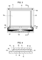
- Fig. 3 is a view schematically showing a detailed configuration around a display unit of an electro-optical device according to the embodiment.
- Fig. 4 is a cross-sectional view taken along the line IV-IV in Fig. 3 .
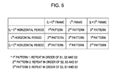
- Fig. 5 is a table showing a driving pattern in each frame of an electro-optical device according to the embodiment.
- Fig. 6 is a timing chart showing the input/output timing of various signals associated with image display in an electro-optical device according to the embodiment.
- Fig. 7 is a timing chart showing waveforms of a driving voltage and a correction voltage in a plurality of sequence frames of an electro-optical device according to the embodiment.
- Fig. 8 is a view schematically showing unevenness occurring in a displayed image in the case where a correction voltage is not applied.
- Fig. 9 is a table showing a relation between amplitude and polarities of a correction voltage in an electro-optical device according to the embodiment, and the size of crosstalk on a displayed image.
- Fig. 10 is a plan view showing a configuration of a projector which is an example of an electronic apparatus to which an electro-optical device is applied.
- a configuration of a liquid crystal apparatus employing a thin film transistor (hereinafter referred to as a TFT) will now be described with reference to Figs. 1 and 2 , which is one example of an electro-optical device including a driving unit for the electro-optical device according to the invention.
- Fig. 1 is a block diagram showing the electrical configuration of the liquid crystal apparatus with respect to each block.
- Fig. 2 is a block diagram showing a detailed circuit configuration of a display unit 1, a signal switching unit 3, a data supply line 7, and a driver IC 5, which are shown in Fig. 1 .
- the display unit 1 is a matrix display unit including pixels of n columns x m rows (n and m are integer numbers), in which a pixel matrix having resolution of m x n is formed by arranging m pixels in an X direction of the matrix wiring and n pixels in a Y direction of the matrix wiring.
- the display unit 1 is connected to the data supply line 7 via the signal switching unit 3, and is supplied with an image signal from the driver IC 5, so that an image corresponding to the image signal is displayed on the display unit 1.
- the display unit 1 is provided with m data lines X (X1, X2, X3, ..., Xm) for supplying the image signal to each pixel, the data lines being divided into k blocks each having three blocks.
- Each block of the data lines X is supplied from the driver IC 5 with the image signal through the data supply line 7.
- an image signal for m pixels arrayed in one horizontal line i.e., the X direction in Figs.
- the liquid crystal device divides all of the data lines X into a plurality of blocks, and drives the image display by performing dot sequential drive in each block (hereinafter referred to as dot sequential drive in block).
- Fig. 3 is a view schematically showing a configuration around the display unit 1 of the liquid crystal device according to the embodiment.
- Fig. 4 is a cross-sectional view taken along the line IV-IV in Fig. 3 .
- a TFT array substrate 10 and an opposite substrate 20 are placed to face each other.
- the TFT array substrate 10 is, for example, a transparent substrate, such as quartz substrate and glass substrate, or a silicon substrate.
- the opposite substrate 20 is a transparent substrate, such as quartz substrate and glass substrate.
- a liquid crystal layer 50 is sealed between the TFT array substrate 10 and the opposite substrate 20.
- the TFT array substrate 10 and the opposite substrate 20 are bonded to each other by a sealing member 52 provided at a sealing area which is around an image display area 10a in which a plurality of pixel electrodes is provided.
- the sealing member 52 is made of, for example, ultraviolet ray curable resin or heat curable resin for bonding both substrates to each other, and is a member that can be obtained as it is cured by ultraviolet rays or heat after the resin is coated on the TFT array substrate 10 in a manufacturing process. Gap members, such as glass fiber or glass beads, are dispersed in the sealing member 52 in order to maintain a predetermined gap (i.e. an inter-substrate gap) between the TFT array substrate 10 and the opposite substrate 20.
- a predetermined gap i.e. an inter-substrate gap
- Aframe-shaped light shielding film 53 of light shielding property which defines a frame-shaped area 10a disposed inside a sealing area, at which the sealing member 52 is placed, is provided on the opposite substrate 20 side. However, part or the entire portion of the frame-shaped light shielding film 53 may be disposed on the TFT array substrate 10 side.
- An external circuit connection terminal 102 is connected to an external circuit for supplying the image signal corresponding to an image to be displayed on the image display area 10a.
- the image signal input to the external connection terminal 102 is processed by a data line driving circuit 101 including the controller 6, the driver IC 5, and the signal switching unit 3, which are shown in Fig. 1 .
- upper and lower conduction terminals 106 for connecting the substrates to each other by interlayer conduction members 107 are placed at positions facing four corners of the opposite substrate 20, respectively. With such a structure, it is possible to enable the TFT array substrate 10 and the opposite substrate 20 to be electrically connected.
- a pixel electrode 9 made of a transparent conductive film, such as ITO (Indium Tin Oxide) film is formed in a matrix shape on the wiring including the TFT for performing the pixel switching or the wiring such as a scanning line and a data line in the pixel display area 10a.
- An aligning film (not shown in Fig. 4 ) is formed on the pixel electrode 9. Meanwhile, a black matrix 23 is formed on the surface of the opposite substrate 20 which is opposite to the TFT array substrate 10.
- the black matrix 23 is made of, for example, a light shield metal film, and is patterned, for example, in a lattice form or a striped form in the image display area 10a over the opposite substrate 20.
- the aligning film is formed on the opposite electrode 21.
- a liquid crystal layer 50 is formed between the TFT array substrate 10 and the opposite substrate 20 placed in such a manner that the pixel electrodes 9 and the opposite electrode 21 face each other and is structured in the above-described manner.
- the liquid crystal layer 50 is made up of liquid crystals in which one kind or several kinds of magnetic liquid crystals are mixed, and the liquid crystals are aligned in a predetermined orientation between the pair of aligning films.
- a pre-charge circuit which supplies a pre-charge signal having a predetermined voltage level to the plurality of data lines before the image signals are supplied to the data lines, a test circuit which tests quality and defects of the electro-optical device which is being manufactured or shipped, an inspection pattern or the like.
- the controller 6 supplies an image signal DATA, a latch timing signal LP, a start signal ST of a shift resistor, a data clock signal CLX, and select signals S1, S2 and S3 to the driver IC 5. Also, the controller 6 supplies a start signal DY of the scanning line driving circuit 4 and a scan clock signal CLY to the scanning line driving circuit 4.
- the driver IC 5 shown in Fig. 1 includes a shift resistor unit 11, first and second latch circuits 12 and 13, and a selector unit 14 and a driver unit 15, which will be described hereinafter in Fig. 2 , a part or all of them may be integrally formed with the display unit 1.
- the controller and the driver IC may be integrally collected, or a part of the function of the controller may be assembled into the driver IC.
- the driver IC 5 includes the shift resistor unit 11, the first latch circuit 12, the second latch circuit 13, the selector unit 14, and the driver unit 15.
- the driver unit 15 of the driver IC 5 is connected to the signal switching unit 3 via the data supply line 7 which transmits the converted image signal for each block.
- the shift resistor unit 11 is input with the data clock signal CLX and the start signal ST.
- the start signal ST is shifted in order into the shift resistor unit 11 in synchronization with the data clock signal CLX.
- the output signal from each unit resistor of the shift resistor unit 11 is respectively input to one of plural unit latch circuits constituting the first latch circuit 12.
- the image signal DATA which is an image signal is simultaneously supplied to all unit latch circuits of the first latch circuit 12. If an output signal is input from the unit resistor, the image signals DATA are accumulated in each unit latch circuit of the first latch circuit 12 by turns.
- the m image signals DATA for one line, that is, for one horizontal scanning line, are accumulated in the first latch circuit 12.
- the image signal DATA is, for example, 6-bit digital signal.
- the second latch circuit 13 is a circuit for latching the image signal DATA of the first latch circuit 12 intact in accordance with a latch timing signal LP. Accordingly, m data for one line are simultaneously latched in the second latch circuit 13.
- Each of the latch circuits 13(1), 13(2), ..., and 13(m) of the second latch circuit 13 latches the image signal corresponding to the data lines X1, X2, ..., and Xm.
- the selector unit 14 includes a plurality of select circuits 14(1), 14(2), ..., and 14(k).
- a plurality of groups is formed by dividing the image signals DATA for one line into data corresponding to three pixels which are consecutive from the start or the end of the data for one line. Three data of each group are input to each corresponding select circuit 14(k). More specifically, the select circuit 14(1) is input by 1, 2 and 3 image signals DATA, the select circuit 14(2) is input by 4, 5 and 6 image signals DATA, and the select circuit 14(k) is input by (m-2), (m-1) and m image signals DATA.
- the selector unit 14 is supplied by the select signals S1, S2 and S3, and each select circuit 14(k) selects one previously predetermined image data among three input image data in accordance with the select signals S1, S2 and S3, and supplies the selected image data to the driver circuit corresponding to the driver unit 15 as an output signal.
- the driver unit 15 includes the plurality of drive circuits 15(1), 15(2), ..., 15(k). For example, when the select signal S1 is supplied, the select circuit 14(1) outputs the image signal DATA1 to the driver circuit 15(1), the select circuit 14(2) outputs the image signal DATA4 to the driver circuit 15(2), and the select circuit 14(k) outputs the image signal DATA(m-2) to the driver circuit 15(k).
- Each drive circuit 15 is a circuit including, for example, a digital-to-analog converter, an amplification circuit or the like.
- the image signal DATA analog-converted by each driver circuit 15 is supplied to the signal switching unit 3 via the k data supply lines 7.
- the signal switching unit 3 includes a plurality of signal switching circuits 3(1), 3(2), ..., 3(k). Each signal switching circuit has three switch circuits SW1, SW2 and SW3. The image signal DATA supplied from each driver circuit is supplied to one end of three switch circuits SW1, SW2 and SW3 of the corresponding signal switching circuit. The other end of each switch circuit which is an output is connected to the corresponding data lines X1, X2, ..., and Xm of the data line group in a direction X of the pixel 2.
- the signal switching unit 3 is supplied by the select signals S1, S2 and S3 for turning the each switch circuit on or off.
- Each of the switch circuits SW1, SW2 and SW3 of the signal switching unit 3 is selectively sequentially turned on in accordance with the select signals S1, S2 and S3, and time-serially supplies the image signal DATA to the corresponding data line from the corresponding drive circuit.
- the switch circuit SW1 of the signal switching circuit 3(1) when the select signal S1 to turn on the switch circuit SW1 is supplied, the switch circuit SW1 of the signal switching circuit 3(1) is turned on, and the image signal corresponding to the image signal DATA1 is output to the data line X1.
- the switch circuit SW1 of the signal switching circuit 3(2) is turned on, and the image signal corresponding to the image signal DATA4 is output to the data line X4.
- the switch circuit SW1 of the signal switching circuit 3(k) is turned on, and the image signal corresponding to the image signal DATA(m-2) is output to the data line X(m-2).
- the switch circuit SW2 of the signal switching circuit 3(1) when the select signal S2 to turn on the switch circuit SW2 is supplied, the switch circuit SW2 of the signal switching circuit 3(1) is turned on, and the image signal corresponding to the image signal DATA2 is output to the data line X2.
- the switch circuit SW2 of the signal switching circuit 3(2) is turned on, and the image signal corresponding to the image signal DATA5 is output to the data line X5.
- the switch circuit SW2 of the signal switching circuit 3(k) is turned on, and the image signal corresponding to the image signal DATA(m-1) is output to the data line X(m-1).
- the switch circuit SW3 of the signal switching circuit 3(1) When the select signal S3 to turn on the switch circuit SW3 is supplied, the switch circuit SW3 of the signal switching circuit 3(1) is turned on, and the image signal corresponding to the image signal DATA3 is output to the data line X3. Similarly, the switch circuit SW3 of the signal switching circuit 3(2) is turned on, and the image signal corresponding to the image signal DATA6 is output to the data line X6. Similarly, the switch circuit SW3 of the signal switching circuit 3(k) is turned on, and the image signal corresponding to the image signal DATAm is output to the data line Xm.
- each signal switching circuit is switched by turning on the predetermined switching circuits SW1, SW2 and SW3 in accordance with the select signals S1, S2 and S3 to sequentially select the image signal from each drive circuit 15 and output the selected image signal to the corresponding data line.
- Each of the switch circuits SW1, SW2 and SW3 is sequentially turned on in one horizontal period (that is, in a horizontal scan period), and the image signal is supplied to all of the data lines in all blocks in one horizontal period. Accordingly, dot sequential drive is performed for every block constituted by three data lines.
- the embodiment is constructed so as to alter the order of turning on the switch circuits SW1, SW2 and SW3 on a time axis, for example, for every line, by adjusting the timing at which the select signals S1 to S3 are output from the controller 6.
- the switch circuits SW1, SW2 and SW3 are sequentially turned on in the order of the switch circuits SW1, SW2 and SW3 in any one horizontal period by the select signals S1 to S3, where the image signal is first supplied to the data lines X1, X4, X7, extended, the image signal is then supplied to the data lines X2, X5, X8,mitted, and finally the image signal is supplied to the data lines X3, X6, X9,mitted.
- the image signal can then be first supplied to the data lines X2, X5, X8,mitted, the image signal can be supplied to the data lines X1, X4, X7, extended, and finally the image signal can be supplied to the data lines X3, X6, X9,mitted.
- the embodiment is constructed so as to alter the order of turning on the switch circuits SW1, SW2 and SW3 for every horizontal period. More specifically, as shown in Fig. 5 , a first pattern (S1, S2, S3), a second pattern (S2, S3, S1) and a third pattern (S3, S1, S2) are alternatively altered for every horizontal period in three consecutive frame periods by the controller 6.
- Fig. 6 is a timing chart showing an input/output timing of each signal in the above-described circuit configuration.
- Fig. 6 depicts the timing chart of a start pulse St, a data clock signal CLX, a latch timing signal LP, the select signals S1, S2 and S3, and scan signals Y(L-1) and Y(L) for respective lines in the circuit configuration shown in Fig. 2 .
- the image signals DATA1, DATA2, ..., and DATAm corresponding to each pixel are supplied to the first latch circuit 12 at a transmission rate corresponding to the data clock CLX.
- the start pulse ST shifts sequentially the shift resister unit 11 in response to the data clock CLX, which supplies a latch pulse to latch each pixel of the first latch circuit 12. Therefore, each unit latch latches sequentially the image signals DATA1, DATA2, ..., and DATAm corresponding to each pixel of horizontal direction of the pixel unit 2.
- the image signals DATA1, DATA2, ..., and DATAm for one line of the first latch circuit 12 are latched to the second latch circuit 13 at the timing of the latch timing signal LP, and the latched data is output.
- the image data for one line output from the second latch circuit 13 is written into each pixel electrode of the scanning line which is turned on by the gate signal, within one horizontal period.
- the scanning line of the (L-1) th line in the n th column that is, the (L-1) th horizontal period
- the scanning line corresponding to the scanning signal Y(L-1) of a signal waveform shown in Fig. 6 is output.
- the scanning line Y (L-1) is set to a high level (hereinafter referred to as HIGH) while the image data DATA is applied to the data line.
- the scanning signal Y (L-1) is a high level immediately after a pulsed correction voltage having a negative polarity which will be described hereinafter is input.
- the scanning signal Y Since the scanning signal Y becomes a high level at such timing, it prevents the displayed image from being distorted by directly applying the correction voltage to the pixel electrode.
- the scanning signal Y may be set to a high level before the correction voltage is input, since in this case the displayed image is hardly distorted even though the correction voltage is applied to the pixel electrode.
- the image data for one pixel from the second latch circuit 13 is divided into k neighboring blocks each having three pixels, and the image data for one pixel of each block is selected by the select circuits 14(1), 14(2), ..., and 14(k).
- the selection is performed on the basis of the selection signals S1, S2 and S3.
- the select signals S1, S2 and S3 are signals which become HIGH only in about 1/3 period of one horizontal period, as shown in Fig. 4 .
- the select circuits 14(1), 14(2), ..., and 14(k) select the image data for one pixel of each group according to the HIGH state of the select signals S1, S2 and S3.
- the select circuits 14(1), 14(2), ..., and 14(k) select and output the image signals DATA1, DATA4, DATA7, extended of the pixels (1), (4), (7), covered according to the HIGH state of the select signal S1, select and output the image signals DATA2, DATA5, DATA8, defined of the pixels (2), (5), (8), covered according to the HIGH state of the select signal S2, and select and output the image signals DATA3, DATA6, DATA9, extended of the pixels (3), (6), (9), covered according to the HIGH state of the select signal S3.
- the image data from the select circuit 14(1), 14(2), ..., and 14(k) are converted into analog signals and amplified by the drive circuits 15(1), 15(2), ..., 15(k), and then are supplied to the signal switching circuits 3(1), 3(2), ..., 3(k).
- the signal switching circuits 3(1), 3(2), ..., and 3(k) branch the input image data to the data lines X1, X2,mitted, respectively.
- the signal switching circuits 3(1), 3(2), ..., and 3(k) are controlled by the select signals S1, S2 and S3 to output one input to one of three outputs.
- the signal switching circuits 3(1), 3(2), ..., and 3(k) output the image data to the first output among three outputs during the HIGH state of the select signal S1, output the image data to the second output among three outputs during the HIGH state of the select signal S2, and output the image data to the third output among three outputs during the HIGH state of the select signal S3.
- the image data selected by the select circuits 14(1), 14(2), ..., and 14(k) are supplied to the data lines X1, X4, X7,mitted.
- the select signal S2 is HIGH
- the image data selected by the select circuits 14(1), 14(2), ..., and 14(k) are supplied to the data lines X2, X5, X8,mitted.
- the select signal S3 is HIGH
- the image data selected by the select circuits 14(1), 14(2), ..., and 14(k) are supplied to the data lines X3, X6, X9,mitted.
- the image signal DATA1, DATA4, DATA7, are supplied to the data lines X1, X4, X7, covered according to the HIGH state of the select signal S1.
- the scanning signal YL-1 becomes HIGH, and each of the 1 st , 4 th , 7 th , mandatory th TFTs 30 of the scanning line L-1 is supplied by the image signals DATA1, DATA4, DATA7, extended via the data lines X1, X4, X7,mitted.
- the writing of the data into the pixel electrode is performed until the (L-1) th horizontal period is terminated.
- the image signal DATA2, DATA5, DATA8, are supplied to each of the 2 nd , 5 th , 8 th , extended th TFTs 30 of the scanning line L-1 via the data lines X2, X5, X8,mitted according to the HIGH state of the select signal S2. After that, the writing of the data into the pixel electrode is performed until the (L-1) th horizontal period is terminated.
- the image signal DATA3, DATA6, DATA9, mandatory are supplied to each of the 3 rd , 6 th , 9 th , extended th TFTs 30 of the scanning line L-1 via the data lines X3, X6, X9, specified according to the HIGH state of the select signal S3.
- the writing of the data into the pixel electrode is performed until the (L-1) th horizontal period is terminated.
- a writing period for writing data into the pixel electrode via the data lines X1, X4, X7, extended is an about 1H (horizontal) period
- a writing period for writing data into the pixel electrode via the data lines X2, X5, X8,mitted is an about (2/3)H period
- a writing period of writing data into the pixel electrode via the data lines X3, X6, X9,mitted is an about (1/3)H period.
- the image data selected on the basis of the select signals S1, S2 and S3 are supplied to the corresponding to data line, and are written into the pixel electrode via the TFT 16 which is turned on.
- the order of the data lines performing the writing of the image data is set to be different from that of the (L-1) th horizontal period.
- the select signal S3 becomes HIGH in the first approximately 1/3 period of one horizontal period
- the select signal S1 becomes HIGH in the next approximately 1/3 period
- the select signal S2 becomes HIGH in the final approximately 1/3 period.
- the writing of the data into the pixel electrode through the data line X3, X6, X9, extended is performed during the about 1H period from the beginning of the L th horizontal period
- the writing of the data into the pixel electrode via the data line X1, X4, X7, extended is performed during the about (2/3)H period on the way of the L th horizontal period
- the writing of the data into the pixel electrode via the data lines X2, X5, X8,mitted is performed during the about (1/3)H period at the last of the L th horizontal period.
- the select signal S2 becomes HIGH in the first approximately 1/3 period of one horizontal period, the select signal S3 becomes HIGH in the next approximately 1/3 period, and the select signal S1 becomes HIGH in the final approximately 1/3 period.
- the writing of the data into the pixel electrode through the data line X2, X5, X8,mitted is performed during approximately 1H period from the beginning of the (L+1) th horizontal period
- the writing of the data into the pixel electrode via the data line X3, X6, X9, extended is performed during approximately the (2/3)H period on the way of the (L+1) th horizontal period
- the writing of the data into the pixel electrode via the data lines X1, X4, X7, extended is performed during approximately the (1/3)H period at the last of the (L+1) th horizontal period.
- the select signals S1, S2 and S3 repeat the same pattern in a cycle of three horizontal periods.
- the writing period of writing the data into each pixel electrode is equal to those of the others in any data lines. Therefore, since luminance unevenness occurring in each line is equalized every three lines, it is possible to display the image with no luminance unevenness on the whole.
- the timing of supplying the image data to each data line in the block is switched for every line, and the writing period of writing the data into the pixel electrode is equalized by the plurality of lines. Therefore, luminance variation in the screen due to the writing period is averaged for the plurality of lines by distribution between the pixels of the same luminance, so that it is difficult to see the display unevenness.
- the writing period of the pixel electrode is equalized in the three horizontal periods.
- the time period of equalizing the writing period is not limited to three horizontal periods.
- the developmental pattern of the select signal is not limited to that shown in Fig. 5 , and may be changed in various shapes.
- the developmental pattern of the select signals S1 and S3 may be changed in a cycle of one horizontal period.
- the writing period of all pixels may be equalized in two horizontal periods. In other words, if the developmental pattern of the select signals S1, S2 and S3 is changed on the time axis, the writing period of the pixel may be again equalized.
- the HIGH period of the select signals is set to a time shorter than 1/3 time of one horizontal period, similar to the case where the driving performance of the drive circuit is high, even though timing of generating any one of the select signals S1, S2 and S3 is changed, some effects can be obtained.
- Fig. 7 is a timing chart of outputting the image signal DATA including the latch timing signal LP, the select signals S1, S2 and S3, and the correction voltage over three consecutive frame periods (that is, a (M-1) th frame period, an M th frame period, and a (M+1) th frame period).
- Fig. 7 shows concrete waveforms of the image signals DATA including the correction voltage.
- the correction voltage is indicated by an arrow in Fig. 7 , and the waveforms which are not indicated by the arrow show the waveforms of the image signals DATA according to the displayed image.
- the pulsed correction voltage having a negative polarity is applied with respect to reference potential of the image signal DATA. That is, the pulsed correction voltage is overlapped and applied to the driving voltage corresponding to the image signal. Also, the time width of the correction voltage is set to be short in comparison with the voltage response time of liquid molecules constituting the liquid crystal layer which is sandwiched between the substrates (typically, the TFT array substrate and the opposite substrate) in the liquid crystal apparatus.
- the driving voltage applied to the liquid crystal layer that is, the image signal DATA, applied according to the displayed image is applied while the polarity is reversed for every frame period.
- the image signal DATA of a negative polarity is applied with respect to the reference voltage (indicated by a dotted line in Fig. 7 ) in the (M-1) th frame period.
- the negative polarity is reversed to a positive polarity with respect to the reference voltage in the next M th frame period.
- the positive polarity is reversed to the negative polarity with respect to the reference voltage in the next (M+1) th frame period.
- the correction voltage V overlapped and applied to the image signal DATA constantly has a negative polarity with respect to the reference voltage from the (M-1) th frame period to the (M+1) th frame period.
- the applied correction voltage V (hereinafter referred to as a first correction voltage V1) has the same amplitude.
- the applied correction voltage V (hereinafter referred to as a second correction voltage V2) has an amplitude different from that of the first correction voltage V1. That is, the overlapped and applied correction voltage V1 is set to have a different magnitude depending on the polarity of the image signal DATA.
- the first correction voltage V1 and the second correction voltage V2 are applied to all of the data lines, before the image signal DATA is supplied in each frame period.
- the select signals S1, S2 and S3 are set to reach a high level by the controller 6 at the timing in which the first correction voltage V1 and the second correction voltage V2 are supplied.
- the driving apparatus for the electro-optical device can reduce the unevenness of displayed image by applying the correction voltage V at timing ahead of the image signal DATA, with the frame being reversed during driving of the apparatus.
- V the correction voltage
- a and B portions should be displayed at the same luminance, but if the correction voltage is not applied, there is a difference between the luminance of the A portion and the luminance of the B portion, as shown in Fig. 8 , so that the display unevenness occurs.
- Fig. 8 is a view schematically showing the unevenness occurring in a displayed image in the case where a correction voltage is not applied.
- a specified driving voltage is applied to the data lines connected to the pixel placed in a section (a) so as to display the pixel in black. Since it is preferable that the data line connected to the pixel contained in a section (b) be displayed in white, the driving voltage is not applied to the data lines placed in the section, or the driving voltage which is significantly lower than that of section (a) is applied.
- the data lines connected to the corresponding to pixel in section (a) are applied with a high driving voltage, similar to the pixels placed over the dotted line indicated by the reference numeral (1), in comparison with section (b).
- the display unevenness occurs, as shown in Fig. 8 .
- the driving apparatus mounted in the electro-optical device irradiated by strong light for example, current leakage is likely generated by irradiating light onto the thin film transistor 30, provided in the driving apparatus, for controlling the switching of the pixel electrode, and the display unevenness may easily occur, as described above. If there is a difference between the driving voltages applied to each pixel, display unevenness, that is, crosstalk, occurs on the displayed image, which causes reduction in image quality.
- Fig. 9 is a table showing results by measuring the size of the crosstalk on the displayed image with respect to a variation between the amplitude of the first correction voltage V1 and the amplitude of the second correction voltage V2.
- the amplitude of the first correction voltage V1 was set to -4 V, while the amplitude of the second correction voltage V2 was varied.
- the correction voltages V1 and V2 be voltages within the amplitude of the image data having the negative polarity, that is, a voltage between the maximum voltage and the minimum voltage in the image data having the negative polarity.
- the driving apparatus for the electro-optical device can be arranged to prevent the burn-in of the displayed image and occurrence of flicker, prevent the unevenness on the displayed image and thus enhance the image quality by applying correction voltage V at the timing ahead of the pixel signal DATA.
- the invention may be applied to the case where the signal switching circuit is provided for a block in which the plurality of scanning lines are divided into other numbers (e.g., 4, 8, 12, 16, or the like).
- FIG. 10 is a plan view showing an exemplified structure of a projector.
- a projector in which the liquid crystal device is used as a light valve will be described.
- each of the liquid crystal panels 1110R, 1110B, and 1110G is the same as the above-described liquid crystal device and is driven by any of primary color signals R, G, and B supplied from the image signal processing circuit.
- the light modulated by these liquid crystal panels enters a dichroic prism 1112 in three directions.
- the R and B light components are reflected at an angle of 90°C, but G light component progresses straight. Accordingly, all color components of the image are synthesized and therefore the color image, such as a screen, is projected via a projection lens 1114.
- an image displayed by the liquid crystal panel 1110G must be reversed right and left with respect to the images displayed by the liquid crystal panels 1110R and 1110B.
- the electro-optical device according to the invention also can be applied to a mobile-type personal computer, a cellular phone, a liquid crystal television, a viewfinder-type or a monitor-type video tape recorder, a car navigation device, a pager, an electronic scheduler, a calculator, a word processor, a workstation, a television phone, a POS terminal, and apparatuses with a touch panel.
- the invention can be applied to a reflective liquid crystal device (LCOS), a plasma display (PDP), an electric field emission display (FED, SED), an organic electroluminescence display, a digital micro-mirror device (DMD), and an electrophoresis display.
- LCOS reflective liquid crystal device
- PDP plasma display
- FED electric field emission display
- SED organic electroluminescence display
- DMD digital micro-mirror device
- the invention is not limited to the above-mentioned embodiments and can be modified as long as it does not conflict with the scope of the invention construed from the claims and specification.
- the electro-optical device accompanied with the modifications, a substrate for the electro-optical device, and the electronic apparatus including the electro-optical device will be within the technical scope of the invention.
Landscapes
- Engineering & Computer Science (AREA)
- Chemical & Material Sciences (AREA)
- Crystallography & Structural Chemistry (AREA)
- Physics & Mathematics (AREA)
- Computer Hardware Design (AREA)
- General Physics & Mathematics (AREA)
- Theoretical Computer Science (AREA)
- Control Of Indicators Other Than Cathode Ray Tubes (AREA)
- Liquid Crystal Display Device Control (AREA)
- Liquid Crystal (AREA)
Abstract
Description
- The present invention relates to an apparatus and method for driving an electro-optical device, such as a liquid crystal device, the electro-optical device including the driving apparatus, and an electronic apparatus, for example, a liquid crystal projector, including the electro-optical device.
- An electro-optical device controls the orientation of an electro-optical substance (e.g., liquid crystal), which is interposed between a pair of electrodes, by applying a driving voltage corresponding to an image signal between the pair of electrodes to thereby perform image display. The driving voltage is applied, with the polarity of the driving voltage being reversed, so as to prevent burn-in or flicker from being created in a displayed image. In particular, parasitic capacitance occurs between data lines supplied with an image signal to prescribe gradation of pixels and a pixel row connected to the data lines. Display unevenness occurs in the displayed image in a direction along the data line, due to the occurrence of the parasitic capacitance.
-
JP-A-2004-45967 JP-A-2005-43418 - However, according to the above-described background art, although the display unevenness can be improved to some extent, a lot of display unevenness remains, and the improvement of the image quality is thus required. For example, in an electro-optical device equipped in an apparatus, such as a liquid crystal projector, a thin film transistor for switching the control of the timing of applying the driving voltage to, for example, a pixel electrode is exposed to strong light, which results in current leakage. In other words, there is a problem that the occurrence of light current leakage causes a reduction in the potential of the pixel electrode and increased unevenness in the displayed image.
- An advantage of some aspects of the invention is to provide an apparatus and method for driving an electro-optical device which can prevent or reduce burn-in of a displayed image or flicker, as well as displaying an image at a high quality, an electro-optical device including the driving apparatus, and an electronic apparatus including the electro-optical device.
- According to an aspect of the invention, there is provided an apparatus for driving an electro-optical device, including: a plurality of scanning lines; a plurality of data lines that intersect the plurality of scanning lines, and that are divided so that the neighboring data lines form another group of data lines; a plurality of pixels provided to correspond to intersection of the plurality of scanning lines and the plurality of data lines; a data line driving circuit that supplies a correction voltage simultaneously supplied to the group of data lines and having a fixed polarity with respect to a predetermined potential, and a driving voltage time-serially supplied to the group of data lines in response to an image signal and having a polarity that is inverted for each frame with respect to the predetermined potential; and a scanning line driving circuit that supplies a scanning signal through the plurality of scanning lines.
- With the apparatus for driving the electro-optical device according to the invention, if various signals, such as a power signal, a data signal, and a control signal, are input or output during operation, the scanning signals are sequentially supplied to the plurality of scanning lines by the scanning signal driving circuit. Simultaneously, the image signals are time-serially supplied to the plurality of data lines by the data line driving circuit. As a result, the driving voltage corresponding to the image signal is applied to the pixels arranged to correspond to intersection of the plurality of scanning lines and the plurality of data lines. The electro-optical operation of, for example, a liquid crystal display is carried out, for example, by changing an orientation state of an electro-optical substance contained in the pixel part and controlling the light transmission rate of each pixel part. The driving voltage corresponding to the image signal is applied by driving frame reversion, in which a polarity of the driving voltage is reversed, so that the driving voltage corresponding to the image signal acts on the electro-optical substance interposed between substrates so as to prevent burn-in from occurring in the displayed image.
- In particular, the data line driving circuit of the invention applies the driving voltage corresponding to the image signal to the plurality of pixel parts via the plurality of data lines, in which a polarity of the driving voltage with respect to predetermined potential is inversed for every frame. Also, the data line driving circuit applies the pulsed correction voltage having a predetermined polarity at least timing ahead of the image signal for every frame. In other words, the correction voltage is applied ahead of the driving voltage corresponding to the image signal. As used herein, the term "pulsed" means that the correction voltage is shorter than a period of reversing the polarity of the driving voltage, that is, the correction voltage is locally left on a time axis for one reversion period of the driving voltage. Accordingly, the pulse of the correction voltage is sufficiently short as compared with the response time of the liquid crystal. The correction voltage is different from the driving voltage having the polarity which is reversed for every frame, and has a polarity which is fixed at either positive polarity or a negative polarity during operation of the driving apparatus.
- According to studies of the inventors, it was proved by way of experiment that the driving apparatus for the electro-optical device which is driven by driving frame reversion can reduce the unevenness of a displayed image by applying the correction voltage at the timing ahead of at least the image signal, with the frame being reversed during driving of the apparatus. As used herein, the terms "at least timing ahead of the image signal" and the like mean one timing within a blanking period of vertical scanning or a blanking period of horizontal scanning according to the image signal. For example, the term "at least", a single timing ahead of one image signal for every frame is enough, but the timing ahead of the image signal in each of the plurality of horizontal periods (i.e., a horizontal scanning period) in one frame, that is, plural timing for every frame, may be in effect. Also, in the case where plural frames are regarded as one time unit, timing only ahead of the image signal to be applied within the corresponding time unit may be possible. Differently from the image signal, the correction voltage is generally applied to the plurality of data lines in unison.
- The correction signal is not applied between the pixel electrode and the opposite electrode due to the existence of switching elements or the like, which are in a turned-off state, provided in each pixel part, unlike the image signal (i.e., the driving voltage corresponding thereto). The potential of the data line is changed to or approximated to the value of the correction voltage by using a conventional image signal (that is, the driving voltage corresponding thereto) to carry out an electrical task. Otherwise, even though the correction signal is applied between the pixel electrode and the opposite electrode due to the existence of switching elements which are provided in each pixel part and are in a turned-on state, similar to the image signal (that is, the driving voltage corresponding thereto), the period, in which the voltage corresponding to the image signal is held at the pixel electrode, may be regarded as somewhat expendable. However, the potential of the data lines and the pixel electrodes is changed to or approximated to a value of the correction voltage from the value of the image signal (that is, the driving voltage corresponding thereto) to carry out the electrical task.
- In the electro-optical device equipped with the driving apparatus according to the invention, the pixel parts, which are placed at different areas of an image display region, have parasitic capacitance of different sizes depending upon the transmission distance of driving voltage. For this reason, even if the pixels are connected to the same data line, the value of the driving voltage actually applied to the pixel part is varied. In the driving apparatus provided in the electro-optical device irradiated by strong light from, for example, a liquid crystal projector, since current leakage is likely to be generated by irradiation of light onto a thin film transistor provided in the driving apparatus in order to control the switching of the pixel electrode, there is a difference between the driving voltages applied between the pixel parts described above. After the image signal is supplied, the driving apparatus according to the invention compensates a potential difference between the plurality of data lines or compensates a difference between the driving voltage values, due to at least the difference between the driving voltage values, and applies the correction voltage to the plurality of data lines at timing ahead of the image signal for every frame. Therefore, it is possible to reduce a difference between the driving voltages supplied or applied via the next data line and produced at the pixel, and thus to the suppress occurrence of the burn-in in the displayed image.
- According to the invention, in particular, the correction voltage has a predetermined polarity. As used herein, the term "predetermined polarity" means either a positive polarity or a negative polarity. That is, the correction voltage has constantly either a positive polarity or a negative polarity, irrespective of the driving voltage corresponding to the image signal having a polarity which is reversed for every frame. In this regard, the correction voltage according to the invention is a voltage having a property different from that of a so-called pre-charge voltage, of which the polarity is reversed according to the polarity of the driving voltage. That is, since the correction voltage according to the invention is applied or supplied at timing ahead of the image signal, a kind of pre-charge signal may be perceived as the timing, but the correction voltage having a predetermined polarity (that is, constantly having either the positive polarity or the negative polarity) is different. In the case of the existing pre-charge signal, it is necessary to previously write data with the same polarity as that of the voltage of a next image signal to be written, due to the object of reducing the writing load of the image signal.
- It is preferable that the polarity and intensity of the correction voltage be properly adjusted so as to compensate a voltage of the pixel part which is reduced due to occurrence of current leakage.
- As described above, the driving apparatus for the electro-optical device can be arranged to prevent the burn-in of the displayed image and occurrence of flicker, prevent the unevenness on the displayed image and thus enhance the image quality, by applying only the correction voltage at the timing ahead of the pixel signal.
- Preferably, the data line driving circuit applies the correction voltage to the plurality of data lines at timing ahead of the image signal for each horizontal period in accordance with the image signal in the frame.
- According to the invention, a state, where it is possible to write a pixel placed on one corresponding scanning line, is maintained by supplying a scanning signal to one scanning line, and the correction voltage is applied to the data line for every horizontal period to write the image signal. As described above, if the correction voltage is applied, it is possible to reduce a difference between the driving voltage values, but the difference is enlarged with lapse of time. It is possible to suppress the difference of the driving voltage from being enlarged by applying relatively frequently the correction voltage at a proper time interval.
- In the apparatus for driving the electro-optical device according to the invention, the data line driving circuit preferably applies the correction voltage concurrently to the plurality of data lines.
- According to the invention, the correction voltage is simultaneously applied to all of the data lines at the timing ahead of the image signal. Since the timing ahead of the image signal means one timing within a blanking period of vertical scanning or a blanking period of horizontal scanning according to the image signal, it is a period shorter than the horizontal scanning period or the like. Therefore, in order to quickly reduce the difference of the driving voltage with respect to the all of the data lines within a short period, the correction voltage may be concurrently applied to all of the data lines.
- In the apparatus for driving the electro-optical device according to the invention, the fixed polarity is preferably a negative polarity.
- With the invention, the correction voltage overlapped and applied to the driving voltage of the pixel constantly has a negative polarity during operation of the driving apparatus, irrespective of the positive or negative polarity of the driving voltage. By setting the polarity of the correction voltage to be negative, the driving apparatus for the electro-optical device can be arranged to prevent the burn-in of the displayed image and occurrence of flicker, prevent the unevenness on the displayed image and thus enhance the image quality.
- In the apparatus for driving the electro-optical device according to the invention, the correction voltage preferably includes a first correction voltage which is applied with respect to a frame in which the driving voltage has a positive polarity, and a second correction voltage which is applied with respect to a frame in which the driving voltage has a negative polarity.
- With the invention, the correction voltage overlapped and applied to the driving voltage of the pixel includes the first and second correction voltage, and when the driving voltage having a polarity which is reversed for every frame has either the positive polarity or the negative polarity, the correction voltage is applied by the data line driving circuit. That is, the polarity of the correction voltage is fixed, irrespective of the polarity reversion of the driving voltage, but the amplitude or time width of the first and second correction voltages may be different. The concrete amplitude and time width of the first and second correction voltages may be set by properly compensating and adjusting the pixel electrode lowered due to occurrence of the current leakage.
- In the apparatus for driving the electro-optical device according to the invention, the data line driving circuit preferably further includes a selection order control unit that applies the driving voltage to the data lines selected from the group of data lines in a predetermined selection order in one horizontal period, in each of the plurality of blocks in which the plurality of data lines are divided, and changes the predetermined selection order on a time axis.
- With the invention, in each block, the plurality of data lines included in the block is selected one by one within one horizontal period. That is, all of the data lines included in the block are selected within one horizontal period. As used herein, the term "predetermined selection order" may include a selection order in which the data lines included in a specified block are selected one by one, a selection order in which the data lines in the block are selected in random order, and a selection order in which all of the data lines in the block are selected within one horizontal period. The order (i.e., a predetermined selection order) in which the data lines included in the block are selected may be changed by the selection order control unit. For example, the selection order may be changed every frame, or may be changed for every one horizontal period.
- According to studies of the inventors, it was proved by way of experiment that in the case where burn-in is left on a charge in the image display area, by applying the correction voltage at the timing ahead of the image signal, similar to this aspect, the burn-in can be reduced or solved by changing the order of selecting the data line for every period. According to the invention, the driving apparatus for the electro-optical device can be arranged to prevent the burn-in of the displayed image and occurrence of flicker, prevent the unevenness on the displayed image and thus enhance the image quality.
- According to an aspect which can change the selection order of the data line, the selection order control unit may change the specified selection order at least for each frame.
- According to the invention, the burn-in on the charge can be reduced or solved by frequently changing the selection order of the data line for every frame.
- According to an aspect which can change the selection order of the data line, the selection order control unit may change the selection order for each horizontal period.
- According to the invention, the burn-in on the charge can be reduced or solved by frequently changing the selection order of the data line for one horizontal period. In other words, as compared with the case where the selection order is changed for every frame, the burn-in on the charge can be further reduced or solved by frequently changing the selection order.
- According to another aspect of the invention, there is provided a method for driving the electro-optical device including a plurality of scanning lines and a plurality of data lines which intersect in the image display area, and a plurality of pixel parts arranged to correspond to intersection of the plurality of scanning lines and the plurality of data lines, according to the invention, includes supplying the scanning signal via the plurality of scanning lines, applying the driving voltage having a polarity, which is reversed with respect to the predetermined potential for each frame, to the plurality of pixel parts via the plurality of data lines in accordance with the image signal, and applying the pulsed correction voltage having a predetermined polarity at timing ahead of the image signal.
- The driving method according to the invention can arrange the driving of the electro-optical device which can compensate a variation of a response characteristic, similar to the case of the driving apparatus of the invention described above.
- Also, the driving method of the invention can employ various aspects, such as the driving apparatus of the invention described above.
- The electro-optical device according to the invention includes the driving circuit (in this regard, including various aspects) of the electro-optical device of the invention described above, a pair of substrates, the electro-optical substance interposed between the pair of substrates, and the pixel electrodes arranged to correspond to the intersection of the plurality scanning lines and the plurality of data lines.
- Since the electro-optical device of the invention includes the driving apparatus of the invention described above, it is possible to display a high quality image in each pixel part, without following the variation of the response characteristic.
- The electro-optical device preferably includes switching elements provided for the respective pixels on one of the pair of substrates, turned on in response to the scanning signal which is supplied from the scanning lines, to supply the image signal supplied from the data lines to the pixel electrodes. The data line driving circuit applies the correction voltage in a period immediately before the switching elements are in a turned-on state.
- According to this aspect, the electro-optical device includes an element for controlling the switching of the pixel electrode, for example, a thin film transistor, for every pixel part. In particular, according to this aspect, since the described-above correction voltage is applied immediately before the switching state is in the turned-on state, in other words, during the turned-off state of the element, the correction voltage is not applied to the pixel electrode. Accordingly, the orientation state of the electro-optical substance interposed between the substrates is not disoriented by the correction voltage.
- In the electro-optical device according to another aspect of the invention, the correction voltage has a time width shorter than a response time of the electro-optical substance.
- If the correction voltage is applied, the orientation state of the electro-optical substance is not affected by the applied correction voltage, and the displayed image is not disoriented. In other words, the correction voltage does not contribute to the gradation display of the image.
- The electro-optical device according to another aspect of the invention further includes switching elements provided for the respective pixels on one of the pair of substrates, turned on in response to the scanning signal which is supplied from the scanning lines, to supply the image signal supplied from the data lines to the pixel electrodes. The data line driving circuit applies the correction voltage in a period in which the switching elements are in a turned-on state.
- According to the aspect, for example, a thin film transistor is provided as a switching element for adjusting the timing in which the voltage is applied to the pixel electrode. In particular, if the TFT is in a turned-on state, the correction voltage is applied to the TFT. However, the correction voltage does not affect the orientation state of the electro-optical substance, even though the correction voltage is applied to the data lines and the pixel electrodes.
- The electronic apparatus according to the present invention includes the electro-optical device described-above according to the invention.
- Since the electronic apparatus of the invention includes the electro-optical device according to the invention, various electronic apparatuses capable of displaying a high quality image, such as a projection-type display device, a cellular phone, an electronic scheduler, a word processor, a viewfinder-type or a monitor-type video tape recorder, a workstation, a television phone, a POS terminal, a touch panel, and so forth, can be achieved. Also, the liquid crystal device described includes an electrophoresis apparatus such as an electronic paper.
- The operation and other benefits of the invention will now be apparent from the following description.
- Embodiments of the invention will now be described by way of example only with reference to the accompanying drawings, wherein like numbers reference like elements.
-
Fig. 1 is a block diagram showing an electrical configuration of an electro-optical device according to an embodiment. -
Fig. 2 is a circuit diagram of a switching unit and a driver IC in an electro-optical device according to the embodiment. -
Fig. 3 is a view schematically showing a detailed configuration around a display unit of an electro-optical device according to the embodiment. -
Fig. 4 is a cross-sectional view taken along the line IV-IV inFig. 3 . -
Fig. 5 is a table showing a driving pattern in each frame of an electro-optical device according to the embodiment. -
Fig. 6 is a timing chart showing the input/output timing of various signals associated with image display in an electro-optical device according to the embodiment. -
Fig. 7 is a timing chart showing waveforms of a driving voltage and a correction voltage in a plurality of sequence frames of an electro-optical device according to the embodiment. -
Fig. 8 is a view schematically showing unevenness occurring in a displayed image in the case where a correction voltage is not applied. -
Fig. 9 is a table showing a relation between amplitude and polarities of a correction voltage in an electro-optical device according to the embodiment, and the size of crosstalk on a displayed image. -
Fig. 10 is a plan view showing a configuration of a projector which is an example of an electronic apparatus to which an electro-optical device is applied. - An embodiment of the invention will now be described with reference to accompanying drawings.
- First of all, a configuration of a liquid crystal apparatus employing a thin film transistor (hereinafter referred to as a TFT) will now be described with reference to
Figs. 1 and2 , which is one example of an electro-optical device including a driving unit for the electro-optical device according to the invention.Fig. 1 is a block diagram showing the electrical configuration of the liquid crystal apparatus with respect to each block.Fig. 2 is a block diagram showing a detailed circuit configuration of adisplay unit 1, asignal switching unit 3, adata supply line 7, and adriver IC 5, which are shown inFig. 1 . - The
display unit 1 is a matrix display unit including pixels of n columns x m rows (n and m are integer numbers), in which a pixel matrix having resolution of m x n is formed by arranging m pixels in an X direction of the matrix wiring and n pixels in a Y direction of the matrix wiring. Thedisplay unit 1 is connected to thedata supply line 7 via thesignal switching unit 3, and is supplied with an image signal from thedriver IC 5, so that an image corresponding to the image signal is displayed on thedisplay unit 1. - As shown in
Fig. 2 , thedisplay unit 1 is provided with m data lines X (X1, X2, X3, ..., Xm) for supplying the image signal to each pixel, the data lines being divided into k blocks each having three blocks. Each block of the data lines X is supplied from thedriver IC 5 with the image signal through thedata supply line 7. In other words, an image signal for m pixels arrayed in one horizontal line (i.e., the X direction inFigs. 1 and2 ) is converted into a form suitable for the k drive circuits corresponding to each block of the data line X by thedriver IC 5, and the signal output from thedriver IC 5 is sorted into each data line by thesignal switching unit 3, so that the image signal can be supplied to all of the data lines X. The liquid crystal device according to the invention divides all of the data lines X into a plurality of blocks, and drives the image display by performing dot sequential drive in each block (hereinafter referred to as dot sequential drive in block). - The configuration around the
display unit 1 of the liquid crystal device according to the embodiment will now be described with reference toFigs. 3 and 4. Fig. 3 is a view schematically showing a configuration around thedisplay unit 1 of the liquid crystal device according to the embodiment.Fig. 4 is a cross-sectional view taken along the line IV-IV inFig. 3 . - In
Figs. 3 and 4 , in the liquid display device according to an embodiment of the invention, aTFT array substrate 10 and anopposite substrate 20 are placed to face each other. TheTFT array substrate 10 is, for example, a transparent substrate, such as quartz substrate and glass substrate, or a silicon substrate. Theopposite substrate 20 is a transparent substrate, such as quartz substrate and glass substrate. Aliquid crystal layer 50 is sealed between theTFT array substrate 10 and theopposite substrate 20. TheTFT array substrate 10 and theopposite substrate 20 are bonded to each other by a sealingmember 52 provided at a sealing area which is around animage display area 10a in which a plurality of pixel electrodes is provided. - The sealing
member 52 is made of, for example, ultraviolet ray curable resin or heat curable resin for bonding both substrates to each other, and is a member that can be obtained as it is cured by ultraviolet rays or heat after the resin is coated on theTFT array substrate 10 in a manufacturing process. Gap members, such as glass fiber or glass beads, are dispersed in the sealingmember 52 in order to maintain a predetermined gap (i.e. an inter-substrate gap) between theTFT array substrate 10 and theopposite substrate 20. - Aframe-shaped
light shielding film 53 of light shielding property which defines a frame-shapedarea 10a disposed inside a sealing area, at which the sealingmember 52 is placed, is provided on theopposite substrate 20 side. However, part or the entire portion of the frame-shapedlight shielding film 53 may be disposed on theTFT array substrate 10 side. - An external
circuit connection terminal 102 is connected to an external circuit for supplying the image signal corresponding to an image to be displayed on theimage display area 10a. The image signal input to theexternal connection terminal 102 is processed by a dataline driving circuit 101 including thecontroller 6, thedriver IC 5, and thesignal switching unit 3, which are shown inFig. 1 . - On the
TFT array substrate 10, upper andlower conduction terminals 106 for connecting the substrates to each other byinterlayer conduction members 107 are placed at positions facing four corners of theopposite substrate 20, respectively. With such a structure, it is possible to enable theTFT array substrate 10 and theopposite substrate 20 to be electrically connected. - In
Fig. 4 , a laminated structure including aTFT 30 for performing pixel switching or wiring, such as a data line, is formed on theTFT array substrate 10. Apixel electrode 9 made of a transparent conductive film, such as ITO (Indium Tin Oxide) film is formed in a matrix shape on the wiring including the TFT for performing the pixel switching or the wiring such as a scanning line and a data line in thepixel display area 10a. An aligning film (not shown inFig. 4 ) is formed on thepixel electrode 9. Meanwhile, ablack matrix 23 is formed on the surface of theopposite substrate 20 which is opposite to theTFT array substrate 10. Theblack matrix 23 is made of, for example, a light shield metal film, and is patterned, for example, in a lattice form or a striped form in theimage display area 10a over theopposite substrate 20. Anopposite electrode 21 made of a transparent material, such as ITO, is formed on thelight shield film 23 opposite to the plurality ofpixel electrodes 9, and is placed (e.g., in a solid shape) over the entire surface of theopposite substrate 20. The aligning film is formed on theopposite electrode 21. - A
liquid crystal layer 50 is formed between theTFT array substrate 10 and theopposite substrate 20 placed in such a manner that thepixel electrodes 9 and theopposite electrode 21 face each other and is structured in the above-described manner. Theliquid crystal layer 50 is made up of liquid crystals in which one kind or several kinds of magnetic liquid crystals are mixed, and the liquid crystals are aligned in a predetermined orientation between the pair of aligning films. - In
Figs. 3 and 4 , in addition to the data line drivingcircuit 101, on theTFT array substrate 10 may be provided a pre-charge circuit which supplies a pre-charge signal having a predetermined voltage level to the plurality of data lines before the image signals are supplied to the data lines, a test circuit which tests quality and defects of the electro-optical device which is being manufactured or shipped, an inspection pattern or the like. - Again returning to
Fig. 1 , thecontroller 6 supplies an image signal DATA, a latch timing signal LP, a start signal ST of a shift resistor, a data clock signal CLX, and select signals S1, S2 and S3 to thedriver IC 5. Also, thecontroller 6 supplies a start signal DY of the scanningline driving circuit 4 and a scan clock signal CLY to the scanningline driving circuit 4. Meanwhile, although thedriver IC 5 shown inFig. 1 includes ashift resistor unit 11, first andsecond latch circuits selector unit 14 and adriver unit 15, which will be described hereinafter inFig. 2 , a part or all of them may be integrally formed with thedisplay unit 1. The controller and the driver IC may be integrally collected, or a part of the function of the controller may be assembled into the driver IC. - As shown in
Fig. 2 , thedriver IC 5 includes theshift resistor unit 11, thefirst latch circuit 12, thesecond latch circuit 13, theselector unit 14, and thedriver unit 15. Thedriver unit 15 of thedriver IC 5 is connected to thesignal switching unit 3 via thedata supply line 7 which transmits the converted image signal for each block. - The
shift resistor unit 11 is input with the data clock signal CLX and the start signal ST. The start signal ST is shifted in order into theshift resistor unit 11 in synchronization with the data clock signal CLX. The output signal from each unit resistor of theshift resistor unit 11 is respectively input to one of plural unit latch circuits constituting thefirst latch circuit 12. The image signal DATA which is an image signal is simultaneously supplied to all unit latch circuits of thefirst latch circuit 12. If an output signal is input from the unit resistor, the image signals DATA are accumulated in each unit latch circuit of thefirst latch circuit 12 by turns. The m image signals DATA for one line, that is, for one horizontal scanning line, are accumulated in thefirst latch circuit 12. The image signal DATA is, for example, 6-bit digital signal. - The
second latch circuit 13 is a circuit for latching the image signal DATA of thefirst latch circuit 12 intact in accordance with a latch timing signal LP. Accordingly, m data for one line are simultaneously latched in thesecond latch circuit 13. Each of the latch circuits 13(1), 13(2), ..., and 13(m) of thesecond latch circuit 13 latches the image signal corresponding to the data lines X1, X2, ..., and Xm. - The
selector unit 14 includes a plurality of select circuits 14(1), 14(2), ..., and 14(k). A plurality of groups (blocks) is formed by dividing the image signals DATA for one line into data corresponding to three pixels which are consecutive from the start or the end of the data for one line. Three data of each group are input to each corresponding select circuit 14(k). More specifically, the select circuit 14(1) is input by 1, 2 and 3 image signals DATA, the select circuit 14(2) is input by 4, 5 and 6 image signals DATA, and the select circuit 14(k) is input by (m-2), (m-1) and m image signals DATA. Theselector unit 14 is supplied by the select signals S1, S2 and S3, and each select circuit 14(k) selects one previously predetermined image data among three input image data in accordance with the select signals S1, S2 and S3, and supplies the selected image data to the driver circuit corresponding to thedriver unit 15 as an output signal. - The
driver unit 15 includes the plurality of drive circuits 15(1), 15(2), ..., 15(k). For example, when the select signal S1 is supplied, the select circuit 14(1) outputs the image signal DATA1 to the driver circuit 15(1), the select circuit 14(2) outputs the image signal DATA4 to the driver circuit 15(2), and the select circuit 14(k) outputs the image signal DATA(m-2) to the driver circuit 15(k). Eachdrive circuit 15 is a circuit including, for example, a digital-to-analog converter, an amplification circuit or the like. - The image signal DATA analog-converted by each
driver circuit 15 is supplied to thesignal switching unit 3 via the kdata supply lines 7. Thesignal switching unit 3 includes a plurality of signal switching circuits 3(1), 3(2), ..., 3(k). Each signal switching circuit has three switch circuits SW1, SW2 and SW3. The image signal DATA supplied from each driver circuit is supplied to one end of three switch circuits SW1, SW2 and SW3 of the corresponding signal switching circuit. The other end of each switch circuit which is an output is connected to the corresponding data lines X1, X2, ..., and Xm of the data line group in a direction X of thepixel 2. Thesignal switching unit 3 is supplied by the select signals S1, S2 and S3 for turning the each switch circuit on or off. Each of the switch circuits SW1, SW2 and SW3 of thesignal switching unit 3 is selectively sequentially turned on in accordance with the select signals S1, S2 and S3, and time-serially supplies the image signal DATA to the corresponding data line from the corresponding drive circuit. - For example, when the select signal S1 to turn on the switch circuit SW1 is supplied, the switch circuit SW1 of the signal switching circuit 3(1) is turned on, and the image signal corresponding to the image signal DATA1 is output to the data line X1. Similarly, the switch circuit SW1 of the signal switching circuit 3(2) is turned on, and the image signal corresponding to the image signal DATA4 is output to the data line X4. Similarly, the switch circuit SW1 of the signal switching circuit 3(k) is turned on, and the image signal corresponding to the image signal DATA(m-2) is output to the data line X(m-2).
- Also, for example, when the select signal S2 to turn on the switch circuit SW2 is supplied, the switch circuit SW2 of the signal switching circuit 3(1) is turned on, and the image signal corresponding to the image signal DATA2 is output to the data line X2. Similarly, the switch circuit SW2 of the signal switching circuit 3(2) is turned on, and the image signal corresponding to the image signal DATA5 is output to the data line X5. Similarly, the switch circuit SW2 of the signal switching circuit 3(k) is turned on, and the image signal corresponding to the image signal DATA(m-1) is output to the data line X(m-1).
- When the select signal S3 to turn on the switch circuit SW3 is supplied, the switch circuit SW3 of the signal switching circuit 3(1) is turned on, and the image signal corresponding to the image signal DATA3 is output to the data line X3. Similarly, the switch circuit SW3 of the signal switching circuit 3(2) is turned on, and the image signal corresponding to the image signal DATA6 is output to the data line X6. Similarly, the switch circuit SW3 of the signal switching circuit 3(k) is turned on, and the image signal corresponding to the image signal DATAm is output to the data line Xm.
- As described above, each signal switching circuit is switched by turning on the predetermined switching circuits SW1, SW2 and SW3 in accordance with the select signals S1, S2 and S3 to sequentially select the image signal from each
drive circuit 15 and output the selected image signal to the corresponding data line. Each of the switch circuits SW1, SW2 and SW3 is sequentially turned on in one horizontal period (that is, in a horizontal scan period), and the image signal is supplied to all of the data lines in all blocks in one horizontal period. Accordingly, dot sequential drive is performed for every block constituted by three data lines. - In particular, the embodiment is constructed so as to alter the order of turning on the switch circuits SW1, SW2 and SW3 on a time axis, for example, for every line, by adjusting the timing at which the select signals S1 to S3 are output from the
controller 6. - For example, the switch circuits SW1, SW2 and SW3 are sequentially turned on in the order of the switch circuits SW1, SW2 and SW3 in any one horizontal period by the select signals S1 to S3, where the image signal is first supplied to the data lines X1, X4, X7, (...), the image signal is then supplied to the data lines X2, X5, X8, (...), and finally the image signal is supplied to the data lines X3, X6, X9, (...). Subsequently, if the switch circuits SW1, SW2 and SW3 are sequentially turned on in the order of, for example, the switch circuits SW2, SW1 and SW3 in the next horizontal period by adjusting the timing where the select signals S1 to S3 are output from the
controller 6, the image signal can then be first supplied to the data lines X2, X5, X8, (...), the image signal can be supplied to the data lines X1, X4, X7, (...), and finally the image signal can be supplied to the data lines X3, X6, X9, (...). - In particular, the embodiment is constructed so as to alter the order of turning on the switch circuits SW1, SW2 and SW3 for every horizontal period. More specifically, as shown in
Fig. 5 , a first pattern (S1, S2, S3), a second pattern (S2, S3, S1) and a third pattern (S3, S1, S2) are alternatively altered for every horizontal period in three consecutive frame periods by thecontroller 6. -
Fig. 6 is a timing chart showing an input/output timing of each signal in the above-described circuit configuration.Fig. 6 depicts the timing chart of a start pulse St, a data clock signal CLX, a latch timing signal LP, the select signals S1, S2 and S3, and scan signals Y(L-1) and Y(L) for respective lines in the circuit configuration shown inFig. 2 . - In the
display unit 1, the image signals DATA1, DATA2, ..., and DATAm corresponding to each pixel are supplied to thefirst latch circuit 12 at a transmission rate corresponding to the data clock CLX. The start pulse ST shifts sequentially theshift resister unit 11 in response to the data clock CLX, which supplies a latch pulse to latch each pixel of thefirst latch circuit 12. Therefore, each unit latch latches sequentially the image signals DATA1, DATA2, ..., and DATAm corresponding to each pixel of horizontal direction of thepixel unit 2. - The image signals DATA1, DATA2, ..., and DATAm for one line of the
first latch circuit 12 are latched to thesecond latch circuit 13 at the timing of the latch timing signal LP, and the latched data is output. The image data for one line output from thesecond latch circuit 13 is written into each pixel electrode of the scanning line which is turned on by the gate signal, within one horizontal period. - In the period in which the scanning line of the (L-1)th line in the nth column, that is, the (L-1)th horizontal period, the scanning line corresponding to the scanning signal Y(L-1) of a signal waveform shown in
Fig. 6 is output. In the (L-1)th horizontal period, the scanning line Y (L-1) is set to a high level (hereinafter referred to as HIGH) while the image data DATA is applied to the data line. In particular, the scanning signal Y (L-1) is a high level immediately after a pulsed correction voltage having a negative polarity which will be described hereinafter is input. Since the scanning signal Y becomes a high level at such timing, it prevents the displayed image from being distorted by directly applying the correction voltage to the pixel electrode. In the case where the pulsed correction voltage having the negative polarity does not affect the orientation state of the liquid 50 interposed between the substrates, for example, in the case of the correction voltage with short pulse width at a short application time, the scanning signal Y may be set to a high level before the correction voltage is input, since in this case the displayed image is hardly distorted even though the correction voltage is applied to the pixel electrode. - The image data for one pixel from the
second latch circuit 13 is divided into k neighboring blocks each having three pixels, and the image data for one pixel of each block is selected by the select circuits 14(1), 14(2), ..., and 14(k). The selection is performed on the basis of the selection signals S1, S2 and S3. The select signals S1, S2 and S3 are signals which become HIGH only in about 1/3 period of one horizontal period, as shown inFig. 4 . The select circuits 14(1), 14(2), ..., and 14(k) select the image data for one pixel of each group according to the HIGH state of the select signals S1, S2 and S3. - That is, the select circuits 14(1), 14(2), ..., and 14(k) select and output the image signals DATA1, DATA4, DATA7, (...) of the pixels (1), (4), (7), (...) according to the HIGH state of the select signal S1, select and output the image signals DATA2, DATA5, DATA8, (...) of the pixels (2), (5), (8), (...) according to the HIGH state of the select signal S2, and select and output the image signals DATA3, DATA6, DATA9, (...) of the pixels (3), (6), (9), (...) according to the HIGH state of the select signal S3.
- The image data from the select circuit 14(1), 14(2), ..., and 14(k) are converted into analog signals and amplified by the drive circuits 15(1), 15(2), ..., 15(k), and then are supplied to the signal switching circuits 3(1), 3(2), ..., 3(k). The signal switching circuits 3(1), 3(2), ..., and 3(k) branch the input image data to the data lines X1, X2, (...), respectively.
- The signal switching circuits 3(1), 3(2), ..., and 3(k) are controlled by the select signals S1, S2 and S3 to output one input to one of three outputs. In other words, the signal switching circuits 3(1), 3(2), ..., and 3(k) output the image data to the first output among three outputs during the HIGH state of the select signal S1, output the image data to the second output among three outputs during the HIGH state of the select signal S2, and output the image data to the third output among three outputs during the HIGH state of the select signal S3.
- That is, in the period in which the select signal S1 is HIGH, the image data selected by the select circuits 14(1), 14(2), ..., and 14(k) are supplied to the data lines X1, X4, X7, (...). In the period in which the select signal S2 is HIGH, the image data selected by the select circuits 14(1), 14(2), ..., and 14(k) are supplied to the data lines X2, X5, X8, (...). And, in the period in which the select signal S3 is HIGH, the image data selected by the select circuits 14(1), 14(2), ..., and 14(k) are supplied to the data lines X3, X6, X9, (...).
- As described above, in the first approximately 1/3 period of the (L-1)th horizontal period shown in
Fig. 6 , the image signal DATA1, DATA4, DATA7, (...) are supplied to the data lines X1, X4, X7, (...) according to the HIGH state of the select signal S1. In the (L-1)th horizontal period, the scanning signal YL-1 becomes HIGH, and each of the 1st, 4th, 7th, (...)thTFTs 30 of the scanning line L-1 is supplied by the image signals DATA1, DATA4, DATA7, (...) via the data lines X1, X4, X7, (...). After that, the writing of the data into the pixel electrode is performed until the (L-1)th horizontal period is terminated. - In the next approximately 1/3 period of the (L-1)th horizontal period, the image signal DATA2, DATA5, DATA8, (...) are supplied to each of the 2nd, 5th, 8th, (...)th
TFTs 30 of the scanning line L-1 via the data lines X2, X5, X8, (...) according to the HIGH state of the select signal S2. After that, the writing of the data into the pixel electrode is performed until the (L-1)th horizontal period is terminated. Also, in the final approximately 1/3 period of the (L-1)th horizontal period, the image signal DATA3, DATA6, DATA9, (...) are supplied to each of the 3rd, 6th, 9th, (...)thTFTs 30 of the scanning line L-1 via the data lines X3, X6, X9, (...) according to the HIGH state of the select signal S3. After that, the writing of the data into the pixel electrode is performed until the (L-1)th horizontal period is terminated. - In this manner, after the timing in which each TFT 16 of the scanning line L-1 is input with the image data via the data lines, the writing of the data into the pixel electrode is performed by supply of the image data, until the scanning signal Y becomes a low level (hereinafter referred to as LOW). Accordingly, a writing period for writing data into the pixel electrode via the data lines X1, X4, X7, (...) is an about 1H (horizontal) period, a writing period for writing data into the pixel electrode via the data lines X2, X5, X8, (...) is an about (2/3)H period, and a writing period of writing data into the pixel electrode via the data lines X3, X6, X9, (...) is an about (1/3)H period.
- After that, in the similar manner, the image data selected on the basis of the select signals S1, S2 and S3 are supplied to the corresponding to data line, and are written into the pixel electrode via the TFT 16 which is turned on.
- In this embodiment, in the next Lth horizontal period, the order of the data lines performing the writing of the image data is set to be different from that of the (L-1)th horizontal period. In other words, as shown in the second column of
Fig. 6 , in the Lth horizontal period in which the gate signal YL is HIGH, the select signal S3 becomes HIGH in the first approximately 1/3 period of one horizontal period, the select signal S1 becomes HIGH in the next approximately 1/3 period, and the select signal S2 becomes HIGH in the final approximately 1/3 period. - Accordingly, the writing of the data into the pixel electrode through the data line X3, X6, X9, (...) is performed during the about 1H period from the beginning of the Lth horizontal period, the writing of the data into the pixel electrode via the data line X1, X4, X7, (...) is performed during the about (2/3)H period on the way of the Lth horizontal period, and the writing of the data into the pixel electrode via the data lines X2, X5, X8, (...) is performed during the about (1/3)H period at the last of the Lth horizontal period.
- In the (L+1)th horizontal period, the select signal S2 becomes HIGH in the first approximately 1/3 period of one horizontal period, the select signal S3 becomes HIGH in the next approximately 1/3 period, and the select signal S1 becomes HIGH in the final approximately 1/3 period.
- In this case, the writing of the data into the pixel electrode through the data line X2, X5, X8, (...) is performed during approximately 1H period from the beginning of the (L+1)th horizontal period, the writing of the data into the pixel electrode via the data line X3, X6, X9, (...) is performed during approximately the (2/3)H period on the way of the (L+1)th horizontal period, and the writing of the data into the pixel electrode via the data lines X1, X4, X7, (...) is performed during approximately the (1/3)H period at the last of the (L+1)th horizontal period. By the same following operation, the matrix display of n columns x m rows (n and m are integer numbers) takes place in the display apparatus.
- Eventually, in the three horizontal periods from the (L-1)th horizontal period to the (L+1)th horizontal period, the writing of the data into the pixel electrode via the data lines X1, X4, X7, (...) is performed during a total of approximately 2H, the writing of the data into the pixel electrode via the data lines X2, X5, X8, (...) is performed during a total of approximately 2H, and the writing of the data into the pixel electrode via the data lines X3, X6, X9, (...) is also performed during a total of approximately 2H.
- After that, the select signals S1, S2 and S3 repeat the same pattern in a cycle of three horizontal periods. In other words, seen from the standpoint of three constant consecutive horizontal periods, that is, three consecutive lines, the writing period of writing the data into each pixel electrode is equal to those of the others in any data lines. Therefore, since luminance unevenness occurring in each line is equalized every three lines, it is possible to display the image with no luminance unevenness on the whole.
- In this embodiment, when the dot sequential drive in each block is performed, the timing of supplying the image data to each data line in the block is switched for every line, and the writing period of writing the data into the pixel electrode is equalized by the plurality of lines. Therefore, luminance variation in the screen due to the writing period is averaged for the plurality of lines by distribution between the pixels of the same luminance, so that it is difficult to see the display unevenness.
- In this embodiment, by changing all timings of the select signals S1, S2 and S3 and returning the developmental pattern of the select signals S1, S2 and S3 to the original state in three horizontal periods, the writing period of the pixel electrode is equalized in the three horizontal periods. However, the time period of equalizing the writing period is not limited to three horizontal periods. Also, the developmental pattern of the select signal is not limited to that shown in
Fig. 5 , and may be changed in various shapes. - Even if not all timings of the select signals S1, S2 and S3 are changed and only any one or two timings are changed, almost the same effect can be obtained. For example, in the state where the developmental pattern of the select signal S2 is not changed, the developmental pattern of the select signals S1 and S3 may be changed in a cycle of one horizontal period. In this instance, the writing period of all pixels may be equalized in two horizontal periods. In other words, if the developmental pattern of the select signals S1, S2 and S3 is changed on the time axis, the writing period of the pixel may be again equalized. In the case where the HIGH period of the select signals is set to a time shorter than 1/3 time of one horizontal period, similar to the case where the driving performance of the drive circuit is high, even though timing of generating any one of the select signals S1, S2 and S3 is changed, some effects can be obtained.
-
Fig. 7 is a timing chart of outputting the image signal DATA including the latch timing signal LP, the select signals S1, S2 and S3, and the correction voltage over three consecutive frame periods (that is, a (M-1)th frame period, an Mth frame period, and a (M+1)th frame period). In particular,Fig. 7 shows concrete waveforms of the image signals DATA including the correction voltage. The correction voltage is indicated by an arrow inFig. 7 , and the waveforms which are not indicated by the arrow show the waveforms of the image signals DATA according to the displayed image. - As indicated by the arrow in
Fig. 7 , before the image signal DATA corresponding to "m" from thepixel 1 is supplied for every horizontal period, the pulsed correction voltage having a negative polarity is applied with respect to reference potential of the image signal DATA. That is, the pulsed correction voltage is overlapped and applied to the driving voltage corresponding to the image signal. Also, the time width of the correction voltage is set to be short in comparison with the voltage response time of liquid molecules constituting the liquid crystal layer which is sandwiched between the substrates (typically, the TFT array substrate and the opposite substrate) in the liquid crystal apparatus. - In the liquid crystal device according to the embodiment, in order to prevent burn-in of the liquid crystal layer provided in the
display unit 1, the driving voltage applied to the liquid crystal layer, that is, the image signal DATA, applied according to the displayed image is applied while the polarity is reversed for every frame period. InFig. 7 , the image signal DATA of a negative polarity is applied with respect to the reference voltage (indicated by a dotted line inFig. 7 ) in the (M-1)th frame period. The negative polarity is reversed to a positive polarity with respect to the reference voltage in the next Mth frame period. The positive polarity is reversed to the negative polarity with respect to the reference voltage in the next (M+1)th frame period. - Meanwhile, the correction voltage V overlapped and applied to the image signal DATA constantly has a negative polarity with respect to the reference voltage from the (M-1)th frame period to the (M+1)th frame period. In the (M-1)th frame period and the (M+1)th frame period in which the image signal DATA has the negative polarity, the applied correction voltage V (hereinafter referred to as a first correction voltage V1) has the same amplitude. In the Mth frame period, the applied correction voltage V (hereinafter referred to as a second correction voltage V2) has an amplitude different from that of the first correction voltage V1. That is, the overlapped and applied correction voltage V1 is set to have a different magnitude depending on the polarity of the image signal DATA. Also, the first correction voltage V1 and the second correction voltage V2 are applied to all of the data lines, before the image signal DATA is supplied in each frame period. In other words, as shown in
Figs. 6 and7 , the select signals S1, S2 and S3 are set to reach a high level by thecontroller 6 at the timing in which the first correction voltage V1 and the second correction voltage V2 are supplied. - According to studies of the inventors, it was proved by way of experiment that the driving apparatus for the electro-optical device can reduce the unevenness of displayed image by applying the correction voltage V at timing ahead of the image signal DATA, with the frame being reversed during driving of the apparatus. In the case of displaying a black window pattern with middle background gradation by applying a driving voltage, A and B portions should be displayed at the same luminance, but if the correction voltage is not applied, there is a difference between the luminance of the A portion and the luminance of the B portion, as shown in
Fig. 8 , so that the display unevenness occurs.Fig. 8 is a view schematically showing the unevenness occurring in a displayed image in the case where a correction voltage is not applied. Although not shown inFig. 8 , there are scanning lines and data lines in the X direction and the Y direction. First, when the scanning line to be driven is placed on a dotted line indicated by reference numeral (1), a specified driving voltage is applied to the data lines connected to the pixel placed in a section (a) so as to display the pixel in black. Since it is preferable that the data line connected to the pixel contained in a section (b) be displayed in white, the driving voltage is not applied to the data lines placed in the section, or the driving voltage which is significantly lower than that of section (a) is applied. In this instance, although the pixels located over the dotted line indicated by reference numeral (2) are not driven to be writable, the data lines connected to the corresponding to pixel in section (a) are applied with a high driving voltage, similar to the pixels placed over the dotted line indicated by the reference numeral (1), in comparison with section (b). In other words, due to the difference between the voltage applied to the data lines placed in portion A and the voltage applied to the data lines placed in portion B, the display unevenness occurs, as shown inFig. 8 . In particular, in the driving apparatus mounted in the electro-optical device irradiated by strong light, for example, current leakage is likely generated by irradiating light onto thethin film transistor 30, provided in the driving apparatus, for controlling the switching of the pixel electrode, and the display unevenness may easily occur, as described above. If there is a difference between the driving voltages applied to each pixel, display unevenness, that is, crosstalk, occurs on the displayed image, which causes reduction in image quality. - According to studies of the inventors, it was proved by way of experiment that the driving apparatus for the electro-optical device can reduce the unevenness of displayed image by applying the correction voltage V at the timing ahead of the image signal DATA, with the frame being reversed during the driving of apparatus.
Fig. 9 is a table showing results by measuring the size of the crosstalk on the displayed image with respect to a variation between the amplitude of the first correction voltage V1 and the amplitude of the second correction voltage V2. InFig. 9 , the amplitude of the first correction voltage V1 was set to -4 V, while the amplitude of the second correction voltage V2 was varied. As a result, as compared with the case where the polarity of the second correction voltage V2 is positive, the crosstalk occurring at the negative polarity is small. That is, irrespective of the polarity of the image data applied to the pixel, it was proved by way of experiment that the size of the crosstalk can be reduced by applying the correction voltage having the negative polarity. In this example, it is preferable that the correction voltages V1 and V2 be voltages within the amplitude of the image data having the negative polarity, that is, a voltage between the maximum voltage and the minimum voltage in the image data having the negative polarity. - As described above, the driving apparatus for the electro-optical device can be arranged to prevent the burn-in of the displayed image and occurrence of flicker, prevent the unevenness on the displayed image and thus enhance the image quality by applying correction voltage V at the timing ahead of the pixel signal DATA.
- In this embodiment, although the case where a signal switching circuit is provided for a block, in which the plurality of scanning lines are divided into three scanning lines, has been described, the invention may be applied to the case where the signal switching circuit is provided for a block in which the plurality of scanning lines are divided into other numbers (e.g., 4, 8, 12, 16, or the like).
- Next, cases in which a liquid crystal device, the above-described electronic-optical device, is applied to various kinds of electronic apparatuses will be described.
Fig. 10 is a plan view showing an exemplified structure of a projector. Hereinafter, a projector in which the liquid crystal device is used as a light valve will be described. - As shown in
Fig. 10 , alamp unit 1102 made up of white light sources, such as a halogen lamp, is provided inside theprojector 1100. Transmitted light emitting from thelamp unit 1102 is split into three primary colors of RGB by fourmirrors 1106 and twodichroic mirrors 1108 placed in alight guide 1104, and entersliquid crystal panels - The structure of each of the
liquid crystal panels dichroic prism 1112 in three directions. In thedichroic prism 1112, the R and B light components are reflected at an angle of 90°C, but G light component progresses straight. Accordingly, all color components of the image are synthesized and therefore the color image, such as a screen, is projected via aprojection lens 1114. - Focusing on an image displayed by the
liquid crystal panels liquid crystal panel 1110G must be reversed right and left with respect to the images displayed by theliquid crystal panels - Light corresponding to R, G, and B primary colors enters the
liquid crystal panels dichroic mirror 1108. Accordingly, there is no need for a color filter. - Besides the electronic apparatus with reference to
Fig. 10 , there is no doubt that the electro-optical device according to the invention also can be applied to a mobile-type personal computer, a cellular phone, a liquid crystal television, a viewfinder-type or a monitor-type video tape recorder, a car navigation device, a pager, an electronic scheduler, a calculator, a word processor, a workstation, a television phone, a POS terminal, and apparatuses with a touch panel. - Besides the liquid crystal device described in the above-mentioned embodiments, the invention can be applied to a reflective liquid crystal device (LCOS), a plasma display (PDP), an electric field emission display (FED, SED), an organic electroluminescence display, a digital micro-mirror device (DMD), and an electrophoresis display.
- The invention is not limited to the above-mentioned embodiments and can be modified as long as it does not conflict with the scope of the invention construed from the claims and specification. The electro-optical device accompanied with the modifications, a substrate for the electro-optical device, and the electronic apparatus including the electro-optical device will be within the technical scope of the invention.
Claims (13)
- An apparatus for driving an electro-optical device, comprising:a plurality of scanning lines (3a);a plurality of data lines (X) that intersect the plurality of scanning lines, and are divided so that neighboring data lines form a group of data lines;a plurality of pixels provided to correspond to the intersections of the plurality of scanning lines and the plurality of data lines;a data line driving circuit (5) adapted to supply a correction voltage (V1, V2), the correction voltage being simultaneously supplied to the group of data lines and having a fixed polarity with respect to a predetermined potential, and a driving voltage, the driving voltage being time-serially supplied to the group of data lines in response to an image signal and having a polarity that is inverted for each frame with respect to the predetermined potential; anda scanning line driving circuit (4) that supplies a scanning signal through the plurality of scanning lines.
- The apparatus according to Claim 1, wherein the data line driving circuit is adapted to apply the correction voltage to the group of data lines at timing ahead of the image signal for each horizontal period in accordance with the image signal in the frame.
- The apparatus according to Claim 1 or Claim 2, wherein the fixed polarity is a negative polarity.
- The apparatus according to any one of the preceding claims, wherein the correction voltage is a voltage within the amplitude of the driving voltage having a negative polarity.
- The apparatus according to any one of the preceding claims, wherein the correction voltage includes a first correction voltage which is applied with respect to a frame in which the driving voltage has a positive polarity, and a second correction voltage which is applied with respect to a frame in which the driving voltage has a negative polarity.
- The apparatus according to any one of the preceding claims, wherein the data line driving circuit includes a selection order control unit (14) adapted to apply the driving voltage to the data lines selected from the group of data lines in a predetermined selection order in one horizontal period, and change the predetermined selection order on a time axis.
- The apparatus according to Claim 6, wherein the selection order control unit is adapted to change the specified selection order at least for each frame.
- The apparatus according to Claim 6, wherein the selection order control unit is adapted to change the selection order for each horizontal period.
- An electro-optical device comprising:the apparatus for driving the electro-optical device according to Claim 1;a pair of substrates (10, 20);an electro-optical material (50) interposed between the pair of substrates; andpixel electrodes (9) provided corresponding to pixels.
- The electro-optical device according to Claim 9, further comprising switching elements (30) provided for the respective pixels on one of the pair of substrates, turned on in response to the scanning signal which is supplied from the scanning lines, to supply the image signal from the data lines to the pixel electrodes;
wherein the data line driving circuit is adapted to apply the correction voltage in a period just before the switching elements are in a turned-on state. - The electro-optical device according to Claim 9, further comprising: switching elements (30) provided for the respective pixels on one of the pair of substrates, turned on in response to the scanning signal which is supplied from the scanning lines, to supply the image signal from the data lines to the pixel electrodes;
wherein the data line driving circuit applies the correction voltage in a period when the switching elements are in a turned-on state. - The electro-optical device according to any one of Claims 9 to 11, wherein the correction voltage has a short time width in comparison to a response time of the electro-optical material.
- An electronic apparatus comprising the electro-optical device according to any one of Claims 9 to 12.
Applications Claiming Priority (1)
| Application Number | Priority Date | Filing Date | Title |
|---|---|---|---|
| JP2008299152A JP5463656B2 (en) | 2008-11-25 | 2008-11-25 | Electro-optical device driving apparatus and method, and electro-optical device and electronic apparatus |
Publications (3)
| Publication Number | Publication Date |
|---|---|
| EP2189969A2 true EP2189969A2 (en) | 2010-05-26 |
| EP2189969A3 EP2189969A3 (en) | 2011-05-18 |
| EP2189969B1 EP2189969B1 (en) | 2017-03-29 |
Family
ID=41728363
Family Applications (1)
| Application Number | Title | Priority Date | Filing Date |
|---|---|---|---|
| EP09175333.5A Not-in-force EP2189969B1 (en) | 2008-11-25 | 2009-11-06 | Apparatus and method for driving electro-optical device, the electro-optical device, and an electronic apparatus |
Country Status (6)
| Country | Link |
|---|---|
| US (1) | US9047844B2 (en) |
| EP (1) | EP2189969B1 (en) |
| JP (1) | JP5463656B2 (en) |
| KR (1) | KR101620104B1 (en) |
| CN (1) | CN101739935B (en) |
| TW (1) | TWI497476B (en) |
Cited By (4)
| Publication number | Priority date | Publication date | Assignee | Title |
|---|---|---|---|---|
| US20190088207A1 (en) * | 2017-09-21 | 2019-03-21 | Apple Inc. | High Frame Rate Display |
| US11211020B2 (en) | 2017-09-21 | 2021-12-28 | Apple Inc. | High frame rate display |
| US11741904B2 (en) | 2017-09-21 | 2023-08-29 | Apple Inc. | High frame rate display |
| US11778874B2 (en) | 2020-03-30 | 2023-10-03 | Apple Inc. | Reducing border width around a hole in display active area |
Families Citing this family (12)
| Publication number | Priority date | Publication date | Assignee | Title |
|---|---|---|---|---|
| JP4743286B2 (en) * | 2009-02-04 | 2011-08-10 | セイコーエプソン株式会社 | Integrated circuit device, electro-optical device and electronic apparatus |
| JP5552954B2 (en) * | 2010-08-11 | 2014-07-16 | セイコーエプソン株式会社 | Electro-optical device and electronic apparatus |
| JP5742255B2 (en) * | 2011-01-31 | 2015-07-01 | セイコーエプソン株式会社 | Multiplex driving method, driving device, electro-optical device, and electronic apparatus |
| KR101920763B1 (en) * | 2011-12-29 | 2019-02-14 | 엘지디스플레이 주식회사 | Display device |
| JP2014134685A (en) | 2013-01-10 | 2014-07-24 | Japan Display Inc | Liquid crystal display device |
| CN104155819B (en) * | 2014-08-04 | 2017-03-15 | 上海中航光电子有限公司 | Dot structure and its driving method, display device |
| JP2016085401A (en) * | 2014-10-28 | 2016-05-19 | セイコーエプソン株式会社 | Electro-optic device, method for controlling electro-optic device, and electronic apparatus |
| CN106842657A (en) * | 2017-03-27 | 2017-06-13 | 武汉华星光电技术有限公司 | A kind of liquid crystal panel drive circuit and liquid crystal display device |
| CN109859712A (en) * | 2019-03-18 | 2019-06-07 | 武汉华星光电技术有限公司 | The driving method of display panel |
| CN110322827B (en) * | 2019-08-15 | 2022-05-10 | 成都辰显光电有限公司 | Digital driving method of display panel and display panel |
| CN111477180B (en) * | 2020-04-21 | 2024-04-12 | 京东方科技集团股份有限公司 | Display panel, driving method thereof and display device |
| CN111883079B (en) * | 2020-07-28 | 2021-07-06 | 惠科股份有限公司 | Driving method and circuit of display panel and display device |
Citations (2)
| Publication number | Priority date | Publication date | Assignee | Title |
|---|---|---|---|---|
| JP2004045967A (en) | 2002-07-15 | 2004-02-12 | Seiko Epson Corp | Driving circuit of electrooptical device, electrooptical device, electronic equipment, and driving method of electrooptical device |
| JP2005043418A (en) | 2003-07-22 | 2005-02-17 | Seiko Epson Corp | Electrooptical device, driving method of electrooptical device and electronic appliance |
Family Cites Families (20)
| Publication number | Priority date | Publication date | Assignee | Title |
|---|---|---|---|---|
| JPH06337400A (en) * | 1993-05-31 | 1994-12-06 | Sharp Corp | Matrix type display device and method for driving it |
| JP3570362B2 (en) * | 1999-12-10 | 2004-09-29 | セイコーエプソン株式会社 | Driving method of electro-optical device, image processing circuit, electro-optical device, and electronic apparatus |
| JP4766760B2 (en) * | 2001-03-06 | 2011-09-07 | ルネサスエレクトロニクス株式会社 | Liquid crystal drive device |
| JP2003066920A (en) * | 2001-08-28 | 2003-03-05 | Matsushita Electric Ind Co Ltd | Display device and driving method therefor |
| JP4176688B2 (en) * | 2003-09-17 | 2008-11-05 | シャープ株式会社 | Display device and driving method thereof |
| JP2005202159A (en) | 2004-01-15 | 2005-07-28 | Seiko Epson Corp | Electrooptical device and the driving circuit and method for driving the same, and electrooptical equipment |
| JP2006014016A (en) * | 2004-06-28 | 2006-01-12 | Seiko Epson Corp | Automatic image correcting circuit |
| JP4142028B2 (en) | 2004-07-09 | 2008-08-27 | セイコーエプソン株式会社 | Electro-optical device, signal processing circuit of electro-optical device, processing method, and electronic apparatus |
| JP4367386B2 (en) * | 2004-10-25 | 2009-11-18 | セイコーエプソン株式会社 | Electro-optical device, driving circuit thereof, driving method, and electronic apparatus |
| JP2006154772A (en) | 2004-10-25 | 2006-06-15 | Nec Micro Systems Ltd | Liquid crystal display, liquid crystal driver, and its operating method |
| US7800572B2 (en) | 2004-10-25 | 2010-09-21 | Nec Electronics Corporation | Liquid crystal display for implmenting improved inversion driving technique |
| JP5121118B2 (en) | 2004-12-08 | 2013-01-16 | 株式会社ジャパンディスプレイイースト | Display device |
| US20060290611A1 (en) * | 2005-03-01 | 2006-12-28 | Toshiba Matsushita Display Technology Co., Ltd. | Display device using self-luminous element and driving method of same |
| JP4508122B2 (en) * | 2005-04-11 | 2010-07-21 | セイコーエプソン株式会社 | Electro-optical device and electronic apparatus |
| JP4584131B2 (en) | 2005-04-18 | 2010-11-17 | ルネサスエレクトロニクス株式会社 | Liquid crystal display device and driving circuit thereof |
| JP2006330510A (en) * | 2005-05-27 | 2006-12-07 | Seiko Epson Corp | Electro-optic device, driving method and electronic equipment |
| JP4609233B2 (en) * | 2005-08-16 | 2011-01-12 | エプソンイメージングデバイス株式会社 | Digital-analog conversion circuit and display device |
| JP4400593B2 (en) | 2006-05-19 | 2010-01-20 | セイコーエプソン株式会社 | Electro-optical device, driving method thereof, and electronic apparatus |
| JP4306748B2 (en) * | 2007-03-13 | 2009-08-05 | セイコーエプソン株式会社 | Electro-optical device, driving method of electro-optical device, and electronic apparatus |
| JP2008268395A (en) * | 2007-04-18 | 2008-11-06 | Sony Corp | Image display and its pre-charging method |
-
2008
- 2008-11-25 JP JP2008299152A patent/JP5463656B2/en active Active
-
2009
- 2009-11-05 US US12/612,783 patent/US9047844B2/en active Active
- 2009-11-06 EP EP09175333.5A patent/EP2189969B1/en not_active Not-in-force
- 2009-11-19 TW TW098139389A patent/TWI497476B/en active
- 2009-11-24 KR KR1020090114069A patent/KR101620104B1/en active IP Right Grant
- 2009-11-25 CN CN200910226065.7A patent/CN101739935B/en active Active
Patent Citations (2)
| Publication number | Priority date | Publication date | Assignee | Title |
|---|---|---|---|---|
| JP2004045967A (en) | 2002-07-15 | 2004-02-12 | Seiko Epson Corp | Driving circuit of electrooptical device, electrooptical device, electronic equipment, and driving method of electrooptical device |
| JP2005043418A (en) | 2003-07-22 | 2005-02-17 | Seiko Epson Corp | Electrooptical device, driving method of electrooptical device and electronic appliance |
Cited By (7)
| Publication number | Priority date | Publication date | Assignee | Title |
|---|---|---|---|---|
| US20190088207A1 (en) * | 2017-09-21 | 2019-03-21 | Apple Inc. | High Frame Rate Display |
| WO2019060105A1 (en) * | 2017-09-21 | 2019-03-28 | Apple Inc. | High frame rate display |
| US10839753B2 (en) * | 2017-09-21 | 2020-11-17 | Apple Inc. | High frame rate display |
| US10984727B2 (en) | 2017-09-21 | 2021-04-20 | Apple Inc. | High frame rate display |
| US11211020B2 (en) | 2017-09-21 | 2021-12-28 | Apple Inc. | High frame rate display |
| US11741904B2 (en) | 2017-09-21 | 2023-08-29 | Apple Inc. | High frame rate display |
| US11778874B2 (en) | 2020-03-30 | 2023-10-03 | Apple Inc. | Reducing border width around a hole in display active area |
Also Published As
| Publication number | Publication date |
|---|---|
| KR101620104B1 (en) | 2016-05-12 |
| TWI497476B (en) | 2015-08-21 |
| KR20100059711A (en) | 2010-06-04 |
| JP5463656B2 (en) | 2014-04-09 |
| US20100128011A1 (en) | 2010-05-27 |
| US9047844B2 (en) | 2015-06-02 |
| TW201033987A (en) | 2010-09-16 |
| CN101739935A (en) | 2010-06-16 |
| JP2010127953A (en) | 2010-06-10 |
| EP2189969B1 (en) | 2017-03-29 |
| EP2189969A3 (en) | 2011-05-18 |
| CN101739935B (en) | 2014-05-07 |
Similar Documents
| Publication | Publication Date | Title |
|---|---|---|
| EP2189969B1 (en) | Apparatus and method for driving electro-optical device, the electro-optical device, and an electronic apparatus | |
| US8547304B2 (en) | Electro-optical device, driving method of electro-optical device, and electronic apparatus | |
| US8384656B2 (en) | Driving device, electro-optical device, and electronic apparatus | |
| US8493302B2 (en) | Liquid crystal display device with correction voltage different from video signal applied to data line in display period | |
| US7710139B2 (en) | Electro-optical device and electronic apparatus | |
| KR20070095044A (en) | Liquid crystal display device and display methode using the same | |
| US20100013802A1 (en) | Driver and method for driving electro-optical device, electro-optical device, and electronic apparatus | |
| JP2015087688A (en) | Liquid crystal display device, method for driving liquid crystal display device, and electronic apparatus | |
| US8493301B2 (en) | Liquid crystal display device | |
| JP5266725B2 (en) | Driving device and method, electro-optical device, and electronic apparatus | |
| TWI386880B (en) | Electro-optical device and electronic apparatus | |
| JP6427863B2 (en) | Electro-optical device, driving method of electro-optical device, and electronic apparatus | |
| US20100201679A1 (en) | Driving circuit, driving method, electro-optical apparatus and electronic apparatus | |
| JP2010224219A (en) | Driving circuit and driving method, and electro-optical device and electronic apparatus | |
| US7804548B2 (en) | Electro-optical device, method of driving the same, and electronic apparatus | |
| US8487860B2 (en) | Circuit and method for driving, electro-optic device, and electronic apparatus | |
| US20160063930A1 (en) | Electro-optical device and electronic apparatus | |
| JP2010026085A (en) | Driving device and method for electrooptical device, electrooptical device, and electronic apparatus | |
| JP4561259B2 (en) | Electro-optical device driving circuit and driving method, electro-optical device, and electronic apparatus | |
| US8487861B2 (en) | Circuit and method for driving, electro-optic device, and electronic apparatus | |
| JP2005227338A (en) | Liquid crystal device, driving circuit for liquid crystal device, driving method for the same, and electronic equipment | |
| JP2006078621A (en) | Driving circuit for electrooptical device and driving method, electrooptical device, and electronic equipment | |
| JP2010224220A (en) | Driving circuit and driving method, and electro-optical device and electronic equipment | |
| KR20070103251A (en) | Liquid crystal display device having high-intensity impulse supplementary part and method driving it | |
| KR20080022875A (en) | Driving apparatus for liquid crystal display |
Legal Events
| Date | Code | Title | Description |
|---|---|---|---|
| PUAI | Public reference made under article 153(3) epc to a published international application that has entered the european phase |
Free format text: ORIGINAL CODE: 0009012 |
|
| AK | Designated contracting states |
Kind code of ref document: A2 Designated state(s): AT BE BG CH CY CZ DE DK EE ES FI FR GB GR HR HU IE IS IT LI LT LU LV MC MK MT NL NO PL PT RO SE SI SK SM TR |
|
| AX | Request for extension of the european patent |
Extension state: AL BA RS |
|
| PUAL | Search report despatched |
Free format text: ORIGINAL CODE: 0009013 |
|
| AK | Designated contracting states |
Kind code of ref document: A3 Designated state(s): AT BE BG CH CY CZ DE DK EE ES FI FR GB GR HR HU IE IS IT LI LT LU LV MC MK MT NL NO PL PT RO SE SI SK SM TR |
|
| AX | Request for extension of the european patent |
Extension state: AL BA RS |
|
| PUAF | Information related to the publication of a search report (a3 document) modified or deleted |
Free format text: ORIGINAL CODE: 0009199SEPU |
|
| D17D | Deferred search report published (deleted) | ||
| PUAL | Search report despatched |
Free format text: ORIGINAL CODE: 0009013 |
|
| AK | Designated contracting states |
Kind code of ref document: A3 Designated state(s): AT BE BG CH CY CZ DE DK EE ES FI FR GB GR HR HU IE IS IT LI LT LU LV MC MK MT NL NO PL PT RO SE SI SK SM TR |
|
| AX | Request for extension of the european patent |
Extension state: AL BA RS |
|
| 17P | Request for examination filed |
Effective date: 20111118 |
|
| 17Q | First examination report despatched |
Effective date: 20140930 |
|
| GRAP | Despatch of communication of intention to grant a patent |
Free format text: ORIGINAL CODE: EPIDOSNIGR1 |
|
| INTG | Intention to grant announced |
Effective date: 20161026 |
|
| GRAS | Grant fee paid |
Free format text: ORIGINAL CODE: EPIDOSNIGR3 |
|
| GRAA | (expected) grant |
Free format text: ORIGINAL CODE: 0009210 |
|
| AK | Designated contracting states |
Kind code of ref document: B1 Designated state(s): AT BE BG CH CY CZ DE DK EE ES FI FR GB GR HR HU IE IS IT LI LT LU LV MC MK MT NL NO PL PT RO SE SI SK SM TR |
|
| REG | Reference to a national code |
Ref country code: GB Ref legal event code: FG4D |
|
| REG | Reference to a national code |
Ref country code: CH Ref legal event code: EP |
|
| REG | Reference to a national code |
Ref country code: AT Ref legal event code: REF Ref document number: 880409 Country of ref document: AT Kind code of ref document: T Effective date: 20170415 |
|
| REG | Reference to a national code |
Ref country code: IE Ref legal event code: FG4D |
|
| REG | Reference to a national code |
Ref country code: DE Ref legal event code: R096 Ref document number: 602009045044 Country of ref document: DE |
|
| PG25 | Lapsed in a contracting state [announced via postgrant information from national office to epo] |
Ref country code: HR Free format text: LAPSE BECAUSE OF FAILURE TO SUBMIT A TRANSLATION OF THE DESCRIPTION OR TO PAY THE FEE WITHIN THE PRESCRIBED TIME-LIMIT Effective date: 20170329 Ref country code: LT Free format text: LAPSE BECAUSE OF FAILURE TO SUBMIT A TRANSLATION OF THE DESCRIPTION OR TO PAY THE FEE WITHIN THE PRESCRIBED TIME-LIMIT Effective date: 20170329 Ref country code: NO Free format text: LAPSE BECAUSE OF FAILURE TO SUBMIT A TRANSLATION OF THE DESCRIPTION OR TO PAY THE FEE WITHIN THE PRESCRIBED TIME-LIMIT Effective date: 20170629 Ref country code: FI Free format text: LAPSE BECAUSE OF FAILURE TO SUBMIT A TRANSLATION OF THE DESCRIPTION OR TO PAY THE FEE WITHIN THE PRESCRIBED TIME-LIMIT Effective date: 20170329 Ref country code: GR Free format text: LAPSE BECAUSE OF FAILURE TO SUBMIT A TRANSLATION OF THE DESCRIPTION OR TO PAY THE FEE WITHIN THE PRESCRIBED TIME-LIMIT Effective date: 20170630 |
|
| REG | Reference to a national code |
Ref country code: NL Ref legal event code: MP Effective date: 20170329 |
|
| REG | Reference to a national code |
Ref country code: AT Ref legal event code: MK05 Ref document number: 880409 Country of ref document: AT Kind code of ref document: T Effective date: 20170329 |
|
| PG25 | Lapsed in a contracting state [announced via postgrant information from national office to epo] |
Ref country code: SE Free format text: LAPSE BECAUSE OF FAILURE TO SUBMIT A TRANSLATION OF THE DESCRIPTION OR TO PAY THE FEE WITHIN THE PRESCRIBED TIME-LIMIT Effective date: 20170329 Ref country code: BG Free format text: LAPSE BECAUSE OF FAILURE TO SUBMIT A TRANSLATION OF THE DESCRIPTION OR TO PAY THE FEE WITHIN THE PRESCRIBED TIME-LIMIT Effective date: 20170629 Ref country code: LV Free format text: LAPSE BECAUSE OF FAILURE TO SUBMIT A TRANSLATION OF THE DESCRIPTION OR TO PAY THE FEE WITHIN THE PRESCRIBED TIME-LIMIT Effective date: 20170329 |
|
| PG25 | Lapsed in a contracting state [announced via postgrant information from national office to epo] |
Ref country code: NL Free format text: LAPSE BECAUSE OF FAILURE TO SUBMIT A TRANSLATION OF THE DESCRIPTION OR TO PAY THE FEE WITHIN THE PRESCRIBED TIME-LIMIT Effective date: 20170329 |
|
| PG25 | Lapsed in a contracting state [announced via postgrant information from national office to epo] |
Ref country code: CZ Free format text: LAPSE BECAUSE OF FAILURE TO SUBMIT A TRANSLATION OF THE DESCRIPTION OR TO PAY THE FEE WITHIN THE PRESCRIBED TIME-LIMIT Effective date: 20170329 Ref country code: AT Free format text: LAPSE BECAUSE OF FAILURE TO SUBMIT A TRANSLATION OF THE DESCRIPTION OR TO PAY THE FEE WITHIN THE PRESCRIBED TIME-LIMIT Effective date: 20170329 Ref country code: RO Free format text: LAPSE BECAUSE OF FAILURE TO SUBMIT A TRANSLATION OF THE DESCRIPTION OR TO PAY THE FEE WITHIN THE PRESCRIBED TIME-LIMIT Effective date: 20170329 Ref country code: ES Free format text: LAPSE BECAUSE OF FAILURE TO SUBMIT A TRANSLATION OF THE DESCRIPTION OR TO PAY THE FEE WITHIN THE PRESCRIBED TIME-LIMIT Effective date: 20170329 Ref country code: SK Free format text: LAPSE BECAUSE OF FAILURE TO SUBMIT A TRANSLATION OF THE DESCRIPTION OR TO PAY THE FEE WITHIN THE PRESCRIBED TIME-LIMIT Effective date: 20170329 Ref country code: IT Free format text: LAPSE BECAUSE OF FAILURE TO SUBMIT A TRANSLATION OF THE DESCRIPTION OR TO PAY THE FEE WITHIN THE PRESCRIBED TIME-LIMIT Effective date: 20170329 Ref country code: EE Free format text: LAPSE BECAUSE OF FAILURE TO SUBMIT A TRANSLATION OF THE DESCRIPTION OR TO PAY THE FEE WITHIN THE PRESCRIBED TIME-LIMIT Effective date: 20170329 |
|
| REG | Reference to a national code |
Ref country code: FR Ref legal event code: PLFP Year of fee payment: 9 |
|
| PG25 | Lapsed in a contracting state [announced via postgrant information from national office to epo] |
Ref country code: IS Free format text: LAPSE BECAUSE OF FAILURE TO SUBMIT A TRANSLATION OF THE DESCRIPTION OR TO PAY THE FEE WITHIN THE PRESCRIBED TIME-LIMIT Effective date: 20170729 Ref country code: PT Free format text: LAPSE BECAUSE OF FAILURE TO SUBMIT A TRANSLATION OF THE DESCRIPTION OR TO PAY THE FEE WITHIN THE PRESCRIBED TIME-LIMIT Effective date: 20170731 Ref country code: SM Free format text: LAPSE BECAUSE OF FAILURE TO SUBMIT A TRANSLATION OF THE DESCRIPTION OR TO PAY THE FEE WITHIN THE PRESCRIBED TIME-LIMIT Effective date: 20170329 Ref country code: PL Free format text: LAPSE BECAUSE OF FAILURE TO SUBMIT A TRANSLATION OF THE DESCRIPTION OR TO PAY THE FEE WITHIN THE PRESCRIBED TIME-LIMIT Effective date: 20170329 |
|
| REG | Reference to a national code |
Ref country code: DE Ref legal event code: R097 Ref document number: 602009045044 Country of ref document: DE |
|
| PG25 | Lapsed in a contracting state [announced via postgrant information from national office to epo] |
Ref country code: DK Free format text: LAPSE BECAUSE OF FAILURE TO SUBMIT A TRANSLATION OF THE DESCRIPTION OR TO PAY THE FEE WITHIN THE PRESCRIBED TIME-LIMIT Effective date: 20170329 |
|
| PLBE | No opposition filed within time limit |
Free format text: ORIGINAL CODE: 0009261 |
|
| STAA | Information on the status of an ep patent application or granted ep patent |
Free format text: STATUS: NO OPPOSITION FILED WITHIN TIME LIMIT |
|
| 26N | No opposition filed |
Effective date: 20180103 |
|
| PG25 | Lapsed in a contracting state [announced via postgrant information from national office to epo] |
Ref country code: SI Free format text: LAPSE BECAUSE OF FAILURE TO SUBMIT A TRANSLATION OF THE DESCRIPTION OR TO PAY THE FEE WITHIN THE PRESCRIBED TIME-LIMIT Effective date: 20170329 |
|
| PG25 | Lapsed in a contracting state [announced via postgrant information from national office to epo] |
Ref country code: MC Free format text: LAPSE BECAUSE OF FAILURE TO SUBMIT A TRANSLATION OF THE DESCRIPTION OR TO PAY THE FEE WITHIN THE PRESCRIBED TIME-LIMIT Effective date: 20170329 |
|
| PG25 | Lapsed in a contracting state [announced via postgrant information from national office to epo] |
Ref country code: CH Free format text: LAPSE BECAUSE OF NON-PAYMENT OF DUE FEES Effective date: 20171130 Ref country code: LI Free format text: LAPSE BECAUSE OF NON-PAYMENT OF DUE FEES Effective date: 20171130 |
|
| PG25 | Lapsed in a contracting state [announced via postgrant information from national office to epo] |
Ref country code: LU Free format text: LAPSE BECAUSE OF NON-PAYMENT OF DUE FEES Effective date: 20171106 |
|
| REG | Reference to a national code |
Ref country code: BE Ref legal event code: MM Effective date: 20171130 |
|
| REG | Reference to a national code |
Ref country code: IE Ref legal event code: MM4A |
|
| PG25 | Lapsed in a contracting state [announced via postgrant information from national office to epo] |
Ref country code: MT Free format text: LAPSE BECAUSE OF NON-PAYMENT OF DUE FEES Effective date: 20171106 |
|
| REG | Reference to a national code |
Ref country code: FR Ref legal event code: PLFP Year of fee payment: 10 |
|
| PG25 | Lapsed in a contracting state [announced via postgrant information from national office to epo] |
Ref country code: IE Free format text: LAPSE BECAUSE OF NON-PAYMENT OF DUE FEES Effective date: 20171106 |
|
| PG25 | Lapsed in a contracting state [announced via postgrant information from national office to epo] |
Ref country code: BE Free format text: LAPSE BECAUSE OF NON-PAYMENT OF DUE FEES Effective date: 20171130 |
|
| PG25 | Lapsed in a contracting state [announced via postgrant information from national office to epo] |
Ref country code: HU Free format text: LAPSE BECAUSE OF FAILURE TO SUBMIT A TRANSLATION OF THE DESCRIPTION OR TO PAY THE FEE WITHIN THE PRESCRIBED TIME-LIMIT; INVALID AB INITIO Effective date: 20091106 |
|
| PG25 | Lapsed in a contracting state [announced via postgrant information from national office to epo] |
Ref country code: CY Free format text: LAPSE BECAUSE OF NON-PAYMENT OF DUE FEES Effective date: 20170329 |
|
| PG25 | Lapsed in a contracting state [announced via postgrant information from national office to epo] |
Ref country code: MK Free format text: LAPSE BECAUSE OF FAILURE TO SUBMIT A TRANSLATION OF THE DESCRIPTION OR TO PAY THE FEE WITHIN THE PRESCRIBED TIME-LIMIT Effective date: 20170329 |
|
| PG25 | Lapsed in a contracting state [announced via postgrant information from national office to epo] |
Ref country code: TR Free format text: LAPSE BECAUSE OF FAILURE TO SUBMIT A TRANSLATION OF THE DESCRIPTION OR TO PAY THE FEE WITHIN THE PRESCRIBED TIME-LIMIT Effective date: 20170329 |
|
| PGFP | Annual fee paid to national office [announced via postgrant information from national office to epo] |
Ref country code: DE Payment date: 20201028 Year of fee payment: 12 Ref country code: FR Payment date: 20201013 Year of fee payment: 12 Ref country code: GB Payment date: 20201028 Year of fee payment: 12 |
|
| REG | Reference to a national code |
Ref country code: DE Ref legal event code: R119 Ref document number: 602009045044 Country of ref document: DE |
|
| GBPC | Gb: european patent ceased through non-payment of renewal fee |
Effective date: 20211106 |
|
| PG25 | Lapsed in a contracting state [announced via postgrant information from national office to epo] |
Ref country code: GB Free format text: LAPSE BECAUSE OF NON-PAYMENT OF DUE FEES Effective date: 20211106 Ref country code: DE Free format text: LAPSE BECAUSE OF NON-PAYMENT OF DUE FEES Effective date: 20220601 |
|
| PG25 | Lapsed in a contracting state [announced via postgrant information from national office to epo] |
Ref country code: FR Free format text: LAPSE BECAUSE OF NON-PAYMENT OF DUE FEES Effective date: 20211130 |