EP2180517A1 - Pnp bipolar transistor with lateral collector and method of production - Google Patents
Pnp bipolar transistor with lateral collector and method of production Download PDFInfo
- Publication number
- EP2180517A1 EP2180517A1 EP08167538A EP08167538A EP2180517A1 EP 2180517 A1 EP2180517 A1 EP 2180517A1 EP 08167538 A EP08167538 A EP 08167538A EP 08167538 A EP08167538 A EP 08167538A EP 2180517 A1 EP2180517 A1 EP 2180517A1
- Authority
- EP
- European Patent Office
- Prior art keywords
- layer
- collector
- contact
- emitter
- bipolar transistor
- Prior art date
- Legal status (The legal status is an assumption and is not a legal conclusion. Google has not performed a legal analysis and makes no representation as to the accuracy of the status listed.)
- Withdrawn
Links
Images


Classifications
-
- H—ELECTRICITY
- H10—SEMICONDUCTOR DEVICES; ELECTRIC SOLID-STATE DEVICES NOT OTHERWISE PROVIDED FOR
- H10D—INORGANIC ELECTRIC SEMICONDUCTOR DEVICES
- H10D10/00—Bipolar junction transistors [BJT]
- H10D10/221—Schottky barrier BJTs
-
- H—ELECTRICITY
- H10—SEMICONDUCTOR DEVICES; ELECTRIC SOLID-STATE DEVICES NOT OTHERWISE PROVIDED FOR
- H10D—INORGANIC ELECTRIC SEMICONDUCTOR DEVICES
- H10D10/00—Bipolar junction transistors [BJT]
- H10D10/60—Lateral BJTs
-
- H—ELECTRICITY
- H10—SEMICONDUCTOR DEVICES; ELECTRIC SOLID-STATE DEVICES NOT OTHERWISE PROVIDED FOR
- H10D—INORGANIC ELECTRIC SEMICONDUCTOR DEVICES
- H10D30/00—Field-effect transistors [FET]
- H10D30/60—Insulated-gate field-effect transistors [IGFET]
- H10D30/67—Thin-film transistors [TFT]
- H10D30/6729—Thin-film transistors [TFT] characterised by the electrodes
- H10D30/6737—Thin-film transistors [TFT] characterised by the electrodes characterised by the electrode materials
- H10D30/6738—Schottky barrier electrodes
-
- H—ELECTRICITY
- H10—SEMICONDUCTOR DEVICES; ELECTRIC SOLID-STATE DEVICES NOT OTHERWISE PROVIDED FOR
- H10D—INORGANIC ELECTRIC SEMICONDUCTOR DEVICES
- H10D30/00—Field-effect transistors [FET]
- H10D30/60—Insulated-gate field-effect transistors [IGFET]
- H10D30/67—Thin-film transistors [TFT]
- H10D30/674—Thin-film transistors [TFT] characterised by the active materials
- H10D30/675—Group III-V materials, Group II-VI materials, Group IV-VI materials, selenium or tellurium
-
- H—ELECTRICITY
- H10—SEMICONDUCTOR DEVICES; ELECTRIC SOLID-STATE DEVICES NOT OTHERWISE PROVIDED FOR
- H10D—INORGANIC ELECTRIC SEMICONDUCTOR DEVICES
- H10D64/00—Electrodes of devices having potential barriers
- H10D64/20—Electrodes characterised by their shapes, relative sizes or dispositions
- H10D64/23—Electrodes carrying the current to be rectified, amplified, oscillated or switched, e.g. sources, drains, anodes or cathodes
- H10D64/231—Emitter or collector electrodes for bipolar transistors
-
- H—ELECTRICITY
- H10—SEMICONDUCTOR DEVICES; ELECTRIC SOLID-STATE DEVICES NOT OTHERWISE PROVIDED FOR
- H10D—INORGANIC ELECTRIC SEMICONDUCTOR DEVICES
- H10D64/00—Electrodes of devices having potential barriers
- H10D64/60—Electrodes characterised by their materials
- H10D64/64—Electrodes comprising a Schottky barrier to a semiconductor
-
- H—ELECTRICITY
- H10—SEMICONDUCTOR DEVICES; ELECTRIC SOLID-STATE DEVICES NOT OTHERWISE PROVIDED FOR
- H10D—INORGANIC ELECTRIC SEMICONDUCTOR DEVICES
- H10D62/00—Semiconductor bodies, or regions thereof, of devices having potential barriers
- H10D62/80—Semiconductor bodies, or regions thereof, of devices having potential barriers characterised by the materials
- H10D62/85—Semiconductor bodies, or regions thereof, of devices having potential barriers characterised by the materials being Group III-V materials, e.g. GaAs
Definitions
- the field of this invention is the production of pnp bipolar transistors in gallium arsenide technology.
- Power amplifiers are preferably realized in GaAs technology, which provides only npn bipolar transistors but no pnp bipolar transistors. Complete integrated circuit designs are therefore not possible in GaAs technology. pnp bipolar transistors or p-type field-effect transistors can be provided on silicon chips, but a hybrid circuit concept suffers from increased current consumption and requires large device areas. In view of low cost and easy manufacturing processes, a complete integration of all the devices in GaAs technology is desired.
- Object of this invention is to present a pnp bipolar transistor that can be produced in GaAs technology and a method of producing a pnp bipolar transistor in GaAs.
- the invention provides a pnp bipolar transistor with a lateral collector.
- a base contact connection is electrically conductively connected to an n-layer.
- An emitter contact connection formed from a metal is electrically conductively connected to an emitter structure comprising either
- a collector contact connection formed from a metal is electrically conductively connected to a collector structure, which is arranged laterally to the emitter structure with respect to the surface of the n-layer and comprises either
- This structure has the advantage that it can be manufactured within a technology of production of GaAs devices including npn bipolar transistors.
- An embodiment of the pnp bipolar transistor comprises a substrate, which may be GaAs, and an n + -region at a surface of the substrate.
- the n-layer is arranged on the n + -region.
- the base contact connection is arranged above an area of the n + -region that is not covered by the n-layer.
- a base contact layer formed from a metal is applied to the n + -region and makes an ohmic contact with the n + -region.
- the base contact connection is applied to the base contact layer.
- the n-layer is part of a mesa.
- a p + -layer is arranged on the n-layer.
- the emitter contact connection is electrically conductively connected to the p + -layer.
- the collector contact connection is arranged on the surface of the n-layer and forms a collector Schottky contact at the interface between the collector contact connection and the semiconductor material of the n-layer.
- the portions of the p + -layer and the Schottky contact are arranged laterally to one another.
- the p + -layer can be provided for a base layer of additional npn bipolar transistors.
- the emitter contact connection forms an emitter Schottky contact on an area of the surface of the n-layer
- the collector structure comprises a p + -layer, which is arranged on an area of the surface of the n-layer.
- the emitter contact connection forms a Schottky contact on an area of the surface of the n-layer
- the collector contact connection also forms a Schottky contact on a further area of the surface of the n-layer.
- the emitter structure comprises a p + -layer, which is arranged on an area of the surface of the n-layer
- the collector structure comprises a p + -layer, which is arranged on an area of the surface of the n-layer.
- This device structure does not only provide a means of producing pnp-type bipolar transistors in the material system of gallium arsenide, but allows the production of both npn and pnp transistors integrated in the same device.
- the emitter-base part of the pnp transistor is arranged vertically, whereas the base-collector part of the pnp transistor is arranged laterally.
- the n-layer that serves as the base layer of the pnp transistor can also be used as a collector layer of additional npn transistors
- the n-layer can be arranged on an n + -region, which is located at a surface of a semiconductor substrate of GaAs and which is provided as a subcollector for additional npn transistors to reduce the ohmic track resistance of the exterior connection to the collector layer of the npn transistors.
- the n-layer is arranged directly on the n + -region, which can be used in the pnp transistor to provide an electric connection of low ohmic resistance between the base contact connection and the n-layer, which serves as base layer of the pnp transistor.
- a metal base contact layer can be arranged on the surface of the n + -region, and the base contact connection can be arranged on the base contact layer.
- the n-layer and the p + -layer can be structured to form a mesa, which can be electrically isolated at the sidewalls and between the contact connections on the upper side. If a base contact layer is provided, the n-layer is arranged in such a fashion that it does not cover all of the upper surface of the n + -region but leaves an area of this surface free, on which the base contact layer is placed.
- This metal contact layer can also be used as collector contact layer for additional npn transistors.
- a method of producing the pnp bipolar transistor with a lateral collector comprises the steps of forming an n-layer of semiconductor material and forming an emitter structure and a collector structure on the n-layer.
- the emitter structure and the collector structure may be produced by applying a p + -layer on the n-layer and a contact layer, formed from a metal, on the p + -layer or by applying a contact connection, formed from a metal, on the n-layer, forming a Schottky contact on the n-layer
- the method can further comprise applying a manufacturing process of an npn bipolar transistor to produce a sequence comprising an n + -region, an n-layer and a p + -layer.
- the n + -region can be provided to form a subcollector layer of an additional npn bipolar transistor, the n-layer to form a collector layer of the additional npn bipolar transistor and the p + -layer to form a base layer of the additional npn bipolar transistor.
- the method can further comprise forming a base contact layer on the n + -region and an emitter contact layer on the p + -layer, and applying an emitter contact connection to the emitter contact layer, a base contact connection to the base contact layer and a collector contact connection to the n-layer, the collector contact connection forming a Schottky contact on the n-layer.
- This manufacturing process can especially use a GaAs HBT technology, which was heretofore only applied to the manufacturing of npn bipolar transistors.
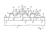
- FIG. 1 shows a cross-section of an embodiment of the pnp bipolar transistor with lateral Schottky collector.
- An n + -region 2 is formed at an upper surface of a substrate 1, which can be GaAs.
- An n-layer 3 is arranged on the n + -region 2, and a p + -layer 4 is arranged on the n-layer 3.
- the n-layer 3 and the p + -layer 4 are laterally slightly more confined than the n + -region 2 and form a mesa 16.
- the layers can be provided for additional npn transistors, which can be produced on the same substrate 1 within the same manufacturing process.
- An emitter contact layer 5, which is preferably metal, is optionally arranged on the surface of the p + -layer 4.
- a collector contact connection 11 that is formed from a metal is applied on the n-layer 3.
- the collector contact connection 11 makes a Schottky contact at the interface between the metal and the semiconductor material of the n-layer 3.
- the Schottky contact is provided as collector Schottky contact 14 of the transistor.
- the collector Schottky contact 14 comprises two separate interface areas between the n-layer 3 and the collector contact connection 11, which are shown in FIG. 1 on the left and right sides with respect to the emitter contact layer 5.
- a base contact layer 6 which is preferably metal, is arranged on an area of the upper surface of the n + -region 2 which is not covered by the n-layer 3.
- the base contact layer 6 is provided with a base contact connection 12.
- An emitter contact connection 10 is provided for the emitter and is in direct contact with the emitter contact layer 5.
- the n + -region 2 is laterally surrounded by an isolating region 7, which can be formed by an isolation implantation into the substrate, for example.
- a dielectric layer 9 can be applied on the upper surface to insulate the electrically conductive components from one another.
- the dielectric layer 9 especially covers the flanks of the mesa 16 that is formed by the n-layer 3 and the p + -layer 4.
- Space charge regions 8, which are generated under the collector Schottky contacts 14, are indicated with broken lines in FIG. 1 .
- the lateral and vertical extensions of the space charge regions 8 can deviate from those represented in FIG. 1 , depending on the operation conditions of the transistor, especially the applied electric potentials.
- FIG. 2 is a plan view onto the embodiment according to FIG. 1 not showing the dielectric layer 9.
- the position of the cross-section of FIG. 1 is indicated in FIG. 2.
- FIG. 2 shows the surface of the isolating region 7 surrounding the n + -region 2, the laterally more confined p + -layer 4 located above the n + -region 2 and covering the n-layer 3, and the marginal surface areas of the emitter contact layer 5 and the base contact layer 6.
- the arrangement of the emitter contact connection 10, the collector contact connection 11, and the base contact connection 12 as well as the areas of the emitter contact 13, the collector Schottky contact 14 and the base contact 15 are also shown in the plan view. Since the contacts 13, 14, 15 are covered by the connections 10, 11, 12, their hidden contours are represented by broken lines.
- the layout shown in FIG. 2 is only an example and can be modified and varied according to the requirements of different embodiments of the pnp transistors.
- the contact connections are preferably a metal and can be any metal that is used in a standard GaAs HBT technology.
- the collector Schottky contact 14 on opposite sides of the emitter contact 13 as shown in FIG. 2 .
- the emitter contact connection 10 and the collector contact connection 11 can be interdigitated, i. e., both connections have fingershaped extensions in comblike fashion, which are arranged in alternating sequence.
- a variety of derivatives of this layout and device structure are possible within the scope of this invention.
- the emitter contact connection 10 and/or the collector contact connection 11 can be formed in the shape of a ring or frame or have a strip-like shape. Different area ratios of the base contact 15 and the interface between the n + -region 2 and the n-layer 3 forming the base are possible.
- the layout can have more or less symmetry, and a plurality of different transistor types can be integrated in the same IC chip.
- the Schottky contact is preferred in the collector, the Schottky contact can instead be provided for the emitter.
- holes are injected into the n-layer and are captured and collected by the space charge region of the Schottky contact, thus giving a collector current. Electrons are injected in the p + -layer, thus giving a base current.
- the current level may be relatively high because of the relatively thin p + -layer, although the doping can be high in order to reduce electron injection. Holes that are injected into the n + -region recombine with electrons and give rise to extra base current. This hole injection depends on the pn junction area.
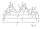
- FIG. 3 shows a cross-section of a further embodiment of the pnp bipolar transistor with lateral collector.
- a sequence comprising an n + -region 2, an n-layer 3 and a p + -layer 4 is arranged on an upper surface of the substrate 1, which can be GaAs.
- the n-layer 3 and the p + -layer 4 are laterally slightly more confined than the n + -region 2 and form a mesa 16.
- An emitter contact layer 5, which is preferably metal, is arranged on the surface of the p + -layer 4.
- the emitter contact connection 10 and the collector contact connection 11 are applied to the emitter contact layer 5 and the collector contact layer 17, respectively.
- the presence of the emitter contact layer 5 and the collector contact layer 17 is preferred, but the emitter contact connection 10 and the collector contact connection 11 can instead be applied directly to the surface of the p + -layer 4.
- the embodiment according to FIG. 1 has a better current gain.
- the performance of the embodiment of FIG. 1 depends on the control of the currents and the space charge regions.
- the space charge regions are predominantly in the n-layer 3, as shown in FIG. 1 , resulting in a significant base modulation as a function of the base-collector voltage.
- the pnp emitter needs to act as a point/line source, and the pnp collector should be constructed around the emitter to capture and collect the injected holes.
- the lateral extension of the space charge regions can be used to enhance hole capturing and collection, but attention must be paid to a possible reach-through between emitter and collector.
- FIG. 4 shows a cross-section of a further embodiment, which also comprises the sequence of an n + -region 2, an n-layer 3 and a p + -layer 4 on an upper surface of the substrate 1, which can be GaAs.
- An emitter contact connection 10 and a collector contact connection 11 are applied directly to areas of the surface of the n-layer 3 in recesses of the p + -layer 4.
- the emitter contact connection 10 forms an emitter Schottky contact 19 on the n-layer 3
- the collector contact connection 11 forms a collector Schottky contact 14 on the n-layer 3.
- FIG. 5 shows a cross-section of a further embodiment, which is comparable to the embodiment of FIG. 4 , but comprises no p + -layer 4.
- the other components of this embodiment are similar to the corresponding components of the previously described embodiments.
- the described embodiments show several ways to realize a pnp bipolar transistor in GaAs technology without having to depart from standard process steps.
- the invention therefore offers a practical way to integrate pnp bipolar transistors together with n-type devices in the same IC chip on GaAs.
Landscapes
- Bipolar Transistors (AREA)
- Bipolar Integrated Circuits (AREA)
- Electrodes Of Semiconductors (AREA)
Abstract
Description
- The field of this invention is the production of pnp bipolar transistors in gallium arsenide technology.
- Power amplifiers, especially for industrial applications, are preferably realized in GaAs technology, which provides only npn bipolar transistors but no pnp bipolar transistors. Complete integrated circuit designs are therefore not possible in GaAs technology. pnp bipolar transistors or p-type field-effect transistors can be provided on silicon chips, but a hybrid circuit concept suffers from increased current consumption and requires large device areas. In view of low cost and easy manufacturing processes, a complete integration of all the devices in GaAs technology is desired.
- Object of this invention is to present a pnp bipolar transistor that can be produced in GaAs technology and a method of producing a pnp bipolar transistor in GaAs.
- These objects and further objects are achieved by the pnp bipolar transistor with lateral collector according to
claim 1 and the method according toclaim 12. Further embodiments and variations can be derived from the dependent claims. - The invention provides a pnp bipolar transistor with a lateral collector. A base contact connection is electrically conductively connected to an n-layer. An emitter contact connection formed from a metal is electrically conductively connected to an emitter structure comprising either
- a) a Schottky contact formed by the emitter contact connection on an area of the surface of the n-layer or
- b) a p+-layer, which is arranged on an area of the surface of the n-layer, the emitter contact connection being electrically conductively connected to the p+-layer.
- A collector contact connection formed from a metal is electrically conductively connected to a collector structure, which is arranged laterally to the emitter structure with respect to the surface of the n-layer and comprises either
- a) a Schottky contact formed by the collector contact connection on an area of the surface of the n-layer or
- b) a p+-layer, which is arranged on an area of the surface of the n-layer, the collector contact connection being electrically conductively connected to the p+-layer.
- This structure has the advantage that it can be manufactured within a technology of production of GaAs devices including npn bipolar transistors.
- An embodiment of the pnp bipolar transistor comprises a substrate, which may be GaAs, and an n+-region at a surface of the substrate. The n-layer is arranged on the n+-region. The base contact connection is arranged above an area of the n+-region that is not covered by the n-layer.
- In a further embodiment of the pnp bipolar transistor, a base contact layer formed from a metal is applied to the n+-region and makes an ohmic contact with the n+-region. The base contact connection is applied to the base contact layer.
- In a further embodiment of the pnp bipolar transistor, the n-layer is part of a mesa.
- In a further embodiment of the pnp bipolar transistor, a p+-layer is arranged on the n-layer. The emitter contact connection is electrically conductively connected to the p+-layer. The collector contact connection is arranged on the surface of the n-layer and forms a collector Schottky contact at the interface between the collector contact connection and the semiconductor material of the n-layer. The portions of the p+-layer and the Schottky contact are arranged laterally to one another. The p+-layer can be provided for a base layer of additional npn bipolar transistors. The lateral arrangement of the p-type emitter and the Schottky diode provided as collector on the same surface of the n-layer uses only production steps that are compatible with standard GaAs technology, so that the production is optimally cost effective.
- In a further embodiment of the pnp bipolar transistor, the emitter contact connection forms an emitter Schottky contact on an area of the surface of the n-layer, and the collector structure comprises a p+-layer, which is arranged on an area of the surface of the n-layer.
- In a further embodiment of the pnp bipolar transistor, the emitter contact connection forms a Schottky contact on an area of the surface of the n-layer, and the collector contact connection also forms a Schottky contact on a further area of the surface of the n-layer.
- In a further embodiment of the pnp bipolar transistor, the emitter structure comprises a p+-layer, which is arranged on an area of the surface of the n-layer, and the collector structure comprises a p+-layer, which is arranged on an area of the surface of the n-layer.
- This device structure does not only provide a means of producing pnp-type bipolar transistors in the material system of gallium arsenide, but allows the production of both npn and pnp transistors integrated in the same device. The emitter-base part of the pnp transistor is arranged vertically, whereas the base-collector part of the pnp transistor is arranged laterally. Since the n-layer that serves as the base layer of the pnp transistor can also be used as a collector layer of additional npn transistors, the n-layer can be arranged on an n+-region, which is located at a surface of a semiconductor substrate of GaAs and which is provided as a subcollector for additional npn transistors to reduce the ohmic track resistance of the exterior connection to the collector layer of the npn transistors. The n-layer is arranged directly on the n+-region, which can be used in the pnp transistor to provide an electric connection of low ohmic resistance between the base contact connection and the n-layer, which serves as base layer of the pnp transistor. Further, a metal base contact layer can be arranged on the surface of the n+-region, and the base contact connection can be arranged on the base contact layer. The n-layer and the p+-layer can be structured to form a mesa, which can be electrically isolated at the sidewalls and between the contact connections on the upper side. If a base contact layer is provided, the n-layer is arranged in such a fashion that it does not cover all of the upper surface of the n+-region but leaves an area of this surface free, on which the base contact layer is placed. This metal contact layer can also be used as collector contact layer for additional npn transistors.
- A method of producing the pnp bipolar transistor with a lateral collector comprises the steps of forming an n-layer of semiconductor material and forming an emitter structure and a collector structure on the n-layer. The emitter structure and the collector structure may be produced by applying a p+-layer on the n-layer and a contact layer, formed from a metal, on the p+-layer or by applying a contact connection, formed from a metal, on the n-layer, forming a Schottky contact on the n-layer
- The method can further comprise applying a manufacturing process of an npn bipolar transistor to produce a sequence comprising an n+-region, an n-layer and a p+-layer. The n+-region can be provided to form a subcollector layer of an additional npn bipolar transistor, the n-layer to form a collector layer of the additional npn bipolar transistor and the p+-layer to form a base layer of the additional npn bipolar transistor.
- The method can further comprise forming a base contact layer on the n+-region and an emitter contact layer on the p+-layer, and applying an emitter contact connection to the emitter contact layer, a base contact connection to the base contact layer and a collector contact connection to the n-layer, the collector contact connection forming a Schottky contact on the n-layer.
- This manufacturing process can especially use a GaAs HBT technology, which was heretofore only applied to the manufacturing of npn bipolar transistors.
- After the following brief description of the drawings, a more detailed description of embodiments and examples of the pnp bipolar transistor and the method of production will be given in conjunction with the appended claims and drawings.
- FIG. 1
- shows a cross-section of an embodiment of the pnp bipolar transistor comprising a collector Schottky contact.
- FIG. 2
- shows a plan view of the embodiment according to
figure 1 . - FIG. 3
- shows a cross-section of a further embodiment of the pnp bipolar transistor having emitter and collector arranged on a p+-layer.
- FIG. 4
- shows a cross-section of a further embodiment of the pnp bipolar transistor having emitter and collector Schottky contacts.
- FIG. 5
- shows a cross-section of a further embodiment of the pnp bipolar transistor according to
FIG. 4 . -
FIG. 1 shows a cross-section of an embodiment of the pnp bipolar transistor with lateral Schottky collector. An n+-region 2 is formed at an upper surface of asubstrate 1, which can be GaAs. An n-layer 3 is arranged on the n+-region 2, and a p+-layer 4 is arranged on the n-layer 3. In this embodiment, the n-layer 3 and the p+-layer 4 are laterally slightly more confined than the n+-region 2 and form amesa 16. The layers can be provided for additional npn transistors, which can be produced on thesame substrate 1 within the same manufacturing process. Anemitter contact layer 5, which is preferably metal, is optionally arranged on the surface of the p+-layer 4. - On a surface area of the n-
layer 3 that is not covered by the p+-layer 4, acollector contact connection 11 that is formed from a metal is applied on the n-layer 3. Thecollector contact connection 11 makes a Schottky contact at the interface between the metal and the semiconductor material of the n-layer 3. The Schottky contact is provided ascollector Schottky contact 14 of the transistor. In this embodiment, thecollector Schottky contact 14 comprises two separate interface areas between the n-layer 3 and thecollector contact connection 11, which are shown inFIG. 1 on the left and right sides with respect to theemitter contact layer 5. - In order to provide an external base connection, a
base contact layer 6, which is preferably metal, is arranged on an area of the upper surface of the n+-region 2 which is not covered by the n-layer 3. Thebase contact layer 6 is provided with abase contact connection 12. - An
emitter contact connection 10 is provided for the emitter and is in direct contact with theemitter contact layer 5. The n+-region 2 is laterally surrounded by an isolatingregion 7, which can be formed by an isolation implantation into the substrate, for example. Adielectric layer 9 can be applied on the upper surface to insulate the electrically conductive components from one another. Thedielectric layer 9 especially covers the flanks of themesa 16 that is formed by the n-layer 3 and the p+-layer 4.Space charge regions 8, which are generated under thecollector Schottky contacts 14, are indicated with broken lines inFIG. 1 . The lateral and vertical extensions of thespace charge regions 8 can deviate from those represented inFIG. 1 , depending on the operation conditions of the transistor, especially the applied electric potentials. -
FIG. 2 is a plan view onto the embodiment according toFIG. 1 not showing thedielectric layer 9. The position of the cross-section ofFIG. 1 is indicated inFIG. 2. FIG. 2 shows the surface of the isolatingregion 7 surrounding the n+-region 2, the laterally more confined p+-layer 4 located above the n+-region 2 and covering the n-layer 3, and the marginal surface areas of theemitter contact layer 5 and thebase contact layer 6. The arrangement of theemitter contact connection 10, thecollector contact connection 11, and thebase contact connection 12 as well as the areas of theemitter contact 13, thecollector Schottky contact 14 and thebase contact 15 are also shown in the plan view. Since thecontacts connections FIG. 2 is only an example and can be modified and varied according to the requirements of different embodiments of the pnp transistors. The contact connections are preferably a metal and can be any metal that is used in a standard GaAs HBT technology. For good device operation it is preferred to have thecollector Schottky contact 14 on opposite sides of theemitter contact 13 as shown inFIG. 2 . In further embodiments, theemitter contact connection 10 and thecollector contact connection 11 can be interdigitated, i. e., both connections have fingershaped extensions in comblike fashion, which are arranged in alternating sequence. A variety of derivatives of this layout and device structure are possible within the scope of this invention. Theemitter contact connection 10 and/or thecollector contact connection 11 can be formed in the shape of a ring or frame or have a strip-like shape. Different area ratios of thebase contact 15 and the interface between the n+-region 2 and the n-layer 3 forming the base are possible. The layout can have more or less symmetry, and a plurality of different transistor types can be integrated in the same IC chip. Although the Schottky contact is preferred in the collector, the Schottky contact can instead be provided for the emitter. - When operating the pnp transistor, holes are injected into the n-layer and are captured and collected by the space charge region of the Schottky contact, thus giving a collector current. Electrons are injected in the p+-layer, thus giving a base current. The current level may be relatively high because of the relatively thin p+-layer, although the doping can be high in order to reduce electron injection. Holes that are injected into the n+-region recombine with electrons and give rise to extra base current. This hole injection depends on the pn junction area.
-
FIG. 3 shows a cross-section of a further embodiment of the pnp bipolar transistor with lateral collector. A sequence comprising an n+-region 2, an n-layer 3 and a p+-layer 4 is arranged on an upper surface of thesubstrate 1, which can be GaAs. As in the previous embodiment, the n-layer 3 and the p+-layer 4 are laterally slightly more confined than the n+-region 2 and form amesa 16. Anemitter contact layer 5, which is preferably metal, is arranged on the surface of the p+-layer 4. Acollector contact layer 17, which is preferably also metal, is arranged on the surface of the p+-layer 4, laterally to the emitter structure. Theemitter contact connection 10 and thecollector contact connection 11 are applied to theemitter contact layer 5 and thecollector contact layer 17, respectively. The presence of theemitter contact layer 5 and thecollector contact layer 17 is preferred, but theemitter contact connection 10 and thecollector contact connection 11 can instead be applied directly to the surface of the p+-layer 4. - Compared to a lateral pnp bipolar transistor according to
FIG. 3 , in which both emitter and collector comprise a metal layer that is applied to the p+-layer 4, the embodiment according toFIG. 1 has a better current gain. The performance of the embodiment ofFIG. 1 depends on the control of the currents and the space charge regions. The space charge regions are predominantly in the n-layer 3, as shown inFIG. 1 , resulting in a significant base modulation as a function of the base-collector voltage. To obtain a good current gain, the pnp emitter needs to act as a point/line source, and the pnp collector should be constructed around the emitter to capture and collect the injected holes. The lateral extension of the space charge regions can be used to enhance hole capturing and collection, but attention must be paid to a possible reach-through between emitter and collector. -
FIG. 4 shows a cross-section of a further embodiment, which also comprises the sequence of an n+-region 2, an n-layer 3 and a p+-layer 4 on an upper surface of thesubstrate 1, which can be GaAs. Anemitter contact connection 10 and acollector contact connection 11 are applied directly to areas of the surface of the n-layer 3 in recesses of the p+-layer 4. Theemitter contact connection 10 forms anemitter Schottky contact 19 on the n-layer 3, and thecollector contact connection 11 forms acollector Schottky contact 14 on the n-layer 3. -
FIG. 5 shows a cross-section of a further embodiment, which is comparable to the embodiment ofFIG. 4 , but comprises no p+-layer 4. The other components of this embodiment are similar to the corresponding components of the previously described embodiments. - The described embodiments show several ways to realize a pnp bipolar transistor in GaAs technology without having to depart from standard process steps. The invention therefore offers a practical way to integrate pnp bipolar transistors together with n-type devices in the same IC chip on GaAs.
-
- 1
- substrate
- 2
- n+-region
- 3
- n-layer
- 4
- p+-layer
- 5
- emitter contact layer
- 6
- base contact layer
- 7
- isolating region
- 8
- space charge region
- 9
- dielectric layer
- 10
- emitter contact connection
- 11
- collector contact connection
- 12
- base contact connection
- 13
- emitter contact
- 14
- collector Schottky contact
- 15
- base contact
- 16
- mesa
- 17
- collector contact layer
- 18
- collector contact
- 19
- emitter Schottky contact
Claims (15)
- pnp bipolar transistor with lateral collector, comprising:- an n-layer (3) having a surface,- a base contact connection (12) electrically conductively connected to the n-layer,- an emitter structure,- an emitter contact connection (10), which is a metal, electrically conductively connected to the emitter structure,- the emitter structure comprising eithera) a Schottky contact (19) formed by the emitter contact connection on an area of the surface of the n-layer orb) a p+-layer (4), which is arranged on an area of the surface of the n-layer, the emitter contact connection being electrically conductively connected to the p+-layer,- a collector structure arranged laterally to the emitter structure with respect to the surface of the n-layer,- a collector contact connection (11), which is a metal, electrically conductively connected to the collector structure,- the collector structure comprising eithera) a Schottky contact (14) formed by the collector contact connection on an area of the surface of the n-layer orb) a p+-layer (4), which is arranged on an area of the surface of the n-layer, the collector contact connection being electrically conductively connected to the p+-layer.
- The pnp bipolar transistor of claim 1, wherein the emitter structure comprises a p+-layer (4), which is arranged on an area of the surface of the n-layer (3), and
the collector contact connection (11) forms a collector Schottky contact (14) on an area of the surface of the n-layer. - The pnp bipolar transistor of claim 1, wherein the emitter contact connection (10) forms an emitter Schottky contact (19) on an area of the surface of the n-layer (3), and
the collector structure comprises a p+-layer (4), which is arranged on an area of the surface of the n-layer. - The pnp bipolar transistor of claim 1, wherein the emitter structure comprises a p+-layer (4), which is arranged on an area of the surface of the n-layer (3), and
the collector structure comprises a p+-layer (4), which is arranged on an area of the surface of the n-layer. - The pnp bipolar transistor of claim 2 or 4, further comprising:an emitter contact layer (5), which is a metal, forming an ohmic contact on the p+-layer (4), the emitter contact layer carrying the emitter contact connection (10).
- The pnp bipolar transistor of claim 3 or 4, further comprising:a collector contact layer (17), which is a metal, forming an ohmic contact on the p+-layer (4), the collectorcontact layer carrying the collector contact connection (11).
- The pnp bipolar transistor of claim 1, wherein the emitter contact connection (10) forms an emitter Schottky contact (19) on an area of the surface of the n-layer (3) and
the collector contact connection (11) forms a collector Schottky contact (14) on an area of the surface of the n-layer. - The pnp bipolar transistor of one of claims 1 to 7, further comprising:- a substrate (1) having a surface and- an n+-region (2) at the surface of the substrate, the n-layer (3) being arranged on the n+-region, and- the base contact connection (12) being arranged above an area of the n+-region that is not covered by the n-layer.
- The pnp bipolar transistor of claim 8, further comprising:a base contact layer (6), which is a metal, forming an ohmic contact on the n+-region (2), the base contact connection (12) being arranged on the base contact layer.
- The pnp bipolar transistor of one of claims 1 to 9, wherein the n-layer (3) is part of a mesa (16).
- The pnp bipolar transistor of one of claims 1 to 10, further comprising:a substrate (1), on which the pnp bipolar transistor anda vertical npn bipolar transistor are arranged, the n-layer (3) being also provided for a collector layer of the npn bipolar transistor.
- Method of producing a pnp bipolar transistor with lateral collector, comprising:- forming an n-layer (3) of semiconductor material,- forming an emitter structure on the n-layer by eithera) applying a p+-layer (4) on the n-layer, and an emitter contact layer (5) formed from a metal on the p+-layer orb) applying an emitter contact connection (10), formed from a metal, on the n-layer, forming an emitter Schottky contact (19) on the n-layer, and- forming a collector structure on the n-layer by eithera) applying a p+-layer (4) on the n-layer, and a collector contact layer (17) formed from a metal on the p+-layer orb) applying a collector contact connection (11), formed from a metal, on the n-layer, forming a collector Schottky contact (14) on the n-layer.
- The method of claim 12, further comprising:- forming an n+-region (2),- applying the n-layer (3) on the n+-region,- applying a p+-layer (4) on the n-layer,- forming an emitter contact layer (5) on the p+-layer (4),- forming a base contact layer (6) on the n+-region,- applying an emitter contact connection (10), formed from a metal, to the emitter contact layer (5),- applying a base contact connection (12), formed from a metal, to the base contact layer (6), and- applying a collector contact connection (11), formed from a metal, to the n-layer (3), the collector contact connection (11) forming a collector Schottky contact (14) on the n-layer (3).
- The method of claim 13, wherein the emitter contact layer (5) and the base contact layer (6) are formed from a metal.
- The method of claim 13 or 14, further comprising: forming an additional npn bipolar transistor, in which the n+-region (2) forms a subcollector layer, the n-layer (3) forms a collector layer, and the p+-layer (4) forms a base layer.
Priority Applications (4)
| Application Number | Priority Date | Filing Date | Title |
|---|---|---|---|
| EP08167538A EP2180517A1 (en) | 2008-10-24 | 2008-10-24 | Pnp bipolar transistor with lateral collector and method of production |
| JP2011532639A JP5336599B2 (en) | 2008-10-24 | 2009-10-22 | Bipolar transistor having n-type base and method for manufacturing the same |
| US13/124,091 US8410572B2 (en) | 2008-10-24 | 2009-10-22 | Bipolar transistor with emitter and/or collector contact structure forming a Schottky contact and method of production |
| PCT/EP2009/063921 WO2010046449A1 (en) | 2008-10-24 | 2009-10-22 | Bipolar transistor with an n-type base and method of production |
Applications Claiming Priority (1)
| Application Number | Priority Date | Filing Date | Title |
|---|---|---|---|
| EP08167538A EP2180517A1 (en) | 2008-10-24 | 2008-10-24 | Pnp bipolar transistor with lateral collector and method of production |
Publications (1)
| Publication Number | Publication Date |
|---|---|
| EP2180517A1 true EP2180517A1 (en) | 2010-04-28 |
Family
ID=40456520
Family Applications (1)
| Application Number | Title | Priority Date | Filing Date |
|---|---|---|---|
| EP08167538A Withdrawn EP2180517A1 (en) | 2008-10-24 | 2008-10-24 | Pnp bipolar transistor with lateral collector and method of production |
Country Status (4)
| Country | Link |
|---|---|
| US (1) | US8410572B2 (en) |
| EP (1) | EP2180517A1 (en) |
| JP (1) | JP5336599B2 (en) |
| WO (1) | WO2010046449A1 (en) |
Families Citing this family (4)
| Publication number | Priority date | Publication date | Assignee | Title |
|---|---|---|---|---|
| EP2187432B1 (en) * | 2008-11-13 | 2013-01-09 | Epcos AG | P-type field-effect transistor and method of production |
| JP5551790B2 (en) | 2009-12-03 | 2014-07-16 | エプコス アクチエンゲゼルシャフト | Bipolar transistor having lateral emitter and collector and manufacturing method |
| JP6068074B2 (en) * | 2012-09-20 | 2017-01-25 | 株式会社ディスコ | Method for forming gettering layer |
| US8878344B2 (en) * | 2012-10-18 | 2014-11-04 | Analog Devices, Inc. | Compound semiconductor lateral PNP bipolar transistors |
Citations (7)
| Publication number | Priority date | Publication date | Assignee | Title |
|---|---|---|---|---|
| FR2301924A1 (en) * | 1975-02-19 | 1976-09-17 | Siemens Ag | REVERSE PLANAR TRANSISTOR |
| US4127860A (en) * | 1977-04-18 | 1978-11-28 | Rca Corporation | Integrated circuit mesa bipolar device on insulating substrate incorporating Schottky barrier contact |
| US4412376A (en) * | 1979-03-30 | 1983-11-01 | Ibm Corporation | Fabrication method for vertical PNP structure with Schottky barrier diode emitter utilizing ion implantation |
| EP0443852A1 (en) * | 1990-02-22 | 1991-08-28 | Canon Kabushiki Kaisha | Lateral heterojunction bipolar transistor |
| US5438218A (en) * | 1990-06-29 | 1995-08-01 | Canon Kk | Semiconductor device with Shottky junction |
| WO2005081768A2 (en) * | 2004-02-18 | 2005-09-09 | Koucheng Wu | Schottky-barrier tunneling transistor |
| WO2007128075A2 (en) * | 2006-05-08 | 2007-11-15 | Epitactix Pty Ltd | Method and apparatus for manufacture of semiconductors and resulting structures, devices, circuits, and components |
Family Cites Families (30)
| Publication number | Priority date | Publication date | Assignee | Title |
|---|---|---|---|---|
| US4107719A (en) | 1975-02-19 | 1978-08-15 | Siemens Aktiengesellschaft | Inverse planar transistor |
| JPS5511372A (en) * | 1978-07-10 | 1980-01-26 | Mitsubishi Electric Corp | Transistor |
| JPS5632763A (en) * | 1979-08-24 | 1981-04-02 | Nec Corp | Semiconductor device |
| JPH0626242B2 (en) * | 1983-12-05 | 1994-04-06 | 富士通株式会社 | Semiconductor integrated circuit device |
| JPS6156458A (en) * | 1984-08-28 | 1986-03-22 | Matsushita Electronics Corp | semiconductor equipment |
| US4916083A (en) * | 1987-05-11 | 1990-04-10 | International Business Machines Corporation | High performance sidewall emitter transistor |
| JPH03203265A (en) * | 1989-12-28 | 1991-09-04 | Sony Corp | Semiconductor device and manufacture thereof |
| US5212102A (en) * | 1990-08-22 | 1993-05-18 | National Semiconductor Corporation | Method of making polysilicon Schottky clamped transistor and vertical fuse devices |
| US5213987A (en) * | 1991-03-28 | 1993-05-25 | Texas Instruments Incorporated | Method of integrating heterojunction bipolar transistors with PIN diodes |
| JPH06163829A (en) * | 1992-07-31 | 1994-06-10 | Texas Instr Inc <Ti> | Integrated circuit and its manufacture |
| JP3323544B2 (en) * | 1992-08-21 | 2002-09-09 | 株式会社日立製作所 | Semiconductor device |
| JPH0738079A (en) * | 1993-07-26 | 1995-02-07 | Fujitsu Ltd | Hot carrier semiconductor device |
| US5535231A (en) * | 1994-11-08 | 1996-07-09 | Samsung Electronics Co., Ltd. | Optoelectronic circuit including heterojunction bipolar transistor laser and photodetector |
| US5449627A (en) * | 1994-12-14 | 1995-09-12 | United Microelectronics Corporation | Lateral bipolar transistor and FET compatible process for making it |
| JPH1065015A (en) * | 1996-08-19 | 1998-03-06 | Sony Corp | Semiconductor device and manufacturing method thereof |
| SE515158C2 (en) * | 1999-02-10 | 2001-06-18 | Ericsson Telefon Ab L M | Semiconductor device with ground connection via a non-through plug |
| US6407617B1 (en) * | 1999-11-19 | 2002-06-18 | Matsushita Electric Industrial Co., Ltd. | Bias circuit and method of fabricating semiconductor device |
| JP2001217317A (en) * | 2000-02-07 | 2001-08-10 | Sony Corp | Semiconductor device and method of manufacturing the same |
| JP4065104B2 (en) * | 2000-12-25 | 2008-03-19 | 三洋電機株式会社 | Semiconductor integrated circuit device and manufacturing method thereof |
| US6406965B1 (en) * | 2001-04-19 | 2002-06-18 | Trw Inc. | Method of fabricating HBT devices |
| JP2003243527A (en) * | 2002-02-15 | 2003-08-29 | Hitachi Ltd | Method for manufacturing semiconductor device |
| JP3976601B2 (en) * | 2002-03-28 | 2007-09-19 | 株式会社ルネサステクノロジ | Manufacturing method of semiconductor device |
| US6759731B2 (en) * | 2002-06-05 | 2004-07-06 | United Microelectronics Corp. | Bipolar junction transistor and fabricating method |
| US6888710B2 (en) * | 2003-01-03 | 2005-05-03 | Micrel, Incorporated | Insulated gate bipolar transistor and electrostatic discharge cell protection utilizing insulated gate bipolar transistors |
| JP2005005446A (en) * | 2003-06-11 | 2005-01-06 | Renesas Technology Corp | Semiconductor device and manufacturing method thereof |
| US7049201B2 (en) * | 2003-11-06 | 2006-05-23 | Chartered Semionductor Manufacturing Ltd. | Method and apparatus for a heterojunction bipolar transistor using self-aligned epitaxy |
| JP2007243140A (en) * | 2006-02-09 | 2007-09-20 | Renesas Technology Corp | Semiconductor device, electronic device, and manufacturing method of semiconductor device |
| ITTO20060525A1 (en) * | 2006-07-18 | 2008-01-19 | St Microelectronics Srl | INTEGRATED BIPOLAR DEVICE OF VERTICAL TYPE AND ITS PROCEDURE FOR ITS MANUFACTURE |
| US7868414B2 (en) * | 2007-03-28 | 2011-01-11 | Advanced Analogic Technologies, Inc. | Isolated bipolar transistor |
| JP2009021313A (en) * | 2007-07-11 | 2009-01-29 | Hitachi Ltd | Semiconductor device |
-
2008
- 2008-10-24 EP EP08167538A patent/EP2180517A1/en not_active Withdrawn
-
2009
- 2009-10-22 US US13/124,091 patent/US8410572B2/en not_active Expired - Fee Related
- 2009-10-22 JP JP2011532639A patent/JP5336599B2/en not_active Expired - Fee Related
- 2009-10-22 WO PCT/EP2009/063921 patent/WO2010046449A1/en not_active Ceased
Patent Citations (7)
| Publication number | Priority date | Publication date | Assignee | Title |
|---|---|---|---|---|
| FR2301924A1 (en) * | 1975-02-19 | 1976-09-17 | Siemens Ag | REVERSE PLANAR TRANSISTOR |
| US4127860A (en) * | 1977-04-18 | 1978-11-28 | Rca Corporation | Integrated circuit mesa bipolar device on insulating substrate incorporating Schottky barrier contact |
| US4412376A (en) * | 1979-03-30 | 1983-11-01 | Ibm Corporation | Fabrication method for vertical PNP structure with Schottky barrier diode emitter utilizing ion implantation |
| EP0443852A1 (en) * | 1990-02-22 | 1991-08-28 | Canon Kabushiki Kaisha | Lateral heterojunction bipolar transistor |
| US5438218A (en) * | 1990-06-29 | 1995-08-01 | Canon Kk | Semiconductor device with Shottky junction |
| WO2005081768A2 (en) * | 2004-02-18 | 2005-09-09 | Koucheng Wu | Schottky-barrier tunneling transistor |
| WO2007128075A2 (en) * | 2006-05-08 | 2007-11-15 | Epitactix Pty Ltd | Method and apparatus for manufacture of semiconductors and resulting structures, devices, circuits, and components |
Non-Patent Citations (5)
| Title |
|---|
| EMEIS N ET AL: "FABRICATION OF WIDEGAP-EMITTER SCHOTTKY-COLLECTOR TRANSISTOR USING GalnAs/InP", ELECTRONICS LETTERS,, vol. 21, no. 3, 1 January 1985 (1985-01-01), pages 85, XP001291780 * |
| KUMAR M J ET AL: "A New High Breakdown Voltage Lateral Schottky Collector Bipolar Transistor on SOI: Design and Analysis", IEEE TRANSACTIONS ON ELECTRON DEVICES, IEEE SERVICE CENTER, PISACATAWAY, NJ, US, vol. 52, no. 11, 1 November 2005 (2005-11-01), pages 2496 - 2501, XP011141565, ISSN: 0018-9383, DOI: 10.1109/TED.2005.857171 * |
| KUMAR M J ET AL: "A new lateral PNM Schottky collector bipolar transistor (SCBT) on SOI for nonsaturating VLSI logic design", IEEE TRANSACTIONS ON ELECTRON DEVICES, 1 June 2002 (2002-06-01), pages 1070 - 1072, XP055665253, Retrieved from the Internet <URL:https://ieeexplore.ieee.org/ielx5/16/21668/01003748.pdf?tp=&arnumber=1003748&isnumber=21668&ref=aHR0cHM6Ly9pZWVleHBsb3JlLmllZWUub3JnL2RvY3VtZW50LzEwMDM3NDg=> DOI: 10.1109/TED.2002.1003748 * |
| MAY ET AL: "The Schottky-barrier-collector transistor", SOLID STATE ELECTRONICS, ELSEVIER SCIENCE PUBLISHERS, BARKING, GB, vol. 11, no. 6, 1 June 1968 (1968-06-01), pages 613 - 619, XP024634111, ISSN: 0038-1101, DOI: 10.1016/0038-1101(68)90014-2 * |
| S. AKBAR ET AL: "Schottky-collector vertical PNM bipolar transistor", ELECTRONICS LETTERS, vol. 28, no. 1, 2 January 1992 (1992-01-02), GB, pages 86 - 87, XP055665417, ISSN: 0013-5194, DOI: 10.1049/el:19920053 * |
Also Published As
| Publication number | Publication date |
|---|---|
| JP5336599B2 (en) | 2013-11-06 |
| US20110248375A1 (en) | 2011-10-13 |
| WO2010046449A1 (en) | 2010-04-29 |
| US8410572B2 (en) | 2013-04-02 |
| JP2012506630A (en) | 2012-03-15 |
Similar Documents
| Publication | Publication Date | Title |
|---|---|---|
| KR100208632B1 (en) | Semiconductor integrated circuit and manufacturing method thereof | |
| US20040048428A1 (en) | Semiconductor device and method of manufacturing the same | |
| US9691874B2 (en) | Manufacturing method of semiconductor structure | |
| US8410572B2 (en) | Bipolar transistor with emitter and/or collector contact structure forming a Schottky contact and method of production | |
| TWI677073B (en) | Bipolar junction transistor layout structure | |
| US5399899A (en) | Bipolar epitaxial cascode with low-level base connection | |
| CN115732553A (en) | IGBT device and preparation method thereof | |
| US7755168B2 (en) | Semiconductor device provided with floating electrode | |
| US8563387B2 (en) | Transistor and method of manufacturing a transistor | |
| US11183586B2 (en) | Cascode transistor device | |
| JP2004128142A (en) | Semiconductor device and manufacturing method thereof | |
| EP0605920B1 (en) | Cascode circuit structure with epitaxial bipolar transistors comprising a low-level base connection | |
| US7352051B2 (en) | Cascode, cascode circuit and method for vertical integration of two bipolar transistors into a cascode arrangement | |
| US8581339B2 (en) | Structure of NPN-BJT for improving punch through between collector and emitter | |
| JPH055373B2 (en) | ||
| CN202940239U (en) | Multi-transistor structure and semiconductor device with same | |
| US20260033385A1 (en) | Humidity sensor and integrated circuit including same | |
| KR20120068069A (en) | Semiconductor device and manufacturing method used the same | |
| JP2001203358A (en) | Dielectric separated type semiconductor device | |
| EP1061572A1 (en) | Intergrated stucture for radio frequency applications | |
| JP2002299465A (en) | Semiconductor device | |
| US8319315B2 (en) | Bipolar junction transistor devices | |
| JP2000183076A (en) | Semiconductor device and manufacturing method thereof | |
| CN102931225A (en) | A kind of bipolar junction transistor and its manufacturing method | |
| JP2001230260A (en) | Semiconductor device and method of manufacturing semiconductor device |
Legal Events
| Date | Code | Title | Description |
|---|---|---|---|
| PUAI | Public reference made under article 153(3) epc to a published international application that has entered the european phase |
Free format text: ORIGINAL CODE: 0009012 |
|
| AK | Designated contracting states |
Kind code of ref document: A1 Designated state(s): AT BE BG CH CY CZ DE DK EE ES FI FR GB GR HR HU IE IS IT LI LT LU LV MC MT NL NO PL PT RO SE SI SK TR |
|
| AX | Request for extension of the european patent |
Extension state: AL BA MK RS |
|
| 17P | Request for examination filed |
Effective date: 20100929 |
|
| AKX | Designation fees paid |
Designated state(s): DE |
|
| 17Q | First examination report despatched |
Effective date: 20150727 |
|
| RAP1 | Party data changed (applicant data changed or rights of an application transferred) |
Owner name: SNAPTRACK, INC. |
|
| STAA | Information on the status of an ep patent application or granted ep patent |
Free format text: STATUS: EXAMINATION IS IN PROGRESS |
|
| GRAP | Despatch of communication of intention to grant a patent |
Free format text: ORIGINAL CODE: EPIDOSNIGR1 |
|
| STAA | Information on the status of an ep patent application or granted ep patent |
Free format text: STATUS: GRANT OF PATENT IS INTENDED |
|
| INTG | Intention to grant announced |
Effective date: 20200409 |
|
| GRAJ | Information related to disapproval of communication of intention to grant by the applicant or resumption of examination proceedings by the epo deleted |
Free format text: ORIGINAL CODE: EPIDOSDIGR1 |
|
| STAA | Information on the status of an ep patent application or granted ep patent |
Free format text: STATUS: EXAMINATION IS IN PROGRESS |
|
| INTC | Intention to grant announced (deleted) | ||
| GRAP | Despatch of communication of intention to grant a patent |
Free format text: ORIGINAL CODE: EPIDOSNIGR1 |
|
| STAA | Information on the status of an ep patent application or granted ep patent |
Free format text: STATUS: GRANT OF PATENT IS INTENDED |
|
| INTG | Intention to grant announced |
Effective date: 20201201 |
|
| STAA | Information on the status of an ep patent application or granted ep patent |
Free format text: STATUS: THE APPLICATION IS DEEMED TO BE WITHDRAWN |
|
| 18D | Application deemed to be withdrawn |
Effective date: 20210413 |