EP2169792B1 - Semiconductor laser and method for manufacturing the same - Google Patents
Semiconductor laser and method for manufacturing the same Download PDFInfo
- Publication number
- EP2169792B1 EP2169792B1 EP08765318.4A EP08765318A EP2169792B1 EP 2169792 B1 EP2169792 B1 EP 2169792B1 EP 08765318 A EP08765318 A EP 08765318A EP 2169792 B1 EP2169792 B1 EP 2169792B1
- Authority
- EP
- European Patent Office
- Prior art keywords
- layer
- ridge portion
- type
- semiconductor laser
- wtop
- Prior art date
- Legal status (The legal status is an assumption and is not a legal conclusion. Google has not performed a legal analysis and makes no representation as to the accuracy of the status listed.)
- Not-in-force
Links
Images


Classifications
-
- B—PERFORMING OPERATIONS; TRANSPORTING
- B82—NANOTECHNOLOGY
- B82Y—SPECIFIC USES OR APPLICATIONS OF NANOSTRUCTURES; MEASUREMENT OR ANALYSIS OF NANOSTRUCTURES; MANUFACTURE OR TREATMENT OF NANOSTRUCTURES
- B82Y20/00—Nanooptics, e.g. quantum optics or photonic crystals
-
- H—ELECTRICITY
- H01—ELECTRIC ELEMENTS
- H01S—DEVICES USING THE PROCESS OF LIGHT AMPLIFICATION BY STIMULATED EMISSION OF RADIATION [LASER] TO AMPLIFY OR GENERATE LIGHT; DEVICES USING STIMULATED EMISSION OF ELECTROMAGNETIC RADIATION IN WAVE RANGES OTHER THAN OPTICAL
- H01S5/00—Semiconductor lasers
- H01S5/20—Structure or shape of the semiconductor body to guide the optical wave ; Confining structures perpendicular to the optical axis, e.g. index or gain guiding, stripe geometry, broad area lasers, gain tailoring, transverse or lateral reflectors, special cladding structures, MQW barrier reflection layers
- H01S5/22—Structure or shape of the semiconductor body to guide the optical wave ; Confining structures perpendicular to the optical axis, e.g. index or gain guiding, stripe geometry, broad area lasers, gain tailoring, transverse or lateral reflectors, special cladding structures, MQW barrier reflection layers having a ridge or stripe structure
- H01S5/223—Buried stripe structure
- H01S5/2231—Buried stripe structure with inner confining structure only between the active layer and the upper electrode
-
- H—ELECTRICITY
- H01—ELECTRIC ELEMENTS
- H01S—DEVICES USING THE PROCESS OF LIGHT AMPLIFICATION BY STIMULATED EMISSION OF RADIATION [LASER] TO AMPLIFY OR GENERATE LIGHT; DEVICES USING STIMULATED EMISSION OF ELECTROMAGNETIC RADIATION IN WAVE RANGES OTHER THAN OPTICAL
- H01S5/00—Semiconductor lasers
- H01S5/06—Arrangements for controlling the laser output parameters, e.g. by operating on the active medium
- H01S5/065—Mode locking; Mode suppression; Mode selection ; Self pulsating
- H01S5/0651—Mode control
- H01S5/0653—Mode suppression, e.g. specific multimode
- H01S5/0655—Single transverse or lateral mode emission
-
- H—ELECTRICITY
- H01—ELECTRIC ELEMENTS
- H01S—DEVICES USING THE PROCESS OF LIGHT AMPLIFICATION BY STIMULATED EMISSION OF RADIATION [LASER] TO AMPLIFY OR GENERATE LIGHT; DEVICES USING STIMULATED EMISSION OF ELECTROMAGNETIC RADIATION IN WAVE RANGES OTHER THAN OPTICAL
- H01S5/00—Semiconductor lasers
- H01S5/20—Structure or shape of the semiconductor body to guide the optical wave ; Confining structures perpendicular to the optical axis, e.g. index or gain guiding, stripe geometry, broad area lasers, gain tailoring, transverse or lateral reflectors, special cladding structures, MQW barrier reflection layers
- H01S5/2054—Methods of obtaining the confinement
- H01S5/2081—Methods of obtaining the confinement using special etching techniques
- H01S5/2086—Methods of obtaining the confinement using special etching techniques lateral etch control, e.g. mask induced
-
- H—ELECTRICITY
- H01—ELECTRIC ELEMENTS
- H01S—DEVICES USING THE PROCESS OF LIGHT AMPLIFICATION BY STIMULATED EMISSION OF RADIATION [LASER] TO AMPLIFY OR GENERATE LIGHT; DEVICES USING STIMULATED EMISSION OF ELECTROMAGNETIC RADIATION IN WAVE RANGES OTHER THAN OPTICAL
- H01S5/00—Semiconductor lasers
- H01S5/30—Structure or shape of the active region; Materials used for the active region
- H01S5/34—Structure or shape of the active region; Materials used for the active region comprising quantum well or superlattice structures, e.g. single quantum well [SQW] lasers, multiple quantum well [MQW] lasers or graded index separate confinement heterostructure [GRINSCH] lasers
- H01S5/341—Structures having reduced dimensionality, e.g. quantum wires
- H01S5/3412—Structures having reduced dimensionality, e.g. quantum wires quantum box or quantum dash
Definitions
- the present invention relates to a semiconductor laser and a method for manufacturing the same, and more particularly to a semiconductor laser having a plurality of quantum dots as an active layer and a method for manufacturing the same.
- Patent Document 1 discloses a method for forming quantum dots.
- Patent Document 2 discloses a semiconductor laser in which at least part of an active layer including a plurality of quantum dots is formed of p-type semiconductor in order to achieve high-speed modulation and high reliability.
- a p-type clad layer 2 and a quantum dot active layer 3 are stacked on a p-type GaAs substrate 1.
- An n-type clad layer 4 having a convex shape (ridge portion) is provided on the quantum dot active layer 3.
- the n-type clad layer 4 is formed only at a central portion of the quantum dot active layer 3.
- an area of p-n junction formed by the quantum dot active layer 3 and the n-type clad layer 4 can be reduced. Therefore, the parasitic capacitance can be reduced, so that high-speed modulation can be achieved.
- JPH05 304336 discloses a buried mesa semiconductor laser device with: a n-type lower clad; a quantum-well active layer; a p-type upper clad; an electrode on the upper clad; wherein the upper clad layer comprises first AlGaAs layer with higher Al-composition and second AlGaAs layer with lower Al-composition, both formed by wet etching.
- the convex shape (ridge portion) of Patent Document 2 is formed by wet etching.
- Figs. 1A to 2B show examples of cases where a ridge portion is formed by wet etching, and are cross-sectional views taken perpendicular to a direction of light propagation.
- a p-type clad layer 12 as a lower clad layer, a quantum dot active layer 14, and an n-type clad layer 18 as an upper clad layer are formed on a p-type substrate 10.
- the n-type clad layer 18 has a ridge portion 30.
- An n-electrode 22 is provided on an upper surface of the ridge portion 30, and a p-electrode 24 is provided below the substrate 10.
- the ridge portion 30 of the n-type clad layer 18 is formed by wet etching, it has a trapezoidal shape. Specifically, as shown in Fig. 1A , the width Wbot of a bottom of the ridge portion 30 is greater than the width Wtop of a top of the ridge portion 30.
- a guided mode of the fundamental mode M0 is generated in the quantum dot active layer 14 located below the ridge portion 30 as shown in Fig. 1A .
- a guided mode of the first higher mode M1 is also formed in the quantum dot active layer 14 located below the ridge portion 30.
- the quantum dot active layer 14 located below the ridge portion 30 and its vicinity are a waveguide region of oscillated light, light having a wavelength of the first higher mode M1 is mixed into the oscillated light if the first higher mode M1 is formed in the quantum dot active layer 14 located below the ridge portion 30.
- the reason why the first higher mode M1 is thus formed below the ridge portion 30 is because the width Wbot is large.
- Figs. 2A and 2B show a case where the width Wbot of the bottom of the ridge portion 30 is reduced.
- the fundamental mode M0 is formed in the quantum dot active layer 14 located below the ridge portion 30.
- the first higher mode M1 is formed in the quantum dot active layer 14 at both sides of a portion located below the ridge portion 30. Therefore, the first higher mode M1 can be prevented from being mixed into oscillated light.
- the width Wbot is reduced, the width Wtop of the top of the ridge portion 30 is also reduced.
- the n-electrode 22 is formed on the upper surface of the ridge portion 30. If the width Wtop is reduced, a contact resistance between the n-type clad layer 18 and the n-electrode 22 is increased so as to inhibit high-speed modulation.
- the present invention has been made in view of the above problems. It is, therefore, an object of the present invention to prevent higher modes from being mixed into oscillated light in a quantum dot semiconductor laser and reduce a contact resistance between an upper clad layer and an electrode.
- the present invention provides a semiconductor laser as defined in claim 1. According to the present invention, higher modes can be prevented from being mixed into oscillated light, and a contact resistance between the upper clad layer and the electrode can be reduced.
- the upper clad layer includes a first layer and a second layer provided on the first layer, and the first layer has a minimum width of the ridge portion.
- the semiconductor laser are configured such that the first layer and the second layer comprise an AlGaAs layer and that an Al compositional ratio of the first layer is higher than that of the second layer.
- the semiconductor laser is configured to have a third layer provided on the second layer, the third layer having a concentration of the second conductive type of carriers that is higher than those of the first layer and the second layer.
- the semiconductor laser may be configured such that the plurality of quantum dots is formed of InGaAs or InAs and that the active layer includes a barrier layer of AlGaAs or GaAs that surrounds the plurality of quantum dots.
- the semiconductor laser may be configured such that the first conductive type is p-type, that the second conductive type is n-type, and that the barrier layer has a p-type layer.
- the semiconductor laser may be configured to have an undoped layer between the active layer and the upper clad layer.
- the present invention provides a method for manufacturing a semiconductor laser, the method being as defined in claim 6.
- the second layer is dry-etched, a side surface of the upper clad layer can be made steep. Therefore, higher modes are prevented from being mixed into oscillated light, and a contact resistance between the upper clad layer and the electrode can be reduced. Furthermore, since the first layer is wet-etched, the active layer is prevented from being over-etched.
- the method is configured such that the first layer and the second layer comprise an AlGaAs layer and that an Al compositional ratio of the first layer is higher than that of the second layer.
- an etching rate of wet etching of the first layer is made higher than that of the second layer.
- the side surface of the ridge portion are made steeper.
- the method is configured such that the minimum width of the ridge portion located in the first AlGaAs layer is smaller than the width of the top of the ridge portion.
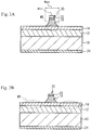
- a ridge portion 30 has a cross-section having a rectangular shape. Specifically, the width Wtop of a top of the ridge portion 30 is almost the same as the width Wbot of a bottom of the ridge portion 30. Other structures are the same as those of Figs. 1A to 2B .
- the fundamental mode M0 is formed in a quantum dot active layer 14 located below the ridge portion 30.
- the first higher mode M1 is formed in the quantum dot active layer 14 at both sides of a portion located below the ridge portion 30.
- the width Wtop can be increased as compared to Fig. 2A . Therefore, a contact resistance between an n-type clad layer 18 and an n-electrode 22 can be reduced.
- the width Wtop of the top of the ridge portion 30 is set to be equal to or greater than the width Wbot of the bottom of the ridge portion 30. This configuration can suppress mixture of higher modes and enables high-speed modulation.
- a first conductive type is p-type
- a second conductive type opposite to the first conductive type is n-type
- the first conductive type may be n-type
- the second conductive type may be p-type
- the semiconductor substrate may be of n-type
- the lower clad layer may be of n-type
- the upper clad layer may be of p-type.
- Figs. 4A to 4D are cross-sectional views showing a process of manufacturing a semiconductor laser according to Example 1.
- a p-type clad layer 12 lower clad layer
- a quantum dot active layer 14 having a plurality of quantum dots and an n-type clad layer 18 (upper clad layer) are sequentially stacked and formed on a p-type semiconductor substrate 10 by using, for example, an MBE (Molecular Beam Epitaxy) method.
- the n-type clad layer 18 includes a first layer 81 and a second layer 82.
- a photoresist 32 is formed on the n-type clad layer 18. While the photoresist 32 is used as a mask, the n-type clad layer 18 is subjected to anisotropic etching that reaches the first layer 81 by a dry etching method. At that time, a side surface of the n-type clad layer 18 becomes almost perpendicular.
- the first layer 81 of the n-type clad layer 18 is etched by using wet etching. At that time, materials of the respective layers and an etchant are selected such that an etching rate of the first layer 81 is higher than those of the quantum dot active layer 14 and the second layer 82. Thus, the first layer 81 and the side surface are etched, so that a ridge portion 30 is formed. In this manner, the n-type clad layer 18 having the ridge portion 30 is formed on the quantum dot active layer 14. The etching rate of the first layer 81 is so high that a constriction 85 of the ridge portion 30 is formed on the first layer 81. The photoresist 32 is then removed.
- an n-electrode 22 is formed above the n-type clad layer 18, and a p-electrode 24 is formed below the p-type substrate 10.
- a semiconductor laser according to Example 1 is completed.
- the n-type clad layer 18 is formed into an isolated ridge portion 30 on the quantum dot active layer 14 by dry-etching the second layer 82 as shown in Fig. 4B and wet-etching the first layer 81 as shown in Fig. 4C .
- the second layer 82 is dry-etched, the side surface of the n-type clad layer 18 can be made steep. Therefore, higher modes are prevented from being mixed into oscillated light, and a contact resistance between the n-type clad layer 18 and the n-electrode 22 can be reduced.
- the first layer 81 is wet-etched, the quantum dot active layer 14 is prevented from being over-etched.
- the n-type clad layer 18 is formed of, for example, an AlGaAs layer, and the Al compositional ratio of the first layer 81 is set to be higher than that of the second layer 82.
- An AlGaAs layer has a higher rate of wet etching as it has a higher Al compositional ratio.
- the first layer 81 is wet-etched with a hydrofluoric acid solution, so that the first layer 81 can be etched selectively with respect to the second layer 82.
- the first layer 81 can have a minimum width of the ridge portion 30.
- an etching rate of wet etching of an AlGaAs layer drastically increases if an Al compositional ratio exceeds 0.4. Therefore, it is preferable to adjust an Al compositional ratio of the first layer 81 to be at least 0.4 and to adjust an Al compositional ratio of the second layer 82 to be lower than 0.4. Moreover, it is preferable to adjust the film thickness of the first layer 81 to be equal to or smaller than 0.3 ⁇ m in order to reduce a resistance between the quantum dot active layer 14 and the second layer 82.
- Example 1 Guided modes were simulated in Example 1 and an example (Comparative Example 1) in which the ridge portion 30 was formed by wet etching as shown in Figs. 1A and 2A .
- Fig. 5 is a diagram showing a cross-section of a semiconductor laser used for the simulation of Comparative Example 1, not falling under the present invention.
- Fig. 6 is a diagram showing a cross-section of a semiconductor laser used for the simulation of Example 1, according to the invention.
- An n-type clad layer 18 was formed by a first layer 81 of Al 0.45 Ga 0.55 As having a film thickness of 200 nm and a second layer 82 of Al 0.35 Ga 0.65 As having a film thickness of 1400 nm. A side surface of the second layer 82 became almost perpendicular, and a constriction 85 was formed on the first layer 81.
- Figs. 7A and 7B are diagrams showing simulated structures of Comparative Example 1 and Example 1, respectively.
- Optical confinement factors ⁇ 0 and ⁇ 1 of the fundamental mode M0 and the first higher mode M1 were respectively defined by values into which the intensity of light in regions R (the quantum dot active layer 14 located below the ridge portion 30) of Figs. 7A and 7B was normalized by the all-optical intensity of each mode.
- Fig. 8 is the simulation results showing the optical confinement factors ⁇ 0 and ⁇ 1 of the semiconductor lasers according to Comparative Example 1 and Example 1 with respect to Wtop.
- the open circles represent the simulation result of Comparative Example 1, whereas the filled circles represent the simulation result of Example 1.
- the dashed lines and the solid lines are approximation lines connecting the simulation results of Comparative Example 1 and Example 1, respectively.
- the optical confinement factor ⁇ 1 of the first higher mode M1 ranged from 0.2 to 0.4.
- the optical confinement factor ⁇ 1 was not higher than 0.2.
- ⁇ 1 was almost zero when Wtop was equal to or less than 2.0 ⁇ m.
- ⁇ 1 was almost zero when Wtop was equal to or less than 1.8 ⁇ m.
- Example 1 ⁇ 1 could be made almost zero by optimizing Wtop. Furthermore, the optical confinement factor ⁇ 0 of the fundamental mode M0 in Example 1 was also higher than that in Comparative Example 1. Accordingly, in Example 1, higher modes in the region R could be suppressed, and the intensity of the fundamental mode in the region R could be increased.
- the width Wtop of the top of the ridge portion 30 is set to be equal to or greater than the width Wbot of the bottom of the ridge portion 30, higher modes can be prevented from being mixed into oscillated light. Therefore, the intensity of the fundamental mode in the region R can be increased. Furthermore, since Wtop can be increased in a state in which higher modes are prevented from being mixed into oscillated light, a contact resistance between the n-type clad layer 18 and the n-electrode 22 can be reduced.
- Example 2 is an example that does not fall under the present invention and that can suppress higher modes and increase the intensity of the fundamental mode in the region R, as with Example 1, in a case where the width Wtop of the top of the ridge portion 30 was smaller than the width Wbot of the bottom of the ridge portion 30.
- Fig. 9 is a graph showing the simulation results of the optical confinement factor ⁇ 0 of the fundamental mode M0, the optical confinement factor ⁇ 1 of the first higher mode M1, and ⁇ 1/ ⁇ 0 when a value of W1 - Wtop was varied in the semiconductor laser of Comparative Example 1 shown in Fig. 5 .
- Wtop 1.5 ⁇ m
- W2 - Wtop (3/4)(W1 - Wtop).
- the filled circles represent the simulation results, the solid lines are approximation lines connecting the simulation results.
- the optical confinement factor ⁇ 1 of the first higher mode M1 can be lower than ⁇ 1 of the case where W1 > Wtop + 0.6 ⁇ m. Therefore, higher modes in the region R can be suppressed, and the intensity of the fundamental mode in the region R can be increased. Furthermore, when W1 ⁇ Wtop + 0.2 ⁇ m, ⁇ 1 can be made almost zero.
- Fig. 10 is a graph showing the optical confinement factor ⁇ 0 of the fundamental mode M0 and the optical confinement factor ⁇ 1 of the first higher mode M1 when Wtop was varied.
- the solid lines and the dashed lines are lines connecting the simulation results.
- Wtop is preferably set to be equal to or less than 2.0 ⁇ m, more preferably equal to or less than 1.8 ⁇ m, and still more preferably equal to or less than 1.6 ⁇ m.
- Example 3 is an example of production of a semiconductor laser that does not fall under the present invention.
- Fig. 11 is a cross-sectional perspective view of Example 3.
- Table 1 shows the material, the film thickness, and the doping concentration of each layer.
- Layer name Material Film thickness (nm) Doping concentration (/cm 3 ) Contact layer n-GaAs 600 5 ⁇ 10 18 N-type clad layer n-Al 0.35 Ga 0.65 As 860 1 ⁇ 10 18 n-Al 0.45 Ga 0.55 As 200 5 ⁇ 10 17 Spacer layer GaAs 50 Undoped Active layer - - - Spacer layer GaAs 33 Undoped P-type clad layer p-Al 0.35 Ga 0.65 As 500 5 ⁇ 10 17 p-Al 0.35 Ga 0.65 As 900 2 ⁇ 10 18 Buffer layer p-GaAs 500 7 ⁇ 10 18 Substrate p-GaAs - - -
- the n-type clad layer 18 and the contact layer 19 formed a ridge portion 30.
- Recessed portions 35 that reached the spacer layer 16 were formed on both sides of the ridge portion 30.
- a silicon oxide film was formed as a protective film 28 on the contact layer 19 and surfaces of the recessed portions 35.
- An n-electrode 22 was formed on the contact layer 19 of the ridge portion 30.
- a pad 26 connecting to the n-electrode 22 via an interconnection 25 was formed.
- a p-electrode 24 was formed on a lower surface of the substrate 10.
- Fig. 12 is a diagram showing a dot layer 40 as one layer of the quantum dot active layer.
- the quantum dots 41 are formed of InAs.
- An InGaAs layer 42 having a film thickness of about 5 nm is formed between the quantum dots 41.
- An undoped GaAs layer 43 having a film thickness of about 14 nm is formed so as to cover the quantum dots 41 and the InGaAs layer 42.
- a p-type GaAs layer 44 having a film thickness of about 10 nm and an undoped GaAs layer 45 having a film thickness of 9 nm are formed on the undoped GaAs layer 43.
- the undoped GaAs layer 43, the p-type GaAs layer 44, and the undoped GaAs layer 45 form a barrier layer 46.
- Table 2 shows the material, the film thickness, and the doping concentration of each layer in the quantum dot active layer 14.
- Layer name Material Film thickness (nm) Doping concentration (/cm 3 ) Undoped GaAs layer GaAs 9 Undoped P-type GaAs layer p-GaAs 10 5 ⁇ 10 17 Undoped GaAs layer GaAs 14 Undoped InGaAs layer In 0.15 Ga 0.85 As 5 Undoped
- Fig. 13 is a graph showing the maximum modulation band of a semiconductor laser with respect to the number of dot layers.
- the filled circles of Fig. 13 represent maximum modulation bands of semiconductor lasers produced as a trial in which the number of the dot layers 40 was 10 layers and 12 layers.
- the solid line represents the simulation results.
- the maximum modulation band increased as the number of the dot layers 40 increased.
- the maximum modulation band could be increased to at least 10 GHz by providing 12 or more dot layers 40 as shown in Fig. 13 .
- the contact layer 19 (third layer) was provided on the second layer 82.
- the n-type carrier concentration of the contact layer 19 was higher than those of the first layer 81 and the second layer 82.
- a contact resistance between the n-electrode 22 and the n-type clad layer 18 could be reduced.
- a plurality of quantum dots 41 is formed of InAs.
- the quantum dots 41 should only have a band gap smaller than the barrier layer 46.
- the barrier layer 46 surrounding a plurality of quantum dots 41 in the quantum dot active layer 14 is formed of GaAs and InGaAs.
- the barrier layer 46 may be formed of AlGaAs.
- the n-type clad layer 18 has a ridge structure in order to reduce an area of p-n junction in many cases where the barrier layer 46 includes a p-type layer. At that time, it is effective to apply the present invention in order to suppress higher modes. It is preferable to form the p-type layer within 30 nm from the quantum dots 41.
- the undoped spacer layer 16 between the quantum dot active layer 14 and the n-type clad layer 18 as shown in Fig. 11 .
- the quantum dot active layer 14 can be prevented from being over-etched when the ridge portion 30 is formed.
- the spacer layer 16 it is preferable for the spacer layer 16 to have a film thickness of at least 50 nm in order to protect the quantum dot active layer 14.
- the area of the pad 26 is preferably equal to or smaller than 40000 ⁇ m 2 .
Description
- The present invention relates to a semiconductor laser and a method for manufacturing the same, and more particularly to a semiconductor laser having a plurality of quantum dots as an active layer and a method for manufacturing the same.
- Semiconductor lasers used for an active layer having quantum dots have been developed in recent years.
Patent Document 1 discloses a method for forming quantum dots.Patent Document 2 discloses a semiconductor laser in which at least part of an active layer including a plurality of quantum dots is formed of p-type semiconductor in order to achieve high-speed modulation and high reliability. - Referring to
Fig. 1E ofPatent Document 2, a p-type clad layer 2 and a quantum dot active layer 3 are stacked on a p-type GaAs substrate 1. An n-type clad layer 4 having a convex shape (ridge portion) is provided on the quantum dot active layer 3. The n-type clad layer 4 is formed only at a central portion of the quantum dot active layer 3. Thus, an area of p-n junction formed by the quantum dot active layer 3 and the n-type clad layer 4 can be reduced. Therefore, the parasitic capacitance can be reduced, so that high-speed modulation can be achieved. - Patent Document 1: Japanese patent No.
3468866 - Patent Document 2: Japanese laid-open patent publication No.
2006-286902 -
JPH05 304336 - As described at paragraph 0025 of
Patent Document 2, the convex shape (ridge portion) ofPatent Document 2 is formed by wet etching.Figs. 1A to 2B show examples of cases where a ridge portion is formed by wet etching, and are cross-sectional views taken perpendicular to a direction of light propagation.
Referring toFigs. 1A to 2B , a p-type clad layer 12 as a lower clad layer, a quantum dotactive layer 14, and an n-type clad layer 18 as an upper clad layer are formed on a p-type substrate 10. The n-type clad layer 18 has aridge portion 30. An n-electrode 22 is provided on an upper surface of theridge portion 30, and a p-electrode 24 is provided below thesubstrate 10. - Since the
ridge portion 30 of the n-type clad layer 18 is formed by wet etching, it has a trapezoidal shape. Specifically, as shown inFig. 1A , the width Wbot of a bottom of theridge portion 30 is greater than the width Wtop of a top of theridge portion 30. When laser oscillation is carried out with such a structure, a guided mode of the fundamental mode M0 is generated in the quantum dotactive layer 14 located below theridge portion 30 as shown inFig. 1A . However, as shown inFig. 1B , a guided mode of the first higher mode M1 is also formed in the quantum dotactive layer 14 located below theridge portion 30. Because the quantum dotactive layer 14 located below theridge portion 30 and its vicinity are a waveguide region of oscillated light, light having a wavelength of the first higher mode M1 is mixed into the oscillated light if the first higher mode M1 is formed in the quantum dotactive layer 14 located below theridge portion 30. The reason why the first higher mode M1 is thus formed below theridge portion 30 is because the width Wbot is large. -
Figs. 2A and 2B show a case where the width Wbot of the bottom of theridge portion 30 is reduced. As shown inFig. 2A , the fundamental mode M0 is formed in the quantum dotactive layer 14 located below theridge portion 30. As shown inFig. 2B , the first higher mode M1 is formed in the quantum dotactive layer 14 at both sides of a portion located below theridge portion 30. Therefore, the first higher mode M1 can be prevented from being mixed into oscillated light. However, as the width Wbot is reduced, the width Wtop of the top of theridge portion 30 is also reduced. The n-electrode 22 is formed on the upper surface of theridge portion 30. If the width Wtop is reduced, a contact resistance between the n-type clad layer 18 and the n-electrode 22 is increased so as to inhibit high-speed modulation. - The present invention has been made in view of the above problems. It is, therefore, an object of the present invention to prevent higher modes from being mixed into oscillated light in a quantum dot semiconductor laser and reduce a contact resistance between an upper clad layer and an electrode.
- The present invention provides a semiconductor laser as defined in
claim 1. According to the present invention, higher modes can be prevented from being mixed into oscillated light, and a contact resistance between the upper clad layer and the electrode can be reduced. - In the above arrangement, the upper clad layer includes a first layer and a second layer provided on the first layer, and the first layer has a minimum width of the ridge portion. With this arrangement, higher modes can more effectively be prevented from being mixed into oscillated light.
- In the above arrangement, the semiconductor laser are configured such that the first layer and the second layer comprise an AlGaAs layer and that an Al compositional ratio of the first layer is higher than that of the second layer. With this arrangement, a structure in which the first layer has a minimum width of the ridge portion can readily be produced.
- In the above arrangement, the semiconductor laser is configured to have a third layer provided on the second layer, the third layer having a concentration of the second conductive type of carriers that is higher than those of the first layer and the second layer. With this arrangement, a contact resistance of contact with the upper clad layer can more effectively be reduced.
- In the above arrangement, the semiconductor laser may be configured such that the plurality of quantum dots is formed of InGaAs or InAs and that the active layer includes a barrier layer of AlGaAs or GaAs that surrounds the plurality of quantum dots.
- In the above arrangement, the semiconductor laser may be configured such that the first conductive type is p-type, that the second conductive type is n-type, and that the barrier layer has a p-type layer.
- In the above arrangement, the semiconductor laser may be configured to have an undoped layer between the active layer and the upper clad layer. With this arrangement, p-n junction adjacent to the ridge portion can be removed without etching the active layer when the ridge portion is formed.
- The present invention provides a method for manufacturing a semiconductor laser, the method being as defined in claim 6. According to the present invention, since the second layer is dry-etched, a side surface of the upper clad layer can be made steep. Therefore, higher modes are prevented from being mixed into oscillated light, and a contact resistance between the upper clad layer and the electrode can be reduced. Furthermore, since the first layer is wet-etched, the active layer is prevented from being over-etched.
- In the above arrangement, the method is configured such that the first layer and the second layer comprise an AlGaAs layer and that an Al compositional ratio of the first layer is higher than that of the second layer. With this arrangement, an etching rate of wet etching of the first layer is made higher than that of the second layer. Thus, the side surface of the ridge portion are made steeper.
- In the above arrangement, the method is configured such that the minimum width of the ridge portion located in the first AlGaAs layer is smaller than the width of the top of the ridge portion. With this arrangement, higher modes are effectively be prevented from being mixed into oscillated light.
- According to the present invention, higher modes are prevented from being mixed into oscillated light, and a contact resistance between an upper clad layer and an electrode is reduced.
-
-
Figs. 1A and 1B are cross-sectional views showing an example (first example) of a prior art quantum dot semiconductor laser in which a ridge portion is formed by wet etching. -
Figs. 2A and 2B are cross-sectional views showing an example (second example) of a prior art quantum dot semiconductor laser in which a ridge portion is formed by wet etching. -
Fig. 5 is a diagram showing a cross-section of a semiconductor laser used for simulation of Comparative Example 1, not falling under the invention. -
Fig. 6 is a diagram showing a cross-section of a semiconductor laser used for simulation of Example 1. -
Figs. 7A and 7B are diagrams showing simulated structures of Comparative Example 1 and Example 1. -
Fig. 8 is simulation results showing optical confinement factors Γ0 and Γ1 of the semiconductor lasers according to Comparative Example 1 and Example 1 with respect to Wtop. -
Fig. 9 is a graph showing simulation results of optical confinement factors when a value of W1 - Wtop was varied in the semiconductor laser ofFig. 5 . -
Fig. 10 is a graph showing optical confinement factors when Wtop was varied in the semiconductor laser ofFig. 5 . -
Fig. 11 is a cross-sectional perspective view of a semiconductor laser according to Example 3, not falling under the present invention. -
Fig. 12 is a diagram showing a dot layer as one layer of the quantum dot active layer. -
Fig. 13 is a graph showing the maximum modulation band of a semiconductor laser with respect to the number of dot layers. - An example, not falling under the present invention, will be described with reference to
Figs. 3A and 3B . Aridge portion 30 has a cross-section having a rectangular shape. Specifically, the width Wtop of a top of theridge portion 30 is almost the same as the width Wbot of a bottom of theridge portion 30. Other structures are the same as those ofFigs. 1A to 2B . As shown inFig. 3A , the fundamental mode M0 is formed in a quantum dotactive layer 14 located below theridge portion 30. As shown inFig. 3B , the first higher mode M1 is formed in the quantum dotactive layer 14 at both sides of a portion located below theridge portion 30. Furthermore, inFig. 3A , the width Wtop can be increased as compared toFig. 2A . Therefore, a contact resistance between an n-type cladlayer 18 and an n-electrode 22 can be reduced. - Thus, the width Wtop of the top of the
ridge portion 30 is set to be equal to or greater than the width Wbot of the bottom of theridge portion 30. This configuration can suppress mixture of higher modes and enables high-speed modulation. - For example, when the
ridge portion 30 shown inFig. 3A is formed by dry etching, theridge portion 30 can have a side wall close to the perpendicular. However, damages are formed on the quantum dotactive layer 14. In this manner, theridge portion 30 having a shape as shown inFig. 3A is not readily formed. Examples for facilitating formation of theridge portion 30 will be described below. In the following description, a first conductive type is p-type, and a second conductive type opposite to the first conductive type is n-type. However, the first conductive type may be n-type, and the second conductive type may be p-type. Specifically, the semiconductor substrate may be of n-type, the lower clad layer may be of n-type, and the upper clad layer may be of p-type. -
Figs. 4A to 4D are cross-sectional views showing a process of manufacturing a semiconductor laser according to Example 1. Referring toFig. 4A , a p-type clad layer 12 (lower clad layer), a quantum dotactive layer 14 having a plurality of quantum dots, and an n-type clad layer 18 (upper clad layer) are sequentially stacked and formed on a p-type semiconductor substrate 10 by using, for example, an MBE (Molecular Beam Epitaxy) method. The n-type cladlayer 18 includes afirst layer 81 and asecond layer 82. - Referring to
Fig. 4B , a photoresist 32 is formed on the n-type cladlayer 18. While the photoresist 32 is used as a mask, the n-type cladlayer 18 is subjected to anisotropic etching that reaches thefirst layer 81 by a dry etching method. At that time, a side surface of the n-type cladlayer 18 becomes almost perpendicular. - Referring to
Fig. 4C , thefirst layer 81 of the n-type cladlayer 18 is etched by using wet etching. At that time, materials of the respective layers and an etchant are selected such that an etching rate of thefirst layer 81 is higher than those of the quantum dotactive layer 14 and thesecond layer 82. Thus, thefirst layer 81 and the side surface are etched, so that aridge portion 30 is formed. In this manner, the n-type cladlayer 18 having theridge portion 30 is formed on the quantum dotactive layer 14. The etching rate of thefirst layer 81 is so high that aconstriction 85 of theridge portion 30 is formed on thefirst layer 81. The photoresist 32 is then removed. - Referring to
Fig. 4D , an n-electrode 22 is formed above the n-type cladlayer 18, and a p-electrode 24 is formed below the p-type substrate 10. Thus, a semiconductor laser according to Example 1 is completed. - According to Example 1, the n-type clad
layer 18 is formed into anisolated ridge portion 30 on the quantum dotactive layer 14 by dry-etching thesecond layer 82 as shown inFig. 4B and wet-etching thefirst layer 81 as shown inFig. 4C . With such a process, since thesecond layer 82 is dry-etched, the side surface of the n-type cladlayer 18 can be made steep. Therefore, higher modes are prevented from being mixed into oscillated light, and a contact resistance between the n-type cladlayer 18 and the n-electrode 22 can be reduced. Furthermore, since thefirst layer 81 is wet-etched, the quantum dotactive layer 14 is prevented from being over-etched. - In an example in which an etching rate of the
first layer 81 is set to be higher than those of the quantum dotactive layer 14 and thesecond layer 82 as shown inFig. 4C , the n-type cladlayer 18 is formed of, for example, an AlGaAs layer, and the Al compositional ratio of thefirst layer 81 is set to be higher than that of thesecond layer 82. An AlGaAs layer has a higher rate of wet etching as it has a higher Al compositional ratio. For example, thefirst layer 81 is wet-etched with a hydrofluoric acid solution, so that thefirst layer 81 can be etched selectively with respect to thesecond layer 82. Thus, thefirst layer 81 can have a minimum width of theridge portion 30. Furthermore, it has been known that an etching rate of wet etching of an AlGaAs layer drastically increases if an Al compositional ratio exceeds 0.4. Therefore, it is preferable to adjust an Al compositional ratio of thefirst layer 81 to be at least 0.4 and to adjust an Al compositional ratio of thesecond layer 82 to be lower than 0.4. Moreover, it is preferable to adjust the film thickness of thefirst layer 81 to be equal to or smaller than 0.3 µm in order to reduce a resistance between the quantum dotactive layer 14 and thesecond layer 82. - Guided modes were simulated in Example 1 and an example (Comparative Example 1) in which the
ridge portion 30 was formed by wet etching as shown inFigs. 1A and2A . -
Fig. 5 is a diagram showing a cross-section of a semiconductor laser used for the simulation of Comparative Example 1, not falling under the present invention. A p-type cladlayer 12 of p-type Al0.35Ga0.65As having a film thickness of 1400 nm, a GaAs quantum dotactive layer 14 including a p-type layer having a film thickness of 500 nm, aspacer layer 16 of undoped GaAs having a film thickness of 50 nm, and an n-type cladlayer 18 of n-type Al0.35Ga0.65As having a film thickness of 1200 nm, which formed aridge portion 30, were provided on a p-type GaAs substrate 10. Theridge portion 30 was formed such that W1 = Wtop + 1.2 µm and W2 = Wtop + 0.8 µm where Wtop was the width of the top of theridge portion 30, W1 was the width of theridge portion 30 at a height h1 that was 20 nm from the bottom of theridge portion 30. and W2 was the width of theridge portion 30 at a height h2 that was 50 nm from the bottom of theridge portion 30. -
Fig. 6 is a diagram showing a cross-section of a semiconductor laser used for the simulation of Example 1, according to the invention. An n-type cladlayer 18 was formed by afirst layer 81 of Al0.45Ga0.55As having a film thickness of 200 nm and asecond layer 82 of Al0.35Ga0.65As having a film thickness of 1400 nm. A side surface of thesecond layer 82 became almost perpendicular, and aconstriction 85 was formed on thefirst layer 81. Aridge portion 30 was formed such that W3 = Wtop - 0.25 µm where W3 was the width of theridge portion 30 at a height h3 that was 100 nm from the bottom of theridge portion 30. -
Figs. 7A and 7B are diagrams showing simulated structures of Comparative Example 1 and Example 1, respectively. Optical confinement factors Γ0 and Γ1 of the fundamental mode M0 and the first higher mode M1 were respectively defined by values into which the intensity of light in regions R (the quantum dotactive layer 14 located below the ridge portion 30) ofFigs. 7A and 7B was normalized by the all-optical intensity of each mode. -
Fig. 8 is the simulation results showing the optical confinement factors Γ0 and Γ1 of the semiconductor lasers according to Comparative Example 1 and Example 1 with respect to Wtop. The open circles represent the simulation result of Comparative Example 1, whereas the filled circles represent the simulation result of Example 1. The dashed lines and the solid lines are approximation lines connecting the simulation results of Comparative Example 1 and Example 1, respectively. In Comparative Example 1, the optical confinement factor Γ1 of the first higher mode M1 ranged from 0.2 to 0.4. In Example 1, however, the optical confinement factor Γ1 was not higher than 0.2. Particularly, Γ1 was almost zero when Wtop was equal to or less than 2.0 µm. Furthermore, Γ1 was almost zero when Wtop was equal to or less than 1.8 µm. Thus, in Example 1, Γ1 could be made almost zero by optimizing Wtop. Furthermore, the optical confinement factor Γ0 of the fundamental mode M0 in Example 1 was also higher than that in Comparative Example 1. Accordingly, in Example 1, higher modes in the region R could be suppressed, and the intensity of the fundamental mode in the region R could be increased. - As described above, when the width Wtop of the top of the
ridge portion 30 is set to be equal to or greater than the width Wbot of the bottom of theridge portion 30, higher modes can be prevented from being mixed into oscillated light. Therefore, the intensity of the fundamental mode in the region R can be increased. Furthermore, since Wtop can be increased in a state in which higher modes are prevented from being mixed into oscillated light, a contact resistance between the n-type cladlayer 18 and the n-electrode 22 can be reduced. - Example 2 is an example that does not fall under the present invention and that can suppress higher modes and increase the intensity of the fundamental mode in the region R, as with Example 1, in a case where the width Wtop of the top of the
ridge portion 30 was smaller than the width Wbot of the bottom of theridge portion 30. -
Fig. 9 is a graph showing the simulation results of the optical confinement factor Γ0 of the fundamental mode M0, the optical confinement factor Γ1 of the first higher mode M1, and Γ1/Γ0 when a value of W1 - Wtop was varied in the semiconductor laser of Comparative Example 1 shown inFig. 5 . Here, Wtop = 1.5 µm and W2 - Wtop = (3/4)(W1 - Wtop). The filled circles represent the simulation results, the solid lines are approximation lines connecting the simulation results. The optical confinement factor Γ0 of the fundamental mode M0 was about 0.67 when W1 - Wtop = 0. The optical confinement factor Γ0 of the fundamental mode M0 slightly decreased along with increase of W1 - Wtop and was about 0.6 when W1 - Wtop = 0.8 µm. Meanwhile, the optical confinement factor Γ1 of the first higher mode M1 was almost zero when W1 - Wtop = 0. However, the optical confinement factor Γ1 of the first higher mode M1 drastically increased when W1 - Wtop = 0.2 µm to 0.6 µm, and was saturated when W1 - Wtop exceeded 0.6 µm. - Referring to
Fig. 9 , when W1 ≤ Wtop + 0.4 µm, the optical confinement factor Γ1 of the first higher mode M1 can be lower than Γ1 of the case where W1 > Wtop + 0.6 µm. Therefore, higher modes in the region R can be suppressed, and the intensity of the fundamental mode in the region R can be increased. Furthermore, when W1 ≤ Wtop + 0.2 µm, Γ1 can be made almost zero. -
Fig. 10 is a graph showing the optical confinement factor Γ0 of the fundamental mode M0 and the optical confinement factor Γ1 of the first higher mode M1 when Wtop was varied. The filled circles and the open circles represent the simulation results of a case where W1 = Wtop and a case where W1 = Wtop + 0.8 µm, respectively. The solid lines and the dashed lines are lines connecting the simulation results. In the case where W1 = Wtop, Γ1 drastically decreased when Wtop = 2.0 µm, became almost zero when Wtop = 1.8 µm, and became zero when Wtop = 1.6 µm. Meanwhile, in the case where W1 = Wtop + 0.8 µm, Γ1 decreased as Wtop decreased. However, Γ1 did not drastically decrease unlike the case where W1 = Wtop. - As described above, even if the width Wtop of the top of the
ridge portion 30 is smaller than the width Wbot of the bottom of theridge portion 30, configuration that W1 ≤ Wtop + 0.4 µm can suppress higher modes and can increase the intensity of the fundamental mode in the region R. Furthermore, in order to suppress higher modes, it is more preferable to use configuration that W1 ≤ Wtop - 0.2 µm. Moreover, it is more preferable to use configuration that W2 ≤ Wtop + 0.3 µm. It is still more preferable to use configuration that W2 ≤ Wtop + 0.15 µm. Furthermore, referring toFig. 10 , Wtop is preferably set to be equal to or less than 2.0 µm, more preferably equal to or less than 1.8 µm, and still more preferably equal to or less than 1.6 µm. - Example 3 is an example of production of a semiconductor laser that does not fall under the present invention.
Fig. 11 is a cross-sectional perspective view of Example 3. Abuffer layer 11 of p-type GaAs, a p-type cladlayer 12 of p-type AlGaAs, aspacer layer 15 of undoped GaAs, a quantum dotactive layer 14 in which a plurality of layers of quantum dots (12 layers inFig. 11 ) were stacked, aspacer layer 16 of undoped GaAs, afirst layer 81 and asecond layer 82 of n-type AlGaAs, and a contact layer 19 (third layer) of n-type GaAs were sequentially stacked on a p-type GaAs substrate 10. Table 1 shows the material, the film thickness, and the doping concentration of each layer.[Table 1] Layer name Material Film thickness (nm) Doping concentration (/cm3) Contact layer n-GaAs 600 5 × 10¹⁸ N-type clad layer n-Al0.35Ga0.65As 860 1 × 10¹⁸ n-Al0.45Ga0.55As 200 5 × 10¹⁷ Spacer layer GaAs 50 Undoped Active layer - - - Spacer layer GaAs 33 Undoped P-type clad layer p-Al0.35Ga0.65As 500 5 × 10¹⁷ p-Al0.35Ga0.65As 900 2 × 10¹⁸ Buffer layer p-GaAs 500 7 × 10¹⁸ Substrate p-GaAs - - - The n-type clad
layer 18 and thecontact layer 19 formed aridge portion 30. Theridge portion 30 had a structure in which Wtop = 1.7 µm and W3 = 1.45 µm. Recessedportions 35 that reached thespacer layer 16 were formed on both sides of theridge portion 30. A silicon oxide film was formed as aprotective film 28 on thecontact layer 19 and surfaces of the recessedportions 35. An n-electrode 22 was formed on thecontact layer 19 of theridge portion 30. Apad 26 connecting to the n-electrode 22 via aninterconnection 25 was formed. A p-electrode 24 was formed on a lower surface of thesubstrate 10. -
Fig. 12 is a diagram showing adot layer 40 as one layer of the quantum dot active layer. Thequantum dots 41 are formed of InAs. AnInGaAs layer 42 having a film thickness of about 5 nm is formed between thequantum dots 41. Anundoped GaAs layer 43 having a film thickness of about 14 nm is formed so as to cover thequantum dots 41 and theInGaAs layer 42. A p-type GaAs layer 44 having a film thickness of about 10 nm and anundoped GaAs layer 45 having a film thickness of 9 nm are formed on theundoped GaAs layer 43. Theundoped GaAs layer 43, the p-type GaAs layer 44, and theundoped GaAs layer 45 form abarrier layer 46. Table 2 shows the material, the film thickness, and the doping concentration of each layer in the quantum dotactive layer 14.[Table 2] Layer name Material Film thickness (nm) Doping concentration (/cm3) Undoped GaAs layer GaAs 9 Undoped P-type GaAs layer p- GaAs 10 5 × 10¹⁷ Undoped GaAs layer GaAs 14 Undoped InGaAs layer In0.15Ga0.85As 5 Undoped -
Fig. 13 is a graph showing the maximum modulation band of a semiconductor laser with respect to the number of dot layers. The filled circles ofFig. 13 represent maximum modulation bands of semiconductor lasers produced as a trial in which the number of the dot layers 40 was 10 layers and 12 layers. The solid line represents the simulation results. The maximum modulation band increased as the number of the dot layers 40 increased. - In Example 3, the maximum modulation band could be increased to at least 10 GHz by providing 12 or more dot layers 40 as shown in
Fig. 13 . The contact layer 19 (third layer) was provided on thesecond layer 82. The n-type carrier concentration of thecontact layer 19 was higher than those of thefirst layer 81 and thesecond layer 82. Thus, a contact resistance between the n-electrode 22 and the n-type cladlayer 18 could be reduced. - In
Fig. 12 , a plurality ofquantum dots 41 is formed of InAs. However, thequantum dots 41 should only have a band gap smaller than thebarrier layer 46. Thebarrier layer 46 surrounding a plurality ofquantum dots 41 in the quantum dotactive layer 14 is formed of GaAs and InGaAs. For example, however, thebarrier layer 46 may be formed of AlGaAs. - When the first conductive type is p-type and the second conductive type is n-type as in Example 3, the n-type clad
layer 18 has a ridge structure in order to reduce an area of p-n junction in many cases where thebarrier layer 46 includes a p-type layer. At that time, it is effective to apply the present invention in order to suppress higher modes. It is preferable to form the p-type layer within 30 nm from thequantum dots 41. - It is preferable to provide the
undoped spacer layer 16 between the quantum dotactive layer 14 and the n-type cladlayer 18 as shown inFig. 11 . With this configuration, the quantum dotactive layer 14 can be prevented from being over-etched when theridge portion 30 is formed. It is preferable for thespacer layer 16 to have a film thickness of at least 50 nm in order to protect the quantum dotactive layer 14. Furthermore, the area of thepad 26 is preferably equal to or smaller than 40000 µm2. - Although preferred examples of the present invention have been described in detail, the present invention is not limited to those specific examples.
Claims (6)
- A semiconductor laser comprising:a first conductivity type lower clad layer (12); an active layer (14) provided on the lower clad layer, the active layer including a plurality of quantum dots;a second conductivity type upper clad layer (18) that is opposite to the first conductivity type, the upper clad layer being provided on the active layer so as to have an isolated ridge portion having a width (Wtop) of a top of the ridge portion; and an electrode provided on the upper clad layer,wherein the upper clad layer includes a wet etched first layer (81) and an anisotropically dry-etched second layer (82) provided on the first layer,the first layer and the second layer comprise an AlGaAs layer,an Al compositional ratio of the first layer is higher than that of the second layer, andthe first layer has the minimum width (W3) of the ridge portion, which is smaller than the width (Wtop) of the top of the ridge portion.
- The semiconductor laser as recited in claim 1, characterized by comprising a third layer provided on the second layer, the third layer having a concentration of the second conductive type of carriers that is higher than those of the first layer and the second layer.
- The semiconductor laser as recited in claim 1 or 2, characterized in that:the plurality of quantum dots is formed of InGaAs or InAs, andthe active layer includes a barrier layer of AlGaAs or GaAs that surrounds the plurality of quantum dots.
- The semiconductor laser as recited in claim 3, characterized in that:the first conductivity type is p-type, and the second conductivity type is n-type, andthe barrier layer has a p-type layer.
- The semiconductor laser as recited in any one of claims 1 to 4, characterized by comprising an undoped layer between the active layer and the upper clad layer.
- A method for manufacturing a semiconductor laser, the method comprising:a step of sequentially stacking, on a first conductivity type lower clad layer (12), an active layer (14) including a plurality of quantum dots,a first layer (81) included in a second conductivity type upper clad layer (18) that is opposite to the first conductivity type, and a second layer (82) included in the upper clad layer;a step of anisotropically dry-etching the second layer and wet-etching the first layer so as to form the upper clad layer into an isolated ridge portion on the active layer; anda step of forming an electrode (22) on the upper clad layer, whereinthe first layer and the second layer comprise an AlGaAs layer,an Al compositional ratio of the first layer is higher than that of the second layer, andthe first layer has a minimum width (W3) of the ridge portion.
Applications Claiming Priority (2)
| Application Number | Priority Date | Filing Date | Title |
|---|---|---|---|
| JP2007186352 | 2007-07-17 | ||
| PCT/JP2008/060517 WO2009011184A1 (en) | 2007-07-17 | 2008-06-09 | Semiconductor laser and method for manufacturing the same |
Publications (3)
| Publication Number | Publication Date |
|---|---|
| EP2169792A1 EP2169792A1 (en) | 2010-03-31 |
| EP2169792A4 EP2169792A4 (en) | 2014-02-12 |
| EP2169792B1 true EP2169792B1 (en) | 2018-02-14 |
Family
ID=40259525
Family Applications (1)
| Application Number | Title | Priority Date | Filing Date |
|---|---|---|---|
| EP08765318.4A Not-in-force EP2169792B1 (en) | 2007-07-17 | 2008-06-09 | Semiconductor laser and method for manufacturing the same |
Country Status (5)
| Country | Link |
|---|---|
| US (1) | US8160116B2 (en) |
| EP (1) | EP2169792B1 (en) |
| JP (1) | JP5379002B2 (en) |
| CN (1) | CN101743670B (en) |
| WO (1) | WO2009011184A1 (en) |
Families Citing this family (5)
| Publication number | Priority date | Publication date | Assignee | Title |
|---|---|---|---|---|
| JP2010245491A (en) * | 2009-03-17 | 2010-10-28 | Qd Laser Inc | Semiconductor laser |
| JP2010272589A (en) * | 2009-05-19 | 2010-12-02 | Qd Laser Inc | Semiconductor laser |
| FR2981803B1 (en) | 2011-10-20 | 2016-01-08 | Alcatel Lucent | INTEGRATED OPTICAL STRUCTURE COMPRISING AN OPTICAL ISOLATOR |
| CN104701729B (en) * | 2013-12-09 | 2017-12-29 | 华为技术有限公司 | Silicon substrate laser and preparation method thereof |
| CN107293557B (en) * | 2017-05-23 | 2019-01-18 | 深圳信息职业技术学院 | It is a kind of to make the matrix structure and preparation method thereof for integrating a variety of photoelectric devices |
Family Cites Families (15)
| Publication number | Priority date | Publication date | Assignee | Title |
|---|---|---|---|---|
| JP2863677B2 (en) * | 1992-02-13 | 1999-03-03 | 三菱電機株式会社 | Semiconductor laser and method of manufacturing the same |
| JP3468866B2 (en) | 1994-09-16 | 2003-11-17 | 富士通株式会社 | Semiconductor device using three-dimensional quantum confinement |
| JPH1098235A (en) * | 1996-08-01 | 1998-04-14 | Pioneer Electron Corp | Non-regrowth distribution feedback ridge type semiconductor laser and its manufacture |
| JP3779040B2 (en) | 1997-07-29 | 2006-05-24 | 富士通株式会社 | Optical semiconductor device and manufacturing method thereof |
| JPH11346033A (en) | 1998-03-30 | 1999-12-14 | Sanyo Electric Co Ltd | Semiconductor laser and manufacture thereof |
| JP2003060302A (en) | 2001-08-16 | 2003-02-28 | Sony Corp | Semiconductor laser and manufacturing method therefor method |
| JP2003078208A (en) * | 2001-08-31 | 2003-03-14 | Toshiba Corp | Semiconductor laser device and its manufacturing method |
| JP2004342719A (en) * | 2003-05-14 | 2004-12-02 | Toshiba Corp | Semiconductor laser apparatus and its manufacturing method |
| JP4526252B2 (en) * | 2003-08-26 | 2010-08-18 | 富士通株式会社 | Optical semiconductor device and manufacturing method thereof |
| JP2005243720A (en) * | 2004-02-24 | 2005-09-08 | Sony Corp | Semiconductor light-emitting device |
| JP4822244B2 (en) * | 2004-03-19 | 2011-11-24 | 富士通株式会社 | Semiconductor light-emitting device using self-forming quantum dots |
| KR20060055696A (en) * | 2004-11-18 | 2006-05-24 | 삼성전기주식회사 | Method of producing semiconductor laser |
| JP4639107B2 (en) | 2005-03-31 | 2011-02-23 | 富士通株式会社 | Semiconductor laser and manufacturing method thereof |
| JP4959962B2 (en) * | 2005-09-05 | 2012-06-27 | 株式会社東芝 | Method for manufacturing optical semiconductor element |
| US20070057202A1 (en) * | 2005-09-12 | 2007-03-15 | Jintian Zhu | Method for making reproducible buried heterostructure semiconductor devices |
-
2008
- 2008-06-09 JP JP2009523572A patent/JP5379002B2/en active Active
- 2008-06-09 CN CN2008800249445A patent/CN101743670B/en active Active
- 2008-06-09 EP EP08765318.4A patent/EP2169792B1/en not_active Not-in-force
- 2008-06-09 WO PCT/JP2008/060517 patent/WO2009011184A1/en active Application Filing
- 2008-06-09 US US12/667,763 patent/US8160116B2/en active Active
Non-Patent Citations (1)
| Title |
|---|
| None * |
Also Published As
| Publication number | Publication date |
|---|---|
| US8160116B2 (en) | 2012-04-17 |
| CN101743670B (en) | 2012-07-18 |
| WO2009011184A1 (en) | 2009-01-22 |
| EP2169792A4 (en) | 2014-02-12 |
| JP5379002B2 (en) | 2013-12-25 |
| CN101743670A (en) | 2010-06-16 |
| EP2169792A1 (en) | 2010-03-31 |
| US20100195688A1 (en) | 2010-08-05 |
| JPWO2009011184A1 (en) | 2010-09-16 |
Similar Documents
| Publication | Publication Date | Title |
|---|---|---|
| US7738523B2 (en) | Optical semiconductor device having diffraction grating | |
| US8716044B2 (en) | Optical semiconductor device having ridge structure formed on active layer containing P-type region and its manufacture method | |
| CN211929898U (en) | Vertical cavity surface emitting laser device | |
| EP2169792B1 (en) | Semiconductor laser and method for manufacturing the same | |
| US20210167582A1 (en) | Semiconductor laser element | |
| US8802468B2 (en) | Semiconductor light emitting device and fabrication method for semiconductor light emitting device | |
| US5355384A (en) | Semiconductor laser element | |
| JPH11112081A (en) | Semiconductor laser and manufacture thereof | |
| US4896328A (en) | Ridge waveguide-type semiconductor laser having a current recombination layer and an optical waveguide layer | |
| US20060209914A1 (en) | Semiconductor device and manufacturing method thereof | |
| US6333946B1 (en) | Semiconductor laser device and process for manufacturing the same | |
| US20080310473A1 (en) | Semiconductor laser | |
| US6546033B2 (en) | InGaAsP semiconductor laser device in which near-edge portions are filled with non-absorbent layer, and lower optical waveguide layer includes InGaP intermediate layer | |
| EP0270170B1 (en) | Semiconductor laser and method of manufacturing same | |
| EP1207598A2 (en) | Surface emitting semiconductor laser | |
| EP0284684B1 (en) | Inverted channel substrate planar semiconductor laser | |
| JP3658048B2 (en) | Semiconductor laser element | |
| US20010017871A1 (en) | High-power semiconductor laser device in which near-edge portions of active layer are removed | |
| US6690698B2 (en) | Semiconductor laser device including arrow structure precisely formed to suppress P-As interdiffusion and Al oxidation | |
| KR102661948B1 (en) | Semiconductor laser device and method of manufacturing the same | |
| US7564883B2 (en) | Optical semiconductor device and method for fabricating the same | |
| KR100590567B1 (en) | Laser diode and method of manufacturing the same | |
| JP2875440B2 (en) | Semiconductor laser device and method of manufacturing the same | |
| JPS6212678B2 (en) | ||
| JPH0730188A (en) | Semiconductor laser element |
Legal Events
| Date | Code | Title | Description |
|---|---|---|---|
| PUAI | Public reference made under article 153(3) epc to a published international application that has entered the european phase |
Free format text: ORIGINAL CODE: 0009012 |
|
| 17P | Request for examination filed |
Effective date: 20100210 |
|
| AK | Designated contracting states |
Kind code of ref document: A1 Designated state(s): AT BE BG CH CY CZ DE DK EE ES FI FR GB GR HR HU IE IS IT LI LT LU LV MC MT NL NO PL PT RO SE SI SK TR |
|
| AX | Request for extension of the european patent |
Extension state: AL BA MK RS |
|
| DAX | Request for extension of the european patent (deleted) | ||
| RAP1 | Party data changed (applicant data changed or rights of an application transferred) |
Owner name: QD LASER INC. |
|
| RAP1 | Party data changed (applicant data changed or rights of an application transferred) |
Owner name: QD LASER, INC. |
|
| RIC1 | Information provided on ipc code assigned before grant |
Ipc: H01S 5/20 20060101ALI20131217BHEP Ipc: H01S 5/343 20060101AFI20131217BHEP Ipc: H01S 5/22 20060101ALI20131217BHEP Ipc: H01S 5/34 20060101ALI20131217BHEP Ipc: B82Y 20/00 20110101ALI20131217BHEP Ipc: H01S 5/223 20060101ALI20131217BHEP Ipc: H01S 5/065 20060101ALI20131217BHEP |
|
| A4 | Supplementary search report drawn up and despatched |
Effective date: 20140114 |
|
| RIC1 | Information provided on ipc code assigned before grant |
Ipc: H01S 5/34 20060101ALI20140107BHEP Ipc: H01S 5/343 20060101AFI20140107BHEP Ipc: H01S 5/065 20060101ALI20140107BHEP Ipc: H01S 5/22 20060101ALI20140107BHEP Ipc: H01S 5/20 20060101ALI20140107BHEP Ipc: H01S 5/223 20060101ALI20140107BHEP Ipc: B82Y 20/00 20110101ALI20140107BHEP |
|
| GRAP | Despatch of communication of intention to grant a patent |
Free format text: ORIGINAL CODE: EPIDOSNIGR1 |
|
| STAA | Information on the status of an ep patent application or granted ep patent |
Free format text: STATUS: GRANT OF PATENT IS INTENDED |
|
| INTG | Intention to grant announced |
Effective date: 20170405 |
|
| GRAJ | Information related to disapproval of communication of intention to grant by the applicant or resumption of examination proceedings by the epo deleted |
Free format text: ORIGINAL CODE: EPIDOSDIGR1 |
|
| STAA | Information on the status of an ep patent application or granted ep patent |
Free format text: STATUS: REQUEST FOR EXAMINATION WAS MADE |
|
| GRAJ | Information related to disapproval of communication of intention to grant by the applicant or resumption of examination proceedings by the epo deleted |
Free format text: ORIGINAL CODE: EPIDOSDIGR1 |
|
| INTG | Intention to grant announced |
Effective date: 20170405 |
|
| GRAS | Grant fee paid |
Free format text: ORIGINAL CODE: EPIDOSNIGR3 |
|
| STAA | Information on the status of an ep patent application or granted ep patent |
Free format text: STATUS: GRANT OF PATENT IS INTENDED |
|
| INTC | Intention to grant announced (deleted) | ||
| GRAP | Despatch of communication of intention to grant a patent |
Free format text: ORIGINAL CODE: EPIDOSNIGR1 |
|
| INTG | Intention to grant announced |
Effective date: 20170926 |
|
| GRAJ | Information related to disapproval of communication of intention to grant by the applicant or resumption of examination proceedings by the epo deleted |
Free format text: ORIGINAL CODE: EPIDOSDIGR1 |
|
| GRAL | Information related to payment of fee for publishing/printing deleted |
Free format text: ORIGINAL CODE: EPIDOSDIGR3 |
|
| STAA | Information on the status of an ep patent application or granted ep patent |
Free format text: STATUS: REQUEST FOR EXAMINATION WAS MADE |
|
| GRAP | Despatch of communication of intention to grant a patent |
Free format text: ORIGINAL CODE: EPIDOSNIGR1 |
|
| STAA | Information on the status of an ep patent application or granted ep patent |
Free format text: STATUS: GRANT OF PATENT IS INTENDED |
|
| INTC | Intention to grant announced (deleted) | ||
| INTG | Intention to grant announced |
Effective date: 20171204 |
|
| GRAA | (expected) grant |
Free format text: ORIGINAL CODE: 0009210 |
|
| STAA | Information on the status of an ep patent application or granted ep patent |
Free format text: STATUS: THE PATENT HAS BEEN GRANTED |
|
| AK | Designated contracting states |
Kind code of ref document: B1 Designated state(s): AT BE BG CH CY CZ DE DK EE ES FI FR GB GR HR HU IE IS IT LI LT LU LV MC MT NL NO PL PT RO SE SI SK TR |
|
| REG | Reference to a national code |
Ref country code: GB Ref legal event code: FG4D |
|
| REG | Reference to a national code |
Ref country code: CH Ref legal event code: EP |
|
| REG | Reference to a national code |
Ref country code: IE Ref legal event code: FG4D |
|
| REG | Reference to a national code |
Ref country code: DE Ref legal event code: R096 Ref document number: 602008054017 Country of ref document: DE Ref country code: AT Ref legal event code: REF Ref document number: 970449 Country of ref document: AT Kind code of ref document: T Effective date: 20180315 |
|
| REG | Reference to a national code |
Ref country code: NL Ref legal event code: MP Effective date: 20180214 |
|
| REG | Reference to a national code |
Ref country code: FR Ref legal event code: PLFP Year of fee payment: 11 |
|
| REG | Reference to a national code |
Ref country code: AT Ref legal event code: MK05 Ref document number: 970449 Country of ref document: AT Kind code of ref document: T Effective date: 20180214 |
|
| PG25 | Lapsed in a contracting state [announced via postgrant information from national office to epo] |
Ref country code: CY Free format text: LAPSE BECAUSE OF FAILURE TO SUBMIT A TRANSLATION OF THE DESCRIPTION OR TO PAY THE FEE WITHIN THE PRESCRIBED TIME-LIMIT Effective date: 20180214 Ref country code: HR Free format text: LAPSE BECAUSE OF FAILURE TO SUBMIT A TRANSLATION OF THE DESCRIPTION OR TO PAY THE FEE WITHIN THE PRESCRIBED TIME-LIMIT Effective date: 20180214 Ref country code: LT Free format text: LAPSE BECAUSE OF FAILURE TO SUBMIT A TRANSLATION OF THE DESCRIPTION OR TO PAY THE FEE WITHIN THE PRESCRIBED TIME-LIMIT Effective date: 20180214 Ref country code: FI Free format text: LAPSE BECAUSE OF FAILURE TO SUBMIT A TRANSLATION OF THE DESCRIPTION OR TO PAY THE FEE WITHIN THE PRESCRIBED TIME-LIMIT Effective date: 20180214 Ref country code: NO Free format text: LAPSE BECAUSE OF FAILURE TO SUBMIT A TRANSLATION OF THE DESCRIPTION OR TO PAY THE FEE WITHIN THE PRESCRIBED TIME-LIMIT Effective date: 20180514 Ref country code: ES Free format text: LAPSE BECAUSE OF FAILURE TO SUBMIT A TRANSLATION OF THE DESCRIPTION OR TO PAY THE FEE WITHIN THE PRESCRIBED TIME-LIMIT Effective date: 20180214 Ref country code: NL Free format text: LAPSE BECAUSE OF FAILURE TO SUBMIT A TRANSLATION OF THE DESCRIPTION OR TO PAY THE FEE WITHIN THE PRESCRIBED TIME-LIMIT Effective date: 20180214 |
|
| PG25 | Lapsed in a contracting state [announced via postgrant information from national office to epo] |
Ref country code: AT Free format text: LAPSE BECAUSE OF FAILURE TO SUBMIT A TRANSLATION OF THE DESCRIPTION OR TO PAY THE FEE WITHIN THE PRESCRIBED TIME-LIMIT Effective date: 20180214 Ref country code: GR Free format text: LAPSE BECAUSE OF FAILURE TO SUBMIT A TRANSLATION OF THE DESCRIPTION OR TO PAY THE FEE WITHIN THE PRESCRIBED TIME-LIMIT Effective date: 20180515 Ref country code: LV Free format text: LAPSE BECAUSE OF FAILURE TO SUBMIT A TRANSLATION OF THE DESCRIPTION OR TO PAY THE FEE WITHIN THE PRESCRIBED TIME-LIMIT Effective date: 20180214 Ref country code: SE Free format text: LAPSE BECAUSE OF FAILURE TO SUBMIT A TRANSLATION OF THE DESCRIPTION OR TO PAY THE FEE WITHIN THE PRESCRIBED TIME-LIMIT Effective date: 20180214 Ref country code: BG Free format text: LAPSE BECAUSE OF FAILURE TO SUBMIT A TRANSLATION OF THE DESCRIPTION OR TO PAY THE FEE WITHIN THE PRESCRIBED TIME-LIMIT Effective date: 20180514 |
|
| PG25 | Lapsed in a contracting state [announced via postgrant information from national office to epo] |
Ref country code: EE Free format text: LAPSE BECAUSE OF FAILURE TO SUBMIT A TRANSLATION OF THE DESCRIPTION OR TO PAY THE FEE WITHIN THE PRESCRIBED TIME-LIMIT Effective date: 20180214 Ref country code: IT Free format text: LAPSE BECAUSE OF FAILURE TO SUBMIT A TRANSLATION OF THE DESCRIPTION OR TO PAY THE FEE WITHIN THE PRESCRIBED TIME-LIMIT Effective date: 20180214 Ref country code: RO Free format text: LAPSE BECAUSE OF FAILURE TO SUBMIT A TRANSLATION OF THE DESCRIPTION OR TO PAY THE FEE WITHIN THE PRESCRIBED TIME-LIMIT Effective date: 20180214 Ref country code: PL Free format text: LAPSE BECAUSE OF FAILURE TO SUBMIT A TRANSLATION OF THE DESCRIPTION OR TO PAY THE FEE WITHIN THE PRESCRIBED TIME-LIMIT Effective date: 20180214 |
|
| REG | Reference to a national code |
Ref country code: DE Ref legal event code: R097 Ref document number: 602008054017 Country of ref document: DE |
|
| PG25 | Lapsed in a contracting state [announced via postgrant information from national office to epo] |
Ref country code: SK Free format text: LAPSE BECAUSE OF FAILURE TO SUBMIT A TRANSLATION OF THE DESCRIPTION OR TO PAY THE FEE WITHIN THE PRESCRIBED TIME-LIMIT Effective date: 20180214 Ref country code: CZ Free format text: LAPSE BECAUSE OF FAILURE TO SUBMIT A TRANSLATION OF THE DESCRIPTION OR TO PAY THE FEE WITHIN THE PRESCRIBED TIME-LIMIT Effective date: 20180214 Ref country code: DK Free format text: LAPSE BECAUSE OF FAILURE TO SUBMIT A TRANSLATION OF THE DESCRIPTION OR TO PAY THE FEE WITHIN THE PRESCRIBED TIME-LIMIT Effective date: 20180214 |
|
| REG | Reference to a national code |
Ref country code: CH Ref legal event code: PK Free format text: BERICHTIGUNGEN |
|
| PLBE | No opposition filed within time limit |
Free format text: ORIGINAL CODE: 0009261 |
|
| STAA | Information on the status of an ep patent application or granted ep patent |
Free format text: STATUS: NO OPPOSITION FILED WITHIN TIME LIMIT |
|
| RIC2 | Information provided on ipc code assigned after grant |
Ipc: H01S 5/065 20060101ALI20140107BHEP Ipc: B82Y 20/00 20110101ALI20140107BHEP Ipc: H01S 5/20 20060101ALI20140107BHEP Ipc: H01S 5/223 20060101ALI20140107BHEP Ipc: H01S 5/34 20060101ALI20140107BHEP Ipc: H01S 5/22 20060101ALI20140107BHEP Ipc: H01S 5/343 20060101AFI20140107BHEP |
|
| 26N | No opposition filed |
Effective date: 20181115 |
|
| REG | Reference to a national code |
Ref country code: CH Ref legal event code: PK Free format text: BERICHTIGUNGEN Ref country code: CH Ref legal event code: PL |
|
| RIC2 | Information provided on ipc code assigned after grant |
Ipc: H01S 5/22 20060101ALI20140107BHEP Ipc: H01S 5/20 20060101ALI20140107BHEP Ipc: B82Y 20/00 20110101ALI20140107BHEP Ipc: H01S 5/065 20060101ALI20140107BHEP Ipc: H01S 5/34 20060101ALI20140107BHEP Ipc: H01S 5/343 20060101AFI20140107BHEP Ipc: H01S 5/223 20060101ALI20140107BHEP |
|
| PG25 | Lapsed in a contracting state [announced via postgrant information from national office to epo] |
Ref country code: SI Free format text: LAPSE BECAUSE OF FAILURE TO SUBMIT A TRANSLATION OF THE DESCRIPTION OR TO PAY THE FEE WITHIN THE PRESCRIBED TIME-LIMIT Effective date: 20180214 |
|
| REG | Reference to a national code |
Ref country code: BE Ref legal event code: MM Effective date: 20180630 |
|
| REG | Reference to a national code |
Ref country code: IE Ref legal event code: MM4A |
|
| PG25 | Lapsed in a contracting state [announced via postgrant information from national office to epo] |
Ref country code: MC Free format text: LAPSE BECAUSE OF FAILURE TO SUBMIT A TRANSLATION OF THE DESCRIPTION OR TO PAY THE FEE WITHIN THE PRESCRIBED TIME-LIMIT Effective date: 20180214 Ref country code: LU Free format text: LAPSE BECAUSE OF NON-PAYMENT OF DUE FEES Effective date: 20180609 |
|
| PG25 | Lapsed in a contracting state [announced via postgrant information from national office to epo] |
Ref country code: LI Free format text: LAPSE BECAUSE OF NON-PAYMENT OF DUE FEES Effective date: 20180630 Ref country code: CH Free format text: LAPSE BECAUSE OF NON-PAYMENT OF DUE FEES Effective date: 20180630 Ref country code: IE Free format text: LAPSE BECAUSE OF NON-PAYMENT OF DUE FEES Effective date: 20180609 |
|
| PG25 | Lapsed in a contracting state [announced via postgrant information from national office to epo] |
Ref country code: BE Free format text: LAPSE BECAUSE OF NON-PAYMENT OF DUE FEES Effective date: 20180630 |
|
| PG25 | Lapsed in a contracting state [announced via postgrant information from national office to epo] |
Ref country code: MT Free format text: LAPSE BECAUSE OF NON-PAYMENT OF DUE FEES Effective date: 20180609 |
|
| PG25 | Lapsed in a contracting state [announced via postgrant information from national office to epo] |
Ref country code: TR Free format text: LAPSE BECAUSE OF FAILURE TO SUBMIT A TRANSLATION OF THE DESCRIPTION OR TO PAY THE FEE WITHIN THE PRESCRIBED TIME-LIMIT Effective date: 20180214 |
|
| PG25 | Lapsed in a contracting state [announced via postgrant information from national office to epo] |
Ref country code: HU Free format text: LAPSE BECAUSE OF FAILURE TO SUBMIT A TRANSLATION OF THE DESCRIPTION OR TO PAY THE FEE WITHIN THE PRESCRIBED TIME-LIMIT; INVALID AB INITIO Effective date: 20080609 Ref country code: PT Free format text: LAPSE BECAUSE OF FAILURE TO SUBMIT A TRANSLATION OF THE DESCRIPTION OR TO PAY THE FEE WITHIN THE PRESCRIBED TIME-LIMIT Effective date: 20180214 |
|
| PG25 | Lapsed in a contracting state [announced via postgrant information from national office to epo] |
Ref country code: IS Free format text: LAPSE BECAUSE OF FAILURE TO SUBMIT A TRANSLATION OF THE DESCRIPTION OR TO PAY THE FEE WITHIN THE PRESCRIBED TIME-LIMIT Effective date: 20180614 |
|
| PGFP | Annual fee paid to national office [announced via postgrant information from national office to epo] |
Ref country code: FR Payment date: 20200609 Year of fee payment: 13 Ref country code: DE Payment date: 20200624 Year of fee payment: 13 |
|
| PGFP | Annual fee paid to national office [announced via postgrant information from national office to epo] |
Ref country code: GB Payment date: 20200624 Year of fee payment: 13 |
|
| REG | Reference to a national code |
Ref country code: DE Ref legal event code: R082 Ref document number: 602008054017 Country of ref document: DE Representative=s name: HL KEMPNER PATENTANWALT, RECHTSANWALT, SOLICIT, DE |
|
| REG | Reference to a national code |
Ref country code: DE Ref legal event code: R119 Ref document number: 602008054017 Country of ref document: DE |
|
| GBPC | Gb: european patent ceased through non-payment of renewal fee |
Effective date: 20210609 |
|
| PG25 | Lapsed in a contracting state [announced via postgrant information from national office to epo] |
Ref country code: GB Free format text: LAPSE BECAUSE OF NON-PAYMENT OF DUE FEES Effective date: 20210609 Ref country code: DE Free format text: LAPSE BECAUSE OF NON-PAYMENT OF DUE FEES Effective date: 20220101 |
|
| PG25 | Lapsed in a contracting state [announced via postgrant information from national office to epo] |
Ref country code: FR Free format text: LAPSE BECAUSE OF NON-PAYMENT OF DUE FEES Effective date: 20210630 |