JP2005243720A - Semiconductor light-emitting device - Google Patents
Semiconductor light-emitting device Download PDFInfo
- Publication number
- JP2005243720A JP2005243720A JP2004048287A JP2004048287A JP2005243720A JP 2005243720 A JP2005243720 A JP 2005243720A JP 2004048287 A JP2004048287 A JP 2004048287A JP 2004048287 A JP2004048287 A JP 2004048287A JP 2005243720 A JP2005243720 A JP 2005243720A
- Authority
- JP
- Japan
- Prior art keywords
- layer
- semiconductor light
- semiconductor
- light emitting
- emitting device
- Prior art date
- Legal status (The legal status is an assumption and is not a legal conclusion. Google has not performed a legal analysis and makes no representation as to the accuracy of the status listed.)
- Pending
Links
Images

Abstract
Description
本発明は、半導体発光装置に関する。 The present invention relates to a semiconductor light emitting device.
光アクセス系の光源としては、長波長の光源、例えば1.28μm以上の半導体レーザ、更に、光ファイバとの結合において、1.3μm及び1.55μm対の半導体レーザが望まれている。 As a light source for an optical access system, a long wavelength light source, for example, a semiconductor laser of 1.28 μm or more, and a pair of 1.3 μm and 1.55 μm semiconductor lasers for coupling with an optical fiber are desired.
この波長領域の半導体レーザは、主にInP基板を用いたInGaAsP系の半導体レーザによって実現されている。
しかし、これらの材料の半導体レーザは、活性層に対する電子の閉じ込めが弱く、温度特性が約60K程度であり、温度特性が悪いという問題がある。
The semiconductor laser in this wavelength region is realized mainly by an InGaAsP semiconductor laser using an InP substrate.
However, semiconductor lasers of these materials have a problem that electron confinement to the active layer is weak, temperature characteristics are about 60K, and temperature characteristics are poor.
これに対し、GaAs基板上に、活性層としてGaInNAsが形成された半導体レーザは、温度特性が200K以上となる例などが報告されており、高温動作特性の改善がなされている。
このように、温度特性が優れていることは、レーザモジュール内の冷却装置が不要となるため、安価でかつ小型の長波長系半導体レーザ装置を実現できる。
On the other hand, a semiconductor laser in which GaInNAs is formed as an active layer on a GaAs substrate has been reported to have an example of a temperature characteristic of 200 K or higher, and high temperature operation characteristics have been improved.
Thus, the excellent temperature characteristic eliminates the need for a cooling device in the laser module, thereby realizing an inexpensive and small long-wavelength semiconductor laser device.
そして、昨今、とみに、GaInNAs系による1.3μm帯半導体レーザの報告が盛んに行われている(例えば非特許文献1参照)。
しかし、その報告のほとんどがMBE(Molecular Beam Epitaxy)法による成長方法を用いるものであり、量産性に優れたMOCVD(Metal Organic Chemical Vapor Deposition)によって特性に優れた1.3μm帯半導体レーザは得られていない。その原因は、成長層へのN(窒素)の取り込み効率が充分得られていないためと考えられる。
そして、MBE法による場合においても、Nを取り込ませるためには、低温で成長する必要があるため、高品質のGaInNAs層を得ることが難しい。
Recently, a 1.3 μm band semiconductor laser based on GaInNAs has been actively reported (for example, see Non-Patent Document 1).
However, most of the reports use the growth method based on MBE (Molecular Beam Epitaxy) method, and a 1.3 μm band semiconductor laser with excellent characteristics can be obtained by MOCVD (Metal Organic Chemical Vapor Deposition) with excellent mass productivity. Not. The reason for this is thought to be that N (nitrogen) incorporation efficiency into the growth layer is not sufficiently obtained.
Even in the case of the MBE method, since it is necessary to grow at a low temperature in order to incorporate N, it is difficult to obtain a high quality GaInNAs layer.
一方、GaAs基板上のInGaAsドットを用いて長波長レーザを作製する方法の提案がなされている(非特許文献2)。
しかし、量子ドットを用いた場合、基底状態の状態数が小さいため、レーザ発振に必要な利得が得られるキャリアを注入すると高次のレベルまでキャリアが注入され、発振波長が短波化する。そのため、優れた特性を持つ1.3μm帯の半導体レーザを実現することは困難である。
However, when quantum dots are used, since the number of states in the ground state is small, when carriers that provide a gain necessary for laser oscillation are injected, the carriers are injected to a higher level and the oscillation wavelength is shortened. Therefore, it is difficult to realize a 1.3 μm band semiconductor laser having excellent characteristics.
本発明は、少なくとも1.28μm以上の長波長発光の半導体発光装置を、確実に、安定して、また、MOCVD(Metal Organic Chemical Vapor Deposition)半導体層によっても構成することができるようにすることを目的とするものである。 It is an object of the present invention to enable a semiconductor light-emitting device that emits light having a long wavelength of at least 1.28 μm or more to be reliably and stably configured by a MOCVD (Metal Organic Chemical Vapor Deposition) semiconductor layer. It is the purpose.
本発明は、GaInNAs系半導体発光素子を有する半導体発光装置であって、上記半導体発光素子の活性層領域層のGaInNAs系半導体活性層が、該半導体活性層の面方向にInとNの組成においてIn優勢組成領域とN優勢組成領域とが分布する組成変調構造を有することを特徴とする。 The present invention is a semiconductor light emitting device having a GaInNAs based semiconductor light emitting element, wherein the GaInNAs based semiconductor active layer of the active layer region layer of the semiconductor light emitting element has an In and N composition in the plane direction of the semiconductor active layer. It has a composition modulation structure in which a dominant composition region and an N dominant composition region are distributed.
本発明は、上述した本発明による半導体発光装置において、上記組成変調構造の平面パターンが、帯状パターンもしくは島状パターンを有することを特徴とする。
また、本発明は、上述した本発明による半導体発光装置において、上記半導体発光素子を構成する半導体基体の少なくとも1主面が、{100}結晶面に対してオフ角を有するGaAs基体であることを特徴とする。
In the semiconductor light emitting device according to the present invention described above, the planar pattern of the composition modulation structure has a band pattern or an island pattern.
According to the present invention, in the semiconductor light emitting device according to the present invention described above, at least one main surface of the semiconductor substrate constituting the semiconductor light emitting element is a GaAs substrate having an off angle with respect to the {100} crystal plane. Features.
また、本発明は、上述した本発明による半導体発光装置において、上記半導体発光素子を構成する半導体基体の少なくとも1主面が、{100}結晶面を有するGaAs基体であることを特徴とする。
また、本発明は、上述した本発明による半導体発光装置において、上記活性層領域層のGaInNAs系半導体活性層が、単層もしくは多層の量子井戸層より成り、該量子井戸層を挟むバリア層が局所的歪みを有することを特徴とする。
According to the present invention, in the semiconductor light emitting device according to the present invention described above, at least one principal surface of the semiconductor substrate constituting the semiconductor light emitting element is a GaAs substrate having a {100} crystal plane.
According to the present invention, in the semiconductor light emitting device according to the present invention described above, the GaInNAs-based semiconductor active layer of the active layer region layer is composed of a single layer or a multilayer quantum well layer, and the barrier layer sandwiching the quantum well layer is locally It has a characteristic distortion.
また、本発明は、上述した本発明による半導体発光装置において、上記In優勢組成領域が、平均組成よりInとAsが多い領域であり、上記N優勢組成領域が、平均組成よりNとGaが多い領域であることを特徴とする。
また、本発明は、上述した本発明による半導体発光装置において、上記活性層領域層のGaInNAs系半導体活性層が、単層もしくは多層の量子井戸層より成り、該量子井戸層を挟むバリア層が、GaInAs、AlGaInAs、AlGaInP、InGaP、GaNAs、GaAsP、InGaAsPより成ることを特徴とする。
Further, according to the present invention, in the semiconductor light emitting device according to the present invention described above, the In dominant composition region is a region having more In and As than the average composition, and the N dominant composition region has more N and Ga than the average composition. It is a region.
In the semiconductor light emitting device according to the present invention described above, the GaInNAs-based semiconductor active layer of the active layer region layer is composed of a single layer or a multilayer quantum well layer, and the barrier layer sandwiching the quantum well layer is It is characterized by comprising GaInAs, AlGaInAs, AlGaInP, InGaP, GaNAs, GaAsP, and InGaAsP.
また、本発明は、上述した本発明による半導体発光装置において、上記半導体発光素子が、1.28μm以上の半導体発光素子とされたことを特徴とする。
また、本発明は、上述した本発明による半導体発光装置において、上記半導体発光素子が、MOCVD(Metal Organic Chemical Vapor Deposition)半導体層によることを特徴とする。
また、本発明は、上述した本発明による半導体発光装置において、上記GaInNAs系半導体活性層が、Sbを含むことを特徴とする。
In the semiconductor light emitting device according to the present invention described above, the semiconductor light emitting element is a semiconductor light emitting element of 1.28 μm or more.
In the semiconductor light emitting device according to the present invention described above, the semiconductor light emitting element is a MOCVD (Metal Organic Chemical Vapor Deposition) semiconductor layer.
In the semiconductor light emitting device according to the present invention described above, the GaInNAs-based semiconductor active layer includes Sb.
上述した本発明によるGaInNAs系半導体発光装置、例えば半導体レーザにおいては、1.28μm以上、例えば光アクセス系で、望まれている発光波長1.31μm、1.55μmの半導体発光装置を得ることができた。
これは、本発明構成においては、発光波長の決定に寄与するGaInNAsあるいは、GaInNAsSbによって構成される半導体層、具体的には活性層領域層における単層、あるいは2層以上の多重量子井戸(MQW:Multi Quantum Well)構造におけるバリア層によって挟み込まれた半導体活性層において、目的とする長波長が得られるだけのNあるいはN及びSb量を、充分取り込むことができたことによる。
このNの取り込みは、In優勢組成領域及びN優勢組成領域、具体的には、InAs優勢組成領域およびGaN優勢組成領域とを形成したことにより、すなわち、Inを偏析させたことにより、Nの取り込みを阻害するInが少ない領域を形成したことにより、此処にNの取り込みを充分に、かつ安定して行うことができたものである。
In the GaInNAs semiconductor light emitting device according to the present invention described above, for example, a semiconductor laser, a semiconductor light emitting device having a desired emission wavelength of 1.31 μm and 1.55 μm can be obtained in an optical access system of 1.28 μm or more. It was.
This is because, in the configuration of the present invention, a semiconductor layer composed of GaInNAs or GaInNAsSb that contributes to the determination of the emission wavelength, specifically a single layer in the active layer region layer, or two or more multiple quantum wells (MQW: This is because the semiconductor active layer sandwiched between the barrier layers in the (Multi Quantum Well) structure can sufficiently capture N or N and Sb amounts sufficient to obtain the target long wavelength.
This N incorporation is caused by the formation of an In dominant composition region and an N dominant composition region, specifically, an InAs dominant composition region and a GaN dominant composition region, that is, by segregating In. By forming a region with a small amount of In that inhibits N, the incorporation of N can be carried out sufficiently and stably here.
すなわち、本発明半導体発光装置においては、GaInNAs系活性層における全域に関しての平均組成を目的とする波長が得られる組成とするものであるが、上述したように、そのNの取り込みを阻害するInを偏析させたことにより、Inの少ない領域に、必要充分なNの取り込みができるようにして、安定して確実に、目的とするGaInNAs(Sb)組成を得ることができ、これによって長波長化を図ることができるのである。 That is, in the semiconductor light emitting device of the present invention, the average wavelength composition for the entire region in the GaInNAs-based active layer is a composition that can obtain a target wavelength. As described above, In that inhibits the incorporation of N is reduced. By segregating, the target GaInNAs (Sb) composition can be obtained stably and surely so that necessary and sufficient N can be incorporated into a region with a small amount of In, thereby increasing the wavelength. It can be planned.
また、それ故、成長温度等の成長条件の自由度が高かめられることによって、従前におけるようにMBE法でのGaInNAsの形成の制約が回避されることによって、MOCVD法による半導体層とすることができ、量産性の向上が図られる。 Therefore, by increasing the degree of freedom of the growth conditions such as the growth temperature, the restriction of the formation of GaInNAs by the MBE method as before is avoided, so that the semiconductor layer can be formed by the MOCVD method. And mass productivity can be improved.
本発明によるGaInNAs系、すなわちGaInNAsあるいはGaInNAsSbを半導体活性層とする半導体発光装置の実施の形態を説明する。しかし、本発明は、この実施の形態例に限定されるものではない。
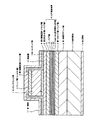
図1は、本発明によるGaInNAs系半導体発光装置、例えば半導体レーザ装置の一実施形態例の概略構成図である。
この実施の形態例においては、半導体基体1上に、順次第1導電型クラッド層2、第1のガイド層3、活性層領域層4、第2のガイド層5、第2導電型第1クラッド層6、エッチングストップ層7、第2導電型第2クラッド層8、第2導電型のキャップ層9が形成されて成る。
この活性層領域層4は、単層もしくは2層以上のGaInNAsによる半導体活性層41による量子井戸層と、この半導体活性層41を挟んで配置されるバリア層42及びバリア層ともなる上述した第1及び第2のガイド層3及び5が配置された構成を有する。
図1の例では、3層の量子井戸構造によるGaInNAs系半導体活性層41がバリア層41を介して積層されたMQW構造とされている。
An embodiment of a semiconductor light emitting device using a GaInNAs system, that is, GaInNAs or GaInNAsSb as a semiconductor active layer according to the present invention will be described. However, the present invention is not limited to this embodiment.
FIG. 1 is a schematic configuration diagram of an embodiment of a GaInNAs-based semiconductor light emitting device according to the present invention, for example, a semiconductor laser device.
In this embodiment, a first conductivity type cladding layer 2, a first guide layer 3, an active
The active
In the example of FIG. 1, an MQW structure in which a GaInNAs-based semiconductor
また、この実施形態例では、キャップ層9及び第2導電型第2クラッド層8が、主たる電流通路の形成部となる部分をストライプ状リッジ部として残してその両側を、エッチングストップ層7におけるエッチング速度の低下を利用して、クラッド層6に至る深さにエッチングして、このエッチング溝10G内に、絶縁層10を形成した構成とした場合である。
そして、キャップ層(コンタクト層)9上の絶縁層10に開口が形成され、この開口を通じてキャップ層9と、基体1の裏面とにそれぞれオーミックに第1及び第2の電極11及び12が被着されて成る。
Further, in this embodiment example, the cap layer 9 and the second conductivity type second cladding layer 8 are etched in the etching stop layer 7 on both sides of the main current path forming portion, leaving a portion as a stripe ridge portion. This is a case in which the
Then, an opening is formed in the
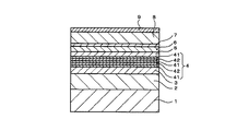
この半導体発光装置の実施形態例を、図1及び図2を参照して更に詳細に説明する。図2は、図1で示した半導体発光装置の半導体積層構造における断面図を示す。
この形態例では、半導体基体1として{100}結晶面からA面(Gaの配列面)方向にオフ角10°を有するGaAs基板を用いた場合である。また、第1導電型がn型で、第2導電型がp型とした場合である。
An example embodiment of the semiconductor light emitting device will be described in more detail with reference to FIGS. FIG. 2 is a cross-sectional view of the semiconductor stacked structure of the semiconductor light emitting device shown in FIG.
In this embodiment, a GaAs substrate having an off angle of 10 ° from the {100} crystal plane to the A plane (Ga alignment plane) direction is used as the
このGaAs基板による半導体基体1上に、順次例えば厚さ2μmのn型のAl0.47Ga0.53Asによる第1導電型クラッド層2、アンドープの厚さ約140nmのGaAsによる第1のガイド層3、厚さ8nmの量子井戸構造による3層のGaInNAs半導体活性層41と厚さ180nmのGaAsによるバリア層42との繰り返し積層による3QW構造の活性層領域層4、アンドープの厚さ140nmのGaAsによる第2のガイド層5、p型の厚さ100nmのAl0.47Ga0.53Asによる第2導電型第1クラッド層6、p型の厚さ100nmのGaAsによるエッチングストップ層7、p型の厚さ1.4μmのAl0.47Ga0.53Asによる第2導電型第2クラッド層8、p型の厚さ0.3μmのGaAsによるキャップ層9を、連続MOCVDによって積層形成する。
A first conductive cladding layer 2 made of n-type Al 0.47 Ga 0.53 As, for example, having a thickness of 2 μm, and a first guide made of undoped GaAs having a thickness of about 140 nm are sequentially formed on the
この積層半導体層を、キャップ層9側から、エッチングストップ層7の深さのエッチング溝10Gを形成し、この溝10G内に例えばSiO2絶縁層あるいはn型のGaAsによる電流阻止層10を形成して、半導体発光素子、すなわち半導体レーザ素子を形成する。
なお、この半導体発光素子は、複数個同時に共通の基体1上に配列形成し、上述した第1および第2電極の形成を行って、各素子に関して切断分離なされる。
An etching groove 10G having a depth of the etching stop layer 7 is formed on the laminated semiconductor layer from the cap layer 9 side, and a
A plurality of the semiconductor light emitting elements are simultaneously formed on the
このようにして、絶縁層10によって挟み込まれたストライプ部(リッジ)において主たる電流通路が形成され、このストライプ部下における活性層領域層4が発光機能部として動作するものであり、上述した切断分離において、ストライプ部の延長方向の長さの規定によって光共振器長の規定がなされる。すなわち、例えば350μmの共振器長となるストライプ部の長さに切断する。
In this way, a main current path is formed in the stripe portion (ridge) sandwiched between the
この光振器長の両端面の破断面は、例えば劈開面による鏡面によって構成することができる。そして、これら端面、すなわち共振器の端面は、所要の反射率を有する端面に設定する誘電体膜等が被着形成される。これら端面は、例えば主たる発光端面となる前方面においては反射率60%とされ、後方端面においては、例えば反射率95%とされる。 The fracture surface of both end faces of the optical vibrator length can be constituted by a mirror surface by a cleavage plane, for example. Then, a dielectric film or the like set on these end faces, that is, the end faces of the resonators, are set to end faces having a required reflectance. These end faces have, for example, a reflectance of 60% on the front surface which is the main light emitting end face, and have a reflectance of 95%, for example, on the rear end face.
上述した構成によって得た半導体発光装置においては、その発振波長が約1.47μmとなった。 そして、この半導体発光装置における活性層領域層4を、TEM(透過電子顕微鏡)によって観察したところ、組成変調構造が観察された。
これは、半導体基体1として、オフ基板を用いたことにより、半導体層の成長面に微視的に周期的段差が発生することによって、比較的原子移動すなわちマイグレーションが大きいInが段差部に偏析し、これによりこのInと結合しやすいAsとのInAsがリッチな微細領域によるIn優勢組成領域が形成され、他部領域に、Inによって阻害されることなくNが取り込まれたGaNの微細領域が配置された組成変調構造が生じるものと考えられる。
In the semiconductor light emitting device obtained by the above-described configuration, the oscillation wavelength is about 1.47 μm. And when the active layer area |
This is because the use of an off-substrate as the
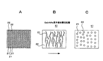
図3は、上述した活性層領域層4のGaInNAs系半導体活性層41における上述した組成変調構造の模式的断面図を示したもので、それぞれ活性層41の厚さ方向に渡るIn優勢組成領域21と、N優勢組成領域22とが活性層41の面方向に交互に配列される。
FIG. 3 is a schematic cross-sectional view of the above-described composition modulation structure in the GaInNAs-based semiconductor
尚、比較のために、上述した本発明による実施形態例と同様の構成によるものの、GaAs基板としてオフ基板によらない、いわゆるジャスト基板を用いた場合、組成変調構造を観察することができなかった。
これらの結果から、オフ基板を用いて組成変調構造を持たせることにより、GaInNAs系活性層による発光半導体装置、例えば半導体レーザの長波長化ができることがわかった。
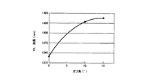
図4は、このオフ角とPL(Photo Luminescence)の波長との関係の測定結果を示すものである。これによれば、オフ角を上げることによって長波長化がなされる。因みに、オフ角10°において波長1.435μm程度が得られる成長条件と同じ条件でジャスト基板に成長した場合、PL波長1.33μm程度となった。つまり、組成変調構造を持つことにより、大幅に発光波長が長波化することがわかる。
For comparison, the composition modulation structure could not be observed when a so-called just substrate that does not depend on an off-substrate was used as the GaAs substrate, although it had the same configuration as the above-described embodiment according to the present invention. .
From these results, it was found that a light-emitting semiconductor device such as a semiconductor laser with a GaInNAs-based active layer can be made longer by providing a composition modulation structure using an off substrate.
FIG. 4 shows the measurement results of the relationship between the off angle and the PL (Photo Luminescence) wavelength. According to this, the wavelength is increased by increasing the off angle. Incidentally, when grown on a just substrate under the same growth conditions that a wavelength of about 1.435 μm was obtained at an off angle of 10 °, the PL wavelength was about 1.33 μm. That is, it can be seen that the emission wavelength is significantly increased by having the composition modulation structure.
しかしながら、上述した組成変調構造は、オフ基板を用いることによってのみ得られるものではなく、オフ角ゼロの例えば{100}基板によるいわゆるジャスト基体1を用いることができる。
例えばGaInNAs系半導体活性層41の成膜面のバリア層、図1及び図2の例ではバリア層42とガイド層3によるバリア層を、例えばGaInAs、AlGaInAs、AlGaInP、InGaP、GaNAs、GaAsP、InGaAsPより構成することによって、面内に歪分布を生じさせることができる。
これら材料は、組成によって歪量を変えることができることから、GaInNAs系半導体活性層の形成面のバリア層に、この材料層による歪量が相違する部分を形成して歪部分にInが偏析する特性を利用して、組成変調構造を形成することもできる。
However, the above-described composition modulation structure is not obtained only by using an off substrate, and a so-called just
For example, the barrier layer on the film-forming surface of the GaInNAs-based semiconductor
Since these materials can change the amount of strain depending on the composition, the barrier layer on the formation surface of the GaInNAs-based semiconductor active layer has a portion where the amount of strain due to this material layer is different, and In segregates in the strained portion. It is also possible to form a composition modulation structure using
また、歪みを局在させる構造としては、例えば上述したバリア層にInGaAsの量子ドットを形成する。この量子ドットの形成方法については、周知の方法によることができるものである。そして、このドットが存在する面に、例えばMQW構造において、バリア層としてのGaAs層を堆積成膜し、この上に活性層41を構成するGaInNAs層を堆積すると、ドットによる歪の局在部分が踏襲されてその形成面に存在することから、この歪みの局在部に原子移動(Migration)が大きいInの偏析、したがって、InAsが偏析するドット部を形成することができる。
As a structure for localizing strain, for example, InGaAs quantum dots are formed in the above-described barrier layer. About the formation method of this quantum dot, it can be based on a known method. Then, when a GaAs layer as a barrier layer is deposited on the surface where the dots exist, for example, in the MQW structure, and a GaInNAs layer constituting the
図5は、GaInNAs系半導体活性層41における、上述したように、In優勢組成領域21と、N優勢組成領域22のパターンを模式的に示した平面的で、上述した基体1として例えばオフ基板を用いることによって図5A及びBに示す帯状パターンを得たり、あるいは図5Cで示すように、前述したドットパターンとすることなど種々のパターンを得ることができる。
FIG. 5 is a plan view schematically showing the pattern of the In
尚、このIn偏析部21のパターン組成変調は、微細構造でかつそれほど組成の違いが大きくない方が良いものである。すなわち、この組成変調構造の周期が大きく、組成の違いも大きくなると、活性層領域層のバンドギャップの縮小部が生じるなどにより、発光光の吸収等の損失が生じて利得の低下を来たすことによる。
その周期と組成変調の組み合わせにより、最適値の選定がなされるが、例えば周期は、1μm以下とし、In組成の揺らぎは10%以下が望ましい。これは、ドットパターンにおいても同様である。
The pattern composition modulation of the In
The optimum value is selected according to the combination of the period and the composition modulation. For example, the period is preferably 1 μm or less, and the fluctuation of the In composition is preferably 10% or less. The same applies to the dot pattern.
上述した実施の形態例では、いわゆる端面発光型の半導体レーザ構造とした場合であるが、このような端面発光の半導体レーザへの適用に限定されるものではなく、面発光レーザ等に適用することもできる。図6は、本発明による垂直共振器面発光レーザ(VCSEL)の実施形態例の概略断面図である。
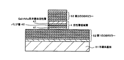
この面発光レーザにおいては、例えばGaAs基板からなる半導体基体51上に、通常の面発光半導体レーザにおけるように、第1及び第2のDBR(Distributed Bragg Reflector)ミラー52及び53と、これらに挟み込まれた例えばMQW構造の活性層領域層54を有して成る。この活性層領域層54は、例えば図5Cで示したパターン等のIn優勢組成領域21とN優勢組成領域22とが形成された、GaInNAs半導体活性層41による量子井戸層とバリア層42との例えばMQW構造を有する。
In the above-described embodiment, the so-called edge-emitting semiconductor laser structure is used. However, the present invention is not limited to application to such an edge-emitting semiconductor laser, and is applicable to a surface-emitting laser or the like. You can also. FIG. 6 is a schematic cross-sectional view of an example embodiment of a vertical cavity surface emitting laser (VCSEL) according to the present invention.
In this surface-emitting laser, for example, first and second DBR (Distributed Bragg Reflector) mirrors 52 and 53 are sandwiched between a semiconductor substrate 51 made of a GaAs substrate and the like, as in a normal surface-emitting semiconductor laser. For example, the active layer region layer 54 having an MQW structure is provided. This active layer region layer 54 includes, for example, a quantum well layer formed by a GaInNAs semiconductor
GaAs基板上に形成された面発光半導体レーザは、格子不整合が少なく、また、DBRミラーに適した材料として知られているAlGaAsによるミラーを適用することができる。
したがって、本発明による半導体発光装置における特有のGaInNAs半導体活性層による活性層領域層53による構成とするときは、発光効率の高い高品質の、長波長、すなわち1.3μm以上の半導体発光装置、この例においては、面発光半導体レーザを低価格で実現できるものである。
A surface emitting semiconductor laser formed on a GaAs substrate has few lattice mismatches, and an AlGaAs mirror known as a material suitable for a DBR mirror can be applied.
Therefore, when the semiconductor light emitting device according to the present invention is configured by the active layer region layer 53 by the unique GaInNAs semiconductor active layer, the semiconductor light emitting device having high emission efficiency and high quality, long wavelength, that is, 1.3 μm or more, In the example, the surface emitting semiconductor laser can be realized at a low price.
上述したように、本発明による半導体発光装置においては、そのGaInNAs系半導体層に組成変調構造を有することによって、InによるNの取り込みが阻害されることが回避されることから、GaInNAsあるいはGaInNAsSb層におけるNの取り込み効率を上げることができる。
そのため、MOCVDなどの成長方法によっても容易にNを取り込むことが可能になる。また、MBE法においても成長温度を高温化させることが可能になるため、この場合には、さらに高品質のGaInNAs系半導体層が成長できるようになる。
As described above, in the semiconductor light emitting device according to the present invention, since the GaInNAs-based semiconductor layer has a compositional modulation structure, it is avoided that N incorporation by In is inhibited, so that the GaInNAs or GaInNAsSb layer N uptake efficiency can be increased.
Therefore, N can be easily taken in even by a growth method such as MOCVD. Further, since the growth temperature can be increased also in the MBE method, in this case, a higher quality GaInNAs-based semiconductor layer can be grown.
そして、このように、Nの組成を容易に上げることができるということは、N原料を大量に流したり、結晶品質が悪くなるレベルまで成長温度を下げたりしなくても容易にGaInNAs系半導体層を成長できるようになるということである。つまり、成長条件の選定の範囲を広げることができる。
また、周期構造を持つことにより、同じ組成の混晶でも、波長が長波長化することが知られているが、このことから、通常のGaInNAs層よりも、より少ないInもしくはN組成で長波化か可能になる。
Thus, the fact that the composition of N can be easily increased means that a GaInNAs-based semiconductor layer can be easily formed without flowing a large amount of N raw material or lowering the growth temperature to a level at which the crystal quality deteriorates. It will be able to grow. That is, the range of selection of growth conditions can be expanded.
In addition, it is known that even with mixed crystals with the same composition, the wavelength is longer due to having a periodic structure, but this makes it longer with a smaller In or N composition than a normal GaInNAs layer. Or become possible.
また、本発明は、上述した構造の半導体発光装置に限定されるものではなく、各種の構造による半導体レーザ、半導体発光素子、また、単体半導体発光装置に適用する例に限定されるものではなく、多数の発光部を有する半導体発光装置、集積回路装置等に適用することもできるなど種々の装置に適用することができるものである。 Further, the present invention is not limited to the semiconductor light emitting device having the above-described structure, and is not limited to an example applied to a semiconductor laser, a semiconductor light emitting element, or a single semiconductor light emitting device having various structures, The present invention can be applied to various devices such as a semiconductor light emitting device having a large number of light emitting portions, an integrated circuit device, and the like.
1・・・半導体基体、2・・・第1導電型クラッド層、3・・・第1のガイド層、4・・・活性層領域層、41・・・GaInNAs系半導体活性層、42・・・バリア層、5・・・第2のガイド層、6・・・第2導電型第1クラッド層、7・・・エッチングストップ層、8・・・第2導電型第2クラッド層、9・・・キャップ層、10・・・電流阻止層、10G・・・エッチング溝、11・・・第1電極、12・・・第2電極、21・・・In優勢組成領域、22・・・N優勢組成領域、51・・・半導体基体、52・・・第1のDBRミラー、53・・・第2のDBRミラー
DESCRIPTION OF
Claims (10)
上記半導体発光素子の活性層領域層のGaInNAs系半導体活性層が、該半導体活性層の面方向にIn(インジウム)とN(窒素)の組成においてIn優勢組成領域とN優勢組成領域とが分布する組成変調構造を有することを特徴とする半導体発光装置。 A semiconductor light emitting device having a GaInNAs semiconductor light emitting element,
In the GaInNAs-based semiconductor active layer of the active layer region of the semiconductor light emitting device, an In dominant composition region and an N dominant composition region are distributed in the composition of In (indium) and N (nitrogen) in the plane direction of the semiconductor active layer. A semiconductor light-emitting device having a composition modulation structure.
該量子井戸層を挟むバリア層が局所的歪みを有することを特徴とする請求項1に記載の半導体発光装置。 The GaInNAs-based semiconductor active layer of the active layer region layer is composed of a single layer or a multilayer quantum well layer,
2. The semiconductor light emitting device according to claim 1, wherein the barrier layer sandwiching the quantum well layer has local strain.
上記N優勢組成領域が、平均組成よりNとGaが多い領域であることを特徴とする請求項1に記載の半導体発光装置。 The In dominant composition region is a region with more In and As than the average composition,
2. The semiconductor light emitting device according to claim 1, wherein the N dominant composition region is a region where N and Ga are larger than an average composition.
該量子井戸層を挟むバリア層が、GaInAs、AlGaInAs、AlGaInP、InGaP、GaNAs、GaAsP、InGaAsPより成ることを特徴とする請求項1に記載の半導体発光装置。 The GaInNAs-based semiconductor active layer of the active layer region layer is composed of a single layer or a multilayer quantum well layer,
2. The semiconductor light emitting device according to claim 1, wherein the barrier layer sandwiching the quantum well layer is made of GaInAs, AlGaInAs, AlGaInP, InGaP, GaNAs, GaAsP, or InGaAsP.
Priority Applications (1)
| Application Number | Priority Date | Filing Date | Title |
|---|---|---|---|
| JP2004048287A JP2005243720A (en) | 2004-02-24 | 2004-02-24 | Semiconductor light-emitting device |
Applications Claiming Priority (1)
| Application Number | Priority Date | Filing Date | Title |
|---|---|---|---|
| JP2004048287A JP2005243720A (en) | 2004-02-24 | 2004-02-24 | Semiconductor light-emitting device |
Publications (2)
| Publication Number | Publication Date |
|---|---|
| JP2005243720A true JP2005243720A (en) | 2005-09-08 |
| JP2005243720A5 JP2005243720A5 (en) | 2006-09-28 |
Family
ID=35025161
Family Applications (1)
| Application Number | Title | Priority Date | Filing Date |
|---|---|---|---|
| JP2004048287A Pending JP2005243720A (en) | 2004-02-24 | 2004-02-24 | Semiconductor light-emitting device |
Country Status (1)
| Country | Link |
|---|---|
| JP (1) | JP2005243720A (en) |
Cited By (4)
| Publication number | Priority date | Publication date | Assignee | Title |
|---|---|---|---|---|
| JP2009283801A (en) * | 2008-05-26 | 2009-12-03 | Nippon Telegr & Teleph Corp <Ntt> | Optical semiconductor device |
| WO2010134426A1 (en) * | 2009-05-19 | 2010-11-25 | 株式会社Qdレーザ | Semiconductor laser |
| US8483252B2 (en) | 2007-03-19 | 2013-07-09 | Fujitsu Limited | Semiconductor light emitting device and fabrication method for semiconductor light emitting device |
| JP5379002B2 (en) * | 2007-07-17 | 2013-12-25 | 株式会社Qdレーザ | Semiconductor laser and manufacturing method thereof |
-
2004
- 2004-02-24 JP JP2004048287A patent/JP2005243720A/en active Pending
Cited By (6)
| Publication number | Priority date | Publication date | Assignee | Title |
|---|---|---|---|---|
| US8483252B2 (en) | 2007-03-19 | 2013-07-09 | Fujitsu Limited | Semiconductor light emitting device and fabrication method for semiconductor light emitting device |
| US8802468B2 (en) | 2007-03-19 | 2014-08-12 | Fujitsu Limited | Semiconductor light emitting device and fabrication method for semiconductor light emitting device |
| JP5379002B2 (en) * | 2007-07-17 | 2013-12-25 | 株式会社Qdレーザ | Semiconductor laser and manufacturing method thereof |
| JP2009283801A (en) * | 2008-05-26 | 2009-12-03 | Nippon Telegr & Teleph Corp <Ntt> | Optical semiconductor device |
| WO2010134426A1 (en) * | 2009-05-19 | 2010-11-25 | 株式会社Qdレーザ | Semiconductor laser |
| JP2010272589A (en) * | 2009-05-19 | 2010-12-02 | Qd Laser Inc | Semiconductor laser |
Similar Documents
| Publication | Publication Date | Title |
|---|---|---|
| JP4594814B2 (en) | Photonic crystal laser, photonic crystal laser manufacturing method, surface emitting laser array, optical transmission system, and writing system | |
| JP3897186B2 (en) | Compound semiconductor laser | |
| JP7464643B2 (en) | Etched planarized VCSEL and method for making same - Patents.com | |
| US8906721B2 (en) | Semiconductor light emitting device and method for manufacturing the same | |
| EP1182756A2 (en) | Semiconductor laser device having lower threshold current | |
| EP0661782A1 (en) | A semiconductor laser | |
| JP3189791B2 (en) | Semiconductor laser | |
| US8802468B2 (en) | Semiconductor light emitting device and fabrication method for semiconductor light emitting device | |
| EP1553670B1 (en) | Semiconductor device having a quantum well structure including dual barrier layers, semiconductor laser employing the semiconductor device and methods of manufacturing the semiconductor device and the semiconductor laser. | |
| JP2799372B2 (en) | Quantum wire laser and manufacturing method thereof | |
| JP2004253802A (en) | GaAsSb/GaAs DEVICE WITH IMPROVED TEMPERATURE PROPERTY | |
| JP5381692B2 (en) | Semiconductor light emitting device | |
| JP2001223433A (en) | Vertical cavity semiconductor surface emission laser element and optical system using the same | |
| JP2008172188A (en) | Multi-wavelength quantum dot laser device | |
| JP2005243720A (en) | Semiconductor light-emitting device | |
| JP2005243720A5 (en) | ||
| JP2009076640A (en) | Semiconductor light emitting element | |
| JP2001358407A (en) | Semiconductor laser device | |
| JP2004087564A (en) | Semiconductor laser element and manufacturing method thereof | |
| JP2005294510A (en) | Semiconductor device | |
| WO2023281741A1 (en) | Semiconductor optical element | |
| JP2611509B2 (en) | Semiconductor laser | |
| JP2006216752A (en) | Manufacturing method for diffraction grating and semiconductor laser | |
| JP2000208872A (en) | Semiconductor element and its manufacture | |
| JPH0936472A (en) | Semiconductor laser element |
Legal Events
| Date | Code | Title | Description |
|---|---|---|---|
| A521 | Written amendment |
Free format text: JAPANESE INTERMEDIATE CODE: A523 Effective date: 20060810 |
|
| A621 | Written request for application examination |
Effective date: 20060810 Free format text: JAPANESE INTERMEDIATE CODE: A621 |
|
| A977 | Report on retrieval |
Free format text: JAPANESE INTERMEDIATE CODE: A971007 Effective date: 20091127 |
|
| A131 | Notification of reasons for refusal |
Free format text: JAPANESE INTERMEDIATE CODE: A131 Effective date: 20091208 |
|
| A02 | Decision of refusal |
Free format text: JAPANESE INTERMEDIATE CODE: A02 Effective date: 20100928 |