EP2169757A2 - Protection circuit module and secondary battery including the protection circuit module - Google Patents
Protection circuit module and secondary battery including the protection circuit module Download PDFInfo
- Publication number
- EP2169757A2 EP2169757A2 EP09252228A EP09252228A EP2169757A2 EP 2169757 A2 EP2169757 A2 EP 2169757A2 EP 09252228 A EP09252228 A EP 09252228A EP 09252228 A EP09252228 A EP 09252228A EP 2169757 A2 EP2169757 A2 EP 2169757A2
- Authority
- EP
- European Patent Office
- Prior art keywords
- fpcb
- pcm
- protection circuit
- bare cell
- circuit module
- Prior art date
- Legal status (The legal status is an assumption and is not a legal conclusion. Google has not performed a legal analysis and makes no representation as to the accuracy of the status listed.)
- Granted
Links
Images


Classifications
-
- H—ELECTRICITY
- H01—ELECTRIC ELEMENTS
- H01M—PROCESSES OR MEANS, e.g. BATTERIES, FOR THE DIRECT CONVERSION OF CHEMICAL ENERGY INTO ELECTRICAL ENERGY
- H01M50/00—Constructional details or processes of manufacture of the non-active parts of electrochemical cells other than fuel cells, e.g. hybrid cells
- H01M50/20—Mountings; Secondary casings or frames; Racks, modules or packs; Suspension devices; Shock absorbers; Transport or carrying devices; Holders
-
- H—ELECTRICITY
- H01—ELECTRIC ELEMENTS
- H01M—PROCESSES OR MEANS, e.g. BATTERIES, FOR THE DIRECT CONVERSION OF CHEMICAL ENERGY INTO ELECTRICAL ENERGY
- H01M10/00—Secondary cells; Manufacture thereof
- H01M10/42—Methods or arrangements for servicing or maintenance of secondary cells or secondary half-cells
-
- H—ELECTRICITY
- H01—ELECTRIC ELEMENTS
- H01M—PROCESSES OR MEANS, e.g. BATTERIES, FOR THE DIRECT CONVERSION OF CHEMICAL ENERGY INTO ELECTRICAL ENERGY
- H01M10/00—Secondary cells; Manufacture thereof
- H01M10/42—Methods or arrangements for servicing or maintenance of secondary cells or secondary half-cells
- H01M10/425—Structural combination with electronic components, e.g. electronic circuits integrated to the outside of the casing
-
- H—ELECTRICITY
- H01—ELECTRIC ELEMENTS
- H01M—PROCESSES OR MEANS, e.g. BATTERIES, FOR THE DIRECT CONVERSION OF CHEMICAL ENERGY INTO ELECTRICAL ENERGY
- H01M10/00—Secondary cells; Manufacture thereof
- H01M10/42—Methods or arrangements for servicing or maintenance of secondary cells or secondary half-cells
- H01M10/44—Methods for charging or discharging
-
- H—ELECTRICITY
- H01—ELECTRIC ELEMENTS
- H01M—PROCESSES OR MEANS, e.g. BATTERIES, FOR THE DIRECT CONVERSION OF CHEMICAL ENERGY INTO ELECTRICAL ENERGY
- H01M10/00—Secondary cells; Manufacture thereof
- H01M10/42—Methods or arrangements for servicing or maintenance of secondary cells or secondary half-cells
- H01M10/46—Accumulators structurally combined with charging apparatus
-
- H—ELECTRICITY
- H02—GENERATION; CONVERSION OR DISTRIBUTION OF ELECTRIC POWER
- H02J—ELECTRIC POWER NETWORKS; CIRCUIT ARRANGEMENTS OR SYSTEMS FOR SUPPLYING OR DISTRIBUTING ELECTRIC POWER; SYSTEMS FOR STORING ELECTRIC ENERGY
- H02J7/00—Circuit arrangements for charging or discharging batteries or for supplying loads from batteries
- H02J7/02—Circuit arrangements for charging or discharging batteries or for supplying loads from batteries for charging batteries from AC mains by converters
- H02J7/04—Regulation of charging current or voltage
-
- H—ELECTRICITY
- H05—ELECTRIC TECHNIQUES NOT OTHERWISE PROVIDED FOR
- H05K—PRINTED CIRCUITS; CASINGS OR CONSTRUCTIONAL DETAILS OF ELECTRIC APPARATUS; MANUFACTURE OF ASSEMBLAGES OF ELECTRICAL COMPONENTS
- H05K1/00—Printed circuits
- H05K1/18—Printed circuits structurally associated with non-printed electric components
- H05K1/189—Printed circuits structurally associated with non-printed electric components characterised by the use of flexible or folded printed circuits
-
- Y—GENERAL TAGGING OF NEW TECHNOLOGICAL DEVELOPMENTS; GENERAL TAGGING OF CROSS-SECTIONAL TECHNOLOGIES SPANNING OVER SEVERAL SECTIONS OF THE IPC; TECHNICAL SUBJECTS COVERED BY FORMER USPC CROSS-REFERENCE ART COLLECTIONS [XRACs] AND DIGESTS
- Y02—TECHNOLOGIES OR APPLICATIONS FOR MITIGATION OR ADAPTATION AGAINST CLIMATE CHANGE
- Y02E—REDUCTION OF GREENHOUSE GAS [GHG] EMISSIONS, RELATED TO ENERGY GENERATION, TRANSMISSION OR DISTRIBUTION
- Y02E60/00—Enabling technologies; Technologies with a potential or indirect contribution to GHG emissions mitigation
- Y02E60/10—Energy storage using batteries
Definitions
- the present invention relates to a secondary battery, and more particularly to a protection circuit module and a secondary battery including the same.
- PCMs protection circuit modules
- various circuit devices are mounted on a printed circuit board (PCB).
- PCB printed circuit board
- the invention sets out to provide a thin protection circuit module and a secondary battery including the same.
- the invention also sets out to provide a secondary battery that includes a protection circuit module that is thin and safely protects a circuit device.
- a protection circuit module for a secondary battery including a bare cell.
- the PCM includes: a flexible printed circuit board (FPCB); and control circuitry mounted on the FPCB and configured for electrical coupling to the bare cell through the FPCB, the control circuitry being adapted to control charging and discharging of the bare cell.
- FPCB flexible printed circuit board
- the control circuitry may be marked on the FPCB using an adhesive material.
- the control circuitry may include a controller and a switch including a first switching device and a second switching device.
- the adhesive material between the controller and the FPCB may be electrically insulating.
- a portion of the FPCB below the controller may have conductive material exposed to the adhesive material.
- the adhesive material between the switch and the FPCB may be electrically conductive.
- the adhesive material may have a thickness of about 0.03 mm or less. Further, the adhesive material may have a thickness of about 0.01 mm or less.
- the PCM may further include a plurality of first wire bonding pads on the FPCB around the controller, wherein the controller is electrically coupled to the first wire bonding pads via first wires; and a plurality of second wire bonding pads on the FPCB around the first and second switching devices, wherein the first and second switching devices are electrically coupled to the second wire bonding pads via second wires.
- Each of the wire bonding pads may include a conductive material on an exposed copper of the FPCB.
- the conductive material may include gold.
- Each of the wires may include a conductive material selected from the group consisting of gold, copper, aluminum, nickel, and combinations thereof.
- None of the wires may extend greater than about 0.2 mm above an IC chip of the controller. Each of the wires may extend about 0.1 mm or less above the IC chip of the controller.
- the PCM may further include a protector encapsulating the control circuitry on the FPCB.
- the protector may include a material selected from the group consisting of epoxy resin, silicon compound and combinations thereof.
- An upper end of the protector may be located about 0.1 mm or less above a highest point of wires between the control circuitry and the FPCB.
- the upper end of the protector may be located about 0.05 mm or less above the highest point of the wires between the control circuitry and the FPCB.
- a distance measured from a lower surface of the FPCB opposite an upper surface on which the control circuitry is mounted and the top of the protector may be about 0.5 mm or less.
- a secondary battery in another embodiment, includes a bare cell; and a protection circuit module (PCM) electrically coupled to the bare cell.
- the PCM includes: a flexible printed circuit board (FPCB); control circuitry mounted on the FPCB via adhesive material and electrically coupled to the bare cell through the FPCB, the control circuitry being adapted to control charging and discharging of the bare cell; and external terminals electrically coupled to the control circuitry via the FPCB and for electrically coupling the bare cell to an external device.
- FPCB flexible printed circuit board
- control circuitry mounted on the FPCB via adhesive material and electrically coupled to the bare cell through the FPCB, the control circuitry being adapted to control charging and discharging of the bare cell
- external terminals electrically coupled to the control circuitry via the FPCB and for electrically coupling the bare cell to an external device.
- the PCM in the secondary battery may have substantially the same features as the above described PCM.
- FIG. 1 is a block diagram illustrating a secondary battery including a protection circuit module according to an embodiment of the present invention
- FIG. 2 is a perspective view of the protection circuit module illustrated in FIG. 1 ;
- FIG. 3 is a perspective view of an electric circuit device on a semiconductor wafer used for the protection circuit module of FIG. 1 ;
- FIG. 4 is a plan view of the protection circuit module illustrated in FIG. 1 , and illustrates a section where a control IC and a switching device are mounted;
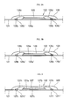
- FIG. 5A is a side view of the protection circuit module illustrated in FIG. 3 , and illustrates the control IC;
- FIG. 5B is a side view of the protection circuit module according to another embodiment of the present invention.
- FIG. 6 is a side view of the protection circuit module illustrated in FIG. 3 , and illustrates the switching device;
- FIG. 7 is a sectional view of the protection circuit module illustrated in FIGs. 3 and 4 that is taken along the line A-A of FIG. 4 ;
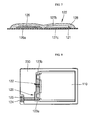
- FIG. 8 is a schematic perspective view of a core pack including the bare cell and the protection circuit module of the secondary battery according to one embodiment of the present invention.
- a secondary battery 100 includes a bare cell 110 and a protection circuit module (PCM) 120.
- the bare cell provides electric energy, and includes an electrode assembly, a can in which the electrode assembly and an electrolyte are received, and a cap assembly covering the can.
- the bare cell 110 includes a first electrode 111 and a second electrode 112.
- the first electrode 111 is a positive electrode and the second electrode 112 is a negative electrode, but the present invention is not limited thereto.
- a circuit formed in the protection circuit module 120 includes a first internal terminal 123a, a second internal terminal 123b, a first external terminal 124, a second external terminal 125, a controller 126, and a switch 127.
- the first internal terminal 123a is electrically connected to the first electrode 111 of the bare cell 110.
- the second internal terminal 123b is electrically connected to the second electrode 112.
- a charger or an external load may be electrically connected to the first external terminal 124 and the second external terminal 125.
- the controller 126 outputs a control signal to the switch 127 using voltage information of the bare cell 110.
- the switch 127 sets the direction of current so that only one of charge and discharge can be performed at a time, according to the control signal of the controller 126.
- the protection circuit module 120 controls overall operation including charge and discharge of the bare cell 110. Those skilled in the art would understand that the protection circuit module 120 may include other electric circuit components such as resistors, capacitors, and temperature fuses without being limited thereto.
- FIG. 2 illustrates the protection circuit module (PCM) 120 according to one embodiment of the present invention.
- the protection circuit module 120 includes a flexible printed circuit board (FPCB) 121 and a chip mount 122 provided on the FPCB 121.
- FPCB flexible printed circuit board
- the FPCB 121 is an elongated L-shaped strip in FIG. 2
- the present invention is not limited thereto.
- the FPCB may have an elongated rectangular shape (or stripe shape).
- the FPCB 121 includes the first internal terminal 123a, the second internal terminal 123b, the first external terminal 124, and the second external terminal 125.
- the FPCB 121 has a thickness of approximately 0.1 mm.
- the chip mount 122 includes the controller 126, the switch 127, and a protector 128.
- control circuitry The controller 126 and the switch 127 may together be referred to as "control circuitry.”
- the control circuitry is mounted on the FPCB 121 via adhesive material and configured for electrical coupling to the bare cell through the FPCB 121.
- the control circuitry is adapted to control charging and discharging of the bare cell 110.
- the controller 126 As illustrated in FIG. 3 , the controller 126 according to the described embodiment is implemented in a die type IC chip obtained from a semiconductor wafer 130.
- the IC chip 126 is mounted on the FPCB 121 such that its surface on which a terminal is formed faces upward.
- the thickness of the IC chip 126 is approximately 0.2 mm, for example.
- the IC chip 126 is coupled to the FPCB 121 by a first die bonding pad 126a formed on the FPCB 121.
- the first die bonding pad 126a may be formed by coating an adhesive material on the FPCB 121.
- an insulating epoxy resin is used as the first die bonding pad 126a.
- the first die bonding pad 126a may be made of conductive adhesive material.
- the thickness of the first die bonding pad 126a (i.e., the adhesive material) is approximately 0.03 mm, for example. In other embodiments, the thickness of the first die bonding pad 126a may be less than 0.03 mm. For example, the thickness of the first die bonding pad 126a may be 0.01 mm or less in some embodiments.
- the first die bonding pad 126a is larger than the IC chip 126 in the described embodiment.
- the first die bonding pad 126a has a shape similar to that of the IC chip 126.
- the ratio of dimensions between the first die bonding pad 126a and the IC chip 126 according to one embodiment is at least 1.2:1, but the present invention is not limited thereto. In other words, the length and width of the first die bonding pad 126a respectively are at least 1.2 times those of the IC chip 126 in one embodiment. In other embodiments, the ratio of dimensions may be more or less than 1.2.
- first wire bonding pads 126b spaced apart from the first die bonding pad 126a are disposed around the first die bonding pad 126a.
- the IC chip 126 is electrically coupled to the first wire bonding pads 126b via first wires 126c.
- each first wire bonding pad 126b is formed by plating a copper foil formed in the FPCB 121 with gold.
- an outer layer of the FPCB 121 is peeled to expose the underlying conductive layer (i.e., copper), and then gold is plated on it to form electrical contact.
- the copper foil may be plated with any other suitable conductive material.
- At least one of the first wires 126c is electrically connected to each first wire bonding pad 126b at one end by a method such as wire bonding.
- the width of the first wire bonding pad 126b in one embodiment is at least five times the diameter of the first wire 126c so that the first wire 126c can be easily connected to the first wire bonding pad 126b, but the present invention is not limited thereto.
- the other ends of the first wires 126c are electrically connected to terminals of the IC chip 126 by a method such as wire bonding.
- the upper ends of the first wires are located (or extend) not greater than approximately 0.2 mm above the IC chip 126 according to one embodiment. In other embodiments, the upper ends of the first wires may extend about 0.1 mm or less above the IC chip.
- the first wires 126c are made of gold, but the present invention is not limited thereto. In other embodiments, the first wires 126c may be made of a conductive material such as copper, aluminum, or nickel, as well as gold.
- the first die bonding pad 126a can be mounted on the FPCB 121 without peeling (or removing) the external insulating layer of the FPCB 121.
- the material used for the pad can be either a conductive material (e.g., conductive epoxy) or an insulating material (e.g., insulating epoxy resin) because an electrical short between the IC chip 126 and the FPCB 121 is unlikely because of the external insulating layer.
- the first wire bonding pads 126b are mounted on a portion of the FPCB 121 after peeling the external insulating layer to expose the underlying conductive material (e.g., copper foil.). Then a suitable conductive material (e.g., gold) is plated on the exposed conductive material of the FPCB 121 to form contacts 126b'. This way, electrical connections can be formed between the IC chip 126 and the FPCB 121 via the first wires 126c and the first wire bonding pads 126b.
- a suitable conductive material e.g., gold
- the material used for the first die bonding pad 126a should be insulating material (e.g., insulating epoxy resin) so that undesirable electrical connections (i.e., a short) between the IC chip 126 and the FPCB 121 can be prevented.
- insulating material e.g., insulating epoxy resin
- the switch 127 includes a first switching device 127a and a second switching device 127b.
- the switching devices 127a and 127b are field-effect transistors (FETs), but the present invention is not limited thereto. Any suitable device capable of performing a switching operation according to embodiments of the present invention may be used as the switching devices.
- the first switching device 127a and the second switching device 127b are die type FET chips obtained from a semiconductor wafer 130 similarly as the IC chip.
- the first FET chip 127a and the second FET chip 127b are mounted on the FPCB 121 such that their surfaces on which a gate terminal and a source terminal are formed face upward and their surfaces on which a drain terminal are formed face downward.
- the thickness of the FET chips 127a and 127b is approximately 0.18 mm, for example.
- the two FET chips 127a and 127b are mounted on and coupled to the FPCB 121 by a second die bonding pad 127c formed on the FPCB 121.
- the second die bonding pad 127c is formed by coating an adhesive material on the FPCB 121.
- a conductive material in particular, a conductive epoxy resin is used as the second die bonding pad 127c.
- the drain terminal of the first FET chip 127a and the drain terminal of the second FET chip 127b are electrically connected to each other through the second die bonding pad 127c.
- the thickness of the second die bonding pad 127c (i.e., the adhesive material) is approximately 0.03 mm in one embodiment. In other embodiments, the thickness of the second die bonding pad 127c may be less than 0.03 mm. In still other embodiments, the thickness of the second die bonding pad 127c may be about 0.01 mm or less.
- the area of the second die bonding pad 127 is larger than the total area of the two FETs 127a and 127b.
- the second die bonding pad 127c has a shape similar to the shape of the two FET chips 127a and 127b together, and the ratio of dimensions between the second die bonding pad 127 and the two FET chips 127a and 127b together according to one embodiment is at least 1.2:1, but the present invention is not limited thereto.
- the length and width of the second die bonding pad 127 respectively are at least 1.2 times those of the combined area of the FETs 127 and 127b.
- the ratios may be more or less than 1.2.
- Second, third, fourth, and fifth wire bonding pads 127d, 127e, 127f, and 127g spaced apart from the second die bonding pad 127c are disposed around the second die bonding pad 127c.
- the second wire bonding pad 127d and the third wire bonding pad 127e are located adjacent to the first FET chip 127a
- the fourth wire bonding pad 127f and the fifth wire bonding pad 127g are located adjacent to the second FET chip 127b.
- the second, third, fourth, and fifth wire bonding pads 127d, 127e, 127f, and 127g are formed by plating copper foil formed in the FPCB 121 with gold. In other embodiments, any other suitable material can be used to plate the copper foil.
- third, fourth, and fifth wires 127h, 127j, 127k, and 127m are electrically connected to the second, third, fourth, and fifth wire bonding pads 127d, 127e, 127f, and 127g, respectively, by a method such as wire bonding.
- the second wire 127h is electrically connected to a gate terminal of the first FET chip 127a by a method such as wire bonding.
- the third wire 127j is electrically connected to a source terminal of the first FET chip 127a by a method such as wire bonding.
- the fourth wire 127k is electrically connected to a gate terminal of the second FET chip 127b by a method such as wire bonding.
- the fifth wire 127m is electrically connected to a source terminal of the second FET chip 127b by a method such as wire bonding.
- the upper ends of the wires 127h, 127j, 127k, and 127m are located approximately 0.2 mm or less above the two FET chips 127a and 127b. In other embodiments, the upper ends of the wires 127h, 127j, 127k, and 127m may be located less than or equal to about 0.1 mm above the FET chips 127a and 127b.
- the second, third, fourth, and fifth wires 127h, 127j, 127k, and 127m are made of gold, but the present invention is not limited thereto.
- the wires 127h, 127j, 127k, and 127m may be made of other suitable conductive material such as copper, aluminum, or nickel, as well as gold.
- the switch 127 has the two switching devices 127a and 127b, but the present invention is not limited thereto.
- a device formed by integrating two switching devices i.e., a device in which two FETs are formed in one chip, may be used.
- the second and fourth wire bonding pads 127d, 127f are mounted on a portion of the FPCB 121 after peeling the external insulating layer to expose the underlying conductive material (e.g., copper foil.). While not shown in FIG. 6 , the third and fifth wire bonding pads 127e and 127g would similarly be mounted on the FPCB 121 after removing the underlying insulating layer. Then a suitable conductive material (e.g., gold) is plated on the exposed conductive material FPCB 121 to form the contacts 127d' and 127f shown in FIG. 6 .
- a suitable conductive material e.g., gold
- the protector 128 is a molded portion formed on the FPCB 121.
- the protector is formed by coating a protective material such that the IC chip 126, the first die bonding pad 126a, the two FET chips 127a and 127b, the second die bonding pad 127c, the wire bonding pads 126b, 127d, 127e, 127f, and 127g, and the wires 126c, 127h, 127j, 127k, and 127m are encapsulated therein.
- the protector is made of an epoxy resin, but the present invention is not limited thereto. In other words, the protector may be made of any other suitable material such as silicon.
- the upper end of the protector 128 is located approximately 0.1 mm or less above the upper ends of the wires 126b, 127d, 127e, 127f, and 127g. In one embodiment, the upper end of the protector is located about 0.05 mm or less above the highest point of the wires between the control circuitry (including the IC chip 126 and the switch 127) and the FPCB 121.
- the distance measured from a lower surface (i.e., the surface opposite the surface on which the chip mount is located) of the FPCB 121 and the top of the protector is about 0.5 mm or less.
- the protector 128 may be formed by dropping liquefied epoxy resin onto a corresponding region, for example. The protector 128 insulates the parts accommodated therein from the outside and prevents the wires from being circuit-shorted or broken by an external impact.
- the thickness of the FPCB 121 is approximately 0.1 mm
- the thickness of the die bonding pad 126a and 127c formed on the FPCB 121 is approximately 0.03 mm
- the thickness of the IC chip 126 that is the thickest chip mounted onto the die bonding pads 126a and 127c is approximately 0.22 mm.
- the wire 126c extends approximately 0.1 mm above the IC chip 126 and the upper end of the protector 128 is located approximately 0.05 mm above the upper end of the wire 126c.
- the protection circuit module 120 may be slimmed such that the total thickness thereof is approximately 0.5 mm.
- FIG. 8 is a schematic perspective view of a core pack 200 of the secondary battery 100 that includes the bare cell 110 and the protection circuit module 120.
- the protection circuit module 120 is mounted directly on the bare cell 110, so as to reduce the size of the resulting core pack 200.
- the protection circuit module 120 may be mounted on a hard material fixture for providing structural support to the FPCB 121.
Landscapes
- Engineering & Computer Science (AREA)
- Chemical & Material Sciences (AREA)
- Chemical Kinetics & Catalysis (AREA)
- Electrochemistry (AREA)
- General Chemical & Material Sciences (AREA)
- Manufacturing & Machinery (AREA)
- Microelectronics & Electronic Packaging (AREA)
- Power Engineering (AREA)
- Battery Mounting, Suspending (AREA)
- Charge And Discharge Circuits For Batteries Or The Like (AREA)
- Secondary Cells (AREA)
- Protection Of Static Devices (AREA)
Abstract
Description
- The present invention relates to a secondary battery, and more particularly to a protection circuit module and a secondary battery including the same.
- In recent years, due to the rapid development of communications and computer industries, the use of portable electronic devices has been increasing. Rechargeable secondary batteries are primarily being used as power sources for portable electronic devices.
- Secondary batteries that include protection circuit modules (PCMs) for controlling charge and discharge thereof are being widely used. Due to the rapid miniaturization of the portable electronic devices using secondary batteries as the main power source, it is desirable to further reduce the size of the secondary batteries. In a conventional protection circuit module, various circuit devices are mounted on a printed circuit board (PCB). However, since the thickness of a printed circuit board itself is at least 0.5 mm, there is a limit to decreasing the thickness of the conventional protection circuit modules.
- The invention sets out to provide a thin protection circuit module and a secondary battery including the same. The invention also sets out to provide a secondary battery that includes a protection circuit module that is thin and safely protects a circuit device.
- According to the present invention, a protection circuit module (PCM) for a secondary battery including a bare cell is provided. The PCM includes: a flexible printed circuit board (FPCB); and control circuitry mounted on the FPCB and configured for electrical coupling to the bare cell through the FPCB, the control circuitry being adapted to control charging and discharging of the bare cell.
- The control circuitry may be marked on the FPCB using an adhesive material.
- The control circuitry may include a controller and a switch including a first switching device and a second switching device.
- The adhesive material between the controller and the FPCB may be electrically insulating. A portion of the FPCB below the controller may have conductive material exposed to the adhesive material.
- The adhesive material between the switch and the FPCB may be electrically conductive.
- The adhesive material may have a thickness of about 0.03 mm or less. Further, the adhesive material may have a thickness of about 0.01 mm or less.
- The PCM may further include a plurality of first wire bonding pads on the FPCB around the controller, wherein the controller is electrically coupled to the first wire bonding pads via first wires; and a plurality of second wire bonding pads on the FPCB around the first and second switching devices, wherein the first and second switching devices are electrically coupled to the second wire bonding pads via second wires. Each of the wire bonding pads may include a conductive material on an exposed copper of the FPCB. The conductive material may include gold.
- Each of the wires may include a conductive material selected from the group consisting of gold, copper, aluminum, nickel, and combinations thereof.
- None of the wires may extend greater than about 0.2 mm above an IC chip of the controller. Each of the wires may extend about 0.1 mm or less above the IC chip of the controller.
- The PCM may further include a protector encapsulating the control circuitry on the FPCB. The protector may include a material selected from the group consisting of epoxy resin, silicon compound and combinations thereof. An upper end of the protector may be located about 0.1 mm or less above a highest point of wires between the control circuitry and the FPCB. The upper end of the protector may be located about 0.05 mm or less above the highest point of the wires between the control circuitry and the FPCB.
- A distance measured from a lower surface of the FPCB opposite an upper surface on which the control circuitry is mounted and the top of the protector may be about 0.5 mm or less.
- In another embodiment of the present invention, a secondary battery includes a bare cell; and a protection circuit module (PCM) electrically coupled to the bare cell. The PCM includes: a flexible printed circuit board (FPCB); control circuitry mounted on the FPCB via adhesive material and electrically coupled to the bare cell through the FPCB, the control circuitry being adapted to control charging and discharging of the bare cell; and external terminals electrically coupled to the control circuitry via the FPCB and for electrically coupling the bare cell to an external device.
- The PCM in the secondary battery may have substantially the same features as the above described PCM.
- The above and other features of the invention are set out in the appended claims
- The features and aspects of the present invention will be more apparent from the following detailed description in conjunction with the accompanying drawings, in which:
-
FIG. 1 is a block diagram illustrating a secondary battery including a protection circuit module according to an embodiment of the present invention; -
FIG. 2 is a perspective view of the protection circuit module illustrated inFIG. 1 ; -
FIG. 3 is a perspective view of an electric circuit device on a semiconductor wafer used for the protection circuit module ofFIG. 1 ; -
FIG. 4 is a plan view of the protection circuit module illustrated inFIG. 1 , and illustrates a section where a control IC and a switching device are mounted; -
FIG. 5A is a side view of the protection circuit module illustrated inFIG. 3 , and illustrates the control IC; -
FIG. 5B is a side view of the protection circuit module according to another embodiment of the present invention; -
FIG. 6 is a side view of the protection circuit module illustrated inFIG. 3 , and illustrates the switching device; -
FIG. 7 is a sectional view of the protection circuit module illustrated inFIGs. 3 and 4 that is taken along the line A-A ofFIG. 4 ; and -
FIG. 8 is a schematic perspective view of a core pack including the bare cell and the protection circuit module of the secondary battery according to one embodiment of the present invention. - Hereinafter, embodiments of the present invention will be described in detail with reference to the accompanying drawings.
- Referring to the block diagram of
FIG. 1 , asecondary battery 100 includes abare cell 110 and a protection circuit module (PCM) 120. The bare cell provides electric energy, and includes an electrode assembly, a can in which the electrode assembly and an electrolyte are received, and a cap assembly covering the can. Thebare cell 110 includes a first electrode 111 and asecond electrode 112. In the described embodiment, the first electrode 111 is a positive electrode and thesecond electrode 112 is a negative electrode, but the present invention is not limited thereto. - Referring to
FIG. 1 , a circuit formed in theprotection circuit module 120 includes a firstinternal terminal 123a, a secondinternal terminal 123b, a firstexternal terminal 124, a secondexternal terminal 125, acontroller 126, and aswitch 127. The firstinternal terminal 123a is electrically connected to the first electrode 111 of thebare cell 110. The secondinternal terminal 123b is electrically connected to thesecond electrode 112. For example, a charger or an external load may be electrically connected to the firstexternal terminal 124 and the secondexternal terminal 125. Thecontroller 126 outputs a control signal to theswitch 127 using voltage information of thebare cell 110. In one embodiment, theswitch 127 sets the direction of current so that only one of charge and discharge can be performed at a time, according to the control signal of thecontroller 126. - The
protection circuit module 120 controls overall operation including charge and discharge of thebare cell 110. Those skilled in the art would understand that theprotection circuit module 120 may include other electric circuit components such as resistors, capacitors, and temperature fuses without being limited thereto. -
FIG. 2 illustrates the protection circuit module (PCM) 120 according to one embodiment of the present invention. Referring toFIG. 2 , theprotection circuit module 120 includes a flexible printed circuit board (FPCB) 121 and achip mount 122 provided on theFPCB 121. Although theFPCB 121 is an elongated L-shaped strip inFIG. 2 , the present invention is not limited thereto. By way of example, in other embodiments, the FPCB may have an elongated rectangular shape (or stripe shape). As discussed above, theFPCB 121 includes the firstinternal terminal 123a, the secondinternal terminal 123b, the firstexternal terminal 124, and the secondexternal terminal 125. TheFPCB 121 has a thickness of approximately 0.1 mm. Thechip mount 122 includes thecontroller 126, theswitch 127, and aprotector 128. - The
controller 126 and theswitch 127 may together be referred to as "control circuitry." In one embodiment, the control circuitry is mounted on theFPCB 121 via adhesive material and configured for electrical coupling to the bare cell through theFPCB 121. The control circuitry is adapted to control charging and discharging of thebare cell 110. - As illustrated in
FIG. 3 , thecontroller 126 according to the described embodiment is implemented in a die type IC chip obtained from asemiconductor wafer 130. - Referring to
FIGs. 4 ,5A ,5B , and7 , theIC chip 126 is mounted on theFPCB 121 such that its surface on which a terminal is formed faces upward. The thickness of theIC chip 126 is approximately 0.2 mm, for example. TheIC chip 126 is coupled to theFPCB 121 by a firstdie bonding pad 126a formed on theFPCB 121. The firstdie bonding pad 126a may be formed by coating an adhesive material on theFPCB 121. In one embodiment, an insulating epoxy resin is used as the firstdie bonding pad 126a. In other embodiments, the firstdie bonding pad 126a may be made of conductive adhesive material. - The thickness of the first
die bonding pad 126a (i.e., the adhesive material) is approximately 0.03 mm, for example. In other embodiments, the thickness of the firstdie bonding pad 126a may be less than 0.03 mm. For example, the thickness of the firstdie bonding pad 126a may be 0.01 mm or less in some embodiments. - The first
die bonding pad 126a is larger than theIC chip 126 in the described embodiment. For convenience of mounting, the firstdie bonding pad 126a has a shape similar to that of theIC chip 126. The ratio of dimensions between the firstdie bonding pad 126a and theIC chip 126 according to one embodiment is at least 1.2:1, but the present invention is not limited thereto. In other words, the length and width of the firstdie bonding pad 126a respectively are at least 1.2 times those of theIC chip 126 in one embodiment. In other embodiments, the ratio of dimensions may be more or less than 1.2. - In the embodiment illustrated in
FIG. 4 , four firstwire bonding pads 126b spaced apart from the firstdie bonding pad 126a are disposed around the firstdie bonding pad 126a. TheIC chip 126 is electrically coupled to the firstwire bonding pads 126b viafirst wires 126c. - In one embodiment, each first
wire bonding pad 126b is formed by plating a copper foil formed in theFPCB 121 with gold. In other words, an outer layer of theFPCB 121 is peeled to expose the underlying conductive layer (i.e., copper), and then gold is plated on it to form electrical contact. In other embodiments, the copper foil may be plated with any other suitable conductive material. - At least one of the
first wires 126c is electrically connected to each firstwire bonding pad 126b at one end by a method such as wire bonding. The width of the firstwire bonding pad 126b in one embodiment is at least five times the diameter of thefirst wire 126c so that thefirst wire 126c can be easily connected to the firstwire bonding pad 126b, but the present invention is not limited thereto. - The other ends of the
first wires 126c are electrically connected to terminals of theIC chip 126 by a method such as wire bonding. When thefirst wires 126c are connected to the terminals formed on the upper surface of theIC chip 126, the upper ends of the first wires are located (or extend) not greater than approximately 0.2 mm above theIC chip 126 according to one embodiment. In other embodiments, the upper ends of the first wires may extend about 0.1 mm or less above the IC chip. - In one embodiment, the
first wires 126c are made of gold, but the present invention is not limited thereto. In other embodiments, thefirst wires 126c may be made of a conductive material such as copper, aluminum, or nickel, as well as gold. - As can be seen in
FIG. 5A , the firstdie bonding pad 126a can be mounted on theFPCB 121 without peeling (or removing) the external insulating layer of theFPCB 121. In this case, the material used for the pad can be either a conductive material (e.g., conductive epoxy) or an insulating material (e.g., insulating epoxy resin) because an electrical short between theIC chip 126 and theFPCB 121 is unlikely because of the external insulating layer. - It can be seen in
FIG. 5A that the firstwire bonding pads 126b are mounted on a portion of theFPCB 121 after peeling the external insulating layer to expose the underlying conductive material (e.g., copper foil.). Then a suitable conductive material (e.g., gold) is plated on the exposed conductive material of theFPCB 121 to formcontacts 126b'. This way, electrical connections can be formed between theIC chip 126 and theFPCB 121 via thefirst wires 126c and the firstwire bonding pads 126b. - In other embodiments, as can be seen in
FIG. 5B , when the insulating layer of theFPCB 121 is removed to expose the conductive material (e.g., copper foil) 126a', the material used for the firstdie bonding pad 126a should be insulating material (e.g., insulating epoxy resin) so that undesirable electrical connections (i.e., a short) between theIC chip 126 and theFPCB 121 can be prevented. - Referring to
FIGs. 4 ,6 , and7 , theswitch 127 includes afirst switching device 127a and asecond switching device 127b. In one embodiment of the present invention, theswitching devices first switching device 127a and thesecond switching device 127b are die type FET chips obtained from asemiconductor wafer 130 similarly as the IC chip. - The
first FET chip 127a and thesecond FET chip 127b are mounted on theFPCB 121 such that their surfaces on which a gate terminal and a source terminal are formed face upward and their surfaces on which a drain terminal are formed face downward. The thickness of theFET chips - The two
FET chips FPCB 121 by a seconddie bonding pad 127c formed on theFPCB 121. The seconddie bonding pad 127c is formed by coating an adhesive material on theFPCB 121. In one embodiment of the present invention, a conductive material, in particular, a conductive epoxy resin is used as the seconddie bonding pad 127c. Using the seconddie bonding pad 127c made of a conductive material, the drain terminal of thefirst FET chip 127a and the drain terminal of thesecond FET chip 127b are electrically connected to each other through the seconddie bonding pad 127c. - The thickness of the second
die bonding pad 127c (i.e., the adhesive material) is approximately 0.03 mm in one embodiment. In other embodiments, the thickness of the seconddie bonding pad 127c may be less than 0.03 mm. In still other embodiments, the thickness of the seconddie bonding pad 127c may be about 0.01 mm or less. The area of the seconddie bonding pad 127 is larger than the total area of the twoFETs - For convenience of mounting, the second
die bonding pad 127c has a shape similar to the shape of the twoFET chips die bonding pad 127 and the twoFET chips die bonding pad 127 respectively are at least 1.2 times those of the combined area of theFETs - Second, third, fourth, and fifth
wire bonding pads die bonding pad 127c are disposed around the seconddie bonding pad 127c. The secondwire bonding pad 127d and the thirdwire bonding pad 127e are located adjacent to thefirst FET chip 127a, and the fourthwire bonding pad 127f and the fifthwire bonding pad 127g are located adjacent to thesecond FET chip 127b. In one embodiment, the second, third, fourth, and fifthwire bonding pads FPCB 121 with gold. In other embodiments, any other suitable material can be used to plate the copper foil. - Second, third, fourth, and
fifth wires wire bonding pads second wire 127h is electrically connected to a gate terminal of thefirst FET chip 127a by a method such as wire bonding. Thethird wire 127j is electrically connected to a source terminal of thefirst FET chip 127a by a method such as wire bonding. Thefourth wire 127k is electrically connected to a gate terminal of thesecond FET chip 127b by a method such as wire bonding. Thefifth wire 127m is electrically connected to a source terminal of thesecond FET chip 127b by a method such as wire bonding. - In one embodiment, when the
wires FET chips wires FET chips wires FET chips fifth wires wires - In one embodiment of the present invention, the
switch 127 has the twoswitching devices - It can be seen in
FIG. 6 that the second and fourthwire bonding pads FPCB 121 after peeling the external insulating layer to expose the underlying conductive material (e.g., copper foil.). While not shown inFIG. 6 , the third and fifthwire bonding pads FPCB 121 after removing the underlying insulating layer. Then a suitable conductive material (e.g., gold) is plated on the exposedconductive material FPCB 121 to form thecontacts 127d' and 127f shown inFIG. 6 . This way, electrical connections can be formed between theFETs FPCB 121 via the respective second, third, fourth andfifth wires wire bonding pads - Referring to
FIGs. 2 and 4 to 7 , theprotector 128 is a molded portion formed on theFPCB 121. The protector is formed by coating a protective material such that theIC chip 126, the firstdie bonding pad 126a, the twoFET chips die bonding pad 127c, thewire bonding pads wires - In one embodiment of the present invention, the protector is made of an epoxy resin, but the present invention is not limited thereto. In other words, the protector may be made of any other suitable material such as silicon. In one embodiment, the upper end of the
protector 128 is located approximately 0.1 mm or less above the upper ends of thewires IC chip 126 and the switch 127) and theFPCB 121. In some embodiments, the distance measured from a lower surface (i.e., the surface opposite the surface on which the chip mount is located) of theFPCB 121 and the top of the protector is about 0.5 mm or less. Theprotector 128 may be formed by dropping liquefied epoxy resin onto a corresponding region, for example. Theprotector 128 insulates the parts accommodated therein from the outside and prevents the wires from being circuit-shorted or broken by an external impact. - In one embodiment, the thickness of the
FPCB 121 is approximately 0.1 mm, the thickness of thedie bonding pad FPCB 121 is approximately 0.03 mm, and the thickness of theIC chip 126 that is the thickest chip mounted onto thedie bonding pads wire 126c extends approximately 0.1 mm above theIC chip 126 and the upper end of theprotector 128 is located approximately 0.05 mm above the upper end of thewire 126c. According to embodiments of the present invention, theprotection circuit module 120 may be slimmed such that the total thickness thereof is approximately 0.5 mm. -
FIG. 8 is a schematic perspective view of acore pack 200 of thesecondary battery 100 that includes thebare cell 110 and theprotection circuit module 120. As can be seen inFIG. 8 , theprotection circuit module 120 is mounted directly on thebare cell 110, so as to reduce the size of the resultingcore pack 200. In some embodiments, theprotection circuit module 120 may be mounted on a hard material fixture for providing structural support to theFPCB 121. - Although certain embodiments of the present invention have been described in detail hereinabove, it should be understood that many variations and modifications of the basic inventive concept herein described, which may appear to those skilled in the art, will still fall within the scope of the present invention as defined by the appended claims.
Claims (13)
- A protection circuit module (PCM) for a secondary battery comprising a bare cell, the PCM comprising:a flexible printed circuit board (FPCB); andcontrol circuitry mounted on the FPCB and configured for electrical coupling to the bare cell through the FPCB, the control circuitry being adapted to control charging and discharging of the bare cell.
- A PCM according to claim 1, wherein the control circuitry is marked on the FPCB using an adhesive material.
- A PCM according to claim 2, wherein the control circuitry comprises a controller and a switch comprising a first switching device and a second switching device.
- A PCM according to claim 3, wherein the adhesive material between the controller and the FPCB is electrically insulating.
- A PCM according to claim 4, wherein a portion of the FPCB below the controller has conductive material exposed to the adhesive material.
- A PCM according to claim 3, wherein the adhesive material between the switch and the FPCB is electrically conductive.
- A PCM according to any one of claims 3 to 6, further comprising a plurality of first wire bonding pads on the FPCB around the controller, wherein the controller is electrically coupled to the first wire bonding pads via first wires; and a plurality of second wire bonding pads on the FPCB around the first and second switching devices, wherein the first and second switching devices are electrically coupled to the second wire bonding pads via second wires.
- A PCM according to claim 7 wherein each of the wire bonding pads comprises a conductive material on an exposed conductive material of the FPCB.
- The PCM according to claim 8 wherein the conductive material of the bonding pads comprises gold.
- A PCM according to claim 7, 8 or 9 wherein each of the wires comprises a conductive material selected from the group consisting of gold, copper, aluminum, nickel, and combinations thereof.
- A PCM according to any preceding claim, further comprising a protector encapsulating the control circuitry on the FPCB.
- A PCM according to claim 11, wherein the protector comprises a material selected from the group consisting of epoxy resin, silicon compound and combinations thereof.
- A secondary battery comprising:a bare cell;a protection circuit module (PCM) electrically coupled to the bare cell, the PCM comprising the features of one of claims 1 to 12 and external terminals electrically coupled to the control circuitry via the FPCB and for electrically coupling the bare cell to an external device.
Applications Claiming Priority (2)
| Application Number | Priority Date | Filing Date | Title |
|---|---|---|---|
| US9821508P | 2008-09-18 | 2008-09-18 | |
| US12/548,302 US8547068B2 (en) | 2008-09-18 | 2009-08-26 | Protection circuit module and secondary battery including the protection circuit module |
Publications (3)
| Publication Number | Publication Date |
|---|---|
| EP2169757A2 true EP2169757A2 (en) | 2010-03-31 |
| EP2169757A3 EP2169757A3 (en) | 2012-04-25 |
| EP2169757B1 EP2169757B1 (en) | 2015-08-26 |
Family
ID=41401747
Family Applications (1)
| Application Number | Title | Priority Date | Filing Date |
|---|---|---|---|
| EP09252228.3A Active EP2169757B1 (en) | 2008-09-18 | 2009-09-18 | Protection circuit module and secondary battery including the protection circuit module |
Country Status (5)
| Country | Link |
|---|---|
| US (1) | US8547068B2 (en) |
| EP (1) | EP2169757B1 (en) |
| JP (1) | JP5356959B2 (en) |
| KR (1) | KR101075359B1 (en) |
| CN (1) | CN101677142A (en) |
Cited By (3)
| Publication number | Priority date | Publication date | Assignee | Title |
|---|---|---|---|---|
| EP2385568A3 (en) * | 2010-05-03 | 2015-04-22 | Samsung SDI Co., Ltd. | Protection circuit module and rechargeable battery including the same |
| EP3327826A1 (en) * | 2016-11-29 | 2018-05-30 | Samsung SDI Co., Ltd. | A bus bar for the electrical connection of at least two terminals of a battery system and a corresponding battery system |
| EP4220815A1 (en) * | 2022-01-27 | 2023-08-02 | Samsung SDI Co., Ltd. | Battery pack connector |
Families Citing this family (12)
| Publication number | Priority date | Publication date | Assignee | Title |
|---|---|---|---|---|
| CN102055180A (en) * | 2011-01-21 | 2011-05-11 | 天津长荣印刷设备股份有限公司 | Flexible protection circuit used for battery |
| BR112013018674A8 (en) * | 2011-01-25 | 2018-02-06 | Koninklijke Philips Nv | BATTERY ADAPTER AND METHOD OF MANUFACTURING A BATTERY ADAPTER |
| WO2011103833A2 (en) * | 2011-04-18 | 2011-09-01 | 华为终端有限公司 | Battery, battery component and subscriber equipment |
| US20130101871A1 (en) * | 2011-10-20 | 2013-04-25 | Bohyun Byun | Protective circuit module and battery pack having the same |
| KR101646826B1 (en) * | 2013-09-30 | 2016-08-08 | 주식회사 엘지화학 | Curved PCM |
| KR102434771B1 (en) | 2015-08-28 | 2022-08-22 | 삼성에스디아이 주식회사 | Battery pack |
| US9809446B1 (en) * | 2016-05-09 | 2017-11-07 | Amkor Technology, Inc. | Semiconductor package and manufacturing method thereof |
| JP6638710B2 (en) * | 2016-10-14 | 2020-01-29 | 株式会社デンソー | Battery device |
| US10741882B2 (en) * | 2018-07-09 | 2020-08-11 | Ford Global Technologies, Llc | Flex lead on cell container for electromagnetic shielding |
| WO2020048352A1 (en) * | 2018-09-04 | 2020-03-12 | 宁波舜宇光电信息有限公司 | Tof camera module, electronic device, and assembly method |
| EP4399763A4 (en) | 2021-09-10 | 2025-07-09 | Milwaukee Electric Tool Corp | BATTERY PACK |
| KR102758667B1 (en) * | 2022-01-04 | 2025-01-22 | 삼성에스디아이 주식회사 | Battery pack connector |
Family Cites Families (21)
| Publication number | Priority date | Publication date | Assignee | Title |
|---|---|---|---|---|
| JPS6143461A (en) | 1984-08-08 | 1986-03-03 | Hitachi Ltd | Thin film multilayer interconnection substrate |
| JPS61207045A (en) | 1985-03-11 | 1986-09-13 | Nec Corp | Resin-sealed semiconductor device |
| KR970000214B1 (en) | 1993-11-18 | 1997-01-06 | 삼성전자 주식회사 | Semiconductor device and method of producing the same |
| US5472804A (en) * | 1994-12-01 | 1995-12-05 | Motorola, Inc. | Battery device with integrated circuit substrate packaging |
| JPH11265960A (en) | 1998-03-18 | 1999-09-28 | Hitachi Chem Co Ltd | Semiconductor device with metal reinforcement |
| JP2001143672A (en) | 1999-11-16 | 2001-05-25 | Toshiba Battery Co Ltd | Integrated structure of battery and protection circuit board, and protection circuit board used therefor |
| JP3650008B2 (en) * | 2000-09-04 | 2005-05-18 | 三洋電機株式会社 | Protection circuit device using MOSFET and manufacturing method thereof |
| JP3966686B2 (en) | 2000-11-30 | 2007-08-29 | ソニーケミカル&インフォメーションデバイス株式会社 | Connecting material |
| JP3739708B2 (en) | 2002-01-10 | 2006-01-25 | 京セラ株式会社 | battery |
| JP4194420B2 (en) | 2003-05-27 | 2008-12-10 | 三洋電機株式会社 | Battery pack with overcurrent protection circuit |
| KR20070021981A (en) | 2003-09-09 | 2007-02-23 | 소니 케미카루 앤드 인포메이션 디바이스 가부시키가이샤 | Electronic component mounting module |
| US8778529B2 (en) | 2004-11-29 | 2014-07-15 | Samsung Sdi Co., Ltd. | Lithium secondary battery |
| US7612439B2 (en) | 2005-12-22 | 2009-11-03 | Alpha And Omega Semiconductor Limited | Semiconductor package having improved thermal performance |
| JP2006210409A (en) * | 2005-01-25 | 2006-08-10 | Mitsumi Electric Co Ltd | Battery protection module |
| KR100943594B1 (en) * | 2006-03-27 | 2010-02-24 | 삼성에스디아이 주식회사 | Protection circuit module and battery pack using same |
| JP2007266067A (en) | 2006-03-27 | 2007-10-11 | Mitsumi Electric Co Ltd | Flex / rigid board, secondary battery protection module, battery pack, and flex / rigid board manufacturing method |
| KR100797693B1 (en) | 2006-05-24 | 2008-01-23 | 삼성전기주식회사 | Manufacturing method of chip embedded printed circuit board |
| KR100760784B1 (en) * | 2006-07-04 | 2007-09-20 | 삼성에스디아이 주식회사 | Secondary battery protection circuit module and battery pack using same |
| KR20080048097A (en) | 2006-11-28 | 2008-06-02 | 삼성테크윈 주식회사 | Flexible package and manufacturing method thereof |
| KR100813626B1 (en) | 2006-12-20 | 2008-03-14 | 삼성전자주식회사 | Stacked Semiconductor Device Package |
| KR100779505B1 (en) | 2007-05-16 | 2007-11-27 | 에스맥 (주) | Printed circuit board with holes for inserting electronic components |
-
2009
- 2009-08-26 US US12/548,302 patent/US8547068B2/en active Active
- 2009-09-01 KR KR1020090082157A patent/KR101075359B1/en active Active
- 2009-09-14 JP JP2009211541A patent/JP5356959B2/en active Active
- 2009-09-17 CN CN200910173574A patent/CN101677142A/en active Pending
- 2009-09-18 EP EP09252228.3A patent/EP2169757B1/en active Active
Cited By (5)
| Publication number | Priority date | Publication date | Assignee | Title |
|---|---|---|---|---|
| EP2385568A3 (en) * | 2010-05-03 | 2015-04-22 | Samsung SDI Co., Ltd. | Protection circuit module and rechargeable battery including the same |
| US9136522B2 (en) | 2010-05-03 | 2015-09-15 | Samsung Sdi Co., Ltd. | Protection circuit module and rechargeable battery including the same |
| EP3327826A1 (en) * | 2016-11-29 | 2018-05-30 | Samsung SDI Co., Ltd. | A bus bar for the electrical connection of at least two terminals of a battery system and a corresponding battery system |
| EP4220815A1 (en) * | 2022-01-27 | 2023-08-02 | Samsung SDI Co., Ltd. | Battery pack connector |
| US12327883B2 (en) | 2022-01-27 | 2025-06-10 | Samsung Sdi Co., Ltd. | Battery pack connector |
Also Published As
| Publication number | Publication date |
|---|---|
| US8547068B2 (en) | 2013-10-01 |
| US20100066307A1 (en) | 2010-03-18 |
| EP2169757A3 (en) | 2012-04-25 |
| CN101677142A (en) | 2010-03-24 |
| JP2010073692A (en) | 2010-04-02 |
| EP2169757B1 (en) | 2015-08-26 |
| KR101075359B1 (en) | 2011-10-19 |
| JP5356959B2 (en) | 2013-12-04 |
| KR20100032821A (en) | 2010-03-26 |
Similar Documents
| Publication | Publication Date | Title |
|---|---|---|
| EP2169757B1 (en) | Protection circuit module and secondary battery including the protection circuit module | |
| US10263238B2 (en) | Battery protection circuit module package, battery pack and electronic device including same | |
| US8966749B2 (en) | Manufacturing method for protection circuit module of secondary battery | |
| TWI241714B (en) | Semiconductor device and switching element | |
| CN101599551B (en) | Battery pack | |
| US6610923B1 (en) | Multi-chip module utilizing leadframe | |
| US10193193B2 (en) | Structure of battery protection circuit module package coupled with holder, and battery pack having same | |
| KR20130043565A (en) | Protective circuit module and battery pack having the same | |
| TW486923B (en) | Protecting circuit device using MOSFET and preparing method therefor | |
| CN101752596A (en) | Secondary battery | |
| CN112218444B (en) | Battery protection circuit package and manufacturing method thereof | |
| KR20140115756A (en) | Protection apparatus of battery pack and method for manufacturing the same and battery pack having the same | |
| KR101434224B1 (en) | Battery protection circuits and package of battery protection circuits module | |
| KR20160025310A (en) | Package of battery protection circuits | |
| US6654218B1 (en) | Protection circuit module for rechargeable battery and method of making the same | |
| KR20150134128A (en) | Removable battery protection circuits package from holder and holder for removable to battery protection circuits package, battery pack including the same | |
| CN116709640B (en) | Circuit board assemblies and electronic devices | |
| KR20130080331A (en) | Package module of battery protection circuits | |
| KR101595501B1 (en) | Package of battery protection circuits module and battery pack | |
| US11831067B2 (en) | Electronic apparatus and method of manufacturing electronic apparatus | |
| JP3557143B2 (en) | Switching element bare chip mounting structure | |
| KR101582952B1 (en) | Package of battery protection circuits and battery pack | |
| CN116896824A (en) | Battery protection board module, method, device, battery module and electronic device | |
| KR20150010857A (en) | Holder to be equipped with battery protection circuits module package, method of fabricating the same, and method of fabricating battery pack using the same | |
| JP2001203220A (en) | Switching element bare chip mounting structure |
Legal Events
| Date | Code | Title | Description |
|---|---|---|---|
| PUAI | Public reference made under article 153(3) epc to a published international application that has entered the european phase |
Free format text: ORIGINAL CODE: 0009012 |
|
| 17P | Request for examination filed |
Effective date: 20090929 |
|
| AK | Designated contracting states |
Kind code of ref document: A2 Designated state(s): AT BE BG CH CY CZ DE DK EE ES FI FR GB GR HR HU IE IS IT LI LT LU LV MC MK MT NL NO PL PT RO SE SI SK SM TR |
|
| AX | Request for extension of the european patent |
Extension state: AL BA RS |
|
| PUAL | Search report despatched |
Free format text: ORIGINAL CODE: 0009013 |
|
| AK | Designated contracting states |
Kind code of ref document: A3 Designated state(s): AT BE BG CH CY CZ DE DK EE ES FI FR GB GR HR HU IE IS IT LI LT LU LV MC MK MT NL NO PL PT RO SE SI SK SM TR |
|
| AX | Request for extension of the european patent |
Extension state: AL BA RS |
|
| RIC1 | Information provided on ipc code assigned before grant |
Ipc: H01M 10/42 20060101AFI20120320BHEP |
|
| 17Q | First examination report despatched |
Effective date: 20130508 |
|
| GRAP | Despatch of communication of intention to grant a patent |
Free format text: ORIGINAL CODE: EPIDOSNIGR1 |
|
| INTG | Intention to grant announced |
Effective date: 20150312 |
|
| RIN1 | Information on inventor provided before grant (corrected) |
Inventor name: KIM, BONGYOUNG |
|
| GRAS | Grant fee paid |
Free format text: ORIGINAL CODE: EPIDOSNIGR3 |
|
| GRAA | (expected) grant |
Free format text: ORIGINAL CODE: 0009210 |
|
| AK | Designated contracting states |
Kind code of ref document: B1 Designated state(s): AT BE BG CH CY CZ DE DK EE ES FI FR GB GR HR HU IE IS IT LI LT LU LV MC MK MT NL NO PL PT RO SE SI SK SM TR |
|
| REG | Reference to a national code |
Ref country code: GB Ref legal event code: FG4D |
|
| REG | Reference to a national code |
Ref country code: CH Ref legal event code: EP |
|
| REG | Reference to a national code |
Ref country code: AT Ref legal event code: REF Ref document number: 745658 Country of ref document: AT Kind code of ref document: T Effective date: 20150915 |
|
| REG | Reference to a national code |
Ref country code: IE Ref legal event code: FG4D |
|
| REG | Reference to a national code |
Ref country code: DE Ref legal event code: R096 Ref document number: 602009033141 Country of ref document: DE |
|
| REG | Reference to a national code |
Ref country code: AT Ref legal event code: MK05 Ref document number: 745658 Country of ref document: AT Kind code of ref document: T Effective date: 20150826 |
|
| REG | Reference to a national code |
Ref country code: LT Ref legal event code: MG4D |
|
| PG25 | Lapsed in a contracting state [announced via postgrant information from national office to epo] |
Ref country code: GR Free format text: LAPSE BECAUSE OF FAILURE TO SUBMIT A TRANSLATION OF THE DESCRIPTION OR TO PAY THE FEE WITHIN THE PRESCRIBED TIME-LIMIT Effective date: 20151127 Ref country code: LV Free format text: LAPSE BECAUSE OF FAILURE TO SUBMIT A TRANSLATION OF THE DESCRIPTION OR TO PAY THE FEE WITHIN THE PRESCRIBED TIME-LIMIT Effective date: 20150826 Ref country code: NO Free format text: LAPSE BECAUSE OF FAILURE TO SUBMIT A TRANSLATION OF THE DESCRIPTION OR TO PAY THE FEE WITHIN THE PRESCRIBED TIME-LIMIT Effective date: 20151126 Ref country code: FI Free format text: LAPSE BECAUSE OF FAILURE TO SUBMIT A TRANSLATION OF THE DESCRIPTION OR TO PAY THE FEE WITHIN THE PRESCRIBED TIME-LIMIT Effective date: 20150826 Ref country code: LT Free format text: LAPSE BECAUSE OF FAILURE TO SUBMIT A TRANSLATION OF THE DESCRIPTION OR TO PAY THE FEE WITHIN THE PRESCRIBED TIME-LIMIT Effective date: 20150826 |
|
| REG | Reference to a national code |
Ref country code: NL Ref legal event code: MP Effective date: 20150826 |
|
| PG25 | Lapsed in a contracting state [announced via postgrant information from national office to epo] |
Ref country code: PT Free format text: LAPSE BECAUSE OF FAILURE TO SUBMIT A TRANSLATION OF THE DESCRIPTION OR TO PAY THE FEE WITHIN THE PRESCRIBED TIME-LIMIT Effective date: 20151228 Ref country code: AT Free format text: LAPSE BECAUSE OF FAILURE TO SUBMIT A TRANSLATION OF THE DESCRIPTION OR TO PAY THE FEE WITHIN THE PRESCRIBED TIME-LIMIT Effective date: 20150826 Ref country code: ES Free format text: LAPSE BECAUSE OF FAILURE TO SUBMIT A TRANSLATION OF THE DESCRIPTION OR TO PAY THE FEE WITHIN THE PRESCRIBED TIME-LIMIT Effective date: 20150826 Ref country code: SE Free format text: LAPSE BECAUSE OF FAILURE TO SUBMIT A TRANSLATION OF THE DESCRIPTION OR TO PAY THE FEE WITHIN THE PRESCRIBED TIME-LIMIT Effective date: 20150826 Ref country code: HR Free format text: LAPSE BECAUSE OF FAILURE TO SUBMIT A TRANSLATION OF THE DESCRIPTION OR TO PAY THE FEE WITHIN THE PRESCRIBED TIME-LIMIT Effective date: 20150826 Ref country code: IS Free format text: LAPSE BECAUSE OF FAILURE TO SUBMIT A TRANSLATION OF THE DESCRIPTION OR TO PAY THE FEE WITHIN THE PRESCRIBED TIME-LIMIT Effective date: 20151226 Ref country code: PL Free format text: LAPSE BECAUSE OF FAILURE TO SUBMIT A TRANSLATION OF THE DESCRIPTION OR TO PAY THE FEE WITHIN THE PRESCRIBED TIME-LIMIT Effective date: 20150826 |
|
| PG25 | Lapsed in a contracting state [announced via postgrant information from national office to epo] |
Ref country code: NL Free format text: LAPSE BECAUSE OF FAILURE TO SUBMIT A TRANSLATION OF THE DESCRIPTION OR TO PAY THE FEE WITHIN THE PRESCRIBED TIME-LIMIT Effective date: 20150826 |
|
| PG25 | Lapsed in a contracting state [announced via postgrant information from national office to epo] |
Ref country code: SK Free format text: LAPSE BECAUSE OF FAILURE TO SUBMIT A TRANSLATION OF THE DESCRIPTION OR TO PAY THE FEE WITHIN THE PRESCRIBED TIME-LIMIT Effective date: 20150826 Ref country code: DK Free format text: LAPSE BECAUSE OF FAILURE TO SUBMIT A TRANSLATION OF THE DESCRIPTION OR TO PAY THE FEE WITHIN THE PRESCRIBED TIME-LIMIT Effective date: 20150826 Ref country code: EE Free format text: LAPSE BECAUSE OF FAILURE TO SUBMIT A TRANSLATION OF THE DESCRIPTION OR TO PAY THE FEE WITHIN THE PRESCRIBED TIME-LIMIT Effective date: 20150826 Ref country code: IT Free format text: LAPSE BECAUSE OF FAILURE TO SUBMIT A TRANSLATION OF THE DESCRIPTION OR TO PAY THE FEE WITHIN THE PRESCRIBED TIME-LIMIT Effective date: 20150826 Ref country code: CZ Free format text: LAPSE BECAUSE OF FAILURE TO SUBMIT A TRANSLATION OF THE DESCRIPTION OR TO PAY THE FEE WITHIN THE PRESCRIBED TIME-LIMIT Effective date: 20150826 |
|
| REG | Reference to a national code |
Ref country code: CH Ref legal event code: PL |
|
| REG | Reference to a national code |
Ref country code: DE Ref legal event code: R097 Ref document number: 602009033141 Country of ref document: DE |
|
| PG25 | Lapsed in a contracting state [announced via postgrant information from national office to epo] |
Ref country code: MC Free format text: LAPSE BECAUSE OF FAILURE TO SUBMIT A TRANSLATION OF THE DESCRIPTION OR TO PAY THE FEE WITHIN THE PRESCRIBED TIME-LIMIT Effective date: 20150826 Ref country code: RO Free format text: LAPSE BECAUSE OF FAILURE TO SUBMIT A TRANSLATION OF THE DESCRIPTION OR TO PAY THE FEE WITHIN THE PRESCRIBED TIME-LIMIT Effective date: 20150826 |
|
| REG | Reference to a national code |
Ref country code: IE Ref legal event code: MM4A |
|
| PLBE | No opposition filed within time limit |
Free format text: ORIGINAL CODE: 0009261 |
|
| STAA | Information on the status of an ep patent application or granted ep patent |
Free format text: STATUS: NO OPPOSITION FILED WITHIN TIME LIMIT |
|
| PG25 | Lapsed in a contracting state [announced via postgrant information from national office to epo] |
Ref country code: LI Free format text: LAPSE BECAUSE OF NON-PAYMENT OF DUE FEES Effective date: 20150930 Ref country code: CH Free format text: LAPSE BECAUSE OF NON-PAYMENT OF DUE FEES Effective date: 20150930 Ref country code: IE Free format text: LAPSE BECAUSE OF NON-PAYMENT OF DUE FEES Effective date: 20150918 |
|
| 26N | No opposition filed |
Effective date: 20160530 |
|
| REG | Reference to a national code |
Ref country code: FR Ref legal event code: PLFP Year of fee payment: 8 |
|
| PG25 | Lapsed in a contracting state [announced via postgrant information from national office to epo] |
Ref country code: SI Free format text: LAPSE BECAUSE OF FAILURE TO SUBMIT A TRANSLATION OF THE DESCRIPTION OR TO PAY THE FEE WITHIN THE PRESCRIBED TIME-LIMIT Effective date: 20150826 |
|
| PG25 | Lapsed in a contracting state [announced via postgrant information from national office to epo] |
Ref country code: BE Free format text: LAPSE BECAUSE OF FAILURE TO SUBMIT A TRANSLATION OF THE DESCRIPTION OR TO PAY THE FEE WITHIN THE PRESCRIBED TIME-LIMIT Effective date: 20150826 |
|
| PG25 | Lapsed in a contracting state [announced via postgrant information from national office to epo] |
Ref country code: MT Free format text: LAPSE BECAUSE OF FAILURE TO SUBMIT A TRANSLATION OF THE DESCRIPTION OR TO PAY THE FEE WITHIN THE PRESCRIBED TIME-LIMIT Effective date: 20150826 |
|
| PG25 | Lapsed in a contracting state [announced via postgrant information from national office to epo] |
Ref country code: BG Free format text: LAPSE BECAUSE OF FAILURE TO SUBMIT A TRANSLATION OF THE DESCRIPTION OR TO PAY THE FEE WITHIN THE PRESCRIBED TIME-LIMIT Effective date: 20150826 Ref country code: HU Free format text: LAPSE BECAUSE OF FAILURE TO SUBMIT A TRANSLATION OF THE DESCRIPTION OR TO PAY THE FEE WITHIN THE PRESCRIBED TIME-LIMIT; INVALID AB INITIO Effective date: 20090918 Ref country code: SM Free format text: LAPSE BECAUSE OF FAILURE TO SUBMIT A TRANSLATION OF THE DESCRIPTION OR TO PAY THE FEE WITHIN THE PRESCRIBED TIME-LIMIT Effective date: 20150826 |
|
| PG25 | Lapsed in a contracting state [announced via postgrant information from national office to epo] |
Ref country code: CY Free format text: LAPSE BECAUSE OF FAILURE TO SUBMIT A TRANSLATION OF THE DESCRIPTION OR TO PAY THE FEE WITHIN THE PRESCRIBED TIME-LIMIT Effective date: 20150826 |
|
| REG | Reference to a national code |
Ref country code: FR Ref legal event code: PLFP Year of fee payment: 9 |
|
| PG25 | Lapsed in a contracting state [announced via postgrant information from national office to epo] |
Ref country code: TR Free format text: LAPSE BECAUSE OF FAILURE TO SUBMIT A TRANSLATION OF THE DESCRIPTION OR TO PAY THE FEE WITHIN THE PRESCRIBED TIME-LIMIT Effective date: 20150826 |
|
| PG25 | Lapsed in a contracting state [announced via postgrant information from national office to epo] |
Ref country code: LU Free format text: LAPSE BECAUSE OF NON-PAYMENT OF DUE FEES Effective date: 20150918 |
|
| PG25 | Lapsed in a contracting state [announced via postgrant information from national office to epo] |
Ref country code: MK Free format text: LAPSE BECAUSE OF FAILURE TO SUBMIT A TRANSLATION OF THE DESCRIPTION OR TO PAY THE FEE WITHIN THE PRESCRIBED TIME-LIMIT Effective date: 20150826 |
|
| REG | Reference to a national code |
Ref country code: FR Ref legal event code: PLFP Year of fee payment: 10 |
|
| P01 | Opt-out of the competence of the unified patent court (upc) registered |
Effective date: 20230528 |
|
| PGFP | Annual fee paid to national office [announced via postgrant information from national office to epo] |
Ref country code: DE Payment date: 20250902 Year of fee payment: 17 |
|
| PGFP | Annual fee paid to national office [announced via postgrant information from national office to epo] |
Ref country code: GB Payment date: 20250904 Year of fee payment: 17 |
|
| PGFP | Annual fee paid to national office [announced via postgrant information from national office to epo] |
Ref country code: FR Payment date: 20250908 Year of fee payment: 17 |