EP2169555A1 - Cache controller, cache control method and cache control program - Google Patents
Cache controller, cache control method and cache control program Download PDFInfo
- Publication number
- EP2169555A1 EP2169555A1 EP07767302A EP07767302A EP2169555A1 EP 2169555 A1 EP2169555 A1 EP 2169555A1 EP 07767302 A EP07767302 A EP 07767302A EP 07767302 A EP07767302 A EP 07767302A EP 2169555 A1 EP2169555 A1 EP 2169555A1
- Authority
- EP
- European Patent Office
- Prior art keywords
- data
- stored
- store data
- cache memory
- write address
- Prior art date
- Legal status (The legal status is an assumption and is not a legal conclusion. Google has not performed a legal analysis and makes no representation as to the accuracy of the status listed.)
- Withdrawn
Links
Images








Classifications
-
- G—PHYSICS
- G06—COMPUTING OR CALCULATING; COUNTING
- G06F—ELECTRIC DIGITAL DATA PROCESSING
- G06F12/00—Accessing, addressing or allocating within memory systems or architectures
- G06F12/02—Addressing or allocation; Relocation
- G06F12/08—Addressing or allocation; Relocation in hierarchically structured memory systems, e.g. virtual memory systems
- G06F12/0802—Addressing of a memory level in which the access to the desired data or data block requires associative addressing means, e.g. caches
- G06F12/0804—Addressing of a memory level in which the access to the desired data or data block requires associative addressing means, e.g. caches with main memory updating
-
- G—PHYSICS
- G06—COMPUTING OR CALCULATING; COUNTING
- G06F—ELECTRIC DIGITAL DATA PROCESSING
- G06F11/00—Error detection; Error correction; Monitoring
- G06F11/07—Responding to the occurrence of a fault, e.g. fault tolerance
- G06F11/08—Error detection or correction by redundancy in data representation, e.g. by using checking codes
- G06F11/10—Adding special bits or symbols to the coded information, e.g. parity check, casting out 9's or 11's
- G06F11/1008—Adding special bits or symbols to the coded information, e.g. parity check, casting out 9's or 11's in individual solid state devices
- G06F11/1064—Adding special bits or symbols to the coded information, e.g. parity check, casting out 9's or 11's in individual solid state devices in cache or content addressable memories
-
- G—PHYSICS
- G06—COMPUTING OR CALCULATING; COUNTING
- G06F—ELECTRIC DIGITAL DATA PROCESSING
- G06F12/00—Accessing, addressing or allocating within memory systems or architectures
- G06F12/02—Addressing or allocation; Relocation
- G06F12/08—Addressing or allocation; Relocation in hierarchically structured memory systems, e.g. virtual memory systems
- G06F12/0802—Addressing of a memory level in which the access to the desired data or data block requires associative addressing means, e.g. caches
- G06F12/0844—Multiple simultaneous or quasi-simultaneous cache accessing
- G06F12/0855—Overlapped cache accessing, e.g. pipeline
-
- G—PHYSICS
- G06—COMPUTING OR CALCULATING; COUNTING
- G06F—ELECTRIC DIGITAL DATA PROCESSING
- G06F2212/00—Indexing scheme relating to accessing, addressing or allocation within memory systems or architectures
- G06F2212/10—Providing a specific technical effect
- G06F2212/1032—Reliability improvement, data loss prevention, degraded operation etc
Definitions
- the present invention relates to a cache controller, a cache controlling method, and a cache controlling program that perform a write operation to store data received from an execution unit, and generate an ECC for the store data.
- a data cache memory protects data by appending an Error-Check-and-Correction (ECC) byte to an 8-byte data.
- ECC Error-Check-and-Correction
- An ECC is stored in an ECC cache memory (ECC-RAM) that is separate from DATA-RAM, and dedicatedly provided for ECCs.
- the ECC-RAM is updated when a register or a write operation is performed to the cache memory.
- an instruction processor issues a store instruction to a memory processor.
- the memory processor checks if the cache line to be stored is in the cache memory, and at the same time, reads the data in the cache line to be stored from the cache memory and checks the data for an error.
- store data issued from an execution unit and alike is written in a store buffer (STB).
- the memory processor When the instruction processor issues a store permission subsequently, the memory processor writes the data taken out from the store buffer into a write buffer (WB), and further writes the data taken out from the write buffer into the DATA-RAM.
- WB write buffer
- the memory processor generates an ECC based on 8-byte fetched data read from the DATA-RAM, using bytes-not-to-be-stored included therein (ECC generation 1).
- ECC generation 2 ECC based on data in the bytes-to-be-stored included in the 8-byte store data
- the memory processor then merges these two ECCs to generate an ECC corresponding to the updated store data, and stores the generated ECC in the ECC-RAM.
- a 1-bit error might be different in each of these scenarios, that is, in the data read from the DATA-RAM upon checking for an error when the retrieval access is made to the cache memory in response to the store request; and in the data read therefrom upon generating the ECC after the storing is permitted, and the cache memory is accessed for the write.
- the ECC corresponding to the data after the write cannot be generated properly.
- the ECC remaining at this point is one corresponding to the data before the write, and the data before the write has been already lost.
- a disclosed technique executes an error check and an ECC generation based on a single read (see FIG. 18 ).
- the disclosed memory processor does not use the data read from DATA-RAM upon executing the write.
- an ECC is generated based on the data stored previously, and the ECC is appended to the store data written in the STB, to generate new store data (see Patent Documents 1 to 4).
- An object of the present invention is to provide a cache controller, a cache controlling method, and a cache controlling program that are capable of preventing SSI from occurring even when equal to or less than 8-byte data is stored consecutively to the same address, and capable of generating a correct ECC.
- the invention set forth in claim 1 is a cache memory controller for writing store data received from an execution unit into a cache memory and generating an ECC for the store data.
- the cache memory controller includes a data detecting unit that detects a write address in the cache memory into which the store data is stored, an area-to-be-stored of the store data that is to be stored and an area-not-to-be-stored that is not to be stored, when the store data is transmitted from the execution unit; a data determining unit that determines whether data-to-be-stored that is already written is present in the write address detected by the data detecting unit; an existing data-not-to-be-stored obtaining unit that obtains, from the data written in the write address, data detected by the data detecting unit and written in the area-not-to-be-stored, as existing data-not-to-be-stored, when the data determining unit determines that the data-to-be-stored is present in the write address; a store
- the invention set forth in claim 2 further includes a data re-detecting unit that, when the data determining unit determines that no data-to-be-stored is present in the write address of the cache memory, detects data-already-stored already stored in the address of the cache memory detected by the data detecting unit after registering the data-to-be-stored thereto, wherein when the data re-detecting unit detects the data-already-stored already stored in the write address of the cache memory, the store data writing unit merges the new store data with the data-already-stored to generate further new store data, and writes the further new store data in the write address detected by the data detecting unit, and the ECC generating unit generates an ECC for the further new store data written by the store data writing unit into the cache memory, from the further new store data generated by the store data writing unit.
- the data detecting unit when the store data is transmitted from the execution unit, the data detecting unit further detects a write address of a cache memory into which preceding store data transmitted from the execution unit prior to the store data is to be stored, and a preceding area-to-be-stored that is to be stored in the preceding store data, the data determining unit further determines whether the write address of the store data detected by the data detecting unit makes a match with the write address of the preceding store data, when the data determining unit determines that the write address of the store data makes a match with the write address of the preceding store data, the store data writing unit merges the existing data-not-to-be-stored, the data-to-be-stored, and the preceding data-to-be-stored in the preceding area-to-be-stored detected by the data detecting unit to generate new store data, and writes the new store data into the write address in the cache memory, and the ECC generating unit generates an ECC for new data written by the store data writing unit
- the invention set forth in claim 4 is a cache memory controlling method suitable for writing store data received from an execution unit into a cache memory and generating an ECC for the store data.
- the cache memory controlling method includes a data detecting step of detecting a write address in the cache memory into which the store data is stored, an area-to-be-stored of the store data that is to be stored and an area-not-to-be-stored that is not to be stored, when the store data is transmitted from the execution unit; a data determining step of determining whether data-to-be-stored that is already written is present in the write address detected at the data detecting step; an existing data-not-to-be-stored obtaining step of obtaining, from the data written in the write address, data detected at the data detecting step and written in the area-not-to-be-stored, as existing data-not-to-be-stored, when it is determined that the data-to-be-stored is present in the write address at the data determining step; a store data writing step
- the invention set forth in claim 5 further includes a data re-detecting step of, when it is determined that no data-to-be-stored is present in the write address of the cache memory at the data determining step, detecting data-already-stored already stored in the address of the cache memory detected at the data detecting step after registering the data-to-be-stored thereto, wherein the store data writing step, when the data-already-stored already stored in the write address of the cache memory is detected, includes merging the new store data with the data-already-stored to generate further new store data, and writing the further new store data in the write address detected at the data detecting step, and the ECC generating step includes generating an ECC for the further new store data written at the store data writing step into the cache memory, from the further new store data generated at the store data writing step.
- the data detecting step when the store data is transmitted from the execution unit, includes further detecting a write address of a cache memory into which preceding store data transmitted from the execution unit prior to the store data is to be stored, and a preceding area-to-be-stored that is to be stored in the preceding store data
- the data determining step includes further determining whether the write address of the store data detected at the data detecting step makes a match with the write address of the preceding store data
- the store data writing step when it is determined that the write address of the store data makes a match with the write address of the preceding store data at the data determining step, includes merging the existing data-not-to-be-stored, the data-to-be-stored, and the preceding data-to-be-stored in the preceding area-to-be-stored detected at the data detecting step to generate new store data, and writing the new store data into the write address in the cache memory
- the ECC generating step includes generating an ECC for new
- the invention set forth in claim 7 is a cache memory controlling program that causes a computer to write store data received from an execution unit into a cache memory and generate an ECC for the store data.
- the cache memory controlling program includes a data detecting step of detecting a write address in the cache memory into which the store data is stored, an area-to-be-stored of the store data that is to be stored and an area-not-to-be-stored that is not to be stored, when the store data is transmitted from the execution unit; a data determining step of determining whether data-to-be-stored that is already written is present in the write address detected at the data detecting step; an existing data-not-to-be-stored obtaining step of obtaining, from the data written in the write address, data detected at the data detecting step and written in the area-not-to-be-stored, as existing data-not-to-be-stored, when it is determined that the data-to-be-stored is present in the write address at the data determining step; a store
- the invention set forth in claim 8 further includes a data re-detecting step of, when it is determined that no data-to-be-stored is present in the write address of the cache memory at the data determining step, detecting data-already-stored already stored in the address of the cache memory detected at the data detecting step after registering the data-to-be-stored thereto after registering the data-to-be-stored thereto, wherein the store data writing step, when the data-already-stored already stored in the write address of the cache memory is detected, includes merging the new store data with the data-already-stored to generate further new store data, and writing the further new store data in the write address detected at the data detecting step, and the ECC generating step includes generating an ECC for the further new store data written at the store data writing step into the cache memory, from the further new store data generated at the store data writing step.
- the data detecting step when the store data is transmitted from the execution unit, includes further detecting a write address of a cache memory into which preceding store data transmitted from the execution unit prior to the store data is to be stored, and a preceding area-to-be-stored that is to be stored in the preceding store data
- the data determining step includes further determining whether the write address of the store data detected at the data detecting step makes a match with the write address of the preceding store data
- the store data writing step when it is determined that the write address of the store data makes a match with the write address of the preceding store data at the data determining step, includes merging the existing data-not-to-be-stored, the data-to-be-stored, and the preceding data-to-be-stored in the preceding area-to-be-stored detected at the data detecting step to generate new store data, and writing the new store data into the write address in the cache memory
- the ECC generating step includes generating an ECC for new
- the data detecting unit upon receiving store data from the execution unit, detects a write address in a cache memory into which the store data is stored, an area-to-be-stored that is to be stored in the store data, and an area-not-to-be-stored that is not to be stored from the store data; the data determining unit determines whether any data-to-be-stored is already written in the detected write address; when the data determining unit determines that the data-to-be-stored is present in the write address, the existing data-not-to-be-stored obtaining unit obtains data written in the detected area-not-to-be-stored from the data written in the write address as existing data-not-to-be-stored; the store data writing unit merges the obtained existing data-not-to-be-stored with the data-to-be-stored in the detected area-to-be-stored to generate new store data, and writes the new store data in the detected write address; and the ECC generating unit generates an E
- the data re-detecting unit detects data-already-stored already stored in the detected address of the cache memory; when the data re-detecting unit detects the data-already-stored already stored in the write address in the cache memory, the store data writing unit merges the new store data with the data-already-stored to generate further new store data, and writes the further new store data in the write address detected by the data detecting unit; and the ECC generating unit generates an ECC for further new store data written in the cache memory, based the generated further new store data. Therefore, a correct ECC can be generated even when a cache miss occurs.
- the data detecting unit upon receiving store data from the execution unit, the data detecting unit further detects a write address in a cache memory in which preceding store data received from the execution unit prior to the store data is to be stored, and a preceding area-to-be-stored that is to be stored in the preceding store data; the data determining unit further determines whether the detected write address for the store data makes a match with the write address for the preceding store data; when the data determining unit determines that the write address for the store data makes a match with the write address for the preceding store data, the store data writing unit merges the existing data-not-to-be-stored with the data-to-be-stored and the preceding data-to-be-stored in the detected preceding area-to-be-stored to generate new store data, and writes the new store data in the write address in the cache memory; and the ECC generating unit generates an ECC for the new data written in the cache memory, based on the generated new store data.
- the cache memory controlling unit can generate new store data and an ECC taking preceding store data into consideration.
- SSI can be prevented from occurring more reliably even when equal to or less than 8-byte data is stored consecutively to the same address, and a correct ECC can be generated more surely.
- FIG. 1 is a schematic of a system structure depicting an entire structure of a cache memory controller according to a first embodiment of the present invention.
- FIG. 1 is a schematic of a system structure depicting an entire structure of the cache memory controller according to a first embodiment of the present invention.
- this cache memory controller is connected to an execution unit and an instruction processing unit to realize a central processing unit (CPU or MPU).
- the central processing unit is connected to a memory controlling unit that reads or writes data from or to a main memory.
- the instruction processing unit connected to a cache memory controlling unit transmits a store instruction appended with store-related information such as a store address, a store data width, and aligning information to the cache memory controlling unit.
- the execution unit transmits 8-byte store data to the cache memory controlling unit.
- the cache memory controlling unit includes: a plurality of store buffers (STB) that stores therein 8-byte store data transmitted by the execution unit; a plurality of write buffers (WB) that temporarily maintains the store data to be stored (to be written) in a DATA-RAM; the DATA-RAM that is a cache memory that stores therein 8-byte store data; a plurality of fetch data registers (FCDR) that maintains data output from the DATA-RAM; and an ECC-RAM that stores therein an ECC corresponding to 8-byte store data to be stored in the DATA-RAM.
- STB store buffers
- WB write buffers
- FCDR fetch data registers
- ECC-RAM that stores therein an ECC corresponding to 8-byte store data to be stored in the DATA-RAM.
- the cache memory controlling unit generally writes store data received from the execution unit onto the cache memory, as well as generating an ECC for the store data.
- a main characteristic of the cache memory controlling unit is in its capability of preventing SSI from occurring even when equal to or less than 8-byte data is stored consecutively to the same address, and of generating a correct ECC.
- the cache memory controlling unit upon receiving store data from the execution unit, detects therein an address into which the store data is stored; an area-to-be-stored ; and an area-not-to-be-stored that is not to be stored, from the store data (See Step (1) in FIG. 1 ).
- the execution unit transmits 8-byte store data having 6-byte data that is to be maintained (to be stored) in the DATA-RAM, and 2-byte data that is not to be maintained (not to be stored).
- the cache memory controlling unit detects, for example, an "address A” that is an address of the DATA-RAM in which the store data is to be stored; "6 bytes” that is an area-to-be-stored that is to be stored in the store data; and "2 bytes” that is an area-not-to-be-stored that is not to be stored.
- the cache memory controlling unit maintains the store data in the STB, and outputs the store data to the WB.
- the cache memory controlling unit determines if any other data written in the detected address of the cache memory is present (see Step (2) in FIG. 1 ). To explain more specifically with reference to the example, the cache memory controlling unit refers to the detected address "address A" in the DATA-RAM, and determines if other data is already written in the address (retrieves the cache).
- the cache memory controlling unit obtains the data from the area-not-to-be-stored detected earlier in the data that is stored in the address, as existing data-not-to-be-stored (see Step (3) in FIG. 1 ).
- the cache memory controlling unit stores data in the detected "2-byte” area-not-to-be-stored, out of the data stored in the address, as existing data-not-to-be-stored (in this example, 2-byte data) in the FCDR.
- the FCDR may store the entire "8 bytes” including the "2 bytes", instead of only the "2 bytes” in the area-not-to-be-stored.
- the cache memory controlling unit then generates new data-to-be-stored by merging the obtained existing data-not-to-be-stored with the data-to-be-stored detected earlier in the area-to-be-stored, and writes the data in the detected address in the cache memory (see Step (4) in FIG. 1 ).
- the cache memory controlling unit reads and stores the "2-byte" existing data-not-to-be-stored, obtained and maintained in the FCDR, into the WB; at the same time, the cache memory controlling unit generates new "8-byte” store data by merging this existing data-not-to-be-stored with the "6-byte” data-to-be-stored, and stores the generated new store data in the WB.
- the cache memory controlling unit then reads the new "8-byte” store data from the WB, and writes the data in the detected address in the DATA-RAM, the address A.
- the cache memory controlling unit generates an ECC for the new store data written in the cache memory, based on the generated new store data (see step (5) in FIG. 1 ). To explain more specifically with reference to the example, the cache memory controlling unit generates a 1-byte ECC for the new store data written in the DATA-RAM from the "8-byte" new store data generated and maintained in the WB, and stores the ECC in the ECC-RAM.
- the cache memory controlling unit brings the data from the area-not-to-be-stored (the data in the area not overwritten by the store data) and maintains the data itself in the WB, instead of the ECC generated from the data stored previously in the DATA-RAM; and merges the data-to-be-stored with the data in the area-not-to-be-stored to generate new store data and an ECC.
- the main characteristic of the cache memory is in that SSI can be prevented from occurring even when equal to or less than 8-byte data is consecutively stored to the same address, and that a correct ECC can be generated.
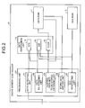
- FIG. 2 is a block diagram of the structure of the cache memory controlling unit according to the first embodiment.
- a cache memory controlling unit 10 includes a DATA-RAM 11, an ECC-RAM 12, a data maintaining unit 13, and a processing unit 20.
- the DATA-RAM 11 is a cache memory storing therein a plurality of pieces of data in a unit of 8 bytes. More specifically, the DATA-RAM 11 is caused to store data output from the execution unit by way of the instruction processing unit, or to serve the data for reads by the instruction processing unit.
- the ECC-RAM 11 is a memory for storing therein ECC data generated by an ECC generating unit 25 that is to be described later. More specifically, the ECC-RAM 12 stores therein 1-byte ECC data generated by the ECC generating unit 25 correspondingly to each piece of data stored in the DATA-RAM 11.
- the data maintaining unit 13 is a buffer that temporarily stores therein the store data received from the execution unit to enable the processing unit 20 to be described later to perform various processes thereto.
- the data maintaining unit 13 includes an STB 14, a WB 15, and an FCDR 16.
- the STB 14 is a buffer that temporarily stores therein the store data received from the execution unit.
- the execution unit transmits store data and the instruction processing unit outputs store-related information such as a store address, a store data width, and aligning information together with a store instruction
- the STB 14 stores therein data-to-be-stored (store byte mark (STBM)) and a store address (ADRS), each detected (generated) and stored by a data detecting unit 21 to be described later, as depicted in FIG. 3 .
- the STBM indicates which bytes of store data are to be stored, and the store address indicates where in the DATA-RAM the data is to be stored.
- FIG. 3 is a schematic of an example of a structure of the information stored in the STB.
- the WB 15 When the data-area-to-be-stored, the area-not-to-be-stored, and the store address are detected before storing the store data taken out from the STB 14 in the DATA-RAM 11, the WB 15 maintains the store data output from the STB 14. For example, as depicted in FIG. 4 , in the same manner as in the STB 14, the WB 15 maintains the data-to-be-stored (store byte mark (STBM)) and a store address (ADRS), associated with each of EVEN and ODD, as depicted in FIG. 4.
- STBM store byte mark
- ADRS store address
- FIG. 4 is a schematic of an example of a structure of the information stored in the WB.
- the FCDR 16 is a buffer that temporarily stores therein the data written in and output from the area-not-to-be-stored in the DATA-RAM 11, as existing data-not-to-be-stored. More specifically, the FCDR 16 stores therein data read by an existing data-not-to-be-stored obtaining unit 23 from the address in the DATA-RAM 11 where existing data-not-to-be-stored, written in an area-not-to-be-stored that is not to be stored, from the store data detected by the data detecting unit 21, is stored. For example, the FCDR 16 maintains existing data-not-to-be-stored, read from the DATA-RAM 11, in an 8-byte area as depicted in FIG. 5 .
- FIG. 5 is a schematic of an example of a structure of information stored in the FCDR.
- the processing unit 20 is a processing unit that executes various processes. Especially in a close relationship with the embodiment, the processing unit 20 includes the data detecting unit 21, a data determining unit 22, the existing data-not-to-be-stored obtaining unit 23, a store data writing unit 24, and the ECC generating unit 25.
- the data detecting unit 21 Upon receiving store data from the execution unit, the data detecting unit 21 detects therein the address in the cache memory into which the store data is stored; the area-to-be-stored where the store data is to be stored; and the area-not-to-be-stored that is not to be stored, from the store data. More specifically, upon receiving an 8-byte store data from the execution unit, the data detecting unit 21 stores the data-to-be-stored (store byte mark (STBM)) and a store address (ADRS) detected from the store data in the STB 14. The data detecting unit 21 also detects an area-not-to-be-stored that is not to be stored from the store data, and transmits the store data to the WB 15.
- STBM store byte mark
- ADRS store address
- the data determining unit 22 determines if any other data written in the address in the cache memory detected by the data detecting unit 21 is present. To explain with a specific example, the data determining unit 22 refers to the address "ADRS" in the DATA-RAM 11, the address detected and stored in the STB 14 by the data detecting unit 21, and determines if other data is already written therein. The result of the determination is notified to the existing data-not-to-be-stored obtaining unit 23 to be described later.
- the existing data-not-to-be-stored obtaining unit 23 obtains the data written in the area-not-to-be-stored, detected by the data detecting unit 21, out of the data written in the address, as existing data-not-to-be-stored.
- the existing data-not-to-be-stored obtaining unit 23 when the existing data-not-to-be-stored obtaining unit 23 is notified from the data determining unit 22 that other data is present in the address "ADRS (e.g., address A)" in the DATA-RAM 11, that is, if a cache hit occurs, the existing data-not-to-be-stored obtaining unit 23 obtains the data written in the detected area-not-to-be-stored (2 bytes), out of the data written in the address, and stores the data in the FCDR 16 as existing data-not-to-be-stored (in this example, the 2-byte data).
- ADRS e.g., address A
- the existing data-not-to-be-stored obtaining unit 23 obtains the data written in the detected area-not-to-be-stored (2 bytes), out of the data written in the address, and stores the data in the FCDR 16 as existing data-not-to-be-stored (in this example, the 2-byte data).
- the store data writing unit 24 merges the existing data-not-to-be-stored obtained by the existing data-not-to-be-stored obtaining unit 23 with the data-to-be-stored in the area-to-be-stored detected by the data detecting unit 21 to generate new store data.
- the store data writing unit 24 then writes the new store data into the address in the cache memory detected by the data detecting unit 21.
- the store data writing unit 24 merges the "2-byte" existing data-not-to-be-stored stored in the FCDR 16 with the "6-byte” data-to-be-stored in the area-to-be-stored and stored in the WB 15, in the WB 15 (e.g., processes these pieces of data with an EOR circuit) to generate new "8-byte” store data.
- the store data writing unit 24 then stores the new store data in the WB 15.
- the store data writing unit 24 then reads the new "8-byte” store data from the WB 15, and writes the data into the detected address "ADRD (e.g., address A)" in the DATA-RAM 11.
- ADRD e.g., address A
- the ECC generating unit 25 generates an ECC for the new store data written in the cache memory by the store data writing unit 24, from the new store data generated by the store data writing unit 24. To explain more specifically with reference to the example, the ECC generating unit 25 reads the new "8-byte" store data generated by the store data writing unit 24 and stored in the WB 15, generates a 1-byte ECC for the new store data written in the DATA-RAM, and stores the ECC to the ECC-RAM 12.
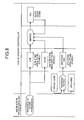
- FIG. 6 is a flowchart of the process performed by the cache memory controlling unit according to the first embodiment.
- the data detecting unit 21 included in the cache memory controlling unit 10 stores the data-to-be-stored (store byte mark (STBM)) and the store address(ADRS) into the STB 14, detects the area-not-to-be-stored that is not to be stored, from the store data, and transmits the store data to the WB 15 (Step S602).
- STBM store byte mark
- ADRS store address
- the data determining unit 22 then refers to the address "ADRS" in the DATA-RAM 11, such an address detected by the data detecting unit 21 and maintained in the STB 14, and determines if any other data is already written therein. In other words, the data determining unit 22 retrieves the cache (Step S603).
- the existing data-not-to-be-stored obtaining unit 23 obtains the data written in the area-not-to-be-stored, out of the data written in the address, from the DATA-RAM 11 as existing data-not-to-be-stored, and stores the obtained existing data-not-to-be-stored in the FCDR 16 (Step S605).
- the store data writing unit 24 then reads the existing data-not-to-be-stored stored in the FCDR 16 into the WB 15, merges the data with the data-to-be-stored, which is in the area to be stored maintained in the WB 15, in the WB 15 to generate new store data, and writes the new store data to the detected address in the DATA-RAM 11 (Step S606).
- the ECC generating unit 25 generates an ECC for the new store data that is written in the DATA-RAM 11 by the store data writing unit 24, from the new store data generated by the store data writing unit 24.
- the ECC generating unit 25 then stores the ECC in the ECC-RAM 12 (Step S607).
- Step S604 if no data-to-be-stored is written (a cache miss occurs) (NO at Step S604), the data that is the store data to be written is registered (Step S608), and the cache is retrieved again (Step S603).
- the cache memory controller upon receiving store data from an execution unit, detects a write address in the cache memory where the store data is to be stored, a store area that is to be stored, and an area-not-to-be-stored that is not to be stored, from the store data; determines if any data-to-be-stored stored previously in the detected write address is present; obtains the data written in the detected area-not-to-be-stored, out of the data written in the write address, as existing data-not-to-be-stored, if it is determined that the data-to be-stored is stored in the write address; merges the obtained existing data-not-to-be-stored with the data-to-be-stored in the detected area-to-be-stored to generate new store data, and writes the new store data to the detected write address; and generates an ECC for the new store data written in the cache memory, based on the generated new store data. Therefore, it is possible to prevent SSI from occurring even
- the cache memory controller generates new store data, as well as an ECC, using the data itself stored in the DATA-RAM, instead of an ECC generated based on the data stored previously. Therefore, the cache memory controller can perform the process without waiting for an ECC to be generated for preceding data. As a result, it is possible to prevent SSI from occurring even when equal to or less than 8-byte data is stored consecutively to the same address, and to generate a correct ECC. Moreover, a 1-bit error can be completely remedied in the RAM.
- the cache memory controller brings the data stored in the area-not-to-be-stored in the DATA-RAM to the FCDR or the WB before executing the store, and merges the store data with the data contained in the area-not-to-be-stored to generate new store data and an ECC; however, the present embodiment is not limited thereto.
- the cache memory controller can also generate new store data and an ECC taking the area-to-be-stored of the preceding store data into consideration in advance.
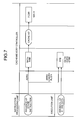
- FIG. 7 is a schematic of movement of data in the IU-REQ process.
- the instruction processing unit transmits (issues) a store instruction that is accompanied by store-related store information such as a store address, a store data width, and aligning information to the cache memory controlling unit.
- store-related store information such as a store address, a store data width, and aligning information
- the cache memory controlling unit Upon receiving the issued store instruction, the cache memory controlling unit generates STBM from the information, and stores the information into the STB together with the ADRS.
- the cache memory controlling unit then inputs the store instruction to a pipeline, and checks if the cache line to be stored is in the cache memory (DATA-RAM).
- the cache memory controlling unit reads the data from the 8-byte data cache memory using the store address, and checks the data for an error. If a cache hit occurs, the cache memory controlling unit sets the read data in the area-to-be-stored to the FCDR. If a cache miss occurs, the cache memory controlling unit requests the data from the main memory.
- FIG. 8 is a schematic of movement of data in the WB-GO process.
- the cache memory controlling unit when the cache memory controlling unit receives a store permission from the instruction processing unit, and if the STB that is to be processed has the highest priority and there is an space in the WB, the cache memory controlling unit issues a WB-GO (write request). In response, the cache memory controlling unit reads the data in the area-to-be-stored from the STB, and data in the area-not-to-be-stored from the FCDR, respectively, and updates the WB with the data. The cache memory controlling unit determines the area-to-be-stored based on the STB-STBM.
- the cache memory controlling unit performs an address match between a WB-GO-ADRS of the current store data-to-be-stored (STB-ADRS that is to be processed by WB-GO) and the ST2-ADRS (address in the ST2-REQ) of the preceding store data that is the store data transmitted from the execution unit prior to the current store data. If the ST2-REQ is at the same timing as the WB-GO, the cache memory controlling unit refers to the ST2-STBM, merges the ST2-DATA additionally, and writes the data into the WB.
- the cache memory controlling unit obtains the data-to-be-stored of the preceding data from the WB, and merges the current data-to-be-stored and the existing data-not-to-be-stored obtained from the FCDR with the data-to-be-stored of the preceding store data, and writes the data into the WB.
- FIG. 9 is a schematic of movement of data in the ST1-REQ process.
- the cache memory controlling unit initiates the ST1-REQ from the WB. In response, the cache memory controlling unit retrieves the cache memory using the WB-ADRS. If a cache hit occurs and no error is present in the DATA-RAM, the cache memory controlling unit writes only the data in the area-not-to-be-stored into the WB using the WB-STBM. If a cache miss occurs, the cache memory controlling unit requests the data from the main memory.
- FIG. 10 is a schematic of movement of data in the ST2-REQ process.
- the cache memory controlling unit initiates the ST2-REQ from the WB.
- the cache memory controlling unit takes out the store data from the WB requested by the ST2-REQ, and updates the DATA-RAM with the data.
- the cache memory controlling unit then generates a 1-byte ECC corresponding to 8-byte data based on this data, and writes the ECC to the ECC-RAM.
- the cache memory controlling unit reflects the data onto the target FCDR. At this time, the cache memory controlling unit updates only the area-to-be-stored using the ST2-STBM. Furthermore, if the addresses of the ST2-ADRS and another WB-ADRS (a WB address excluding the one onto which the ST2 is executed) match, the cache memory controlling unit reflects the store data onto the target WB. In this situation as well, the cache memory controlling unit updates only the area-to-be-stored using the ST2-STBM.
- the cache memory controlling unit cannot reflect the prior store data onto the WB to which the next storing is executed. Therefore, if the ST2-ADRS that is an address of a store preceding by 1 ⁇ makes a match with the ST2-ADR before generation of an ECC, the store data is merged with the data preceding by 1 ⁇ .
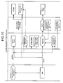
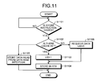
- FIG. 11 is a flowchart of the IU-REQ process.
- the cache memory controlling unit determines if the data-to-be-stored is stored in the DATA-RAM (retrieves the cache) (Step S1102).
- the cache memory controlling unit updates the "LID" to "1" (Step S1103), generates STBM from the received store data, and stores the STBM into the STB together with the ADRS (Step S1104).
- the cache memory controlling unit reads the data-to-be-stored making a cache hit from the DATA-RAM, and stores the data into the FCDR (Step S1105).
- the cache memory controlling unit updates the "LID" to "0", generates STBM from the received store data, and stores the STBM into the STB together with the ADRS (Step S1106).
- FIG. 12 is a flowchart of the WB-GO process.
- the cache memory controlling unit upon receiving a store permission from the instruction processing unit (YES at Step S1201), issues a WB-GO request, and executes the WB-GO process (Step S1202).
- the cache memory controlling unit merges the following data, that is: the data-to-be-stored, in the area-to-be-stored, obtained from the STB; the existing data-not-to-be-stored that is the data in the area-not-to-be-stored and obtained from the FCDR; the data-to-be-stored obtained from another WB when the address in the WB-GO and the address in the ST2 (the data-to-be-stored in the preceding store data) match; and the data-to-be-stored obtained from the same WB when the address in the WB-GO and the address in the same WB (the data-to-be-stored in the preceding store data) match (Step S1203 to Step S1208).
- the cache memory controlling unit then stores the merged data in the WB (Step S1209).
- FIG. 13 is a flowchart of the ST1-REQ process.
- the cache memory controlling unit checks the status of the WB (Step S1302).
- the cache memory controlling unit initiates an ST1-REQ (Step S1304).
- the cache memory controlling unit retrieves the cache again for the store data received from the execution unit (Step S1305). If a cache hit occurs (YES at Step S1305), the cache memory controlling unit updates the LID to "1", reads the data-to-be-stored that made the cache hit from the DATA-RAM, and stores the data in the WB (Step S1306) .
- Step S1305 if a cache hit does not occur (NO at Step S1305), the cache memory controlling unit requests the received store data to the main memory (Step S1308), writes the data into the DATA-RAM (Step S1309), and performs Step S1302 and the steps thereafter.
- Step S1303 if the LID in the WB is not "0" (NO at Step S1303), the cache memory controlling unit initiates an ST2-REQ (Step S1307).
- FIG. 14 is a flowchart of the ST2-REQ process.
- the cache memory controlling unit checks the status of the WB (Step S1401), and if the LID is "1" (YES at Step S1402), the ST2-REQ is initiated (Step S1403).
- the cache memory controlling unit stores the store data from the WB into the DATA-RAM (Step S1404).
- the cache memory controlling unit stores the data in the area-to-be-stored into another WB (Step S1406).
- the cache memory controlling unit stores the data in the area-to-be-stored into the FCDR (Step S1408).
- the cache memory controlling unit stores the data in the area-to-be-stored in that WB (Step S1410). If the address in the ST2 preceding by 1 ⁇ makes a match with the address in the ST2 (YES at Step S1411), the cache memory controlling unit merges the data preceding by 1 ⁇ into the current store data (Step S1412), generates an ECC based on the merged data, and stores the ECC in the ECC-RAM (Step S413).
- Step S1414 if the LID is not "1" (NO Step S1402), a calculator initiates the ST1-REQ (Step S1414).
- the cache memory controlling unit registers the data-to-be-stored, and then detects any data-already-stored stored in the detected address of the cache memory; if the cache memory controlling unit detects the data-already-stored stored in the detected address of the cache memory, the cache memory controlling unit merges new store data with the data-already-stored to further generate new store data, and writes the new store data in the write address detected by the data detecting unit; and the cache memory controlling unit generates an ECC for the new store data that is written in the cache memory based on the generated new store data. Therefore, even when a cache miss occurs, a correct ECC can be generated.
- the cache memory controlling unit when the execution unit transmits store data, the cache memory controlling unit detects a write address in the cache memory into which preceding data, transmitted from the execution unit prior to the store data, is stored, and a preceding area-to-be-stored that is to be stored from the preceding store data; the cache memory controlling unit further determines if the write address of the detected store data makes a match with the write address of the preceding store data; if it is determined that the write address of the store data makes a match with the write address of the preceding store data, the cache memory controlling unit merges the existing data-not-to-be-stored and the data-to-be-stored with the preceding data-to-be-stored in the detected preceding area-to-be-stored to generate new store data, writes the new store data into the write address in the cache memory, and generates an ECC for the new store data written into the cache memory based on the generated new store data.
- the cache memory controlling unit can generate new store data and an ECC taking preceding store data into consideration.
- SSI can be prevented from occurring more reliably even when equal to or less than 8-byte data is stored consecutively to the same address, and a correct ECC can be generated more surely.
- the second embodiment explained the scenario where current store data is merged with, for example, preceding store data, or store data stored in the WB into which the current store data is to be stored to generate new store data.
- current store data is merged with, for example, preceding store data, or store data stored in the WB into which the current store data is to be stored to generate new store data.
- data is to be prioritized in a merger operation.
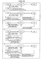
- FIG. 15 is a schematic of an example of a merger of store data. "WB0" and “WB1" depicted in FIG. 15 indicate that these are physically different write buffers.
- the cache memory controlling unit merges the data-to-be-stored in the store data transmitted from the execution unit with existing data-not-to-be-stored that is the data stored in the DATA-RAM corresponding to the area-not-to-be-stored (see (1) in FIG. 15 ).
- the cache memory controlling unit merges the data-to-be-stored of the store data transmitted from the execution unit with existing data-not-to-be-stored that is the data stored in the DATA-RAM corresponding to the area-not-to-be-stored and the data-to-be-stored in the preceding store data (see (2) in FIG. 15 ).
- the cache memory controlling unit merges the data-to-be-stored in the store data stored in the WB0 with the data-to-be-stored in the store data stored in the WB1 (see (3) in FIG. 15 ).
- the cache memory controlling unit merges data-to-be-stored in the store data transmitted from the execution unit with the existing data-not-to-be-stored that is the data stored in the DATA-RAM corresponding to the area-not-to-be-stored, and the data-to-be-stored in the store data stored in the WB0, and stores the merged data in the WB1 (see (4) in FIG. 15 ).
- the cache memory controlling unit merges the data-to-be-stored in the newly generated store data with the data-to-be-stored stored in the WB1 to store the new store data in the WB1 (see (5) in FIG. 15 ).
- FIG. 16 is a schematic of an example of an order of data priority in a data merger.
- the data transmitted by the execution unit is merged with all of the data, including data stored in the DATA-RAM, data found in a retrieval performed after a cache miss, and preceding data; however, the present invention is not limited thereto, and the data to be merged may be selected in any way, e.g., only some of these pieces of data may be merged.
- the whole or a part of the processing described in the embodiments to be automatically executed may be manually executed.
- the processing procedure, the control procedure, the specific names, information containing various kinds of data and parameters may be changed in any way except where specified otherwise.
- each of the elements provided in each of the apparatus depicted in the drawings only represents conceptualized functions thereof, and does not necessary have to be structured physically as depicted in the drawings.
- a specific distributive or integrative structure of each of the apparatus is not limited to that depicted in the drawings, and whole or any part of thereof may be distributed or integrated functionally or physically in any unit depending on various types of loads or usage (for example, the data detecting unit and the data determining unit may be integrated).
- the cache controller, the cache controlling method, and the cache controlling program according to the present invention are useful for writing store data transmitted from the execution unit into a cache memory, as well as generating an ECC for the store data, and particularly suited for preventing SSI from occurring, and for generating a correct ECC, even when equal to or less than 8-byte data is stored consecutively to the same address.
Landscapes
- Engineering & Computer Science (AREA)
- Theoretical Computer Science (AREA)
- Physics & Mathematics (AREA)
- General Engineering & Computer Science (AREA)
- General Physics & Mathematics (AREA)
- Quality & Reliability (AREA)
- Techniques For Improving Reliability Of Storages (AREA)
- Memory System Of A Hierarchy Structure (AREA)
Abstract
Description
- The present invention relates to a cache controller, a cache controlling method, and a cache controlling program that perform a write operation to store data received from an execution unit, and generate an ECC for the store data.
- Conventionally, a data cache memory (DATA-RAM) protects data by appending an Error-Check-and-Correction (ECC) byte to an 8-byte data. An ECC is stored in an ECC cache memory (ECC-RAM) that is separate from DATA-RAM, and dedicatedly provided for ECCs. The ECC-RAM is updated when a register or a write operation is performed to the cache memory.
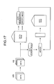
- A common method of generating an ECC will now be explained with reference to
FIG. 17 . As depictedFIG. 17 , to write data into a cache memory, an instruction processor issues a store instruction to a memory processor. Upon receiving the instruction, the memory processor checks if the cache line to be stored is in the cache memory, and at the same time, reads the data in the cache line to be stored from the cache memory and checks the data for an error. At this time, store data issued from an execution unit and alike is written in a store buffer (STB). - When the instruction processor issues a store permission subsequently, the memory processor writes the data taken out from the store buffer into a write buffer (WB), and further writes the data taken out from the write buffer into the DATA-RAM. At the same time as writing the data, the memory processor generates an ECC based on 8-byte fetched data read from the DATA-RAM, using bytes-not-to-be-stored included therein (ECC generation 1). In addition, the memory processor generates an ECC based on data in the bytes-to-be-stored included in the 8-byte store data (ECC generation 2). The memory processor then merges these two ECCs to generate an ECC corresponding to the updated store data, and stores the generated ECC in the ECC-RAM.
- However, a 1-bit error might be different in each of these scenarios, that is, in the data read from the DATA-RAM upon checking for an error when the retrieval access is made to the cache memory in response to the store request; and in the data read therefrom upon generating the ECC after the storing is permitted, and the cache memory is accessed for the write. In other words, if no error is detected at the error check performed upon the data retrieval, but an error is found in the data read upon execution of the write, the ECC corresponding to the data after the write cannot be generated properly. Furthermore, the ECC remaining at this point is one corresponding to the data before the write, and the data before the write has been already lost. Therefore, it is impossible to correct the faulty bit, further making it impossible to correct the 1-bit error upon reading the data before executing the write. The reason why such an uncorrectable error occurs is that, because the data is read from the DATA-RAM twice, the result of each of the reads might be different.
- In response to such an issue, a disclosed technique executes an error check and an ECC generation based on a single read (see
FIG. 18 ). In other words, the disclosed memory processor does not use the data read from DATA-RAM upon executing the write. More specifically, an ECC is generated based on the data stored previously, and the ECC is appended to the store data written in the STB, to generate new store data (seePatent Documents 1 to 4). -
- Patent Document 1: Japanese Laid-open Patent Publication No.
01-185753 - Patent Document 1: Japanese Laid-open Patent Publication No.
03-108041 - Patent Document 1: Japanese Laid-open Patent Publication No.
10-232789 - Patent Document 1: Japanese Laid-open Patent Publication No.
2004-514184 - However, these conventional techniques have a problem that, when data of equal to or less than 8 bytes are stored in the same address consecutively, Store-Store-Interlock (SSI) may occur, resulting in performance deterioration. More specifically, because a memory processor with such a structure maintains data-not-to-be-stored as an ECC, if the next store instruction executes a write in the same area as the preceding store instruction, the memory processor has to wait for the preceding storing to complete before generating an ECC. Therefore, the memory processor results in detecting SSI for store data other than 8-byte full-store data, thus fails to execute the next storing.
- Therefore, the present invention is made to solve the problems of the conventional techniques. An object of the present invention is to provide a cache controller, a cache controlling method, and a cache controlling program that are capable of preventing SSI from occurring even when equal to or less than 8-byte data is stored consecutively to the same address, and capable of generating a correct ECC.
- To solve the problems described above and achieve the object, the invention set forth in
claim 1 is a cache memory controller for writing store data received from an execution unit into a cache memory and generating an ECC for the store data. The cache memory controller includes a data detecting unit that detects a write address in the cache memory into which the store data is stored, an area-to-be-stored of the store data that is to be stored and an area-not-to-be-stored that is not to be stored, when the store data is transmitted from the execution unit; a data determining unit that determines whether data-to-be-stored that is already written is present in the write address detected by the data detecting unit; an existing data-not-to-be-stored obtaining unit that obtains, from the data written in the write address, data detected by the data detecting unit and written in the area-not-to-be-stored, as existing data-not-to-be-stored, when the data determining unit determines that the data-to-be-stored is present in the write address; a store data writing unit that merges the existing data-not-to-be-stored obtained by the existing data-not-to-be-stored obtaining unit with the data-to-be-stored in the area-to-be-stored detected by the data detecting unit to generate new store data, and writes the new store data into the write address detected by the data detecting unit; and an ECC generating unit that generates an ECC for the new store data written by the store data writing unit into the cache memory, from the new store data generated by the store data writing unit. - The invention set forth in
claim 2 further includes a data re-detecting unit that, when the data determining unit determines that no data-to-be-stored is present in the write address of the cache memory, detects data-already-stored already stored in the address of the cache memory detected by the data detecting unit after registering the data-to-be-stored thereto, wherein when the data re-detecting unit detects the data-already-stored already stored in the write address of the cache memory, the store data writing unit merges the new store data with the data-already-stored to generate further new store data, and writes the further new store data in the write address detected by the data detecting unit, and the ECC generating unit generates an ECC for the further new store data written by the store data writing unit into the cache memory, from the further new store data generated by the store data writing unit. - In the invention set forth in
claim 3, when the store data is transmitted from the execution unit, the data detecting unit further detects a write address of a cache memory into which preceding store data transmitted from the execution unit prior to the store data is to be stored, and a preceding area-to-be-stored that is to be stored in the preceding store data, the data determining unit further determines whether the write address of the store data detected by the data detecting unit makes a match with the write address of the preceding store data, when the data determining unit determines that the write address of the store data makes a match with the write address of the preceding store data, the store data writing unit merges the existing data-not-to-be-stored, the data-to-be-stored, and the preceding data-to-be-stored in the preceding area-to-be-stored detected by the data detecting unit to generate new store data, and writes the new store data into the write address in the cache memory, and the ECC generating unit generates an ECC for new data written by the store data writing unit into the cache memory, from the new store data generated by the store data writing unit. - The invention set forth in
claim 4 is a cache memory controlling method suitable for writing store data received from an execution unit into a cache memory and generating an ECC for the store data. The cache memory controlling method includes a data detecting step of detecting a write address in the cache memory into which the store data is stored, an area-to-be-stored of the store data that is to be stored and an area-not-to-be-stored that is not to be stored, when the store data is transmitted from the execution unit; a data determining step of determining whether data-to-be-stored that is already written is present in the write address detected at the data detecting step; an existing data-not-to-be-stored obtaining step of obtaining, from the data written in the write address, data detected at the data detecting step and written in the area-not-to-be-stored, as existing data-not-to-be-stored, when it is determined that the data-to-be-stored is present in the write address at the data determining step; a store data writing step of merging the existing data-not-to-be-stored obtained at the existing data-not-to-be-stored obtaining step with the data-to-be-stored in the area-to-be-stored detected at the data detecting step to generate new store data, and writing the new store data into the write address detected at the data detecting step; and an ECC generating step of generating an ECC for the new store data written at the store data writing step into the cache memory, from the new store data generated at the store data writing step. - The invention set forth in
claim 5 further includes a data re-detecting step of, when it is determined that no data-to-be-stored is present in the write address of the cache memory at the data determining step, detecting data-already-stored already stored in the address of the cache memory detected at the data detecting step after registering the data-to-be-stored thereto, wherein the store data writing step, when the data-already-stored already stored in the write address of the cache memory is detected, includes merging the new store data with the data-already-stored to generate further new store data, and writing the further new store data in the write address detected at the data detecting step, and the ECC generating step includes generating an ECC for the further new store data written at the store data writing step into the cache memory, from the further new store data generated at the store data writing step. - In the invention set forth in claim 6, the data detecting step, when the store data is transmitted from the execution unit, includes further detecting a write address of a cache memory into which preceding store data transmitted from the execution unit prior to the store data is to be stored, and a preceding area-to-be-stored that is to be stored in the preceding store data, the data determining step includes further determining whether the write address of the store data detected at the data detecting step makes a match with the write address of the preceding store data, the store data writing step, when it is determined that the write address of the store data makes a match with the write address of the preceding store data at the data determining step, includes merging the existing data-not-to-be-stored, the data-to-be-stored, and the preceding data-to-be-stored in the preceding area-to-be-stored detected at the data detecting step to generate new store data, and writing the new store data into the write address in the cache memory, and the ECC generating step includes generating an ECC for new data written at the store data writing step into the cache memory, from the new store data generated at the store data writing step.
- The invention set forth in claim 7 is a cache memory controlling program that causes a computer to write store data received from an execution unit into a cache memory and generate an ECC for the store data. The cache memory controlling program includes a data detecting step of detecting a write address in the cache memory into which the store data is stored, an area-to-be-stored of the store data that is to be stored and an area-not-to-be-stored that is not to be stored, when the store data is transmitted from the execution unit; a data determining step of determining whether data-to-be-stored that is already written is present in the write address detected at the data detecting step; an existing data-not-to-be-stored obtaining step of obtaining, from the data written in the write address, data detected at the data detecting step and written in the area-not-to-be-stored, as existing data-not-to-be-stored, when it is determined that the data-to-be-stored is present in the write address at the data determining step; a store data writing step of merging the existing data-not-to-be-stored obtained at the existing data-not-to-be-stored obtaining step with the data-to-be-stored in the area-to-be-stored detected at the data detecting step to generate new store data, and writing the new store data into the write address detected at the data detecting step; and an ECC generating step of generating an ECC for the new store data written at the store data writing step into the cache memory, from the new store data generated at the store data writing step.
- The invention set forth in
claim 8 further includes a data re-detecting step of, when it is determined that no data-to-be-stored is present in the write address of the cache memory at the data determining step, detecting data-already-stored already stored in the address of the cache memory detected at the data detecting step after registering the data-to-be-stored thereto after registering the data-to-be-stored thereto, wherein the store data writing step, when the data-already-stored already stored in the write address of the cache memory is detected, includes merging the new store data with the data-already-stored to generate further new store data, and writing the further new store data in the write address detected at the data detecting step, and the ECC generating step includes generating an ECC for the further new store data written at the store data writing step into the cache memory, from the further new store data generated at the store data writing step. - In the invention set forth in claim 9, the data detecting step, when the store data is transmitted from the execution unit, includes further detecting a write address of a cache memory into which preceding store data transmitted from the execution unit prior to the store data is to be stored, and a preceding area-to-be-stored that is to be stored in the preceding store data, the data determining step includes further determining whether the write address of the store data detected at the data detecting step makes a match with the write address of the preceding store data, the store data writing step, when it is determined that the write address of the store data makes a match with the write address of the preceding store data at the data determining step, includes merging the existing data-not-to-be-stored, the data-to-be-stored, and the preceding data-to-be-stored in the preceding area-to-be-stored detected at the data detecting step to generate new store data, and writing the new store data into the write address in the cache memory, and the ECC generating step includes generating an ECC for new data written at the store data writing step into the cache memory, from the new store data generated at the store data writing step.
- According to the present invention, upon receiving store data from the execution unit, the data detecting unit detects a write address in a cache memory into which the store data is stored, an area-to-be-stored that is to be stored in the store data, and an area-not-to-be-stored that is not to be stored from the store data; the data determining unit determines whether any data-to-be-stored is already written in the detected write address; when the data determining unit determines that the data-to-be-stored is present in the write address, the existing data-not-to-be-stored obtaining unit obtains data written in the detected area-not-to-be-stored from the data written in the write address as existing data-not-to-be-stored; the store data writing unit merges the obtained existing data-not-to-be-stored with the data-to-be-stored in the detected area-to-be-stored to generate new store data, and writes the new store data in the detected write address; and the ECC generating unit generates an ECC for the new store data written in the cache memory based on the generated new store data. Therefore, it is possible to prevent SSI from occurring even when equal to or less than 8-byte data is stored consecutively to the same address, as well as generating a correct ECC.
- Furthermore, according to the present invention, when the data determining unit determines that no data-to-be-stored is present in the write address in the cache memory, after the data-to-be-stored is registered thereto, the data re-detecting unit detects data-already-stored already stored in the detected address of the cache memory; when the data re-detecting unit detects the data-already-stored already stored in the write address in the cache memory, the store data writing unit merges the new store data with the data-already-stored to generate further new store data, and writes the further new store data in the write address detected by the data detecting unit; and the ECC generating unit generates an ECC for further new store data written in the cache memory, based the generated further new store data. Therefore, a correct ECC can be generated even when a cache miss occurs.
- Furthermore, according to the present invention, upon receiving store data from the execution unit, the data detecting unit further detects a write address in a cache memory in which preceding store data received from the execution unit prior to the store data is to be stored, and a preceding area-to-be-stored that is to be stored in the preceding store data; the data determining unit further determines whether the detected write address for the store data makes a match with the write address for the preceding store data; when the data determining unit determines that the write address for the store data makes a match with the write address for the preceding store data, the store data writing unit merges the existing data-not-to-be-stored with the data-to-be-stored and the preceding data-to-be-stored in the detected preceding area-to-be-stored to generate new store data, and writes the new store data in the write address in the cache memory; and the ECC generating unit generates an ECC for the new data written in the cache memory, based on the generated new store data. Therefore, the cache memory controlling unit can generate new store data and an ECC taking preceding store data into consideration. As a result, SSI can be prevented from occurring more reliably even when equal to or less than 8-byte data is stored consecutively to the same address, and a correct ECC can be generated more surely.
-
FIG. 1 is a schematic of a system structure depicting an entire structure of a cache memory controller according to a first embodiment of the present invention. -
FIG. 2 is a block diagram of a structure of a cache memory controlling unit according to the first embodiment. -
FIG. 3 is a schematic of an example of a structure of information stored in an STB. -
FIG. 4 is a schematic of an example of a structure of information stored in a WB. -
FIG. 5 is a schematic of an example of a structure of information stored in an FCDR. -
FIG. 6 is a flowchart of a process performed by the cache memory controlling unit according to the first embodiment. -
FIG. 7 is a schematic of movement of data in an IU-REQ process. -
FIG. 8 is a schematic of movement of data in a WB-GO process. -
FIG. 9 is a schematic of movement of data in an ST1-REQ process. -
FIG. 10 is a schematic of movement of data in an ST2-REQ process. -
FIG. 11 is a flowchart of the IU-REQ process. -
FIG. 12 is a flowchart of the WB-GO process. -
FIG. 13 is a flowchart of the ST1-REQ process. -
FIG. 14 is a flowchart of the ST2-REQ process. -
FIG. 15 is a schematic of examples of store data merger. -
FIG. 16 is a schematic of an example of an order of data priority in a data merger. -
FIG. 17 is a schematic for explaining a conventional technology. -
FIG. 18 is another schematic for explaining a conventional technology. -
- 10
- Cache memory controlling unit
- 11
- DATA-RAM
- 12
- ECC-RAM
- 13
- Data maintaining unit
- 14
- STB
- 15
- WB
- 16
- FCDR
- 20
- Processing unit
- 21
- Data detecting unit
- 22
- Data determining unit
- 23
- Existing data-not-to-be-stored obtaining unit
- 24
- Store data writing unit
- 25
- ECC generating unit
- Exemplary embodiments of a cache controller, a cache controlling method, and a cache controlling program according to embodiments of the present invention will now be explained in detail with reference to the appended drawings. The explanations will be given in order of the overview and characteristics of a cache controlling unit according to the embodiments, and the structure of and processes performed by the cache controlling unit. Various variations of the embodiments will be explained last.
- To begin with, an overview and a characteristic of a cache memory controller according to an embodiment of the present invention will be explained with reference to
FIG. 1. FIG. 1 is a schematic of a system structure depicting an entire structure of the cache memory controller according to a first embodiment of the present invention. - As depicted in
FIG. 1 , this cache memory controller is connected to an execution unit and an instruction processing unit to realize a central processing unit (CPU or MPU). The central processing unit is connected to a memory controlling unit that reads or writes data from or to a main memory. The instruction processing unit connected to a cache memory controlling unit transmits a store instruction appended with store-related information such as a store address, a store data width, and aligning information to the cache memory controlling unit. The execution unit transmits 8-byte store data to the cache memory controlling unit. - The cache memory controlling unit includes: a plurality of store buffers (STB) that stores therein 8-byte store data transmitted by the execution unit; a plurality of write buffers (WB) that temporarily maintains the store data to be stored (to be written) in a DATA-RAM; the DATA-RAM that is a cache memory that stores therein 8-byte store data; a plurality of fetch data registers (FCDR) that maintains data output from the DATA-RAM; and an ECC-RAM that stores therein an ECC corresponding to 8-byte store data to be stored in the DATA-RAM.
- Using such a structure, the cache memory controlling unit generally writes store data received from the execution unit onto the cache memory, as well as generating an ECC for the store data. Especially, a main characteristic of the cache memory controlling unit is in its capability of preventing SSI from occurring even when equal to or less than 8-byte data is stored consecutively to the same address, and of generating a correct ECC.
- To explain this main characteristic more specifically, upon receiving store data from the execution unit, the cache memory controlling unit detects therein an address into which the store data is stored; an area-to-be-stored ; and an area-not-to-be-stored that is not to be stored, from the store data (See Step (1) in
FIG. 1 ). To use a specific example, let us assume that the execution unit transmits 8-byte store data having 6-byte data that is to be maintained (to be stored) in the DATA-RAM, and 2-byte data that is not to be maintained (not to be stored). In this scenario, the cache memory controlling unit detects, for example, an "address A" that is an address of the DATA-RAM in which the store data is to be stored; "6 bytes" that is an area-to-be-stored that is to be stored in the store data; and "2 bytes" that is an area-not-to-be-stored that is not to be stored. In addition, the cache memory controlling unit maintains the store data in the STB, and outputs the store data to the WB. - The cache memory controlling unit then determines if any other data written in the detected address of the cache memory is present (see Step (2) in
FIG. 1 ). To explain more specifically with reference to the example, the cache memory controlling unit refers to the detected address "address A" in the DATA-RAM, and determines if other data is already written in the address (retrieves the cache). - If it is determined that other data is present in the address of the cache memory, the cache memory controlling unit obtains the data from the area-not-to-be-stored detected earlier in the data that is stored in the address, as existing data-not-to-be-stored (see Step (3) in
FIG. 1 ). To explain more specifically with reference to the example, if it is determined that other data is present in the address "address A" of the DATA-RAM, that is, if a cache hit occurs, the cache memory controlling unit stores data in the detected "2-byte" area-not-to-be-stored, out of the data stored in the address, as existing data-not-to-be-stored (in this example, 2-byte data) in the FCDR. Alternatively, the FCDR may store the entire "8 bytes" including the "2 bytes", instead of only the "2 bytes" in the area-not-to-be-stored. - The cache memory controlling unit then generates new data-to-be-stored by merging the obtained existing data-not-to-be-stored with the data-to-be-stored detected earlier in the area-to-be-stored, and writes the data in the detected address in the cache memory (see Step (4) in
FIG. 1 ). To explain more specifically with reference to the example, the cache memory controlling unit reads and stores the "2-byte" existing data-not-to-be-stored, obtained and maintained in the FCDR, into the WB; at the same time, the cache memory controlling unit generates new "8-byte" store data by merging this existing data-not-to-be-stored with the "6-byte" data-to-be-stored, and stores the generated new store data in the WB. The cache memory controlling unit then reads the new "8-byte" store data from the WB, and writes the data in the detected address in the DATA-RAM, the address A. - The cache memory controlling unit generates an ECC for the new store data written in the cache memory, based on the generated new store data (see step (5) in
FIG. 1 ). To explain more specifically with reference to the example, the cache memory controlling unit generates a 1-byte ECC for the new store data written in the DATA-RAM from the "8-byte" new store data generated and maintained in the WB, and stores the ECC in the ECC-RAM. - In this manner, before executing the store, the cache memory controlling unit according to the first embodiment brings the data from the area-not-to-be-stored (the data in the area not overwritten by the store data) and maintains the data itself in the WB, instead of the ECC generated from the data stored previously in the DATA-RAM; and merges the data-to-be-stored with the data in the area-not-to-be-stored to generate new store data and an ECC. As a result, as mentioned above as the main characteristic, the main characteristic of the cache memory is in that SSI can be prevented from occurring even when equal to or less than 8-byte data is consecutively stored to the same address, and that a correct ECC can be generated.
- A structure of the cache memory controlling unit depicted in
FIG. 1 will now be explained with reference toFIG. 2. FIG. 2 is a block diagram of the structure of the cache memory controlling unit according to the first embodiment. As depicted inFIG. 2 , a cachememory controlling unit 10 includes a DATA-RAM 11, an ECC-RAM 12, adata maintaining unit 13, and aprocessing unit 20. - The DATA-
RAM 11 is a cache memory storing therein a plurality of pieces of data in a unit of 8 bytes. More specifically, the DATA-RAM 11 is caused to store data output from the execution unit by way of the instruction processing unit, or to serve the data for reads by the instruction processing unit. - The ECC-
RAM 11 is a memory for storing therein ECC data generated by anECC generating unit 25 that is to be described later. More specifically, the ECC-RAM 12 stores therein 1-byte ECC data generated by theECC generating unit 25 correspondingly to each piece of data stored in the DATA-RAM 11. - The
data maintaining unit 13 is a buffer that temporarily stores therein the store data received from the execution unit to enable theprocessing unit 20 to be described later to perform various processes thereto. In a close relationship with the embodiment, thedata maintaining unit 13 includes anSTB 14, aWB 15, and anFCDR 16. - The
STB 14 is a buffer that temporarily stores therein the store data received from the execution unit.
To explain with a specific example, when the execution unit transmits store data and the instruction processing unit outputs store-related information such as a store address, a store data width, and aligning information together with a store instruction, theSTB 14 stores therein data-to-be-stored (store byte mark (STBM)) and a store address (ADRS), each detected (generated) and stored by adata detecting unit 21 to be described later, as depicted inFIG. 3 . The STBM indicates which bytes of store data are to be stored, and the store address indicates where in the DATA-RAM the data is to be stored.FIG. 3 is a schematic of an example of a structure of the information stored in the STB. - When the data-area-to-be-stored, the area-not-to-be-stored, and the store address are detected before storing the store data taken out from the
STB 14 in the DATA-RAM 11, theWB 15 maintains the store data output from theSTB 14. For example, as depicted inFIG. 4 , in the same manner as in theSTB 14, theWB 15 maintains the data-to-be-stored (store byte mark (STBM)) and a store address (ADRS), associated with each of EVEN and ODD, as depicted inFIG. 4. FIG. 4 is a schematic of an example of a structure of the information stored in the WB. - The
FCDR 16 is a buffer that temporarily stores therein the data written in and output from the area-not-to-be-stored in the DATA-RAM 11, as existing data-not-to-be-stored. More specifically, theFCDR 16 stores therein data read by an existing data-not-to-be-stored obtainingunit 23 from the address in the DATA-RAM 11 where existing data-not-to-be-stored, written in an area-not-to-be-stored that is not to be stored, from the store data detected by thedata detecting unit 21, is stored. For example, theFCDR 16 maintains existing data-not-to-be-stored, read from the DATA-RAM 11, in an 8-byte area as depicted inFIG. 5 .
FIG. 5 is a schematic of an example of a structure of information stored in the FCDR. - The
processing unit 20 is a processing unit that executes various processes. Especially in a close relationship with the embodiment, theprocessing unit 20 includes thedata detecting unit 21, adata determining unit 22, the existing data-not-to-be-stored obtainingunit 23, a storedata writing unit 24, and theECC generating unit 25. - Upon receiving store data from the execution unit, the
data detecting unit 21 detects therein the address in the cache memory into which the store data is stored; the area-to-be-stored where the store data is to be stored; and the area-not-to-be-stored that is not to be stored, from the store data. More specifically, upon receiving an 8-byte store data from the execution unit, thedata detecting unit 21 stores the data-to-be-stored (store byte mark (STBM)) and a store address (ADRS) detected from the store data in theSTB 14. Thedata detecting unit 21 also detects an area-not-to-be-stored that is not to be stored from the store data, and transmits the store data to theWB 15. For example, thedata detecting unit 21 causes theSTB 14 to maintain STBM that is the area to be stored (6 bytes), and the store address (ADRS=address A) detected in the store data received from the execution unit. At the same time, thedata detecting unit 21 detects the area-not-to-be-stored that is not to be stored (2 bytes), and transmits the store data to theWB 15. - The
data determining unit 22 determines if any other data written in the address in the cache memory detected by thedata detecting unit 21 is present. To explain with a specific example, thedata determining unit 22 refers to the address "ADRS" in the DATA-RAM 11, the address detected and stored in theSTB 14 by thedata detecting unit 21, and determines if other data is already written therein. The result of the determination is notified to the existing data-not-to-be-stored obtainingunit 23 to be described later. - If the
data determining unit 22 determines that other data written in the address of the cache memory is present, the existing data-not-to-be-stored obtainingunit 23 obtains the data written in the area-not-to-be-stored, detected by thedata detecting unit 21, out of the data written in the address, as existing data-not-to-be-stored. To explain more specifically with reference to the example, when the existing data-not-to-be-stored obtainingunit 23 is notified from thedata determining unit 22 that other data is present in the address "ADRS (e.g., address A)" in the DATA-RAM 11, that is, if a cache hit occurs, the existing data-not-to-be-stored obtainingunit 23 obtains the data written in the detected area-not-to-be-stored (2 bytes), out of the data written in the address, and stores the data in theFCDR 16 as existing data-not-to-be-stored (in this example, the 2-byte data). - The store
data writing unit 24 merges the existing data-not-to-be-stored obtained by the existing data-not-to-be-stored obtainingunit 23 with the data-to-be-stored in the area-to-be-stored detected by thedata detecting unit 21 to generate new store data. The storedata writing unit 24 then writes the new store data into the address in the cache memory detected by thedata detecting unit 21. To explain more specifically with reference to the example, the storedata writing unit 24 merges the "2-byte" existing data-not-to-be-stored stored in theFCDR 16 with the "6-byte" data-to-be-stored in the area-to-be-stored and stored in theWB 15, in the WB 15 (e.g., processes these pieces of data with an EOR circuit) to generate new "8-byte" store data. The storedata writing unit 24 then stores the new store data in theWB 15. The storedata writing unit 24 then reads the new "8-byte" store data from theWB 15, and writes the data into the detected address "ADRD (e.g., address A)" in the DATA-RAM 11. - The
ECC generating unit 25 generates an ECC for the new store data written in the cache memory by the storedata writing unit 24, from the new store data generated by the storedata writing unit 24. To explain more specifically with reference to the example, theECC generating unit 25 reads the new "8-byte" store data generated by the storedata writing unit 24 and stored in theWB 15, generates a 1-byte ECC for the new store data written in the DATA-RAM, and stores the ECC to the ECC-RAM 12. - A process performed by the cache memory controlling unit will now be explained with reference to
FIG. 6. FIG. 6 is a flowchart of the process performed by the cache memory controlling unit according to the first embodiment. - As depicted in
FIG. 6 , if store data is received from the execution unit (YES at Step S601), thedata detecting unit 21 included in the cachememory controlling unit 10 stores the data-to-be-stored (store byte mark (STBM)) and the store address(ADRS) into theSTB 14, detects the area-not-to-be-stored that is not to be stored, from the store data, and transmits the store data to the WB 15 (Step S602). - The
data determining unit 22 then refers to the address "ADRS" in the DATA-RAM 11, such an address detected by thedata detecting unit 21 and maintained in theSTB 14, and determines if any other data is already written therein. In other words, thedata determining unit 22 retrieves the cache (Step S603). - If any other data is already written therein (a cache hit occurs) (YES at Step S604), the existing data-not-to-be-stored obtaining
unit 23 obtains the data written in the area-not-to-be-stored, out of the data written in the address, from the DATA-RAM 11 as existing data-not-to-be-stored, and stores the obtained existing data-not-to-be-stored in the FCDR 16 (Step S605). - The store
data writing unit 24 then reads the existing data-not-to-be-stored stored in theFCDR 16 into theWB 15, merges the data with the data-to-be-stored, which is in the area to be stored maintained in theWB 15, in theWB 15 to generate new store data, and writes the new store data to the detected address in the DATA-RAM 11 (Step S606). - The
ECC generating unit 25 generates an ECC for the new store data that is written in the DATA-RAM 11 by the storedata writing unit 24, from the new store data generated by the storedata writing unit 24. TheECC generating unit 25 then stores the ECC in the ECC-RAM 12 (Step S607). - On the contrary, referring back to Step S604, if no data-to-be-stored is written (a cache miss occurs) (NO at Step S604), the data that is the store data to be written is registered (Step S608), and the cache is retrieved again (Step S603).
- As described above, according to the first embodiment, upon receiving store data from an execution unit, the cache memory controller detects a write address in the cache memory where the store data is to be stored, a store area that is to be stored, and an area-not-to-be-stored that is not to be stored, from the store data; determines if any data-to-be-stored stored previously in the detected write address is present; obtains the data written in the detected area-not-to-be-stored, out of the data written in the write address, as existing data-not-to-be-stored, if it is determined that the data-to be-stored is stored in the write address; merges the obtained existing data-not-to-be-stored with the data-to-be-stored in the detected area-to-be-stored to generate new store data, and writes the new store data to the detected write address; and generates an ECC for the new store data written in the cache memory, based on the generated new store data. Therefore, it is possible to prevent SSI from occurring even when equal to or less than 8-byte data is stored consecutively to the same address, and to generate a correct ECC.
- More specifically, the cache memory controller generates new store data, as well as an ECC, using the data itself stored in the DATA-RAM, instead of an ECC generated based on the data stored previously. Therefore, the cache memory controller can perform the process without waiting for an ECC to be generated for preceding data. As a result, it is possible to prevent SSI from occurring even when equal to or less than 8-byte data is stored consecutively to the same address, and to generate a correct ECC. Moreover, a 1-bit error can be completely remedied in the RAM.
- The cache memory controller according to the first embodiment described above brings the data stored in the area-not-to-be-stored in the DATA-RAM to the FCDR or the WB before executing the store, and merges the store data with the data contained in the area-not-to-be-stored to generate new store data and an ECC; however, the present embodiment is not limited thereto. When the preceding data is stored in the same address, the cache memory controller can also generate new store data and an ECC taking the area-to-be-stored of the preceding store data into consideration in advance.
- Therefore, in a second embodiment of the present invention, explanations will be given in detail how data is moved among the STB, the WB, and the FCDR that are the buffers on which store data is processed, and the DATA-RAM and the ECC-RAM in which store data and ECCs are stored, with reference to
FIGS. 7 to 14 . Furthermore, according to the second embodiment, in a situation where the preceding data is stored in the same address, the cache memory controller generates new store data and an ECC taking the area-to-be-stored of the preceding store data into consideration in advance. - To begin with, an Instruction Unit-Request (IU-REQ) process that is executed upon receiving a store request from the execution unit/the instruction processing unit will be explained with reference to
FIG. 7. FIG. 7 is a schematic of movement of data in the IU-REQ process. - As depicted in
FIG. 7 , the instruction processing unit transmits (issues) a store instruction that is accompanied by store-related store information such as a store address, a store data width, and aligning information to the cache memory controlling unit. Upon receiving the issued store instruction, the cache memory controlling unit generates STBM from the information, and stores the information into the STB together with the ADRS. - The cache memory controlling unit then inputs the store instruction to a pipeline, and checks if the cache line to be stored is in the cache memory (DATA-RAM). The cache memory controlling unit reads the data from the 8-byte data cache memory using the store address, and checks the data for an error. If a cache hit occurs, the cache memory controlling unit sets the read data in the area-to-be-stored to the FCDR. If a cache miss occurs, the cache memory controlling unit requests the data from the main memory.
- A Write-Buffer-GO (WB-GO) process in which store data is written from the STB into the WB will now be explained with reference to
FIG. 8. FIG. 8 is a schematic of movement of data in the WB-GO process. - As depicted in
FIG. 8 , when the cache memory controlling unit receives a store permission from the instruction processing unit, and if the STB that is to be processed has the highest priority and there is an space in the WB, the cache memory controlling unit issues a WB-GO (write request). In response, the cache memory controlling unit reads the data in the area-to-be-stored from the STB, and data in the area-not-to-be-stored from the FCDR, respectively, and updates the WB with the data. The cache memory controlling unit determines the area-to-be-stored based on the STB-STBM. - In addition, the cache memory controlling unit performs an address match between a WB-GO-ADRS of the current store data-to-be-stored (STB-ADRS that is to be processed by WB-GO) and the ST2-ADRS (address in the ST2-REQ) of the preceding store data that is the store data transmitted from the execution unit prior to the current store data. If the ST2-REQ is at the same timing as the WB-GO, the cache memory controlling unit refers to the ST2-STBM, merges the ST2-DATA additionally, and writes the data into the WB. In other words, if a match occurs between the DATA-RAM address in which the preceding store data is to be stored and the DATA-RAM address into which the current store data is to be stored, the cache memory controlling unit obtains the data-to-be-stored of the preceding data from the WB, and merges the current data-to-be-stored and the existing data-not-to-be-stored obtained from the FCDR with the data-to-be-stored of the preceding store data, and writes the data into the WB.
- A Storel-Request (ST1-REQ) process performed when a cache miss occurs in
FIG. 7 will now be explained with reference toFIG. 9. FIG. 9 is a schematic of movement of data in the ST1-REQ process. - As depicted in
FIG. 9 , when the area-to-be-stored is not in the DATA-RAM although the store data has been stored in the WB, the cache memory controlling unit initiates the ST1-REQ from the WB. In response, the cache memory controlling unit retrieves the cache memory using the WB-ADRS. If a cache hit occurs and no error is present in the DATA-RAM, the cache memory controlling unit writes only the data in the area-not-to-be-stored into the WB using the WB-STBM. If a cache miss occurs, the cache memory controlling unit requests the data from the main memory. - A Store2-Request (ST2-REQ) performed upon writing store data from the WB to the cache memory and upon generating an ECC will now be explained with reference to
FIG. 10. FIG. 10 is a schematic of movement of data in the ST2-REQ process. - As depicted in
FIG. 10 , if the area-to-be-stored is present in the cache memory, the cache memory controlling unit initiates the ST2-REQ from the WB. Upon initiating the ST2-REQ, the cache memory controlling unit takes out the store data from the WB requested by the ST2-REQ, and updates the DATA-RAM with the data. The cache memory controlling unit then generates a 1-byte ECC corresponding to 8-byte data based on this data, and writes the ECC to the ECC-RAM. - If the addresses of the ST2-ADRS and the STB-ADRS (an address in each store buffer) match, then the cache memory controlling unit reflects the data onto the target FCDR. At this time, the cache memory controlling unit updates only the area-to-be-stored using the ST2-STBM. Furthermore, if the addresses of the ST2-ADRS and another WB-ADRS (a WB address excluding the one onto which the ST2 is executed) match, the cache memory controlling unit reflects the store data onto the target WB. In this situation as well, the cache memory controlling unit updates only the area-to-be-stored using the ST2-STBM.
- Moreover, when ST2-REQ is generated consecutively, the cache memory controlling unit cannot reflect the prior store data onto the WB to which the next storing is executed. Therefore, if the ST2-ADRS that is an address of a store preceding by 1τ makes a match with the ST2-ADR before generation of an ECC, the store data is merged with the data preceding by 1τ.
- A process flow of each of the processes "store request issued from the execution unit/instruction processing unit (IU-REQ)", "writing from the STB to the WB (WB-GO)", "retrieving cache memory (ST1-REQ)", and "writing into cache memory (ST2-REQ)" will now be explained with reference to
FIGS. 11 to 14 . "LID" mentioned in a flowchart of each of these processes suggests that an area-to-be-stored is exclusively servicing in the cache memory, and the "LID" is updated when a cache hit occurs, and stored in the STB and the WB. - To begin with, the IU-REQ, depicted in
FIG. 7 , will be explained with reference toFIG. 11. FIG. 11 is a flowchart of the IU-REQ process. - As depicted in
FIG. 11 , if the instruction processing unit transmits (issues) a store instruction (YES at Step S1101), the cache memory controlling unit determines if the data-to-be-stored is stored in the DATA-RAM (retrieves the cache) (Step S1102). - If no cache hit occurs (YES at Step S1102), the cache memory controlling unit updates the "LID" to "1" (Step S1103), generates STBM from the received store data, and stores the STBM into the STB together with the ADRS (Step S1104). At the same time, the cache memory controlling unit reads the data-to-be-stored making a cache hit from the DATA-RAM, and stores the data into the FCDR (Step S1105).
- On the contrary, if no cache hit occurs (NO at Step S1102), the cache memory controlling unit updates the "LID" to "0", generates STBM from the received store data, and stores the STBM into the STB together with the ADRS (Step S1106).
- The WB-GO process depicted in
FIG. 8 will now be explained with reference toFIG. 12. FIG. 12 is a flowchart of the WB-GO process. - As depicted in
FIG. 12 , upon receiving a store permission from the instruction processing unit (YES at Step S1201), the cache memory controlling unit issues a WB-GO request, and executes the WB-GO process (Step S1202). - In response, the cache memory controlling unit merges the following data, that is: the data-to-be-stored, in the area-to-be-stored, obtained from the STB; the existing data-not-to-be-stored that is the data in the area-not-to-be-stored and obtained from the FCDR; the data-to-be-stored obtained from another WB when the address in the WB-GO and the address in the ST2 (the data-to-be-stored in the preceding store data) match; and the data-to-be-stored obtained from the same WB when the address in the WB-GO and the address in the same WB (the data-to-be-stored in the preceding store data) match (Step S1203 to Step S1208). The cache memory controlling unit then stores the merged data in the WB (Step S1209).
- The ST1-REQ process depicted in
FIG. 9 will now be explained with reference toFIG. 13. FIG. 13 is a flowchart of the ST1-REQ process. - As depicted in
FIG. 13 , if a cache miss occurs (YES at Step S1301), the cache memory controlling unit checks the status of the WB (Step S1302). - If the LID in the WB is set to "0" (YES at Step S1303), the cache memory controlling unit initiates an ST1-REQ (Step S1304).
- The cache memory controlling unit retrieves the cache again for the store data received from the execution unit (Step S1305). If a cache hit occurs (YES at Step S1305), the cache memory controlling unit updates the LID to "1", reads the data-to-be-stored that made the cache hit from the DATA-RAM, and stores the data in the WB (Step S1306) .
- On the contrary, if a cache hit does not occur (NO at Step S1305), the cache memory controlling unit requests the received store data to the main memory (Step S1308), writes the data into the DATA-RAM (Step S1309), and performs Step S1302 and the steps thereafter.
- Referring back to Step S1303, if the LID in the WB is not "0" (NO at Step S1303), the cache memory controlling unit initiates an ST2-REQ (Step S1307).
- The ST2-REQ process depicted in
FIG. 10 will now be explained with reference toFIG. 14. FIG. 14 is a flowchart of the ST2-REQ process. - As depicted in
FIG. 14 , the cache memory controlling unit checks the status of the WB (Step S1401), and if the LID is "1" (YES at Step S1402), the ST2-REQ is initiated (Step S1403). - In response, the cache memory controlling unit stores the store data from the WB into the DATA-RAM (Step S1404). At the same time, if the address in the WB-GO makes a match with the address in the ST2 (YES at Step S1405), the cache memory controlling unit stores the data in the area-to-be-stored into another WB (Step S1406). In addition, if the address in the STB makes a match with the address in the ST2 (YES at Step S1407), the cache memory controlling unit stores the data in the area-to-be-stored into the FCDR (Step S1408). If the address in another WB makes a match with the address in the ST2 (YES at Step S1409), the cache memory controlling unit stores the data in the area-to-be-stored in that WB (Step S1410). If the address in the ST2 preceding by 1τ makes a match with the address in the ST2 (YES at Step S1411), the cache memory controlling unit merges the data preceding by 1τ into the current store data (Step S1412), generates an ECC based on the merged data, and stores the ECC in the ECC-RAM (Step S413).
- Referring back to Step S1402, if the LID is not "1" (NO Step S1402), a calculator initiates the ST1-REQ (Step S1414).
- As described above, according to the second embodiment, if it is determined that the data-to-be-stored is not present in the write address in the cache memory, the cache memory controlling unit registers the data-to-be-stored, and then detects any data-already-stored stored in the detected address of the cache memory; if the cache memory controlling unit detects the data-already-stored stored in the detected address of the cache memory, the cache memory controlling unit merges new store data with the data-already-stored to further generate new store data, and writes the new store data in the write address detected by the data detecting unit; and the cache memory controlling unit generates an ECC for the new store data that is written in the cache memory based on the generated new store data. Therefore, even when a cache miss occurs, a correct ECC can be generated.
- Furthermore, according to the second embodiment, when the execution unit transmits store data, the cache memory controlling unit detects a write address in the cache memory into which preceding data, transmitted from the execution unit prior to the store data, is stored, and a preceding area-to-be-stored that is to be stored from the preceding store data; the cache memory controlling unit further determines if the write address of the detected store data makes a match with the write address of the preceding store data; if it is determined that the write address of the store data makes a match with the write address of the preceding store data, the cache memory controlling unit merges the existing data-not-to-be-stored and the data-to-be-stored with the preceding data-to-be-stored in the detected preceding area-to-be-stored to generate new store data, writes the new store data into the write address in the cache memory, and generates an ECC for the new store data written into the cache memory based on the generated new store data. Therefore, the cache memory controlling unit can generate new store data and an ECC taking preceding store data into consideration. As a result, SSI can be prevented from occurring more reliably even when equal to or less than 8-byte data is stored consecutively to the same address, and a correct ECC can be generated more surely.
- The second embodiment explained the scenario where current store data is merged with, for example, preceding store data, or store data stored in the WB into which the current store data is to be stored to generate new store data. In this embodiment, it will be explained which data is to be prioritized in a merger operation.
- To begin with, it will be explained under what circumstances store data are merged with reference to
FIG. 15. FIG. 15 is a schematic of an example of a merger of store data. "WB0" and "WB1" depicted inFIG. 15 indicate that these are physically different write buffers. - For example, the cache memory controlling unit merges the data-to-be-stored in the store data transmitted from the execution unit with existing data-not-to-be-stored that is the data stored in the DATA-RAM corresponding to the area-not-to-be-stored (see (1) in
FIG. 15 ). - In addition, if the write address of the store data currently transmitted from the execution unit makes a match with the write address of preceding store data stored in the WB prior to the store data that is currently received, the cache memory controlling unit merges the data-to-be-stored of the store data transmitted from the execution unit with existing data-not-to-be-stored that is the data stored in the DATA-RAM corresponding to the area-not-to-be-stored and the data-to-be-stored in the preceding store data (see (2) in
FIG. 15 ). - Moreover, if the write address of store data stored in the WB0 makes a match with the write address of store data stored in the WB1, the cache memory controlling unit merges the data-to-be-stored in the store data stored in the WB0 with the data-to-be-stored in the store data stored in the WB1 (see (3) in
FIG. 15 ). - Furthermore, if the write address of the store data currently transmitted from the execution unit makes a match with the write address of store data stored in the WB0 in which the store data currently transmitted from the execution unit is to be stored, the cache memory controlling unit merges data-to-be-stored in the store data transmitted from the execution unit with the existing data-not-to-be-stored that is the data stored in the DATA-RAM corresponding to the area-not-to-be-stored, and the data-to-be-stored in the store data stored in the WB0, and stores the merged data in the WB1 (see (4) in
FIG. 15 ). - Furthermore, upon merging the existing data-not-to-be-stored that is the data stored in the DATA-RAM corresponding to the area-not-to-be-stored with the data-to-be-stored in the store data stored in the WB0 to store the merged data in the WB1 at (4) in
FIG. 15 , if the write address of the newly generated store data makes a match with the write address of the store data stored in the WB1 into which the newly generated store data is to be stored, the cache memory controlling unit merges the data-to-be-stored in the newly generated store data with the data-to-be-stored stored in the WB1 to store the new store data in the WB1 (see (5) inFIG. 15 ). - It will now be explained which store data is to be prioritized upon merging the data in the scenarios depicted in (1) to (5) in
FIG. 15 , with reference toFIG. 16. FIG. 16 is a schematic of an example of an order of data priority in a data merger. - As depicted in (1) in
FIG. 16 , as an order of data priority in a merger operation, store data to be stored in the "STB-DATA (WB-GO)" is most prioritized, and data to be stored in "WB-DATA", "ST2-DATA (ST2-REQ)", and "FCDR-DATA (WB-GO)" are prioritized in descending order. When this priority is applied to each of the examples depicted inFIG. 15 , store data depicted in (2) inFIG. 16 will be generated. - Up to this point, the embodiments of the present invention have been explained; however, these embodiments may also be realized by various different implementations other than those described above. Therefore, other embodiments of the present invention will now be explained, under the classification of (1) Selecting Data to Be Merged, and (2) System Structure, etc.
- In the second embodiment, as an example, it has been explained that the data transmitted by the execution unit is merged with all of the data, including data stored in the DATA-RAM, data found in a retrieval performed after a cache miss, and preceding data; however, the present invention is not limited thereto, and the data to be merged may be selected in any way, e.g., only some of these pieces of data may be merged.
- The whole or a part of the processing described in the embodiments to be automatically executed (e.g., outputting store data from the execution unit) may be manually executed. Moreover, the processing procedure, the control procedure, the specific names, information containing various kinds of data and parameters (for example, those depicted in
FIGS. 3 to 5 ), described herein or in the drawings, may be changed in any way except where specified otherwise. - Furthermore, each of the elements provided in each of the apparatus depicted in the drawings only represents conceptualized functions thereof, and does not necessary have to be structured physically as depicted in the drawings. In other words, a specific distributive or integrative structure of each of the apparatus is not limited to that depicted in the drawings, and whole or any part of thereof may be distributed or integrated functionally or physically in any unit depending on various types of loads or usage (for example, the data detecting unit and the data determining unit may be integrated).
- As described above, the cache controller, the cache controlling method, and the cache controlling program according to the present invention are useful for writing store data transmitted from the execution unit into a cache memory, as well as generating an ECC for the store data, and particularly suited for preventing SSI from occurring, and for generating a correct ECC, even when equal to or less than 8-byte data is stored consecutively to the same address.
Claims (9)
- A cache memory controller for writing store data received from an execution unit into a cache memory and generating an ECC for the store data, the cache memory controller comprising:a data detecting unit that detects a write address in the cache memory into which the store data is stored, an area-to-be-stored of the store data that is to be stored and an area-not-to-be-stored that is not to be stored, when the store data is transmitted from the execution unit;a data determining unit that determines whether data-to-be-stored that is already written is present in the write address detected by the data detecting unit;an existing data-not-to-be-stored obtaining unit that obtains, from the data written in the write address, data detected by the data detecting unit and written in the area-not-to-be-stored, as existing data-not-to-be-stored, when the data determining unit determines that the data-to-be-stored is present in the write address;a store data writing unit that merges the existing data-not-to-be-stored obtained by the existing data-not-to-be-stored obtaining unit with the data-to-be-stored in the area-to-be-stored detected by the data detecting unit to generate new store data, and writes the new store data into the write address detected by the data detecting unit; andan ECC generating unit that generates an ECC for the new store data written by the store data writing unit into the cache memory, from the new store data generated by the store data writing unit.
- The cache memory controller according to claim 1 further comprising a data re-detecting unit that, when the data determining unit determines that no data-to-be-stored is present in the write address of the cache memory, detects data-already-stored already stored in the address of the cache memory detected by the data detecting unit after registering the data-to-be-stored thereto, wherein
when the data re-detecting unit detects the data-already-stored already stored in the write address of the cache memory, the store data writing unit merges the new store data with the data-already-stored to generate further new store data, and writes the further new store data in the write address detected by the data detecting unit, and
the ECC generating unit generates an ECC for the further new store data written by the store data writing unit into the cache memory, from the further new store data generated by the store data writing unit. - The cache memory controller according to claim 1 or 2, wherein
when the store data is transmitted from the execution unit, the data detecting unit further detects a write address of a cache memory into which preceding store data transmitted from the execution unit prior to the store data is to be stored, and a preceding area-to-be-stored that is to be stored in the preceding store data,
the data determining unit further determines whether the write address of the store data detected by the data detecting unit makes a match with the write address of the preceding store data,
when the data determining unit determines that the write address of the store data makes a match with the write address of the preceding store data, the store data writing unit merges the existing data-not-to-be-stored, the data-to-be-stored, and the preceding data-to-be-stored in the preceding area-to-be-stored detected by the data detecting unit to generate new store data, and writes the new store data into the write address in the cache memory, and
the ECC generating unit generates an ECC for new data written by the store data writing unit into the cache memory, from the new store data generated by the store data writing unit. - A cache memory controlling method suitable for writing store data received from an execution unit into a cache memory and generating an ECC for the store data, the cache memory controlling method comprising:a data detecting step of detecting a write address in the cache memory into which the store data is stored, an area-to-be-stored of the store data that is to be stored and an area-not-to-be-stored that is not to be stored, when the store data is transmitted from the execution unit;a data determining step of determining whether data-to-be-stored that is already written is present in the write address detected at the data detecting step;an existing data-not-to-be-stored obtaining step of obtaining, from the data written in the write address, data detected at the data detecting step and written in the area-not-to-be-stored, as existing data-not-to-be-stored, when it is determined that the data-to-be-stored is present in the write address at the data determining step;a store data writing step of merging the existing data-not-to-be-stored obtained at the existing data-not-to-be-stored obtaining step with the data-to-be-stored in the area-to-be-stored detected at the data detecting step to generate new store data, and writing the new store data into the write address detected at the data detecting step; andan ECC generating step of generating an ECC for the new store data written at the store data writing step into the cache memory, from the new store data generated at the store data writing step.
- The cache memory controlling method according to claim 4 further comprising a data re-detecting step of, when it is determined that no data-to-be-stored is present in the write address of the cache memory at the data determining step, detecting data-already-stored already stored in the address of the cache memory detected at the data detecting step after registering the data-to-be-stored thereto, wherein
the store data writing step, when the data-already-stored already stored in the write address of the cache memory is detected, includes merging the new store data with the data-already-stored to generate further new store data, and writing the further new store data in the write address detected at the data detecting step, and
the ECC generating step includes generating an ECC for the further new store data written at the store data writing step into the cache memory, from the further new store data generated at the store data writing step. - The cache memory controlling method according to claim 4 or 5, wherein
the data detecting step, when the store data is transmitted from the execution unit, includes further detecting a write address of a cache memory into which preceding store data transmitted from the execution unit prior to the store data is to be stored, and a preceding area-to-be-stored that is to be stored in the preceding store data,
the data determining step includes further determining whether the write address of the store data detected at the data detecting step makes a match with the write address of the preceding store data,
the store data writing step, when it is determined that the write address of the store data makes a match with the write address of the preceding store data at the data determining step, includes merging the existing data-not-to-be-stored, the data-to-be-stored, and the preceding data-to-be-stored in the preceding area-to-be-stored detected at the data detecting step to generate new store data, and writing the new store data into the write address in the cache memory, and
the ECC generating step includes generating an ECC for new data written at the store data writing step into the cache memory, from the new store data generated at the store data writing step. - A cache memory controlling program that causes a computer to write store data received from an execution unit into a cache memory and generate an ECC for the store data, the cache memory controlling program comprising:a data detecting step of detecting a write address in the cache memory into which the store data is stored, an area-to-be-stored of the store data that is to be stored and an area-not-to-be-stored that is not to be stored, when the store data is transmitted from the execution unit;a data determining step of determining whether data-to-be-stored that is already written is present in the write address detected at the data detecting step;an existing data-not-to-be-stored obtaining step of obtaining, from the data written in the write address, data detected at the data detecting step and written in the area-not-to-be-stored, as existing data-not-to-be-stored, when it is determined that the data-to-be-stored is present in the write address at the data determining step;a store data writing step of merging the existing data-not-to-be-stored obtained at the existing data-not-to-be-stored obtaining step with the data-to-be-stored in the area-to-be-stored detected at the data detecting step to generate new store data, and writing the new store data into the write address detected at the data detecting step; andan ECC generating step of generating an ECC for the new store data written at the store data writing step into the cache memory, from the new store data generated at the store data writing step.
- The cache memory controlling program according to claim 7 further comprising a data re-detecting step of, when it is determined that no data-to-be-stored is present in the write address of the cache memory at the data determining step, detecting data-already-stored already stored in the address of the cache memory detected at the data detecting step after registering the data-to-be-stored thereto after registering the data-to-be-stored thereto, wherein
the store data writing step, when the data-already-stored already stored in the write address of the cache memory is detected, includes merging the new store data with the data-already-stored to generate further new store data, and writing the further new store data in the write address detected at the data detecting step, and
the ECC generating step includes generating an ECC for the further new store data written at the store data writing step into the cache memory, from the further new store data generated at the store data writing step. - The cache memory controlling program according to claim 7 or 8, wherein
the data detecting step, when the store data is transmitted from the execution unit, includes further detecting a write address of a cache memory into which preceding store data transmitted from the execution unit prior to the store data is to be stored, and a preceding area-to-be-stored that is to be stored in the preceding store data,
the data determining step includes further determining whether the write address of the store data detected at the data detecting step makes a match with the write address of the preceding store data,
the store data writing step, when it is determined that the write address of the store data makes a match with the write address of the preceding store data at the data determining step, includes merging the existing data-not-to-be-stored, the data-to-be-stored, and the preceding data-to-be-stored in the preceding area-to-be-stored detected at the data detecting step to generate new store data, and writing the new store data into the write address in the cache memory, and
the ECC generating step includes generating an ECC for new data written at the store data writing step into the cache memory, from the new store data generated at the store data writing step.
Applications Claiming Priority (1)
| Application Number | Priority Date | Filing Date | Title |
|---|---|---|---|
| PCT/JP2007/062464 WO2008155850A1 (en) | 2007-06-20 | 2007-06-20 | Cache controller, cache control method and cache control program |
Publications (2)
| Publication Number | Publication Date |
|---|---|
| EP2169555A1 true EP2169555A1 (en) | 2010-03-31 |
| EP2169555A4 EP2169555A4 (en) | 2011-01-05 |
Family
ID=40156016
Family Applications (1)
| Application Number | Title | Priority Date | Filing Date |
|---|---|---|---|
| EP07767302A Withdrawn EP2169555A4 (en) | 2007-06-20 | 2007-06-20 | CACHE MEMORY CONTROL DEVICE, CACHE CONTROL METHOD, AND CACHE CONTROL PROGRAM |
Country Status (4)
| Country | Link |
|---|---|
| US (1) | US8533565B2 (en) |
| EP (1) | EP2169555A4 (en) |
| JP (1) | JP4764945B2 (en) |
| WO (1) | WO2008155850A1 (en) |
Families Citing this family (1)
| Publication number | Priority date | Publication date | Assignee | Title |
|---|---|---|---|---|
| US11675660B2 (en) * | 2019-05-24 | 2023-06-13 | Texas Instruments Incorporated | Parallelized scrubbing transactions |
Family Cites Families (23)
| Publication number | Priority date | Publication date | Assignee | Title |
|---|---|---|---|---|
| US3814921A (en) * | 1972-11-15 | 1974-06-04 | Honeywell Inf Systems | Apparatus and method for a memory partial-write of error correcting encoded data |
| JP2518333B2 (en) | 1988-01-21 | 1996-07-24 | 日本電気株式会社 | Storage device |
| US5058116A (en) | 1989-09-19 | 1991-10-15 | International Business Machines Corporation | Pipelined error checking and correction for cache memories |
| US5313475A (en) * | 1991-10-31 | 1994-05-17 | International Business Machines Corporation | ECC function with self-contained high performance partial write or read/modify/write and parity look-ahead interface scheme |
| JPH06119238A (en) * | 1992-10-07 | 1994-04-28 | Hitachi Ltd | Main memory control method and apparatus |
| JP2891897B2 (en) * | 1995-04-14 | 1999-05-17 | 甲府日本電気株式会社 | Store-in cache failure handling system |
| JP3534917B2 (en) * | 1995-11-08 | 2004-06-07 | 株式会社日立製作所 | Memory access control method |
| JPH10232789A (en) | 1997-02-19 | 1998-09-02 | Hitachi Ltd | ECC partial light control unit |
| US6366984B1 (en) * | 1999-05-11 | 2002-04-02 | Intel Corporation | Write combining buffer that supports snoop request |
| US6408417B1 (en) | 1999-08-17 | 2002-06-18 | Sun Microsystems, Inc. | Method and apparatus for correcting soft errors in digital data |
| US6751698B1 (en) * | 1999-09-29 | 2004-06-15 | Silicon Graphics, Inc. | Multiprocessor node controller circuit and method |
| US6804162B1 (en) * | 2001-04-05 | 2004-10-12 | T-Ram, Inc. | Read-modify-write memory using read-or-write banks |
| US6848071B2 (en) * | 2001-04-23 | 2005-01-25 | Sun Microsystems, Inc. | Method and apparatus for updating an error-correcting code during a partial line store |
| US6988172B2 (en) * | 2002-04-29 | 2006-01-17 | Ip-First, Llc | Microprocessor, apparatus and method for selectively associating store buffer cache line status with response buffer cache line status |
| JP4234361B2 (en) * | 2002-06-28 | 2009-03-04 | 富士通株式会社 | Storage control device and data storage method |
| US7392456B2 (en) * | 2004-11-23 | 2008-06-24 | Mosys, Inc. | Predictive error correction code generation facilitating high-speed byte-write in a semiconductor memory |
| US20070044003A1 (en) * | 2005-08-04 | 2007-02-22 | Jack Doweck | Method and apparatus of detecting and correcting soft error |
| KR100972807B1 (en) | 2006-01-31 | 2010-07-29 | 후지쯔 가부시끼가이샤 | Error correction code generation method and memory management device |
| WO2007094045A1 (en) * | 2006-02-14 | 2007-08-23 | Fujitsu Limited | Readout processing device and readout processing method |
| US7617437B2 (en) * | 2006-02-21 | 2009-11-10 | Freescale Semiconductor, Inc. | Error correction device and method thereof |
| US20080235461A1 (en) * | 2007-03-22 | 2008-09-25 | Sin Tan | Technique and apparatus for combining partial write transactions |
| US7836262B2 (en) * | 2007-06-05 | 2010-11-16 | Apple Inc. | Converting victim writeback to a fill |
| US8086936B2 (en) * | 2007-08-31 | 2011-12-27 | International Business Machines Corporation | Performing error correction at a memory device level that is transparent to a memory channel |
-
2007
- 2007-06-20 JP JP2009520204A patent/JP4764945B2/en not_active Expired - Fee Related
- 2007-06-20 WO PCT/JP2007/062464 patent/WO2008155850A1/en not_active Ceased
- 2007-06-20 EP EP07767302A patent/EP2169555A4/en not_active Withdrawn
-
2009
- 2009-12-18 US US12/654,442 patent/US8533565B2/en not_active Expired - Fee Related
Also Published As
| Publication number | Publication date |
|---|---|
| EP2169555A4 (en) | 2011-01-05 |
| US8533565B2 (en) | 2013-09-10 |
| US20100107038A1 (en) | 2010-04-29 |
| JPWO2008155850A1 (en) | 2010-08-26 |
| WO2008155850A1 (en) | 2008-12-24 |
| JP4764945B2 (en) | 2011-09-07 |
Similar Documents
| Publication | Publication Date | Title |
|---|---|---|
| US8024496B2 (en) | Enhanced memory migration descriptor format and method | |
| US10769013B1 (en) | Caching error checking data for memory having inline storage configurations | |
| US9128615B2 (en) | Storage systems that create snapshot queues | |
| US9483396B2 (en) | Control apparatus, storage device, and storage control method | |
| US20150113228A1 (en) | Processor, cache memory of the processor and control method of the processor | |
| KR20190102283A (en) | Protected Load Logic and Shift Commands | |
| CN112395093A (en) | Multithreading data processing method and device, electronic equipment and readable storage medium | |
| US11681806B2 (en) | Protecting against out-of-bounds buffer references | |
| US10126966B1 (en) | Rotated memory storage for fast first-bit read access | |
| CN111208933A (en) | Data access method, device, equipment and storage medium | |
| KR20190104178A (en) | Handling protected storage events during transaction execution | |
| KR20190105066A (en) | Load and store controls that control the operation of the protected storage facility | |
| US20050220239A1 (en) | Asynchronous FIFO apparatus and method for passing data between a first clock domain and a second clock domain of a data processing apparatus | |
| CN120596155A (en) | Widen memory accesses to aligned addresses for unaligned memory operations | |
| US8245085B2 (en) | Dump output control apparatus and dump output control method | |
| US8572341B2 (en) | Overflow handling of speculative store buffers | |
| JP4681868B2 (en) | Information processing apparatus and control method therefor, computer program, and storage medium | |
| US8738810B2 (en) | Facilitating processing of out-of-order data transfers | |
| CN117271440A (en) | File information storage method, reading method and related equipment based on freeRTOS | |
| JP2007535241A5 (en) | ||
| EP1510924A1 (en) | Apparatus and method for handling transactions with writes and reads to EEPROM or Flash memories | |
| CN111258649A (en) | Processors, Chips and Electronics | |
| US9507725B2 (en) | Store forwarding for data caches | |
| EP2169555A1 (en) | Cache controller, cache control method and cache control program | |
| CN110928890B (en) | Data storage method and device, electronic equipment and computer readable storage medium |
Legal Events
| Date | Code | Title | Description |
|---|---|---|---|
| PUAI | Public reference made under article 153(3) epc to a published international application that has entered the european phase |
Free format text: ORIGINAL CODE: 0009012 |
|
| 17P | Request for examination filed |
Effective date: 20100111 |
|
| AK | Designated contracting states |
Kind code of ref document: A1 Designated state(s): AT BE BG CH CY CZ DE DK EE ES FI FR GB GR HU IE IS IT LI LT LU LV MC MT NL PL PT RO SE SI SK TR |
|
| AX | Request for extension of the european patent |
Extension state: AL BA HR MK RS |
|
| DAX | Request for extension of the european patent (deleted) | ||
| A4 | Supplementary search report drawn up and despatched |
Effective date: 20101203 |
|
| 17Q | First examination report despatched |
Effective date: 20140605 |
|
| STAA | Information on the status of an ep patent application or granted ep patent |
Free format text: STATUS: THE APPLICATION IS DEEMED TO BE WITHDRAWN |
|
| 18D | Application deemed to be withdrawn |
Effective date: 20160105 |