EP2169440A2 - Bildgebungsvorrichtung zum Lesen von Informationen - Google Patents
Bildgebungsvorrichtung zum Lesen von Informationen Download PDFInfo
- Publication number
- EP2169440A2 EP2169440A2 EP09170608A EP09170608A EP2169440A2 EP 2169440 A2 EP2169440 A2 EP 2169440A2 EP 09170608 A EP09170608 A EP 09170608A EP 09170608 A EP09170608 A EP 09170608A EP 2169440 A2 EP2169440 A2 EP 2169440A2
- Authority
- EP
- European Patent Office
- Prior art keywords
- light
- image
- image sensor
- density filter
- filter
- Prior art date
- Legal status (The legal status is an assumption and is not a legal conclusion. Google has not performed a legal analysis and makes no representation as to the accuracy of the status listed.)
- Withdrawn
Links
Images








Classifications
-
- G—PHYSICS
- G02—OPTICS
- G02B—OPTICAL ELEMENTS, SYSTEMS OR APPARATUS
- G02B5/00—Optical elements other than lenses
- G02B5/005—Diaphragms
-
- G—PHYSICS
- G02—OPTICS
- G02B—OPTICAL ELEMENTS, SYSTEMS OR APPARATUS
- G02B5/00—Optical elements other than lenses
- G02B5/20—Filters
- G02B5/205—Neutral density filters
-
- G—PHYSICS
- G06—COMPUTING OR CALCULATING; COUNTING
- G06V—IMAGE OR VIDEO RECOGNITION OR UNDERSTANDING
- G06V10/00—Arrangements for image or video recognition or understanding
- G06V10/10—Image acquisition
- G06V10/12—Details of acquisition arrangements; Constructional details thereof
- G06V10/14—Optical characteristics of the device performing the acquisition or on the illumination arrangements
- G06V10/147—Details of sensors, e.g. sensor lenses
Definitions
- the present invention relates to an imaging apparatus for reading information from an object.
- FIGS. 1 and 2 illustrate the configurations of the optical system of an imaging apparatus 11 for reading information, such as a bar code printed on a paper sheet etc.
- the imaging apparatus 11 has an iris 12, a lens 13 (or a lens module 16), and an image sensor 14.
- the optical path of the light reflected by an object to be shot 15 is limited by the iris 12, and the light is received by the image sensor 14 through the lens 13.
- the distance between the lens 13 and the image sensor 14 is adjusted, so that the image forming surface is matched to the surface of the image sensor 14, thereby acquiring a clear image.
- FIGS. 3A and 3B are examples of the object to be shot 15.
- a pattern printed on a paper sheet etc. as illustrated in FIG. 3A is read by the imaging apparatus 11, a change of a signal by coarseness of the paper surface can get on an original image signal as noise.
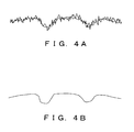
- FIG. 4A illustrates an image signal of an arbitrary line (for example, a line A illustrated in FIG. 3A ) of an object to be shot, on which the noise is superposed.
- FIG. 4B illustrates an image signal after the noise is removed by low pass filter (LPF) processing.
- LPF low pass filter
- FIG. 5 illustrates the output of the image sensor 14 of a conventional imaging apparatus.
- FIG. 5 illustrates the distribution of a level of an output signal of the point image on the image sensor 14 corresponding to an arbitrary point on an object to be shot, and the image forming surface matches the sensor surface to obtain a clear image. Therefore, the distribution of the level of an output signal indicates a waveform of the substantial concentration on one pixel.
- the clearer an image obtained by the imaging apparatus 11 is, the higher frequency noise gets on an image signal by the coarseness of the surface of a medium.
- Performing an operation of low pass filter processing on an image signal output from the image sensor 14 can remove the high frequency noise.
- FIGS. 6A and 6B illustrate the operation matrix of a Gaussian filter and a moving average filter used in the low pass filter processing.
- the 3 ⁇ 3 operation matrix illustrated in FIG. 6A is described below.
- the target pixel Q (a, b) is calculated as a sum of a value obtained by multiplying the upper left pixel data P (a-1, b+1) by "0.063", a value obtained by multiplying the upper pixel data P (a, b+1) by "0.125”, a value obtained by multiplying the upper right pixel data P (a+1, b+1) by "0.063", a value obtained by multiplying the left adjacent pixel data P (a-1, b) by "0.125”, a value obtained by multiplying the pixel data P (a, b) by "0.25", a value obtained by multiplying the right adjacent pixel data P (a+1, b) by "0.125", a value obtained by multiplying the lower left pixel data P (a-1, b-1) by "0.063", a value obtained by multiplying the lower pixel data P (a, b-1) by "0.125”, a value obtained by multiplying the lower right
- An image signal treated by the Gaussian filter processing can be obtained by performing the above-mentioned operation on each pixel.
- the operation matrix illustrated in FIG. 6B is performed, that is, an image signal treated by the moving average filter processing can be obtained by multiplying a target pixel and its peripheral pixels by the value of the operation matrix illustrated in FIG. 6B .
- the patent document 1 describes reducing the distance between a lens and a CCD image pickup element in a fingerprint image read device, and arranging the CCD image pickup element in a position shifted from the focal position of the lens, thereby removing the noise component of a fingerprint image.
- the invention according to the patent document 1 dims high-frequency noise by blurring a fingerprint image to be read by a CCD image pickup element.
- the imaging apparatus for reading information includes an iris for limiting the light-receptive range of the light from an object to be shot, a filter arranged at an aperture of the iris or near the aperture and having the transmittance varying with the position, a lens, and an image sensor.
- the distance between the above mentioned lens and the image sensor is adjusted so that the image forming position can be set in front of or backward the light-receptive surface of the image sensor, thereby spreading the light assigned a desired transmittance characteristic by the filter within a predetermined range.
- the processing time of image processing can be shortened, and a desired low pass filter process can be performed on an image.
- FIG. 7 illustrates a configuration of an imaging apparatus 21 for reading information according to the first embodiment of the present invention.
- the imaging apparatus 21 for reading information according to each embodiment of the present invention described below can be used in a bar code reader for reading a 1- or 2-dimensional bar code, a living body authentication device for reading a vein, etc.
- the imaging apparatus 21 for reading information includes a density filter 22 functioning also as an iris, a lens 23, and an image sensor 24.
- the density filter 22 is arranged between the lens 23 and an object to be shot 25.
- the density filter 22 is an optical filter element functioning as an iris unit 22a for limiting the acceptance angle of light at its periphery, and as a varying density filter unit 22b whose transmittance of light having an optical path limited by the iris unit 22a depends on the position at its central portion.
- An absorbing filter having a variable light absorptance, a reflecting filter having a variable reflectance, etc. can be used as the density filter 22 having a variable transmittance depending on the position on the plane perpendicular to the central axis of the filter and having desired transmittance characteristic (Gaussian distribution etc.).
- the light from the object to be shot 25 enters the density filter 22 while spreading.
- the range of incident light to the lens 23 spreading from each point of the object to be shot 25 (referred to as a luminous flux) is limited by the iris unit 22a of the density filter 22.
- the power of light continuously changes from the center to the periphery of the luminous flux.
- the luminous flux forms an image on an image forming surface (image forming position) 26, it spreads toward the light-receptive surface of the image sensor 24 as an image spreading in a predetermined (certain) range on the light-receptive surface because the distance between the lens 23 and the image sensor 24 is adjusted so that the imaging surface 26 can be set in front of the light-receptive surface of the image sensor 24.
- the image on the light-receptive surface of the image sensor 24 spreads over a plurality of pixels, for example, spreads three pixels in diameter.
- This spread size of the image corresponds to the operational matrix size of the low pass filter, for example, the operation of a 3 ⁇ 3 Gaussian filter illustrated in FIG. 6A can be substituted by the above-mentioned light power distribution of 3 pixels in diameter.
- 3 pixels in diameter can substitute for a 3x 3 circular symmetric operation matrix, such as a Gaussian filter.
- 3x 3 circular symmetric operation matrix such as a Gaussian filter.
- 4.5 pixels in diameter which is the circumscribed circle diameter is preferable.
- a combination of light spread to the circumscribed circle and a variable density filter can substitute for any kind of 3x 3 operation matrix.
- the size of light power distribution is 7 or 9 pixels in diameter, and preferably 10 or 13 pixels in diameter which is the circumscribed circle diameter of the matrix of 7x7 or 9x9 respectively.
- a desired transmittance characteristic is assigned by the density filter 22, and the light spreading on a light-receptive surface in a predetermined range enters the image sensor 24, thereby optically performing a low pass filter process on an image of the object to be shot 25. Therefore, since it is not necessary to perform an operation for the low pass filter process on the output signal of the image sensor 24, the processing time of the image processing can be shortened. In addition, any low pass filter process can be performed by changing the transmittance characteristic of the density filter 22. Furthermore, since the processing time for an image can be shortened, a less expensive CPU of a relatively low processing speed can be used for a bar code reader and a living body authentication device requiring a real-time process. Thus, the cost of the apparatus can be reduced.
- FIG. 8 illustrates the configuration of an imaging apparatus 41 for reading information according to the second embodiment.
- the second embodiment is an example of the case where the image forming surface 26 is set backward the image sensor 24 in the image-side telecentric optical system in which the light from the lens to the image sensor 24 is parallel to the optical axis.
- the optical system of the imaging apparatus 41 for reading information according to the second embodiment includes a lens module 46 configured by lenses 42, 43, 44, and 45 and the density filter 22.
- the imaging apparatus 41 for reading information according to the second embodiment is similar to that according to the first embodiment except that the light incident on the image sensor 24 is parallel to the optical axis, and that the image forming surface 26 is behind the image sensor 24. Because of the image-side telecentric optical system, the image size does not vary when the distance between the lens and the image sensor changes for adjusting the spread size of the incident light on the image sensor surface. This means that the size of LPF can be adjusted independently from the image size and this is an advantage of the second embodiment.
- the reflected light at each point of the object to be shot 25 spreads on the light-receptive surface of the image sensor 24 in a predetermined range, and the power of incident light of each pixel of the image sensor 24 is limited by the transmittance characteristic of the density filter 22.
- a low pass filter process can be optically performed on the light incident from the object to be shot 25.
- the processing time of image processing can be shortened.
- any low pass filter process can be optically realized by changing the transmittance characteristic of the density filter 22.
- FIG. 9 illustrates a configuration of an imaging apparatus 51 for reading information according to the third embodiment of the present invention.
- the third embodiment is basically identical with the second embodiment except that the image forming surface 26 is set in front of the image sensor 24.
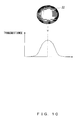
- FIG. 10 illustrates the transmittance characteristic of the density filter 22.
- the density filter 22 is a disk as illustrated in FIG. 10 , indicates the highest transmittance at the center, and decreasing transmittance toward the periphery (for example, a Gaussian distribution).
- the periphery of the density filter 22 has the transmittance of 0, and functions as an iris.
- FIGS. 11 and 12 are other examples of a density filter.
- FIG. 11 is an example of the structure in which a separate density filter 31 is inserted into or attached to an iris 32 having an aperture 32a at the central portion of a non-translucent member of metal etc.
- the density filter 31 is generated by, for example, coating a glass substrate with metal film (for example, chrome film etc.). When metal film is coated, the density filter 31 having any transmittance characteristic such as a Gaussian distribution etc. can be generated by making thinner film at the center and thicker metal film toward the periphery thereby decreasing the transmittance of the light .
- metal film for example, chrome film etc.
- the density filter 31 can be inserted into the aperture 32a of the iris 32, or arranged below the iris 32 near the aperture 32a.
- FIG. 12 is an example of a density filter 33 also functioning as an iris.
- the function of an iris can be realized by setting the transmittance at the periphery of the density filter 33 to 0.
- the periphery can function as an iris unit by thickening the metal film of the periphery and setting the optical transmittance to 0.
- FIG. 13 illustrates the power of incident light of a target pixel a and its peripheral pixels.
- the distance between the lens 23 and the image sensor 24 is adjusted to form an image before the light-receptive surface of the image sensor 24. Therefore, the luminous flux at the point A of the object to be shot 25 forms an image on the image forming surface 26, and then spreads in a predetermined range on the light-receptive surface of the image sensor 24.
- the light passing through the center of the luminous flux from the point A of the object to be shot 25 enters the point A' (refer to FIG. 7 ) of the image sensor 24.
- the light reflected at the point A of the object to be shot 25, passes the position at the right (viewed from the front illustrated in FIG. 7 ) of the density filter 22, and enters the point A' 1 at the left (viewed from the front illustrated in FIG. 7 ) of the point A' of the image sensor 24.
- the light that has passed the position at the left of the density filter 22 enters the point A' 2 at the right to the point A' of the image sensor 24.
- the density filter 22 has the transmittance characteristic of the Gaussian distribution as illustrated in FIG. 10 . Therefore, the light power distribution of the light reflected at the point A of the object to be shot 25, passing through the density filter 22, and entering the image sensor 24 is illustrated in FIG. 13 , and the power of incident light of the target pixel a and its peripheral pixels a+1, a-1, a+2, and a-2 indicates the Gaussian distribution. It is the low pass filter process having the characteristic of the Gaussian distribution optically performed on the reflected light at the point A of the object to be shot 25.
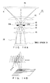
- the operations according to the first, second, and third embodiments are described below with reference to FIGS. 14A, 14B , and 15 . Described below is an example of the case where the density filter 22 is arranged between the lenses in the optical system having a plurality of lenses, and an image is formed in front of the image sensor 24.
- the light reflected at the point A of the object to be shot 25 enters the lenses 42 and 43 while spreading, and the optical path is limited by the iris unit 22a of the density filter 22. Since the density filter 22 has the transmittance characteristic as illustrated in FIG. 10 , the light that has been reflected at the point A, and passed through the density filter 22 has the highest optical transmittance at the center of the luminous flux, and the decreasing transmittance toward the periphery.
- the light that has passed through the density filter 22 is converted into light parallel to the optical axis by the lenses 44 and 45, forms an image on the image forming surface 26, and spreads in a predetermined range (for example, a range having three or more pixels in diameter) on the light-receptive surface of the image sensor 24.
- a predetermined range for example, a range having three or more pixels in diameter
- FIG. 14B illustrates the distribution of the power of incident light of each pixel of the image sensor 24.
- the reflected light at the point A of the object to be shot 25 enters the corresponding pixel of the image sensor 24 and its peripheral pixels.
- the reflected light at the point A indicates the Gaussian distribution, that is, the power of incident light of the central pixel (target pixel a in FIG. 13 ) which the light at the center of the luminous flux enters is the largest, and the power of incident light decreases for a farther pixel from the central pixel.
- the reflected light at the point next to the point A of the object to be shot 25 indicates the Gaussian distribution, in which the power of incident light of the pixel next to the point a (pixel a+1 in FIG. 13 ) on the image sensor 24 is the largest, and it decreases for a farther pixel from the central pixel.
- the power of incident light of each of other pixels of the image sensor 24 indicates the Gaussian distribution as illustrated in FIG. 14B .
- the light from the point A of the object to be shot 25 enters a corresponding pixel a of the image sensor 24 and a plurality of adjacent pixels a+1, a-1, a+2, a-2, ... with the light power distribution depending on the transmittance characteristic of the density filter 22. Simultaneously, a part of the incident light centering on the pixel a+1, a-1, a+2, a-2, or other adjacent pixels also enters the pixel a. Thus, an optical convolution is performed. It means that the conventional process of the low pass filter operation performed by the convolutional operation on the output signal of the image sensor 24 is optically replaced.
- FIG. 15 illustrates the power of incident light at an arbitrary pixel array of the image sensor 24.
- the light (luminous flux) from the point A of the object to be shot 25 enters the density filter 22 while spreading, but the incident light is limited by the iris unit 22a, and the luminous flux passing through the density filter unit 22b indicates continuously decreasing transmittance from the center of the luminous flux toward the periphery according to the transmittance characteristic of the density filter 22.
- the luminous flux temporarily forms an image, but spreads in a predetermined range (for example, a range of a diameter of a length of three pixels from the center of the luminous flux) when it enters the image sensor 24.
- the luminous flux that is reflected at each point of the object to be shot 25, passes through the density filter 22, and enters the image sensor 24 has a predetermined light power distribution centering on the target pixel on which the central light of the luminous flux enters.
- the light reflected at the point A of the object to be shot 25 has the power distribution which indicates the Gaussian distribution illustrated in FIG. 10 centering on the pixel a.
- the light having the adjacent pixels a+1, a-1, a+2, a-2, ... as the center also enters the pixel a, thereby optically performing a convolutional operation.
- the power of the reflected light at each point of the object to be shot 25 is limited by the transmittance characteristic of the density filter 22 and enters the 24, for example, when the density filter 22 has the characteristic of the Gaussian distribution, a low pass filter process having the Gaussian distribution can be performed on the light incident on the image sensor 24.
- a low pass filter process can be optically performed on the light incident from the object to be shot 25.
- the transmittance distribution of the density filter 22 is defined as a Gaussian distribution
- the light power distribution of the point image on the image sensor 24 obtained as a result is also defined as a Gaussian distribution for simple explanation.
- the basic optical system itself commonly has not a flat power distribution but a specific light power distribution, the two distributions do not necessarily match. Therefore, to correctly define the light power distribution on the image sensor 24 as a Gaussian distribution, it is necessary to adjust in advance the transmittance distribution of the density filter 22 to offset the distribution specific to the basic optical system. The process is described below in detail with reference to FIGS. 16A and 16B .
- FIGS. 16A and 16B illustrate the relationships between the transmittance characteristic of the density filter 22 and the power of received light of the image sensor 24 when there is and is not a density filter at the aperture of the iris.
- FIG. 16A illustrates the radius direction of the density filter 22
- FIG. 16B illustrates the relationship between the distance r in the radius direction from the center of the density filter 22 and the transmittance, and the relationship between the distance from the center of the target pixel (point A' in FIG. 7 ) of the image sensor 24 and the power of light.
- the horizontal axis in FIG. 16B indicates the distance from the center of the density filter 22 and the distance from the center of the target pixel while the vertical axis indicates the transmittance and the power of light.
- the graph of the solid line in FIG. 16B indicates the transmittance of the density filter 22, and the graphs of the dotted line indicate the light power distributions on the image sensor 24 with and without a density filter.
- the light power distribution at the point A' (without a density filter) indicated by the dotted line in FIG. 16B is the light power distribution on the image sensor 24 when the density filter 22 is not used while the image is out of focus with the image forming surface 26 of the lens 23 shifted before or backward the light-receptive surface of the image sensor 24.
- the density filter 22 since the density filter 22 is not used, the light power distribution of the pixels in the predetermined range centering on the target pixel (pixel at the point A') is trapezoidal, but it is not completely trapezoidal because a lens or a lens module generally can collect less power of light at the periphery than the central portion of the captured image, and the light power distribution indicates a decreasing power of light with a larger r as indicated by the dotted line (the low pass filter effect can be obtained as is, but is limited by a low pass filter having a specific characteristic).
- the light power distribution at the point A' (with a density filter) indicated by the dotted line in FIG. 16B is the light power distribution of the image sensor 24 when the density filter 22 is used while the image is out of focus with the image forming surface 26 of the lens 23 shifted before or backward the light-receptive surface of the image sensor 24.
- the light power distribution of the pixels in a predetermined range centering on the target pixel (pixel at the point A') is a combination of the transmittance characteristic of the density filter 22 and the light power distribution without a density filter.
- the transmittance distribution of the density filter indicated by the solid line is not defined as a Gaussian distribution, but the light power distribution without a density filter, that is, the light power distribution specific to the basic optical system is to be offset.
- any low pass filter process other than the Gaussian distribution can be optically performed on the light incident on the image sensor 24.
- the processing time of image processing can be shortened in the imaging apparatus for reading information, and a desired low pass filter process can be optically performed on an image.
- a less expensive CPU of a relatively low processing speed can be used for an imaging apparatus for reading information that has to perform a real-time process by shortening the processing time of image processing, the cost of the imaging apparatus for reading information can be reduced.
- embodiments of the present invention can also be applied to a case where a low pass filter characteristic other than the Gaussian distribution is used.
- Embodiments of the present invention can also be applied to an optical system configured by a plurality of lenses other than an image-side telecentric optical system.
Landscapes
- Physics & Mathematics (AREA)
- General Physics & Mathematics (AREA)
- Engineering & Computer Science (AREA)
- Optics & Photonics (AREA)
- Multimedia (AREA)
- Vascular Medicine (AREA)
- Health & Medical Sciences (AREA)
- Theoretical Computer Science (AREA)
- General Health & Medical Sciences (AREA)
- Image Input (AREA)
- Studio Devices (AREA)
- Optical Elements Other Than Lenses (AREA)
- Lenses (AREA)
- Cash Registers Or Receiving Machines (AREA)
- Facsimile Scanning Arrangements (AREA)
Applications Claiming Priority (1)
| Application Number | Priority Date | Filing Date | Title |
|---|---|---|---|
| JP2008254848A JP5676843B2 (ja) | 2008-09-30 | 2008-09-30 | 情報読取用撮像装置 |
Publications (2)
| Publication Number | Publication Date |
|---|---|
| EP2169440A2 true EP2169440A2 (de) | 2010-03-31 |
| EP2169440A3 EP2169440A3 (de) | 2010-06-16 |
Family
ID=41566250
Family Applications (1)
| Application Number | Title | Priority Date | Filing Date |
|---|---|---|---|
| EP09170608A Withdrawn EP2169440A3 (de) | 2008-09-30 | 2009-09-17 | Bildgebungsvorrichtung zum Lesen von Informationen |
Country Status (5)
| Country | Link |
|---|---|
| US (1) | US8345149B2 (de) |
| EP (1) | EP2169440A3 (de) |
| JP (1) | JP5676843B2 (de) |
| KR (1) | KR101081683B1 (de) |
| CN (1) | CN101715036B (de) |
Cited By (2)
| Publication number | Priority date | Publication date | Assignee | Title |
|---|---|---|---|---|
| EP3623921A4 (de) * | 2018-08-02 | 2020-06-10 | Shenzhen Goodix Technology Co., Ltd. | Vorrichtung zur biometrischen identifizierung unter dem bildschirm und elektronische vorrichtung |
| JPWO2021261295A1 (de) * | 2020-06-25 | 2021-12-30 |
Families Citing this family (5)
| Publication number | Priority date | Publication date | Assignee | Title |
|---|---|---|---|---|
| KR101704591B1 (ko) * | 2012-02-21 | 2017-02-08 | 에이에스엠엘 네델란즈 비.브이. | 검사 장치 및 방법 |
| CN102902004B (zh) * | 2012-11-01 | 2015-05-20 | 沈阳仪表科学研究院 | 环形双向渐深变密度片 |
| US9588400B2 (en) * | 2013-03-27 | 2017-03-07 | Ricoh Imaging Company, Ltd. | Photographing apparatus and photographing control system |
| JP6442065B2 (ja) * | 2015-09-16 | 2018-12-19 | 富士フイルム株式会社 | フォーカス装置,撮像システムおよびフォーカス駆動信号出力方法 |
| CN109740397A (zh) * | 2018-12-26 | 2019-05-10 | 深圳盈达信息科技有限公司 | 一种扫描引擎及扫描装置 |
Citations (1)
| Publication number | Priority date | Publication date | Assignee | Title |
|---|---|---|---|---|
| JP2003050991A (ja) | 2001-08-03 | 2003-02-21 | Sony Corp | 指紋画像読取装置及び指紋照合装置 |
Family Cites Families (13)
| Publication number | Priority date | Publication date | Assignee | Title |
|---|---|---|---|---|
| US5111343A (en) * | 1990-05-29 | 1992-05-05 | Eastman Kodak Company | Gradient filter |
| US5541779A (en) * | 1993-11-17 | 1996-07-30 | Daewoo Electronics Co., Ltd. | Optical imaging system |
| JP3070484B2 (ja) * | 1995-07-26 | 2000-07-31 | 株式会社デンソー | 光学情報読取装置および光学情報読取方法 |
| JPH0983858A (ja) * | 1995-09-12 | 1997-03-28 | Canon Inc | 撮像装置および撮像方法 |
| US6587148B1 (en) * | 1995-09-01 | 2003-07-01 | Canon Kabushiki Kaisha | Reduced aliasing distortion optical filter, and an image sensing device using same |
| US7099555B2 (en) * | 2003-08-20 | 2006-08-29 | Canon Kabushiki Kaisha | Light amount adjusting apparatus, optical equipment, optical filter and image-taking apparatus |
| JP2005266096A (ja) * | 2004-03-17 | 2005-09-29 | Canon Inc | 光学フィルタ及び撮影装置 |
| DE102004013850B4 (de) * | 2004-03-20 | 2006-12-21 | Robert Bosch Gmbh | Filterchip mit integrierter Blende |
| GB0406730D0 (en) * | 2004-03-25 | 2004-04-28 | 1 Ltd | Focussing method |
| DE102004028616A1 (de) * | 2004-06-12 | 2006-02-02 | Robert Bosch Gmbh | Kameraobjektiv |
| JP2006030602A (ja) * | 2004-07-16 | 2006-02-02 | Konica Minolta Opto Inc | 光学ユニット |
| JP2007140176A (ja) * | 2005-11-18 | 2007-06-07 | Nikon Corp | 電子カメラ |
| JP2008028963A (ja) * | 2006-07-25 | 2008-02-07 | Ricoh Co Ltd | 画像入力装置 |
-
2008
- 2008-09-30 JP JP2008254848A patent/JP5676843B2/ja active Active
-
2009
- 2009-09-16 KR KR1020090087361A patent/KR101081683B1/ko not_active Expired - Fee Related
- 2009-09-16 CN CN2009101775923A patent/CN101715036B/zh not_active Expired - Fee Related
- 2009-09-17 US US12/561,870 patent/US8345149B2/en active Active
- 2009-09-17 EP EP09170608A patent/EP2169440A3/de not_active Withdrawn
Patent Citations (1)
| Publication number | Priority date | Publication date | Assignee | Title |
|---|---|---|---|---|
| JP2003050991A (ja) | 2001-08-03 | 2003-02-21 | Sony Corp | 指紋画像読取装置及び指紋照合装置 |
Cited By (3)
| Publication number | Priority date | Publication date | Assignee | Title |
|---|---|---|---|---|
| EP3623921A4 (de) * | 2018-08-02 | 2020-06-10 | Shenzhen Goodix Technology Co., Ltd. | Vorrichtung zur biometrischen identifizierung unter dem bildschirm und elektronische vorrichtung |
| US10963667B2 (en) | 2018-08-02 | 2021-03-30 | Shenzhen GOODIX Technology Co., Ltd. | Under-screen biometric identification apparatus and electronic device |
| JPWO2021261295A1 (de) * | 2020-06-25 | 2021-12-30 |
Also Published As
| Publication number | Publication date |
|---|---|
| KR20100036940A (ko) | 2010-04-08 |
| CN101715036B (zh) | 2013-08-07 |
| KR101081683B1 (ko) | 2011-11-09 |
| EP2169440A3 (de) | 2010-06-16 |
| JP2010087849A (ja) | 2010-04-15 |
| JP5676843B2 (ja) | 2015-02-25 |
| US20100079657A1 (en) | 2010-04-01 |
| CN101715036A (zh) | 2010-05-26 |
| US8345149B2 (en) | 2013-01-01 |
Similar Documents
| Publication | Publication Date | Title |
|---|---|---|
| US8345149B2 (en) | Imaging apparatus for reading information | |
| USRE43089E1 (en) | Imaging system with a lens having increased light collection efficiency and a deblurring equalizer | |
| US20150269403A1 (en) | Barcode reader having multiple sets of imaging optics | |
| CN108702440B (zh) | 摄像装置 | |
| JP3877058B2 (ja) | 小型装置およびその製造方法 | |
| US8306287B2 (en) | Biometrics authentication system | |
| US10769400B2 (en) | Barcode reader | |
| EP3340600B1 (de) | Linse, kamera, packungsinspektionssystem und bildverarbeitungsverfahren | |
| US8387880B2 (en) | Imaging apparatus for reading information | |
| US20100079658A1 (en) | Lens unit, image pickup apparatus, electronic device and an image aberration control method | |
| JP2007071979A (ja) | 結像光学系及びそれを用いた撮像装置、認証装置 | |
| JP2022545748A (ja) | Tofカメラ | |
| CN102880867B (zh) | 光学指纹采集装置 | |
| JP5080414B2 (ja) | 情報読取用撮像装置 | |
| CN110166676B (zh) | 一种成像设备、成像控制方法、电子装置和介质 | |
| CN116953883A (zh) | 一种激光对焦方法、装置、电子设备和存储介质 | |
| EP3370410B1 (de) | Bildgebungsvorrichtung | |
| JP4352763B2 (ja) | デジタル通信光学系及びこれに用いる集光素子 | |
| JP2017207450A (ja) | 撮像光学系及び撮像装置 | |
| RU75296U1 (ru) | Анаморфотная система считывания папиллярных рисунков крайних фаланг пальцев | |
| RU63570U1 (ru) | Анаморфотная система считывания папиллярных рисунков пальцев и ладони | |
| JPS61154360A (ja) | 光量補正板 | |
| Alex et al. | Optics beyond Optical Barriers-General Approach | |
| JPH11203460A (ja) | パターン読み取り装置 |
Legal Events
| Date | Code | Title | Description |
|---|---|---|---|
| PUAI | Public reference made under article 153(3) epc to a published international application that has entered the european phase |
Free format text: ORIGINAL CODE: 0009012 |
|
| AK | Designated contracting states |
Kind code of ref document: A2 Designated state(s): AT BE BG CH CY CZ DE DK EE ES FI FR GB GR HR HU IE IS IT LI LT LU LV MC MK MT NL NO PL PT RO SE SI SK SM TR |
|
| AX | Request for extension of the european patent |
Extension state: AL BA RS |
|
| PUAL | Search report despatched |
Free format text: ORIGINAL CODE: 0009013 |
|
| AK | Designated contracting states |
Kind code of ref document: A3 Designated state(s): AT BE BG CH CY CZ DE DK EE ES FI FR GB GR HR HU IE IS IT LI LT LU LV MC MK MT NL NO PL PT RO SE SI SK SM TR |
|
| AX | Request for extension of the european patent |
Extension state: AL BA RS |
|
| RIC1 | Information provided on ipc code assigned before grant |
Ipc: G02B 5/20 20060101ALI20100510BHEP Ipc: G02B 13/20 20060101AFI20100201BHEP Ipc: G06K 9/20 20060101ALI20100510BHEP |
|
| 17P | Request for examination filed |
Effective date: 20101213 |
|
| 17Q | First examination report despatched |
Effective date: 20140407 |
|
| STAA | Information on the status of an ep patent application or granted ep patent |
Free format text: STATUS: THE APPLICATION IS DEEMED TO BE WITHDRAWN |
|
| 18D | Application deemed to be withdrawn |
Effective date: 20170401 |