EP2164174A2 - Method and circuit to increase breakdown voltage of MOS transistors at low temperatures - Google Patents
Method and circuit to increase breakdown voltage of MOS transistors at low temperatures Download PDFInfo
- Publication number
- EP2164174A2 EP2164174A2 EP09168721A EP09168721A EP2164174A2 EP 2164174 A2 EP2164174 A2 EP 2164174A2 EP 09168721 A EP09168721 A EP 09168721A EP 09168721 A EP09168721 A EP 09168721A EP 2164174 A2 EP2164174 A2 EP 2164174A2
- Authority
- EP
- European Patent Office
- Prior art keywords
- metal oxide
- circuit arrangement
- voltage
- oxide transistor
- transistor
- Prior art date
- Legal status (The legal status is an assumption and is not a legal conclusion. Google has not performed a legal analysis and makes no representation as to the accuracy of the status listed.)
- Withdrawn
Links
Images
Classifications
-
- H—ELECTRICITY
- H01—ELECTRIC ELEMENTS
- H01L—SEMICONDUCTOR DEVICES NOT COVERED BY CLASS H10
- H01L23/00—Details of semiconductor or other solid state devices
- H01L23/34—Arrangements for cooling, heating, ventilating or temperature compensation ; Temperature sensing arrangements
- H01L23/345—Arrangements for heating
-
- H—ELECTRICITY
- H03—ELECTRONIC CIRCUITRY
- H03K—PULSE TECHNIQUE
- H03K19/00—Logic circuits, i.e. having at least two inputs acting on one output; Inverting circuits
- H03K19/003—Modifications for increasing the reliability for protection
- H03K19/00315—Modifications for increasing the reliability for protection in field-effect transistor circuits
-
- H—ELECTRICITY
- H03—ELECTRONIC CIRCUITRY
- H03K—PULSE TECHNIQUE
- H03K19/00—Logic circuits, i.e. having at least two inputs acting on one output; Inverting circuits
- H03K19/003—Modifications for increasing the reliability for protection
- H03K19/00369—Modifications for compensating variations of temperature, supply voltage or other physical parameters
- H03K19/00384—Modifications for compensating variations of temperature, supply voltage or other physical parameters in field effect transistor circuits
-
- H—ELECTRICITY
- H01—ELECTRIC ELEMENTS
- H01L—SEMICONDUCTOR DEVICES NOT COVERED BY CLASS H10
- H01L2924/00—Indexing scheme for arrangements or methods for connecting or disconnecting semiconductor or solid-state bodies as covered by H01L24/00
- H01L2924/0001—Technical content checked by a classifier
- H01L2924/0002—Not covered by any one of groups H01L24/00, H01L24/00 and H01L2224/00
-
- H—ELECTRICITY
- H01—ELECTRIC ELEMENTS
- H01L—SEMICONDUCTOR DEVICES NOT COVERED BY CLASS H10
- H01L2924/00—Indexing scheme for arrangements or methods for connecting or disconnecting semiconductor or solid-state bodies as covered by H01L24/00
- H01L2924/10—Details of semiconductor or other solid state devices to be connected
- H01L2924/11—Device type
- H01L2924/13—Discrete devices, e.g. 3 terminal devices
- H01L2924/1304—Transistor
- H01L2924/1306—Field-effect transistor [FET]
- H01L2924/13091—Metal-Oxide-Semiconductor Field-Effect Transistor [MOSFET]
Definitions
- the invention relates to a method for increasing the temperature-independent dielectric strength of electronic circuit arrangements with metal oxide according to the preamble of the main claim, and of a circuit arrangement with at least one metal oxide and an elevated temperature-independent withstand voltage according to the preamble of the independent claim.
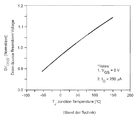
- the single FIGURE shows a graph of the normalized breakdown voltage of a metal oxide transistor according to the prior art, also abbreviated to MOSFET, plotted against the chip temperature. It can clearly be seen that the breakdown voltage of the metal oxide transistor also drops considerably as the temperature of the metal oxide transistor decreases. This raises the problem that the withstand voltage of an entire circuit including such a metal oxide transistor also decreases at low temperatures. To circumvent this problem, metal oxide transistors with higher blocking voltage have hitherto been used. However, these are considerably more expensive and have disadvantages such as higher channel resistance (RDS On ). The problem is particularly serious if, due to the boundary conditions, metal oxide transistors must be selected which exceed a voltage level due to technology.
- RDS On higher channel resistance
- the object is achieved with respect to the method according to the invention with a method for increasing the dielectric strength of an electronic circuit arrangement at low temperatures, wherein the circuit arrangement has at least one metal oxide transistor, and before applying a voltage which is in the vicinity of the breakdown voltage of the metal oxide, this is heated by suitable means to a predetermined temperature.
- the heating of the metal oxide transistor is achieved by a high current through the metal oxide transistor.
- the heating of the metal oxide transistor is accomplished by increasing the switching losses of the metal oxide transistor.
- the heating of the metal oxide transistor is accomplished by a short-term linear operation of the metal oxide transistor.
- the heating can be either time-controlled or temperature-controlled.
- the timed variant heats the metal oxide transistor for a predetermined time. It offers the advantage of a cost-effective implementation.
- the temperature controlled variant measures the temperature of the circuitry or metal oxide transistor and heats it to a predetermined temperature (e.g., 25 ° C). It offers the advantage of good temperature control of the metal oxide transistor.
- the heating is preferably accomplished only at low temperatures of the circuit or the metal oxide. This prevents overheating of the metal oxide at higher temperatures of the circuit or the metal oxide transistor.
- circuit arrangement with an increased dielectric strength at low temperatures, wherein the circuit arrangement comprises at least one metal oxide, and it has means for heating the metal oxide before it reaches a voltage in the vicinity of the reverse voltage of the metal oxide lies, touches him.
- the heating of the metal oxide transistor is achieved by a high current through the metal oxide transistor.
- the heating of the metal oxide transistor is accomplished by increasing the switching losses of the metal oxide transistor.
- the heating of the metal oxide transistor is accomplished by a short-term linear operation of the metal oxide transistor.
- the circuit arrangement preferably heats the latter only at low temperatures of the circuit arrangement or of the metal oxide transistor. This prevents overheating of the metal oxide at higher temperatures of the circuit or the metal oxide transistor.
- the heating can be either time-controlled or temperature-controlled.
- the timed variant offers the advantage of a cost-effective implementation.
- the temperature controlled version offers the advantage of a precise temperature control of the metal oxide transistor.
- the circuit arrangement preferably measures the temperature of the metal oxide transistor. Particularly preferably, the temperature of the metal oxide transistor is measured via its channel resistance. This offers the advantage of a simple and inexpensive implementation of the temperature measurement.
- the circuit arrangement is preferably designed to operate at least one gas discharge lamp, wherein it generates an intermediate circuit voltage for application to the metal oxide transistor, and heats the metal oxide transistor shortly before the start of the gas discharge lamp or at the start of the gas discharge lamp.
- just before the start means that the circuit uses the time before the lamp start in which it builds the ignition voltage for the heating of the metal oxide transistor.
- the DC link voltage is advantageously lowered during the heating phase, and the heating phase between 1s and 120s long. By lowering the DC link voltage, the metal oxide transistor is protected, and the length of the heating phase guarantees effective heating of the transistor.
- the lowering of the intermediate circuit voltage is preferably accomplished by a DC-DC converter having an adjustable output voltage, and whose output voltage is the intermediate circuit voltage. Since a DC-DC converter is used in many cases for other reasons, it is advantageous to make this existing DC-DC converter with little effort in its output voltage adjustable to adjust the DC link voltage can.
- a metal oxide transistor having no increased reverse voltage can be used.
- the latter prior to application of a voltage to the metal oxide transistor, which lies in the region of the blocking voltage of the metal oxide transistor, the latter is heated to a temperature at which it can reliably block the voltage to be applied.
- the temperature dependence of the blocking voltage of metal oxide transistors is utilized.
- the metal oxide transistor is used as a switching transistor in the inverter of an electronic control gear for gas discharge lamps.
- the inverter is often preceded by a DC-DC converter, for example, a power factor correction can perform.
- the DC-DC converter can be designed for example as a boost, Sepic or flyback converter.
- the DC-DC converter generates a regulated output voltage that is input to the inverter. This voltage is often referred to as a DC link voltage.
- the inverter can be designed as a Class-E converter, as a half-bridge inverter or as a full-bridge inverter. Accordingly, the inverter has between one and four metal oxide transistors. In such an operating device, these metal oxide transistors are often operated near the blocking voltage in continuous lamp operation.
- the lamp voltage of the gas discharge lamp to be operated is thus in the range of the blocking voltage of the metal oxide transistor.
- the electronic control gear for outdoor applications at low ambient temperatures of eg -40 ° C or even applications can be specified in cold stores, which then entail a correspondingly low temperature of the circuit or the Metalloxidtransistors, it is necessary, the or the Metalloxidtransistoren accordingly preheat so that they can lock the rapidly increasing lamp voltage of the gas discharge lamp after starting.
- the period of time in which the metal oxide transistor is preheated, and therefore in which the voltage applied to the transistor, for example the intermediate circuit voltage, is lowered, is between 1 s and 120 s.
- the metal oxide transistor can be heated by various methods. Many operating devices ignite the high-pressure discharge lamps by means of a resonance ignition, similar to the case with low-pressure discharge lamps. During this resonant phase, a high current flows through the metal oxide transistor, which can heat it up quickly and reliably. In order to optimize the heating, the metal oxide transistor may be operated in the linear region for a short period of time during the resonance ignition to accelerate the heat input to the transistor. This short period of time during which the metal oxide transistor has a higher on-resistance (R DSOn ) during which resonance is attenuated is imperceptible to the user.
- R DSOn on-resistance
- Another variant is to heat the metal oxide during the heating of the high pressure discharge lamp. Shortly after ignition, a high-pressure discharge lamp still has a rather low lamp voltage, which rises steadily during the start-up of the lamp. During this time, the metal oxide transistor can also be heated without running the risk of being destroyed by overvoltage. The heating takes place again by increased switching losses during the heating phase.
- the increased switching losses can be caused, for example, by a capacitive operation of the metal oxide transistor, or by an increase in the switching frequency, which increases the losses per unit time.
- the increase of the switching frequency has the advantage that thereby the voltage switched by the metal oxide transistor voltage can be lowered, without a fading of the arc must be feared.
- both options are combined, and the transistor is heated during the ignition of the high-pressure discharge lamp and also during the start-up of the high-pressure discharge lamp.
- the DC link voltage can be lowered by the DC-DC converter, since, as already mentioned above, the lamp voltage is correspondingly low. This ensures that the metal oxide transistor can safely block the voltage applied to it.
- One way to control the heating phases is to measure the metal oxide transistor temperature. This can be done by a temperature sensor attached to the metal oxide transistor or by means of the sheet resistance of the metal oxide transistor. The track resistance can be measured by means of a temperature-compensated measuring arrangement, and thus the chip temperature of the metal oxide transistor can be determined. The heating phases are then controlled until the transistor has reached a predetermined minimum temperature (e.g., + 25 ° C).
- a predetermined minimum temperature e.g., + 25 ° C.
- the metal oxide transistor may drop below a predetermined temperature. Then additional heating phases are to be provided even in normal operation in order to ensure safe operation of the metal oxide transistor.
- the heating phases can be implemented as described above in the operation of the high pressure discharge lamp. In this connection, a linear operation of the metal oxide transistor and / or a temporary turn-off of the zero-voltage switching (ZVS) of the metal oxide transistor or the current-free switching (ZCS) of the metal oxide transistor is preferable to the other described methods.
Landscapes
- Physics & Mathematics (AREA)
- Engineering & Computer Science (AREA)
- Computer Hardware Design (AREA)
- Computing Systems (AREA)
- General Engineering & Computer Science (AREA)
- Mathematical Physics (AREA)
- Condensed Matter Physics & Semiconductors (AREA)
- General Physics & Mathematics (AREA)
- Microelectronics & Electronic Packaging (AREA)
- Power Engineering (AREA)
- General Induction Heating (AREA)
- Semiconductor Integrated Circuits (AREA)
- Circuit Arrangements For Discharge Lamps (AREA)
- Electronic Switches (AREA)
Abstract
Description
Die Erfindung betrifft ein Verfahren zur Erhöhung der temperaturunabhängigen Spannungsfestigkeit elektronischer Schaltungsanordnungen mit Metalloxidtransistoren nach der Gattung des Hauptanspruchs, sowie von einer Schaltungsanordnung mit mindestens einem Metalloxidtransistor und einer erhöhten temperaturunabhängigen Spannungsfestigkeit nach der Gattung des Nebenanspruchs.The invention relates to a method for increasing the temperature-independent dielectric strength of electronic circuit arrangements with metal oxide according to the preamble of the main claim, and of a circuit arrangement with at least one metal oxide and an elevated temperature-independent withstand voltage according to the preamble of the independent claim.
Die einzige Fig. zeigt ein Diagramm der normierten Durchbruchsspannung eines Metalloxidtransistors nach dem Stand der Technik, in der Abkürzung auch MOSFET genannt, über der Chiptemperatur aufgetragen. Es ist deutlich zu sehen, dass die Durchbruchsspannung des Metalloxidtransistors bei sinkender Temperatur des Metalloxidtransistors ebenfalls erheblich sinkt. Dies wirft das Problem auf, dass die Spannungsfestigkeit einer gesamten Schaltungsanordnung, die solch einen Metalloxidtransistor aufweist, bei niedrigen Temperaturen ebenfalls sinkt. Um dieses Problem zu umgehen sind bisher Metalloxidtransistoren mit höherer Sperrspannung verwendet worden. Diese sind jedoch erheblich teurer, und weisen Nachteile wie einen höheren Kanalwiderstand (RDSOn) auf. Besonders gravierend zeigt sich das Problem, wenn aufgrund der Randbedingungen Metalloxidtransistoren ausgewählt werden müssen, die einen technologiebedingten Spannungslevel überschreiten. Wird solch ein Level überschritten, kommen andere Halbleiterchips im Transistor zum Einsatz, die aufgrund einer anderen Fertigungstechnologie deutlich kostenaufwändiger sind. In solch einem Fall ist für einen Metalloxidtransistor mit höherer Sperrspannung mit erheblichen Mehrkosten zu rechnen. Alternativ kann für die Schaltungsanordnung ein engerer Temperaturbereich spezifiziert werden. Dies ist aber aufgrund der Anwendung oftmals nicht möglich.The single FIGURE shows a graph of the normalized breakdown voltage of a metal oxide transistor according to the prior art, also abbreviated to MOSFET, plotted against the chip temperature. It can clearly be seen that the breakdown voltage of the metal oxide transistor also drops considerably as the temperature of the metal oxide transistor decreases. This raises the problem that the withstand voltage of an entire circuit including such a metal oxide transistor also decreases at low temperatures. To circumvent this problem, metal oxide transistors with higher blocking voltage have hitherto been used. However, these are considerably more expensive and have disadvantages such as higher channel resistance (RDS On ). The problem is particularly serious if, due to the boundary conditions, metal oxide transistors must be selected which exceed a voltage level due to technology. If such a level is exceeded, come other semiconductor chips in the transistor are used, which are significantly more expensive due to a different manufacturing technology. In such a case, a metal oxide transistor with higher blocking voltage can be expected to incur significant additional costs. Alternatively, a narrower temperature range can be specified for the circuit arrangement. However, this is often not possible due to the application.
Es ist Aufgabe der Erfindung, ein Verfahren zur Erhöhung der Spannungsfestigkeit einer elektronischen Schaltungsanordnung bei niedrigen Temperaturen anzugeben, wobei die Schaltungsanordnung mindestens einen Metalloxidtransistor aufweist, und auf die Auswahl eines Metalloxidtransistors mit höherer Sperrspannung verzichtet werden kann.It is an object of the invention to provide a method for increasing the dielectric strength of an electronic circuit arrangement at low temperatures, wherein the circuit arrangement has at least one metal oxide, and can be dispensed with the selection of a metal oxide transistor with higher blocking voltage.
Es ist ebenfalls Aufgabe der Erfindung, eine Schaltungsanordnung mit einer erhöhten Spannungsfestigkeit bei niedrigen Temperaturen anzugeben, wobei die Schaltungsanordnung mindestens einen Metalloxidtransistor aufweist, ohne dass der Metalloxidtransistor eine höhere Sperrspannung aufweist.It is also an object of the invention to provide a circuit arrangement with an increased dielectric strength at low temperatures, the circuit arrangement having at least one metal oxide transistor, without the metal oxide transistor having a higher blocking voltage.
Die Lösung der Aufgabe bezüglich des Verfahrens erfolgt erfindungsgemäß mit einem Verfahren zur Erhöhung der Spannungsfestigkeit einer elektronischen Schaltungsanordnung bei niedrigen Temperaturen, wobei die Schaltungsanordnung mindestens einen Metalloxidtransistor aufweist, und vor dem Anlegen einer Spannung, die in der Nähe der Durchbruchsspannung des Metalloxidtransistors liegt, dieser durch geeignete Maßnahmen auf eine vorbestimmte Temperatur aufgeheizt wird.The object is achieved with respect to the method according to the invention with a method for increasing the dielectric strength of an electronic circuit arrangement at low temperatures, wherein the circuit arrangement has at least one metal oxide transistor, and before applying a voltage which is in the vicinity of the breakdown voltage of the metal oxide, this is heated by suitable means to a predetermined temperature.
In einer ersten Variante wird das Aufheizen des Metalloxidtransistors dabei durch einen hohen Strom durch den Metalloxidtransistor erreicht. In einer weiteren Variante wird das Aufheizen des Metalloxidtransistors durch eine Erhöhung der Schaltverluste des Metalloxidtransistors bewerkstelligt. In einer dritten Variante wird das Aufheizen des Metalloxidtransistors durch einen kurzzeitigen linearen Betrieb des Metalloxidtransistors bewerkstelligt. Diese Varianten stellen ein schnelles und zuverlässiges Aufheizen des Metalloxidtransistors sicher.In a first variant, the heating of the metal oxide transistor is achieved by a high current through the metal oxide transistor. In a further variant, the heating of the metal oxide transistor is accomplished by increasing the switching losses of the metal oxide transistor. In a third variant, the heating of the metal oxide transistor is accomplished by a short-term linear operation of the metal oxide transistor. These variants ensure fast and reliable heating of the metal oxide transistor.
Das Aufheizen kann dabei entweder zeitgesteuert oder temperaturgesteuert erfolgen. Die Zeitgesteuerte Variante heizt den Metalloxidtransistor für eine vorbestimmte Zeit auf. Sie bietet den Vorteil einer kostengünstigen Implementierung. Die temperaturgesteuerte Variante misst die Temperatur der Schaltungsanordnung oder des Metalloxidtransistors und heizt ihn auf eine vorbestimmte Temperatur (z.B. 25°C) auf. Sie bietet den Vorteil einer guten Temperaturregelung des Metalloxidtransistors.The heating can be either time-controlled or temperature-controlled. The timed variant heats the metal oxide transistor for a predetermined time. It offers the advantage of a cost-effective implementation. The temperature controlled variant measures the temperature of the circuitry or metal oxide transistor and heats it to a predetermined temperature (e.g., 25 ° C). It offers the advantage of good temperature control of the metal oxide transistor.
Das Aufheizen wird dabei vorzugsweise nur bei niedrigen Temperaturen der Schaltungsanordnung beziehungsweise des Metalloxidtransistors bewerkstelligt. Dies verhindert eine Überhitzung des Metalloxidtransistors bei höheren Temperaturen der Schaltungsanordnung beziehungsweise des Metalloxidtransistors.The heating is preferably accomplished only at low temperatures of the circuit or the metal oxide. This prevents overheating of the metal oxide at higher temperatures of the circuit or the metal oxide transistor.
Die Lösung der Aufgabe bezüglich der Schaltungsanordnung erfolgt erfindungsgemäß mit einer Schaltungsanordnung mit einer erhöhten Spannungsfestigkeit bei niedrigen Temperaturen, wobei die Schaltungsanordnung mindestens einen Metalloxidtransistor aufweist, und sie Mittel zum Aufheizen des Metalloxidtransistors aufweist, bevor sie eine Spannung, die in der Nähe der Sperrspannung des Metalloxidtransistors liegt, an ihn anlegt.The solution of the object with respect to the circuit arrangement according to the invention with a circuit arrangement with an increased dielectric strength at low temperatures, wherein the circuit arrangement comprises at least one metal oxide, and it has means for heating the metal oxide before it reaches a voltage in the vicinity of the reverse voltage of the metal oxide lies, touches him.
In einer ersten Variante wird das Aufheizen des Metalloxidtransistors dabei durch einen hohen Strom durch den Metalloxidtransistor erreicht. In einer weiteren Variante wird das Aufheizen des Metalloxidtransistors durch eine Erhöhung der Schaltverluste des Metalloxidtransistors bewerkstelligt. In einer dritten Variante wird das Aufheizen des Metalloxidtransistors durch einen kurzzeitigen linearen Betrieb des Metalloxidtransistors bewerkstelligt. Diese Varianten stellen ein schnelles und zuverlässiges Aufheizen des Metalloxidtransistors sicher. Sie können je nach Anwendung und Bedarf beliebig kombiniert werden.In a first variant, the heating of the metal oxide transistor is achieved by a high current through the metal oxide transistor. In a further variant, the heating of the metal oxide transistor is accomplished by increasing the switching losses of the metal oxide transistor. In a third variant, the heating of the metal oxide transistor is accomplished by a short-term linear operation of the metal oxide transistor. These variants ensure fast and reliable heating of the metal oxide transistor. They can be combined as desired depending on the application and requirements.
Die Schaltungsanordnung heizt dabei vorzugsweise nur bei niedrigen Temperaturen der Schaltungsanordnung beziehungsweise des Metalloxidtransistors diesen auf. Dies verhindert eine Überhitzung des Metalloxidtransistors bei höheren Temperaturen der Schaltungsanordnung beziehungsweise des Metalloxidtransistors.The circuit arrangement preferably heats the latter only at low temperatures of the circuit arrangement or of the metal oxide transistor. This prevents overheating of the metal oxide at higher temperatures of the circuit or the metal oxide transistor.
Das Aufheizen kann dabei entweder Zeitgesteuert oder Temperaturgesteuert erfolgen. Die Zeitgesteuerte Variante bietet den Vorteil einer kostengünstigen Implementierung. Die temperaturgesteuerte Variante bietet den Vorteil einer genauen Temperaturregelung des Metalloxidtransistors. Dabei misst die Schaltungsanordnung vorzugsweise die Temperatur des Metalloxidtransistors. Besonders bevorzugt wird die Temperatur des Metalloxidtransistors über seinen Kanalwiderstand gemessen. Dies bietet den Vorteil einer einfachen und kostengünstigen Implementierung der Temperaturmessung.The heating can be either time-controlled or temperature-controlled. The timed variant offers the advantage of a cost-effective implementation. The temperature controlled version offers the advantage of a precise temperature control of the metal oxide transistor. In this case, the circuit arrangement preferably measures the temperature of the metal oxide transistor. Particularly preferably, the temperature of the metal oxide transistor is measured via its channel resistance. This offers the advantage of a simple and inexpensive implementation of the temperature measurement.
Die Schaltungsanordnung ist vorzugsweise dafür ausgelegt, mindestens eine Gasentladungslampe zu betreiben, wobei sie eine Zwischenkreisspannung zum Anlegen an den Metalloxidtransistor generiert, und den Metalloxidtransistor kurz vor dem Start der Gasentladungslampe oder beim Start der Gasentladungslampe aufheizt. Kurz vor dem Start bedeutet in diesem Fall, dass die Schaltungsanordnung die Zeit vor dem Lampenstart, in der sie die Zündspannung aufbaut, für das Aufheizen des Metalloxidtransistors nutzt. Die Zwischenkreisspannung ist während der Aufheizphase vorteilhafterweise abgesenkt, und die Aufheizphase zwischen 1s und 120s lang. Durch das Absenken der Zwischenkreisspannung wird der Metalloxidtransistor geschützt, und die Länge der Aufheizphase garantiert eine wirkungsvolle Aufheizung des Transistors. Das Absenken der Zwischenkreisspannung wird bevorzugt durch einen Gleichspannungswandler bewerkstelligt, der eine einstellbare Ausgangsspannung aufweist, und dessen Ausgangsspannung die Zwischenkreisspannung ist. Da ein Gleichspannungswandler in vielen Fällen auch aus anderen Gründen eingesetzt wird, ist es von Vorteil, diesen schon vorhandenen Gleichspannungswandler mit geringem Aufwand in seiner Ausgangsspannung einstellbar zu gestalten, um die Zwischenkreisspannung einstellen zu können.The circuit arrangement is preferably designed to operate at least one gas discharge lamp, wherein it generates an intermediate circuit voltage for application to the metal oxide transistor, and heats the metal oxide transistor shortly before the start of the gas discharge lamp or at the start of the gas discharge lamp. In this case, just before the start means that the circuit uses the time before the lamp start in which it builds the ignition voltage for the heating of the metal oxide transistor. The DC link voltage is advantageously lowered during the heating phase, and the heating phase between 1s and 120s long. By lowering the DC link voltage, the metal oxide transistor is protected, and the length of the heating phase guarantees effective heating of the transistor. The lowering of the intermediate circuit voltage is preferably accomplished by a DC-DC converter having an adjustable output voltage, and whose output voltage is the intermediate circuit voltage. Since a DC-DC converter is used in many cases for other reasons, it is advantageous to make this existing DC-DC converter with little effort in its output voltage adjustable to adjust the DC link voltage can.
Weitere vorteilhafte Weiterbildungen und Ausgestaltungen des erfindungsgemäßen Verfahrens und der erfindungsgemäßen Schaltungsanordnung ergeben sich aus weiteren abhängigen Ansprüchen und aus der folgenden Beschreibung.Further advantageous developments and refinements of the method according to the invention and the circuit arrangement according to the invention will become apparent from further dependent claims and from the following description.
Weitere Vorteile, Merkmale und Einzelheiten der Erfindung ergeben sich anhand der nachfolgenden Beschreibung von Ausführungsbeispielen sowie anhand der Zeichnung. Dabei zeigen:
- Fig. Ein Diagramm der normierten Durchbruchsspannung eines Metalloxidtransistors nach dem Stand der Technik, über der Chiptemperatur aufgetragen.
- FIG. 4 is a graph of the normalized breakdown voltage of a prior art metal oxide transistor plotted versus chip temperature. FIG.
Durch eine intelligente Steuerung der Schaltungsanordnung, die einen Metalloxidtransistor aufweist, kann ein Metalloxidtransistor verwendet werden, der keine erhöhte Sperrspannung aufweist. Erfindungsgemäß wird vor einem Anlegen einer Spannung an den Metalloxidtransistor, die im Bereich der Sperrspannung des Metalloxidtransistors liegt dieser auf eine Temperatur aufgeheizt, bei der er die anzulegende Spannung sicher Sperren kann. Es wird also die Temperaturabhängigkeit der Sperrspannung von Metalloxidtransistoren ausgenutzt.By intelligently controlling the circuitry comprising a metal oxide transistor, a metal oxide transistor having no increased reverse voltage can be used. According to the invention, prior to application of a voltage to the metal oxide transistor, which lies in the region of the blocking voltage of the metal oxide transistor, the latter is heated to a temperature at which it can reliably block the voltage to be applied. Thus, the temperature dependence of the blocking voltage of metal oxide transistors is utilized.
In einer bevorzugten Ausführungsform wird der Metalloxidtransistor als Schalttransistor im Wechselrichter eines elektronischen Betriebsgerätes für Gasentladungslampen verwendet. Dem Wechselrichter ist oft ein Gleichspannungswandler vorgeschaltet, der z.B. eine Leistungsfaktorkorrektur ausführen kann. Der Gleichspannungswandler kann z.B. als Boost, Sepic oder Flyback Wandler ausgebildet sein. Der Gleichspannungswandler erzeugt eine geregelte Ausgangsspannung, die in den Wechselrichter eingegeben wird. Diese Spannung wird oft als Zwischenkreisspannung bezeichnet. Der Wechselrichter kann als Class-E Wandler, als Halbbrückenwechselrichter oder als Vollbrückenwechselrichter ausgeführt sein. Dementsprechend weist der Wechselrichter zwischen einem und vier Metalloxidtransistoren auf. In einem solchen Betriebsgerät werden diese Metalloxidtransistoren im kontinuierlichen Lampenbetrieb oft nahe der Sperrspannung betrieben. Die Lampenspannung der zu betreibenden Gasentladungslampe befindet sich also im Bereich der Sperrspannung des Metalloxidtransistors. Damit das elektronische Betriebsgerät auch für Außenanwendungen bei niedrigen Umgebungstemperaturen von z.B. -40°C oder aber auch Anwendungen in Kühlhäusern spezifiziert werden kann, die dann eine entsprechend niedrige Temperatur der Schaltungsanordnung beziehungsweise des Metalloxidtransistors nach sich ziehen, ist es notwendig, den beziehungsweise die Metalloxidtransistoren entsprechend vorzuheizen, damit sie die nach dem Start schnell steigende Lampenspannung der Gasentladungslampe sperren können. Die Zeitdauer, in der der Metalloxidtransistor vorgeheizt wird, und in der daher die an den Transistor angelegte Spannung, z.B. die Zwischenkreisspannung, abgesenkt ist, beträgt zwischen 1s und 120s.In a preferred embodiment, the metal oxide transistor is used as a switching transistor in the inverter of an electronic control gear for gas discharge lamps. The inverter is often preceded by a DC-DC converter, for example, a power factor correction can perform. The DC-DC converter can be designed for example as a boost, Sepic or flyback converter. The DC-DC converter generates a regulated output voltage that is input to the inverter. This voltage is often referred to as a DC link voltage. The inverter can be designed as a Class-E converter, as a half-bridge inverter or as a full-bridge inverter. Accordingly, the inverter has between one and four metal oxide transistors. In such an operating device, these metal oxide transistors are often operated near the blocking voltage in continuous lamp operation. The lamp voltage of the gas discharge lamp to be operated is thus in the range of the blocking voltage of the metal oxide transistor. Thus, the electronic control gear for outdoor applications at low ambient temperatures of eg -40 ° C or even applications can be specified in cold stores, which then entail a correspondingly low temperature of the circuit or the Metalloxidtransistors, it is necessary, the or the Metalloxidtransistoren accordingly preheat so that they can lock the rapidly increasing lamp voltage of the gas discharge lamp after starting. The period of time in which the metal oxide transistor is preheated, and therefore in which the voltage applied to the transistor, for example the intermediate circuit voltage, is lowered, is between 1 s and 120 s.
Der Metalloxidtransistor kann mittels verschiedener Verfahren aufgeheizt werden. Viele Betriebsgeräte zünden die Hochdruckentladungslampen mittels einer Resonanzzündung, ähnlich wie das bei Niederdruckentladungslampen der Fall ist. Während dieser Resonanzphase fließt ein hoher Strom durch den Metalloxidtransistor, der ihn schnell und zuverlässig aufheizen kann. Zum Optimieren der Aufheizung kann der Metalloxidtransistor während einer kurzen Zeitspanne während der Resonanzzündung im linearen Bereich betrieben werden, um der Wärmeeintrag in den Transistor zu beschleunigen. Diese kurze Zeitspanne, während der der Metalloxidtransistor einen höheren Durchlaßwiderstand (RDSOn) aufweist, währenddessen also die Resonanz bedämpft ist, ist für den Benutzer nicht wahrnehmbar.The metal oxide transistor can be heated by various methods. Many operating devices ignite the high-pressure discharge lamps by means of a resonance ignition, similar to the case with low-pressure discharge lamps. During this resonant phase, a high current flows through the metal oxide transistor, which can heat it up quickly and reliably. In order to optimize the heating, the metal oxide transistor may be operated in the linear region for a short period of time during the resonance ignition to accelerate the heat input to the transistor. This short period of time during which the metal oxide transistor has a higher on-resistance (R DSOn ) during which resonance is attenuated is imperceptible to the user.
Eine andere Variante ist es, den Metalloxidtransistor während der Aufheizphase der Hochdruckentladungslampe aufzuheizen. Eine Hochdruckentladungslampe hat kurz nach der Zündung noch eine recht niedrige Lampenspannung, die während des Hochlaufens der Lampe stetig steigt. In dieser Zeit kann der Metalloxidtransistor ebenfalls noch aufgeheizt werden, ohne Gefahr zu laufen, durch Überspannung zerstört zu werden. Das Aufheizen erfolgt wieder durch erhöhte Schaltverluste während der Aufheizphase. Die erhöhten Schaltverluste können z.B. durch einen kapazitiven Betrieb des Metalloxidtransistors entstehen, oder durch eine Erhöhung der Schaltfrequenz, wodurch sich die Verluste Pro Zeiteinheit erhöhen. Die Erhöhung der Schaltfrequenz bietet den Vorteil, dass dadurch die durch den Metalloxidtransistor geschaltete Spannung erniedrigt werden kann, ohne dass ein Verlöschen des Lichtbogens befürchtet werden muss. Bei hocheffizienten Wandlerstrategien, die ein Spannungsfreies Schalten (ZVS) des Metalloxidtransistors oder ein Stromfreies Schalten (ZCS) des Metalloxidtransistors implementiert haben, besteht die Möglichkeit diese Schaltmimik vorübergehend abzustellen, um so erhöhte Schaltverluste zu generieren und den Metalloxidtransistor schnell aufzuheizen. Natürlich kann auch hier der Transistor so angesteuert werden, dass er für kurze Zeit im linearen Betrieb arbeitet, um die Schaltverluste weiter zu erhöhen, und den Transistor weiter aufzuheizen.Another variant is to heat the metal oxide during the heating of the high pressure discharge lamp. Shortly after ignition, a high-pressure discharge lamp still has a rather low lamp voltage, which rises steadily during the start-up of the lamp. During this time, the metal oxide transistor can also be heated without running the risk of being destroyed by overvoltage. The heating takes place again by increased switching losses during the heating phase. The increased switching losses can be caused, for example, by a capacitive operation of the metal oxide transistor, or by an increase in the switching frequency, which increases the losses per unit time. The increase of the switching frequency has the advantage that thereby the voltage switched by the metal oxide transistor voltage can be lowered, without a fading of the arc must be feared. In highly efficient converter strategies that have implemented a voltage-free switching (ZVS) of the metal oxide transistor or a current-free switching (ZCS) of the metal oxide transistor, there is the ability to temporarily disable this mimics to generate increased switching losses and heat the metal oxide transistor quickly. Of course, the transistor can be controlled so that it works for a short time in linear operation to further increase the switching losses, and further heat the transistor.
Bei einer weiteren Ausführungsform sind beide Möglichkeiten kombiniert, und der Transistor wird während der Zündung der Hochdruckentladungslampe und auch während des Hochlaufens der Hochdruckentladungslampe aufgeheizt.In a further embodiment, both options are combined, and the transistor is heated during the ignition of the high-pressure discharge lamp and also during the start-up of the high-pressure discharge lamp.
Bei einer Schaltungsanordnung, die einen Gleichspannungswandler aufweist, kann während dieser Hochlaufphase die Zwischenkreisspannung vom Gleichspannungswandler abgesenkt werden, da wie oben schon erwähnt die Lampenspannung entsprechend niedrig ist. Dadurch ist sichergestellt, dass der Metalloxidtransistor die an ihn angelegte Spannung sicher sperren kann.In a circuit arrangement having a DC-DC converter, during this start-up phase, the DC link voltage can be lowered by the DC-DC converter, since, as already mentioned above, the lamp voltage is correspondingly low. This ensures that the metal oxide transistor can safely block the voltage applied to it.
Eine Möglichkeit zur Steuerung der Heizphasen ist die Messung der Metalloxidtransistortemperatur. Dies kann durch einen am Metalloxidtransistor angebrachten Temperaturfühler oder mittels des Bahnwiderstandes des Metalloxidtransistors geschehen. Der Bahnwiderstand kann mittels einer temperaturkompensierten Messanordnung gemessen, und so die Chiptemperatur des Metalloxidtransistors bestimmt werden. Die Heizphasen werden dann solange gesteuert, bis der Transistor eine vorbestimmte Mindesttemperatur (z.B. +25°C) erreicht hat.One way to control the heating phases is to measure the metal oxide transistor temperature. This can be done by a temperature sensor attached to the metal oxide transistor or by means of the sheet resistance of the metal oxide transistor. The track resistance can be measured by means of a temperature-compensated measuring arrangement, and thus the chip temperature of the metal oxide transistor can be determined. The heating phases are then controlled until the transistor has reached a predetermined minimum temperature (e.g., + 25 ° C).
Eine einfachere Möglichkeit besteht darin, dass die Heizphasen des Metalloxidtransistors zeitgesteuert an ihn angelegt werden. Diese Variante ist einfacher in der Realisierung, birgt aber den Nachteil dass der Transistor beim Start einer schon warmen Schaltung zu sehr erhitzt wird.A simpler possibility is that the heating phases of the metal oxide transistor timed to him be created. This variant is simpler to implement, but has the disadvantage that the transistor is too hot at the start of an already warm circuit.
Bei bestimmten Anwendungen und bestimmten Betriebszuständen (z.B. gedimmter Betrieb einer Hochdruckentladungslampe in einem Kühlhaus) kann es vorkommen, dass der Metalloxidtransistor unter eine vorbestimmte Temperatur fällt. Dann sind auch im Normalbetrieb zusätzliche Heizphasen vorzusehen, um einen sicheren Betrieb des Metalloxidtransistors zu gewährleisten. Die Heizphasen können nach obiger Beschreibung in den Betrieb der Hochdruckentladungslampe implementiert werden. In diesem Zusammenhang ist ein Linearbetrieb des Metalloxidtransistors und/oder ein vorübergehendes Ausschalten des Spannungsfreien Schaltens (ZVS) des Metalloxidtransistors oder des Stromfreien Schaltens (ZCS) des Metalloxidtransistors den anderen beschriebenen Verfahren vorzuziehen.In certain applications and certain operating conditions (e.g., dimmed operation of a high pressure discharge lamp in a cold store), the metal oxide transistor may drop below a predetermined temperature. Then additional heating phases are to be provided even in normal operation in order to ensure safe operation of the metal oxide transistor. The heating phases can be implemented as described above in the operation of the high pressure discharge lamp. In this connection, a linear operation of the metal oxide transistor and / or a temporary turn-off of the zero-voltage switching (ZVS) of the metal oxide transistor or the current-free switching (ZCS) of the metal oxide transistor is preferable to the other described methods.
Claims (13)
Applications Claiming Priority (1)
| Application Number | Priority Date | Filing Date | Title |
|---|---|---|---|
| DE102008046734A DE102008046734A1 (en) | 2008-09-11 | 2008-09-11 | Method and circuit arrangement for increasing the dielectric strength of metal oxide transistors at low temperatures |
Publications (2)
| Publication Number | Publication Date |
|---|---|
| EP2164174A2 true EP2164174A2 (en) | 2010-03-17 |
| EP2164174A3 EP2164174A3 (en) | 2010-05-26 |
Family
ID=41100795
Family Applications (1)
| Application Number | Title | Priority Date | Filing Date |
|---|---|---|---|
| EP09168721A Withdrawn EP2164174A3 (en) | 2008-09-11 | 2009-08-26 | Method and circuit to increase breakdown voltage of MOS transistors at low temperatures |
Country Status (6)
| Country | Link |
|---|---|
| US (1) | US20100060193A1 (en) |
| EP (1) | EP2164174A3 (en) |
| JP (1) | JP2010067974A (en) |
| KR (1) | KR20100031088A (en) |
| CN (1) | CN101674699B (en) |
| DE (1) | DE102008046734A1 (en) |
Families Citing this family (2)
| Publication number | Priority date | Publication date | Assignee | Title |
|---|---|---|---|---|
| JPWO2012114400A1 (en) | 2011-02-21 | 2014-07-07 | パナソニック株式会社 | Integrated circuit |
| CN115461491B (en) * | 2020-07-01 | 2024-08-23 | 应用材料公司 | Method for operating a chamber, apparatus for processing a substrate, and substrate processing system |
Citations (1)
| Publication number | Priority date | Publication date | Assignee | Title |
|---|---|---|---|---|
| WO2001087020A1 (en) * | 2000-04-27 | 2001-11-15 | Lumion Corporation | Universal ballast control circuit |
Family Cites Families (12)
| Publication number | Priority date | Publication date | Assignee | Title |
|---|---|---|---|---|
| US3337736A (en) * | 1965-06-04 | 1967-08-22 | Frutiger Peter | Photo-electric detection system with self-compensation for changes in incident light |
| JPH08306914A (en) * | 1995-04-27 | 1996-11-22 | Nippondenso Co Ltd | Semiconductor device and its manufacture |
| GB9513420D0 (en) * | 1995-06-30 | 1995-09-06 | Philips Electronics Uk Ltd | Power semiconductor devices |
| FR2742583B1 (en) * | 1995-12-18 | 1998-04-24 | Sgs Thomson Microelectronics | FIELD EFFECT TRANSISTOR WITH INSULATED GRID AND DIFFUSED CHANNEL |
| US6348808B1 (en) * | 1999-06-25 | 2002-02-19 | Lsi Logic Corporation | Mobile ionic contamination detection in manufacture of semiconductor devices |
| US6528850B1 (en) * | 2000-05-03 | 2003-03-04 | Linear Technology Corporation | High voltage MOS transistor with up-retro well |
| JP2004006473A (en) * | 2002-05-31 | 2004-01-08 | Matsushita Electric Ind Co Ltd | Semiconductor integrated circuit |
| JP2004221157A (en) * | 2003-01-10 | 2004-08-05 | Hitachi Kokusai Electric Inc | Electronic apparatus |
| DE502004011805D1 (en) * | 2004-12-08 | 2010-12-02 | Prema Semiconductor Gmbh | A method of fabricating a semiconductor device having a voltage resistant PMOSFET semiconductor structure and a NMOSFET semiconductor structure |
| JP2007258216A (en) * | 2006-03-20 | 2007-10-04 | Fujitsu Ltd | Semiconductor integrated circuit, drive method thereof, and circuit system |
| CN101227808B (en) * | 2007-01-15 | 2011-05-18 | 研华股份有限公司 | Heating module of circuit board |
| US7960997B2 (en) * | 2007-08-08 | 2011-06-14 | Advanced Analogic Technologies, Inc. | Cascode current sensor for discrete power semiconductor devices |
-
2008
- 2008-09-11 DE DE102008046734A patent/DE102008046734A1/en not_active Withdrawn
-
2009
- 2009-08-26 EP EP09168721A patent/EP2164174A3/en not_active Withdrawn
- 2009-09-07 JP JP2009206259A patent/JP2010067974A/en active Pending
- 2009-09-10 US US12/556,725 patent/US20100060193A1/en not_active Abandoned
- 2009-09-11 KR KR1020090085795A patent/KR20100031088A/en not_active Application Discontinuation
- 2009-09-11 CN CN200910170780.3A patent/CN101674699B/en not_active Expired - Fee Related
Patent Citations (1)
| Publication number | Priority date | Publication date | Assignee | Title |
|---|---|---|---|---|
| WO2001087020A1 (en) * | 2000-04-27 | 2001-11-15 | Lumion Corporation | Universal ballast control circuit |
Also Published As
| Publication number | Publication date |
|---|---|
| KR20100031088A (en) | 2010-03-19 |
| JP2010067974A (en) | 2010-03-25 |
| DE102008046734A1 (en) | 2010-03-18 |
| EP2164174A3 (en) | 2010-05-26 |
| CN101674699B (en) | 2014-02-12 |
| CN101674699A (en) | 2010-03-17 |
| US20100060193A1 (en) | 2010-03-11 |
Similar Documents
| Publication | Publication Date | Title |
|---|---|---|
| EP1333707B1 (en) | Electronic ballast for a discharge lamp | |
| DE102012219244A1 (en) | Method of power controller of electrical consumer with power output stage, involves changing duty ratio of pulse width modulation (PWM) so that actual output power correspond to target power | |
| DE112014001238T5 (en) | Insulated gate semiconductor device | |
| DE102013216878A1 (en) | Two-stage clocked electronic energy converter | |
| EP2164174A2 (en) | Method and circuit to increase breakdown voltage of MOS transistors at low temperatures | |
| DE102013203732A1 (en) | Circuit arrangement and method for operating at least one light source | |
| EP2639949A1 (en) | Electricity supply with intermediate circuit | |
| EP2124510B1 (en) | Method for controlling a phosphorescent light and light pre-switching device | |
| DE102004037389C5 (en) | Method for controlling a load having a fluorescent lamp for optimizing the ignition process | |
| EP2524581B1 (en) | Circuit arrangement and method for starting and operating a high-pressure discharge lamp | |
| EP1047286B1 (en) | Ballast for discharge lamp in automobile | |
| WO2008122324A1 (en) | Circuit for coil heating | |
| DE102010028296A1 (en) | Circuit for starting and operating fluorescent lamp in lighting system, has freely swinging push-pull converter fed with voltage synchronized with high frequency over throttle, where voltage is produced based on direct current of battery | |
| EP1994805B1 (en) | Circuit arrangement and method for operating a high-pressure discharge lamp | |
| EP1670294B1 (en) | Device and method for operating discharge lamps | |
| DE102005014857B4 (en) | Luminaire, in particular for installation in or for attachment to a piece of furniture or a showcase, with a cold cathode tube | |
| EP2719064B1 (en) | Method for toggling a clocked flyback converter circuit | |
| EP1472776A1 (en) | Power factor correction circuit | |
| DE102005014856B4 (en) | Lamp with a cold cathode tube | |
| DE102015206031A1 (en) | Device for limiting a drop across a circuit breaker voltage, voltage source converter and method | |
| EP2012563B1 (en) | Ballast with improved ignition | |
| EP2505040B1 (en) | Circuit assembly and method for operating a discharge lamp | |
| DE10252623A1 (en) | Incandescent lamp operating method for motor vehicle, involves generating voltage pulses from operating voltage by pulse width modulation and providing generated pulses to incandescent lamp for power supply | |
| DE10058551A1 (en) | Device for use with a source of high voltage and a discharge tube lamp in a high-voltage circuit has a temperature-dependent control for a tube current at a constant output voltage from the source. | |
| DE102016210517A1 (en) | Method for regulating an output power of an alternating electrical voltage |
Legal Events
| Date | Code | Title | Description |
|---|---|---|---|
| PUAI | Public reference made under article 153(3) epc to a published international application that has entered the european phase |
Free format text: ORIGINAL CODE: 0009012 |
|
| AK | Designated contracting states |
Kind code of ref document: A2 Designated state(s): AT BE BG CH CY CZ DE DK EE ES FI FR GB GR HR HU IE IS IT LI LT LU LV MC MK MT NL NO PL PT RO SE SI SK SM TR |
|
| PUAL | Search report despatched |
Free format text: ORIGINAL CODE: 0009013 |
|
| AK | Designated contracting states |
Kind code of ref document: A3 Designated state(s): AT BE BG CH CY CZ DE DK EE ES FI FR GB GR HR HU IE IS IT LI LT LU LV MC MK MT NL NO PL PT RO SE SI SK SM TR |
|
| 17P | Request for examination filed |
Effective date: 20100705 |
|
| 17Q | First examination report despatched |
Effective date: 20120608 |
|
| RAP1 | Party data changed (applicant data changed or rights of an application transferred) |
Owner name: OSRAM AG |
|
| RAP1 | Party data changed (applicant data changed or rights of an application transferred) |
Owner name: OSRAM GMBH |
|
| RAP1 | Party data changed (applicant data changed or rights of an application transferred) |
Owner name: OSRAM GMBH |
|
| RIC1 | Information provided on ipc code assigned before grant |
Ipc: H03K 19/003 20060101ALI20150527BHEP Ipc: H01L 23/34 20060101ALI20150527BHEP Ipc: H05B 41/392 20060101AFI20150527BHEP |
|
| GRAP | Despatch of communication of intention to grant a patent |
Free format text: ORIGINAL CODE: EPIDOSNIGR1 |
|
| INTG | Intention to grant announced |
Effective date: 20150702 |
|
| RIN1 | Information on inventor provided before grant (corrected) |
Inventor name: MUEHLSCHLEGEL, JOACHIM |
|
| STAA | Information on the status of an ep patent application or granted ep patent |
Free format text: STATUS: THE APPLICATION IS DEEMED TO BE WITHDRAWN |
|
| 18D | Application deemed to be withdrawn |
Effective date: 20151113 |