EP2162829B1 - Adressierungsvorrichtung für parallelprozessor - Google Patents
Adressierungsvorrichtung für parallelprozessor Download PDFInfo
- Publication number
- EP2162829B1 EP2162829B1 EP08774325A EP08774325A EP2162829B1 EP 2162829 B1 EP2162829 B1 EP 2162829B1 EP 08774325 A EP08774325 A EP 08774325A EP 08774325 A EP08774325 A EP 08774325A EP 2162829 B1 EP2162829 B1 EP 2162829B1
- Authority
- EP
- European Patent Office
- Prior art keywords
- field
- bits
- action
- parallel processor
- elementary
- Prior art date
- Legal status (The legal status is an assumption and is not a legal conclusion. Google has not performed a legal analysis and makes no representation as to the accuracy of the status listed.)
- Active
Links
Images




Classifications
-
- G—PHYSICS
- G06—COMPUTING OR CALCULATING; COUNTING
- G06F—ELECTRIC DIGITAL DATA PROCESSING
- G06F9/00—Arrangements for program control, e.g. control units
- G06F9/06—Arrangements for program control, e.g. control units using stored programs, i.e. using an internal store of processing equipment to receive or retain programs
- G06F9/30—Arrangements for executing machine instructions, e.g. instruction decode
- G06F9/34—Addressing or accessing the instruction operand or the result ; Formation of operand address; Addressing modes
-
- G—PHYSICS
- G06—COMPUTING OR CALCULATING; COUNTING
- G06F—ELECTRIC DIGITAL DATA PROCESSING
- G06F15/00—Digital computers in general; Data processing equipment in general
- G06F15/76—Architectures of general purpose stored program computers
- G06F15/80—Architectures of general purpose stored program computers comprising an array of processing units with common control, e.g. single instruction multiple data processors
- G06F15/8007—Architectures of general purpose stored program computers comprising an array of processing units with common control, e.g. single instruction multiple data processors single instruction multiple data [SIMD] multiprocessors
- G06F15/8015—One dimensional arrays, e.g. rings, linear arrays, buses
-
- G—PHYSICS
- G06—COMPUTING OR CALCULATING; COUNTING
- G06F—ELECTRIC DIGITAL DATA PROCESSING
- G06F15/00—Digital computers in general; Data processing equipment in general
- G06F15/76—Architectures of general purpose stored program computers
- G06F15/80—Architectures of general purpose stored program computers comprising an array of processing units with common control, e.g. single instruction multiple data processors
- G06F15/8007—Architectures of general purpose stored program computers comprising an array of processing units with common control, e.g. single instruction multiple data processors single instruction multiple data [SIMD] multiprocessors
-
- G—PHYSICS
- G06—COMPUTING OR CALCULATING; COUNTING
- G06F—ELECTRIC DIGITAL DATA PROCESSING
- G06F9/00—Arrangements for program control, e.g. control units
- G06F9/06—Arrangements for program control, e.g. control units using stored programs, i.e. using an internal store of processing equipment to receive or retain programs
- G06F9/30—Arrangements for executing machine instructions, e.g. instruction decode
- G06F9/34—Addressing or accessing the instruction operand or the result ; Formation of operand address; Addressing modes
- G06F9/345—Addressing or accessing the instruction operand or the result ; Formation of operand address; Addressing modes of multiple operands or results
-
- G—PHYSICS
- G06—COMPUTING OR CALCULATING; COUNTING
- G06F—ELECTRIC DIGITAL DATA PROCESSING
- G06F9/00—Arrangements for program control, e.g. control units
- G06F9/06—Arrangements for program control, e.g. control units using stored programs, i.e. using an internal store of processing equipment to receive or retain programs
- G06F9/30—Arrangements for executing machine instructions, e.g. instruction decode
- G06F9/38—Concurrent instruction execution, e.g. pipeline or look ahead
-
- G—PHYSICS
- G06—COMPUTING OR CALCULATING; COUNTING
- G06F—ELECTRIC DIGITAL DATA PROCESSING
- G06F9/00—Arrangements for program control, e.g. control units
- G06F9/06—Arrangements for program control, e.g. control units using stored programs, i.e. using an internal store of processing equipment to receive or retain programs
- G06F9/30—Arrangements for executing machine instructions, e.g. instruction decode
- G06F9/38—Concurrent instruction execution, e.g. pipeline or look ahead
- G06F9/3885—Concurrent instruction execution, e.g. pipeline or look ahead using a plurality of independent parallel functional units
- G06F9/3887—Concurrent instruction execution, e.g. pipeline or look ahead using a plurality of independent parallel functional units controlled by a single instruction for multiple data lanes [SIMD]
Definitions
- the present invention relates to an addressing device for a parallel processor, applicable in particular to parallel computers of the SIMD type.
- SIMD Single Instruction Multiple Data Stream
- SIMD single integrated circuit
- FPGA field-programmable gate array
- a SIMD described in relation to the figure 1 has a single sequencer 1, a single instruction memory 2, a large number of elementary processors 3 or Processing Elements (PEs).
- PEs Processing Elements
- Each PE 3 has an Arithmetic and Logic Unit (ALU) 31, a set of memories and / or data registers 32.
- ALU Arithmetic and Logic Unit
- the sequencer determines the next instruction and reads it into the instruction memory, transmits this instruction to all PEs.
- the operation to be performed includes one or more operands. It can be limited to an elementary operation (example a sign inversion or an addition or an if or a calculation of maximum) comprising one or more operands or be the combination of several elementary operations each comprising one or more operands (example: a multiplication followed by an addition). Similarly, the result can be stored at one or more addresses.
- an elementary operation example a sign inversion or an addition or an if or a calculation of maximum
- the result can be stored at one or more addresses.
- Each PE executes the same instruction at the same time but on different data, in this case on the set of memories and / or registers belonging to it.
- each PE has the ability to read, that is to say, to fetch the operands of an instruction, not only in all memories and / or registers belonging to it but also in all or part of all the memories and / or registers belonging to one of its neighbors, see for example GB 2,417,105 .
- a variant that can be a complement or an alternative is that each PE has the ability to write the result of an instruction, not only in memories and / or registers that belong to it but also in memories and / or registers that belong to one of his neighbors.
- the notion of neighborhood between PEs is defined by the SIMD architecture and more specifically by the interconnection topology between PEs.
- interconnection topologies between PEs have been proposed. The most complex are real interconnection networks between PEs. The simplest is a vertical column of PEs. Another simple topology is a two-dimensional grid of PEs.
- multidimensional grids of PEs In general, in these last 3 cases, the ends are "glued".
- the vertical column of PEs becomes a circle of PEs (we often say a ring of PEs). Thanks to this reattachment, the southern neighbor of the southernmost EP is the northernmost PE and the northernmost neighbor of the northernmost EP is the southernmost PE.
- the PE grid becomes a torus.
- the multidimensional grid becomes a multidimensional torus.
- each PE has 2 neighbors that we will call N and S (for North and South).
- each PE has 4 neighbors that we will call N, S, E, W (for North, South, East, West).
- each PE has 2 n neighbors, if n is the size of the space.
- a typical instruction on a modern HMIS requires all PEs (or some of them) to perform the same operation for all, dealing with multiple operands and storing the result in one or more locations.
- the instruction defines for each operand and for each result, the address where the different PEs will read the operand (or store the result). Therefore, for a given operand, as for a given result location, the address is necessarily the same for all PEs.
- processors are numbered from 0; likewise for the rows and columns of a data structure (signal, image or volume).
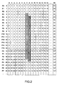
- a conventional way of storing the pixels of the image in the memories of the different PEs is to use the PEO (PE # 0) to store and process the line 0 of the image, the PE1 (PE # 1) for store and process line 1 and so on until PE15 (PE # 15) to store and process line 15. Since an image typically has more than 16 lines, the user will use PE0 to store and process lines 0, 16, 32, 48, 64, 80, ... of the image, the PE1 to store and process the lines 1, 17, 33, 49, 65, 81, ... of the image and so to PE15 for storing and processing lines 15, 31, 47, 63, 79, 95, ... of the image.
- Ad x + Lx * Int (y / Np), (Int (z) denoting the integer part of z).
- This storage is represented figure 2 .
- This figure considers the case of an image of width 64 pixels and shows a usual way to put it on a SIMD of 16 PEs organized in ring topology.
- the columns represent the columns of the image
- the lines represent the lines of the image
- the PE number is indicated at the extreme left of each line
- the address where each pixel is arranged is indicated at inside each box.
- the boundaries between homogeneous address areas are represented by black lines.
- the PE which is in charge of storing the result pixel must fetch the operands it needs to perform its calculations not only in memories and / or registers belonging to it but also in memories and / or registers that belong to neighboring PEs, or even neighbors of neighbors, or even further.
- I (x, y) be the pixels of the original image.
- R (x, y + 64) be the pixels of the result image.
- R ⁇ x , there + 64 at ⁇ - 1 , - 1 * l ⁇ x - 1 , there - 1 + at ⁇ 0 , - 1 * l ⁇ x , there - 1 + at ⁇ 1 , - 1 * l ⁇ x + 1 , there - 1 + at ⁇ - 1 , 0 * l ⁇ x - 1 , there + at 0 0 * l x there + at 1 0 * l ⁇ x + 1 , there + at ⁇ - 1 , 1 * l ⁇ x - 1 , there + 1 + at 0 1 * l ⁇ x , there + 1 + at 0 1 * l ⁇ x , there + 1 + at 0 1 * l ⁇ x , there + 1 + at 0 1 * l ⁇ x , there + 1 + at 1 1 ) * l ⁇ x + 1 , there + 1 .
- Each of the 16 pixels read is multiplied by the first coefficient of the convolution mask.
- Each of the 16 pixels read is multiplied by the 2nd coefficient of the convolution mask and the result of this 2nd multiplication is added to the result of the 1st multiplication. And so on for the 9 coefficients of the convolution mask. (9 coefficients because we took the example of a convolution 3x3).
- the first operation is then completed. There are then 31 similar operations to process the remaining 31 columns of the upper half of the square to be processed and then 32 similar operations to process the 32 columns of the lower half of this square.
- the example chosen concerns a rectangle whose edges are not aligned on the boundaries between homogeneous address areas, that is to say a rectangle whose upper edge has an ordinate which is not a multiple of the number of PEs.
- This objection does not stand up to analysis.
- the case of having to deal with such rectangles is a frequent case in image processing.
- the rectangle containing the result image had edges aligned on the boundaries between homogeneous address areas, it would nevertheless be necessary, to treat the different steps of a 3x3 convolution to look like operands of the vertical segments 16x1. whose ends would not all be aligned on the boundaries between homogeneous address areas.
- a 1st technique is a loading in 2 times with a conditional activation of the PEs.
- a first step only PEs to read at address 7 actually perform the read operation.
- a second step only the PEs to be read at the address 71 actually perform the read operation. It is therefore the programmer of the application that must manage the fact that, to achieve this first step, some PEs must load as operand a pixel they have stored at address 7 while other PEs must load as operand a pixel they have stored at address 71.
- some PEs must load as operand a pixel they have stored at address 7 while other PEs must load as operand a pixel they have stored at address 71.
- an important difficulty to program this type of machine But also a lower efficiency of execution due to the surplus of instructions to be executed.
- a second technique is the establishment of an indirection register within each PE.
- An indirection register is a register which allows access to a word whose address is contained in this register. Thanks to this indirection register, each PE can calculate an address of its own, load it into the indirection register and use it to access its own memory. But, as for the 1 st technique, one finds on the one hand an additional difficulty of programming since it is the programmer of application which must manage the difficulty and on the other hand a less efficiency of execution due to the surplus of instructions to execute.
- the difficulty is even greater if we use a SIMD organized according to a two-dimensional topology.
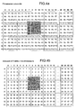
- the figures 4 use the same example of an image of width 64 pixels but uses a SIMD of 16 PEs organized in 4x4 torus topology.
- the pixels to be read are no longer stored at 2 different addresses as before but at 4 different addresses: address 1 for the PE15, address 2 for the PEs 12, 13, 14, address 17 for the PEs 3, 7, 11, address 18 for other PEs.
- the difficulty still grows if we use a SIMD organized according to a multidimensional topology.
- the pixels to be read are stored at 8 different addresses in three-dimensional topology and at 16 different addresses in four-dimensional topology. Except in special cases (particular position of the zone to be read or written) where the number of different addresses is lower.
- the object of the invention is to overcome these disadvantages.
- the invention is based on the fact that the instruction, instead of defining all the readings and / or all the writes of the elementary processors by indicating the address at which each elementary processor reads or writes in its own memory , defines the set of reads and / or the set of writes of the elementary processors each in his own memory as a reading and / or writing on a field of action.
- the set of memory words of all the elementary processors is seen as a single data structure of the N-dimensional array type, this array possibly representing a signal (dimension 1) or an image (dimension 2) or a volume (dimension 3) or ...
- the action field is defined by the instruction, by reference to this data structure and as a subset of this data structure.
- field of action we mean a set of memory words due to a memory word per elementary processor, this memory word being located in the memory of the elementary processor, a field of action of an operand being the set of memory words read by the elementary processors each in its own memory to acquire this operand, a field of action of a result being the set of memory words written by the elementary processors each in its own memory to store this result.
- the instruction comprises for each operand and / or each result, information relating to the position of this field of action, this position being defined as being a position within a single data structure of the N-dimensional array type ( signal or image or volume or ...), distributed over the memories of the various elementary processors, N being an integer equal to or greater than 1.
- the term data structure denotes this unique data structure of the array type. dimension N.
- the position of the action field makes it possible to calculate the address at which each elementary processor must read in its own memory the memory word which concerns it in the operand and / or write in its own memory the memory word which concerns it in the memory. result.
- a typical instruction on a modern HMIS requires all PEs or some of them to perform the same operation for all, dealing with multiple operands and storing the result in one or more locations.
- the instruction defines for each operand and for each result, the address where the different PEs will read the operand or store the result.
- a conventional SIMD can only take into account action fields corresponding to homogeneous addressing areas.
- a parallel processor designed according to the invention allows the different operands or results of an instruction to take into account action fields that do not necessarily correspond to homogeneous address areas.
- the subject of the invention is a parallel processor which comprises elementary processors PE each comprising at least one computing unit and at least one memory which comprises memory words, and arranged according to a topology, with a determined position within this topology and able to execute simultaneously the same instruction on different data, the instruction comprising the reading of at least one operand and / or comprising the writing of at least one result.
- elementary processors PE each comprising at least one computing unit and at least one memory which comprises memory words, and arranged according to a topology, with a determined position within this topology and able to execute simultaneously the same instruction on different data, the instruction comprising the reading of at least one operand and / or comprising the writing of at least one result.
- the instruction defines the set of readings and / or the set of writes of the elementary processors each in its own memory as a reading and / or a writing on a field of action, a field of action being a set of memory words with one memory word per elementary processor, this memory word being located in the memory of the elementary processor, a field of action of an operand being the set of memory words read by the elementary processors each in its own memory to acquire this operand, a field of action of a result being set of memory words written by the elementary processors each in its own memory for storing this result, in that the instruction comprises for each operand and / or each result, information relating to the position of this field of action, in that the position of the field of action is defined as being a position within a single data structure of array type of dimension N, where N is an integer equal to or greater than 1, in that this array is distributed over the memories of the different elementary processors.
- the proposed parallel processor implements the following principle: for each operand and for each element of the data structure where to store the result, the instruction does not define the address at which the PE must read the operand or write the result , but information allowing to define the position of the field of action of the operand or the result within the structure of data. With this information and a value related to the position of each PE, calculating means allow each PE to know the address at which it must read the operand or write the result.
- the position of the field of action is defined much more flexibly than on a conventional SIMD.
- a parallel processor makes it possible to take into account fields of action such as those mentioned in the example of the image processing and illustrated by the figures 2 , 3 and 4 ; and this although the cells that make up these fields of action are at different addresses according to the PEs.
- the parallel processor comprises means for calculating the position of the field of action as a function of said information, related to the means for calculating the address.
- the means for calculating the address within each elementary processor as a function of the position of the field of action can be either fully localized at the level of each elementary processor, either partially localized at each elementary processor and partially grouped between several elementary processors.
- the elementary processors are arranged according to a P-dimensional topology, P being an integer greater than or equal to 1 and / or the data to be processed belong to a structure in an N-dimensional space, N being an integer greater than or equal to to 1.
- the calculation of the address of the element of the data structure which concerns an elementary processor of abscissa p according to said dimension is obtained by combining a value related to the position of the field and a value related to the position of the elementary processor.
- the field of action having ends defined by its coordinates
- the position of the field of action is for example defined by the position of the end whose coordinates are minimal.
- the parallel processor is for example SIMD type.
- the instruction defines not the address at which each PE must read an operand or write a result but information on the position of the field of action within the processed data structure. This position can be defined either in absolute value or in relative value with respect to a previous position. A number of calculation steps are therefore necessary to deduce an address specific to each PE.
- a first step consists in calculating the position of the action field from the instruction in progress if it is not defined in absolute value by the instruction. At the end of this first stage, the result is independent of the EP.
- a second step is to calculate the address at which each PE must read an operand or write a result from the position of the field Action.
- the address is obtained by addition or subtraction of a value related to the position of the field and a value related to the position of the PE.
- the result depends on the PE.
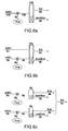
- an illustrated implementation figure 5 may consist in calculating the position of the field of action centrally by the computing means 50 while each PE uses this information to deduce an address Ad in its set of memories and / or registers; this address is obtained by the address calculation means 41, 42, 43 of each PE.
- the advantage of this principle is to minimize the volume of calculations to be performed in each PE and therefore the volume of hardware.
- Another implementation can consist in calculating everything at the level of each PE: the position of the field of action and the corresponding address.
- the disadvantage of this variant is to increase the volume of calculations to be performed in each PE and therefore the volume of hardware. However, it can reduce the amount of information to be transmitted to all PEs and therefore the number of wires on the circuit, which can be interesting in some cases.
- each PE can be done by means of a hard-wired hardware or a more flexible hardware, for example a programmable processor.
- the calculations can also be done in pure software by the ALUs of the PEs, thus without adding additional hardware, provided that each PE has a register indirection. Such an implementation, even more economical in hardware, can be interesting in some applications.
- the information defining the position of the field of action For example the center of the field or an end in a direction defined in advance. As all these choices are equivalent to a translation and that the passage from one to the other is trivial, we will not extend more on this point. In fact, these choices have in common the fact that the position of the field of action is defined by the position of a centroid obtained by linear combination of the ends, the sum of the weights of the ends being equal to 1.
- the information chosen to define the position of an action field is the point of the field of which all the coordinates are minimal. In other words, the end of the field in the direction of the point at infinity worth - ⁇ on each coordinate.
- the coordinate point (7, 3) for the 1 st step of the 1 st operation On the figures 2 , 3 and 4 , the coordinate point (7, 3) for the 1 st step of the 1 st operation.
- the invention can be applied to parallel processors organized in mono, bi, tri or multidimensional topologies and, in each of these topologies, on mono dimensional (eg signal), two dimensional (eg image) and three dimensional ( eg 3D volume for the resolution of partial differential equations) or multidimensional, but also for different storage modes of each data structure on each type of parallel processor.
- mono dimensional eg signal
- two dimensional eg image
- three dimensional eg 3D volume for the resolution of partial differential equations
- multidimensional eg 3D volume for the resolution of partial differential equations
- the invention can also be applied to processing architectures involving a large number of elementary processors performing the same processing on different data, including if this architecture does not fall into the category of SIMD. For example, if the control structure is not a sequencer or is not programmable or if the programming is done at a higher level than an instruction.
- the first exemplary embodiment relates to the case of a mono-dimensional parallel processor, for example a ring and a mono-dimensional data structure, for example a signal.
- Np being the number of PEs.
- the set of PEs is seen as a segment of width Np and the field of action is a segment of width Np: it contains Np elements.
- This equation can give rise to many implementations, ranging from pure hardware to pure software.
- This type of implementation which is particularly simple, can be transposed on all the exemplary embodiments that will be described. More generally, it can be transposed on any type of parallel processor organized in mono, bi, tri or multidimensional topologies and, in each of these topologies, on mono (ex: signal), bi (ex: image), data structures. sort (them: 3D volume) or multidimensional. In fact, it suffices to resume the calculation according to the type of parallel processor, the data structure and the storage chosen then adapt the implementation accordingly.
- the second embodiment relates to the case of a mono-dimensional parallel processor for example a ring and a two-dimensional data structure, for example an image.
- Np be the number of PEs
- Lx the width of the image to be processed, ie the number of pixels on each line and Ly its height, ie the number of pixels on each column. It is more exactly the upper bounds for the numbers of PEs, pixels on each line and each column. Indeed, in most cases and for purposes of hardware simplification, it is preferred to plunge the image to be processed in a larger image and thus choose Lx and Ly values greater than the dimensions of the image to be processed. On the one hand, if several images of different sizes are to be processed, it may be preferable to make a single choice for treating the larger of them. On the other hand, to simplify the implementation when it is hardware, we often choose a power of 2.
- This type of storage used figure 3 is to consider the set of PEs as a horizontal block of PEs, each PE being responsible for a column or columns. It differs from the one previously analyzed and represented by figure 2 which amounts to considering the set of PEs as a vertical block of PEs, each PE being responsible for one line or several lines.
- write for each pixel (x, y): w there + Ly * x
- the field of action is a horizontal segment of width Np.
- the third embodiment is the case of a mono-dimensional parallel processor (for example a ring) and a data structure of dimension greater than 2.
- Lx be the width of the volume to be treated and Ly its depth and Lz its height, or more exactly, for the reasons we have seen previously, upper bounds of these 3 quantities.
- the set of PEs is seen as a horizontal segment of width Np and the field of action is a horizontal segment of width Np.
- the fourth embodiment is the case of a two-dimensional parallel processor for example a torus and a two-dimensional data structure for example an image.
- Nx be the number of PEs on the x-axis, Ny the number of PEs on the y-axis and hence Nx * Ny the total number of PEs.
- Lx be the width of the image to be processed and Ly its height, or as we have seen previously, upper bounds of these 2 quantities.
- Lx and Ly are respectively chosen from the multiples of Nx and Ny.
- (px, py) the PE of coordinates (px, py) on the torus of PEs.
- the set of PEs is seen as a rectangle of width Nx and height Ny and the field of action is a rectangle of width Nx and height Ny.
- this storage is modeled on the storage used for a single-dimensional data structure. In fact, it reproduces this arrangement in each of the 2 directions of space.
- the treatment device will be exactly the same, but must be applied in each of the 2 directions of space.
- Adx Int ⁇ Xmin + nx - 1 - px / nx
- Ad Adx + (Lx / Nx) * Ady, which amounts to concatenating the low-weight Adx represented on LLx-LNx bits and the most significant Ady represented on LLy-LNy bits.
- the proposed principle can be applied to parallel processors organized in mono, bi, tri or multidimensional topologies and, in each of these topologies, on mono, bi, tri or multidimensional data structures.
- n be the dimension of the data structure and p the dimension of the topology of the parallel processor.
- n n ⁇ p
- we increase the dimension of the structure by choosing one axis, (then another, then another, ..., until we obtain a structure of dimension p) and we cut this axis in slices in order to to split it.
- This extension is totally independent of the extension mentioned in the previous paragraph; it can be coupled to it. It therefore applies to the multidimensional case, both for the topology of the parallel processor and for the data structure. Just apply it in each dimension. Consequently, the method applies to any storage mode in which a parallelepiped of size Lx on the x-axis, Ly on the y-axis, ... is conserved and processed by the same PE, whereas Neighboring PEs (for the parallel processor topology) store and process neighboring parallelepipeds (for the topology of the data structure).
Landscapes
- Engineering & Computer Science (AREA)
- Theoretical Computer Science (AREA)
- Software Systems (AREA)
- Physics & Mathematics (AREA)
- General Engineering & Computer Science (AREA)
- General Physics & Mathematics (AREA)
- Computer Hardware Design (AREA)
- Computing Systems (AREA)
- Image Processing (AREA)
- Multi Processors (AREA)
- Image Input (AREA)
Claims (22)
- Parallelprozessor, der Elementarprozessoren (3) umfasst, die jeweils wenigstens eine Recheneinheit und wenigstens einen Speicher umfassen, der Speicherwörter umfasst, und die gemäß einer Topologie angeordnet sind, mit einer vorbestimmten Position im Innern dieser Topologie und so ausgelegt, dass sie gleichzeitig denselben Befehl an verschiedenen Daten ausführen können, wobei der Befehl das Lesen von wenigstens einem Operanden und/oder das Schreiben von wenigstens einem Ergebnis beinhaltet, dadurch gekennzeichnet, dass der Befehl alle Lese- und/oder Schreibvorgänge der Elementarprozessoren jeweils in ihrem eigenen Speicher als Lesen und/oder Schreiben auf ein Aktionsfeld definiert, wobei ein Aktionsfeld ein Satz von Speicherwörtern aufgrund eines Speicherworts pro Elementarprozessor ist, wobei sich dieses Speicherwort im Speicher des Elementarprozessors befindet, wobei ein Aktionsfeld eines Operanden das Ganze der Speicherwörtern ist, die von den Elementarprozessoren jeweils in ihrem eigenen Speicher gelesen wurden, um diesen Operanden zu erfassen, wobei ein Aktionsfeld eines Ergebnisses das Ganze der Speicherwörtern ist, die von den Elementarprozessoren jeweils in ihrem eigenen Speicher geschrieben wurden, um dieses Ergebnis zu speichern, und dadurch, dass der Befehl für jeden Operanden und/oder jedes Ergebnis Informationen in Bezug auf die Position des Aktionsfeldes umfasst, und dadurch, dass die Position des Aktionsfeldes als eine Position im Innern einer eindeutigen Datenstruktur des Tabellentyps mit Dimension N ist, wobei N eine ganze Zahl gleich oder größer als 1 ist, dadurch, dass diese Tabelle auf die Speicher der verschiedenen Elementarprozessoren verteilt ist, und dadurch, dass der Parallelprozessor Mittel zum Berechnen der Adresse jedes Operanden und/oder jedes Ergebnisses im Innern jedes Elementarprozessors in Abhängigkeit von der Position des Aktionsfeldes und der Position des Elementarprozessors im Innern der Topologie umfasst.
- Parallelprozessor nach dem vorherigen Anspruch, dadurch gekennzeichnet, dass er Mittel (50) zum Berechnen der Position des Aktionsfelds in Abhängigkeit von den Informationen umfasst, die mit den Mitteln zum Berechnen der Adresse verbunden sind.
- Parallelprozessor nach einem der vorherigen Ansprüche, dadurch gekennzeichnet, dass sich die Mittel (41, 42, 43) zum Berechnen der Adresse im Innern jedes Elementarprozessors an jedem Elementarprozessor befinden.
- Parallelprozessor nach dem vorherigen Anspruch, dadurch gekennzeichnet, dass sich die Mittel (41, 42, 43) zum Berechnen der Adresse im Innern jedes Elementarprozessors an der Recheneinheit (31) jedes Elementarprozessors befinden.
- Parallelprozessor nach einem der vorherigen Ansprüche, dadurch gekennzeichnet, dass sich die Mittel zum Berechnen der Adresse im Innern jedes Elementarprozessors zum Teil an jedem Elementarprozessor und zum Teil zwischen mehreren Elementarprozessoren gruppiert befinden.
- Parallelprozessor nach einem der vorherigen Ansprüche in Kombination mit Anspruch 2, dadurch gekennzeichnet, dass die Mittel zum Berechnen der Position des Aktionsfeldes Folgendes sind:- allen Elementarprozessoren gemeinsam, oder- ganz oder teilweise an den Mitteln zum Berechnen der Adresse der Daten positioniert.
- Parallelprozessor nach einem der vorherigen Ansprüche, dadurch gekennzeichnet, dass die Elementarprozessoren gemäß einer Topologie mit P Dimensionen angeordnet sind, wobei P eine ganze Zahl gleich oder größer als 1 ist.
- Parallelprozessor nach einem der vorherigen Ansprüche, dadurch gekennzeichnet, dass, da die Elementarprozessoren gemäß einer Topologie mit wenigstens einer Dimension angeordnet sind, für jede Dimension die Mittel zum Berechnen der Adresse des Elements der Datenstruktur, die einen Elementarprozessor von Abszisse P gemäß der Dimension betrifft, durch Kombinieren eines mit der Position des Feldes verbundenen Wertes und eines mit der Position des Elementarprozessors verbundenen Wertes erhalten werden.
- Parallelprozessor nach einem der vorherigen Ansprüche, dadurch gekennzeichnet, dass, da das Aktionsfeld durch ihre Koordinaten definierte Enden aufweist, die Position des Aktionsfelds durch die Position eines Baryzentrums definiert wird, das durch lineares Kombinieren seiner Enden erhalten wird, wobei die Summe der Wertigkeiten der Enden gleich 1 ist.
- Parallelprozessor nach einem der vorherigen Ansprüche, dadurch gekennzeichnet, dass, da das Aktionsfeld durch ihre Koordinaten definierte Enden aufweist, die Position des Aktionsfelds durch die Position des Endes definiert wird, dessen Koordinaten minimal sind.
- Parallelprozessor nach dem vorherigen Anspruch, dadurch gekennzeichnet, dass, da die Prozessoren gemäß einer Topologie mit wenigstens einer Dimension angeordnet sind, für jede Dimension die Mittel zum Berechnen der Adresse des Elementes der Datenstruktur, die einen EP von Abszisse p gemäß der Dimension betreffen, Mittel zum Berechnen von Folgendem umfassen:

wobei Np die Zahl der Elementarprozessoren ist, die auf der Dimension betrachtet werden, wobei Wmin auf der Dimension in Abhängigkeit von den Koordinaten der Position definiert wird. - Parallelprozessor nach dem vorherigen Anspruch, dadurch gekennzeichnet, dass die Prozessoren gemäß einer Topologie mit einer Dimension angeordnet sind und die Datenstruktur eindimensional ist, und dadurch, dass die Position des Aktionsfelds durch Xmin und Wmin = Xmin definiert wird.
- Parallelprozessor nach dem vorherigen Anspruch, dadurch gekennzeichnet, dass, da Np eine Zweierpotenz ist, die Mittel zum Berechnen von Ad Mittel umfassen zum:- Addieren von Xmin und (Np - 1 - p),- Löschen der LNp letzten Bits des Ergebnisses, wobei LNp der Logarithmus mit Basis 2 von Np ist.
- Parallelprozessor nach Anspruch 10, dadurch gekennzeichnet, dass die Prozessoren gemäß einer Topologie mit einer Dimension angeordnet sind und die Datenstruktur zweidimensional ist, definiert in Abhängigkeit von X und Y, wobei die Dimension der Struktur gemäß X kleiner als ein vorbestimmter Wert Lx ist, und dadurch, dass die Position des Aktionsfeldes durch Xmin, Ymin und Wmin = Xmin + Lx * Ymin, definiert ist.
- Parallelprozessor nach dem vorherigen Anspruch, dadurch gekennzeichnet, dass, da Np und Lx Zweierpotenzen sind, die Mittel zum Berechnen von Ad Mittel beinhalten zum:- Addieren von Xmin und (Np - 1 - p),- Löschen der LNp letzten Bits des Ergebnisses, wobei LNp der Logarithmus mit Basis 2 von Np ist,- niederwertiges Verketten der vorherigen Menge, die auf LLx-LNp Bits repräsentiert wird, und hochwertiges Verketten von Ymin, wobei LLx der Logarithmus mit Basis 2 von Lx ist.
- Parallelprozessor nach Anspruch 10, dadurch gekennzeichnet, dass die Prozessoren gemäß einer Topologie mit einer Dimension angeordnet sind und die Datenstruktur dreidimensional ist, definiert in Abhängigkeit von X, Y und Z, wobei die Dimensionen der Struktur gemäß X und Y jeweils kleiner als vorbestimmte Werte Lx und Ly sind, und dadurch, dass die Position des Aktionsfelds durch Xmin, Ymin, Zmin und Wmin = Xmin + Lx * (Ymin + Ly * Zmin) definiert ist.
- Parallelprozessor nach dem vorherigen Anspruch, dadurch gekennzeichnet, dass, da Np, Lx und Ly Zweierpotenzen sind, die Mittel zum Berechnen von Ad Mittel umfassen zum:- Addieren von Xmin und (Np - 1 - p),- Löschen der LNp letzten Bits des Ergebnisses, wobei LNp der Logarithmus mit Basis 2 von Np ist,- niederwertiges Verketten der vorherigen Menge, die auf LLx-LNp Bits repräsentiert ist, mittelwertiges Verketten von Ymin, das auf Ly Bits repräsentiert ist, und hochwertiges Verketten von Zmin, das auf Lz Bits repräsentiert ist, wobei LLx der Logarithmus mit Basis 2 von Lx ist.
- Parallelprozessor nach Anspruch 10, dadurch gekennzeichnet, dass die Prozessoren gemäß einer Topologie mit einer Dimension angeordnet sind und die Datenstruktur vier Dimensionen hat, definiert in Abhängigkeit von X, Y, Z und T, wobei die Dimensionen der Struktur gemäß X, Y und Z jeweils kleiner als vorbestimmte Werte Lx, Ly und Lz sind, und dadurch, dass die Position des Aktionsfeldes durch Xmin, Ymin, Zmin, Tmin und Wmin = Xmin + Lx * (Ymin + Ly * (Zmin + Lz * Tmin)) definiert ist.
- Parallelprozessor nach Anspruch 10, dadurch gekennzeichnet, dass die Prozessoren gemäß einer Topologie mit zwei Dimensionen angeordnet sind und jeweils Nx und Ny Prozessoren gemäß der einen und der anderen Dimension umfassen, die Datenstruktur zweidimensional ist, definiert in Abhängigkeit von X und Y, die Dimension der Struktur gemäß X kleiner als ein vorbestimmter Wert Lx ist, und dadurch, dass die Position des Aktionsfeldes durch Xmin, Ymin definiert ist, und- die Adresse Adx des Elementes, das den EP Nr. px betrifft, der gemäß X im Innern des Feldes betrachtet wird, mit der folgenden Formel erhalten wird:
 - und die Adresse Ady des Elementes, das den EP Nr. py betrifft, der gemäß Y im Innern des Feldes betrachtet wird, mit der folgenden Formel erhalten wird:
- Parallelprozessor nach dem vorherigen Anspruch, dadurch gekennzeichnet, dass, da Nx, Ny, Lx und Ly Zweierpotenzen sind, wobei LLx und LLy jeweils der Logarithmus mit Basis 2 von Lx und Ly sind, die Mittel zum Berechnen von Ad Mittel umfassen zum:- Addieren von Xmin und (Nx-1-px),- Löschen der LNx letzten Bits des Ergebnisses, wobei LNx der Logarithmus mit Basis 2 von Nx ist, daher wird Adx auf LLx-LNx Bits erhalten,- Addieren von Ymin und (Ny-1-py),- Löschen der LNy letzten Bits des Ergebnisses, wobei LNy der Logarithmus mit Basis 2 von Ny ist, daher wird Ady auf LLy-LNy Bits erhalten,- niederwertiges Verketten von Adx, das auf LLx-LNx Bits repräsentiert ist, und hochwertiges Verketten von Ady, das auf LLy-LNy Bits repräsentiert ist.
- Parallelprozessor nach Anspruch 10, dadurch gekennzeichnet, dass die Prozessoren gemäß einer Topologie mit wenigstens drei Dimensionen angeordnet sind und jeweils Nx, Ny, Nz, ... Prozessoren gemäß jeder Dimension umfassen, die Datenstruktur auf wenigstens drei Dimensionen in Abhängigkeit von X, Y, Z, ... definiert ist, die Dimension der Struktur gemäß jeder der Dimensionen kleiner als ein vorbestimmter Wert Lx, Ly, Lz, ... ist und, da Nx, Ny, Nz, ..., Lx, Ly, Lz, ... Zweierpotenzen sind, wobei LLx, LLy, LLz, ... Logarithmen mit Basis 2 von Lx, Ly, Lz, ... sind, die Mittel zum Berechnen von Ad Mittel umfassen zum:- Verketten auf einem einzigen Wort von LLx + LLy + LLz + ... Bits der verschiedenen Koordinaten des zum Definieren der Position des Feldes verwendeten Punkts; man erhält w,- Vertauschen der Reihenfolge der Bits von w; d.h. es wird das Wort w' erhalten;- Unterteilen von w' in Wörter der Größe LLx, LLy, LLz, ... Bits; d.h. es werden die Wörter wx', wy', wz', ... erhalten,- in jeder der Dimensionen Anwenden von Folgendem:i. Hinzufügen von (Nx - 1 - px) zu wx',ii. Löschen der LNx letzten Bits des Ergebnisses; man erhält Adx,',iii. Hinzufügen von (Ny - 1 - py) zu wy',iv. Löschen der LNy letzten Bits des Ergebnisses; man erhält Ady',v. usw. in jeder Richtung,- erneutes Vertauschen der Reihenfolge der Bits von Adx', Ady', Adz', ...; man erhält somit die Anordnungsadressen Adx, Ady, Adz in jeder Richtung,- Verketten dieser Adressen zu einem einzigen Wort Ad, das die das Feld im Innern jedes EP betroffene Adresse repräsentiert.
- Parallelprozessor nach einem der vorherigen Ansprüche, dadurch gekennzeichnet, dass der Parallelprozessor ein Rechner des SIMD-Typs ist.
Applications Claiming Priority (2)
| Application Number | Priority Date | Filing Date | Title |
|---|---|---|---|
| FR0704574A FR2918190B1 (fr) | 2007-06-26 | 2007-06-26 | Dispositif d'adressage pour processeur parallele. |
| PCT/EP2008/058141 WO2009000880A1 (fr) | 2007-06-26 | 2008-06-26 | Dispositif d'adressage pour processeur parallele |
Publications (2)
| Publication Number | Publication Date |
|---|---|
| EP2162829A1 EP2162829A1 (de) | 2010-03-17 |
| EP2162829B1 true EP2162829B1 (de) | 2012-08-15 |
Family
ID=38926388
Family Applications (1)
| Application Number | Title | Priority Date | Filing Date |
|---|---|---|---|
| EP08774325A Active EP2162829B1 (de) | 2007-06-26 | 2008-06-26 | Adressierungsvorrichtung für parallelprozessor |
Country Status (8)
| Country | Link |
|---|---|
| US (1) | US10789072B2 (de) |
| EP (1) | EP2162829B1 (de) |
| JP (1) | JP5608932B2 (de) |
| KR (1) | KR101547366B1 (de) |
| ES (1) | ES2391690T3 (de) |
| FR (1) | FR2918190B1 (de) |
| IL (1) | IL202715A (de) |
| WO (1) | WO2009000880A1 (de) |
Families Citing this family (3)
| Publication number | Priority date | Publication date | Assignee | Title |
|---|---|---|---|---|
| JP5739779B2 (ja) * | 2011-09-26 | 2015-06-24 | ルネサスエレクトロニクス株式会社 | Simdプロセッサ及びコントロールプロセッサ並びにプロセッサ要素 |
| GB2536211B (en) * | 2015-03-04 | 2021-06-16 | Advanced Risc Mach Ltd | An apparatus and method for executing a plurality of threads |
| US11281554B2 (en) * | 2020-03-17 | 2022-03-22 | Samsung Electronics Co., Ltd. | System and method for in-memory computation |
Family Cites Families (11)
| Publication number | Priority date | Publication date | Assignee | Title |
|---|---|---|---|---|
| WO1991010200A1 (en) * | 1990-01-05 | 1991-07-11 | Maspar Computer Corporation | Parallel processor memory system |
| JPH05290188A (ja) * | 1992-04-15 | 1993-11-05 | Fujitsu Ltd | 超並列計算機 |
| IT1288076B1 (it) | 1996-05-30 | 1998-09-10 | Antonio Esposito | Multicalcolatore elettronico numerico parallelo multiprocessore a ridondanza di processori accoppiati |
| JP3767085B2 (ja) * | 1996-09-04 | 2006-04-19 | セイコーエプソン株式会社 | 情報処理回路及びマイクロコンピュータ |
| US6105125A (en) * | 1997-11-12 | 2000-08-15 | National Semiconductor Corporation | High speed, scalable microcode based instruction decoder for processors using split microROM access, dynamic generic microinstructions, and microcode with predecoded instruction information |
| US6834295B2 (en) * | 2000-02-24 | 2004-12-21 | Pts Corporation | Methods and apparatus for providing bit-reversal and multicast functions utilizing DMA controller |
| US6665790B1 (en) * | 2000-02-29 | 2003-12-16 | International Business Machines Corporation | Vector register file with arbitrary vector addressing |
| JP2004234407A (ja) * | 2003-01-31 | 2004-08-19 | Hitachi Ulsi Systems Co Ltd | データ処理装置 |
| GB2417105B (en) * | 2004-08-13 | 2008-04-09 | Clearspeed Technology Plc | Processor memory system |
| GB0420004D0 (en) * | 2004-09-09 | 2004-10-13 | Koninkl Philips Electronics Nv | Interconnections in SIMD processor architectures |
| GB2437836B (en) * | 2005-02-25 | 2009-01-14 | Clearspeed Technology Plc | Microprocessor architectures |
-
2007
- 2007-06-26 FR FR0704574A patent/FR2918190B1/fr not_active Expired - Fee Related
-
2008
- 2008-06-26 ES ES08774325T patent/ES2391690T3/es active Active
- 2008-06-26 WO PCT/EP2008/058141 patent/WO2009000880A1/fr not_active Ceased
- 2008-06-26 KR KR1020097027117A patent/KR101547366B1/ko not_active Expired - Fee Related
- 2008-06-26 JP JP2010513919A patent/JP5608932B2/ja not_active Expired - Fee Related
- 2008-06-26 US US12/666,551 patent/US10789072B2/en active Active
- 2008-06-26 EP EP08774325A patent/EP2162829B1/de active Active
-
2009
- 2009-12-14 IL IL202715A patent/IL202715A/en active IP Right Grant
Also Published As
| Publication number | Publication date |
|---|---|
| IL202715A (en) | 2014-12-31 |
| US20100250897A1 (en) | 2010-09-30 |
| US10789072B2 (en) | 2020-09-29 |
| EP2162829A1 (de) | 2010-03-17 |
| JP2010531502A (ja) | 2010-09-24 |
| KR101547366B1 (ko) | 2015-08-25 |
| JP5608932B2 (ja) | 2014-10-22 |
| FR2918190A1 (fr) | 2009-01-02 |
| WO2009000880A1 (fr) | 2008-12-31 |
| IL202715A0 (en) | 2010-06-30 |
| KR20100033979A (ko) | 2010-03-31 |
| FR2918190B1 (fr) | 2009-09-18 |
| ES2391690T3 (es) | 2012-11-29 |
Similar Documents
| Publication | Publication Date | Title |
|---|---|---|
| JP7132824B2 (ja) | ニューラルネットワークにおいてデコンボルーション演算を実行する装置及びその方法 | |
| EP3844679B1 (de) | Architektur eines computers zur berechnung einer faltungsschicht in einem neuralen faltungsnetzwerk | |
| KR102452951B1 (ko) | 뉴럴 네트워크의 컨볼루션 연산을 수행하는 방법 및 장치 | |
| FR2714505A1 (fr) | Dispositif et procédé pour générer une image destinée à un traitement graphique d'ordinateur tridimensionnel. | |
| FR2542470A1 (fr) | Systeme de machine a calculer a multiprocesseur pour convertir des elements-objets definis dans une structure de donnees hierarchique en une representation visuelle coloree | |
| US12361571B2 (en) | Method and apparatus with convolution neural network processing using shared operand | |
| FR2996037A1 (fr) | Moteur hybride pour processeur central et processeur graphique | |
| EP2162829B1 (de) | Adressierungsvorrichtung für parallelprozessor | |
| EP1368747A1 (de) | Verfahren und vorrichtung zur verkürzung der rechenzeit eines produktes, einer multiplikation und einer potenzierung nach der montgomery-methode | |
| CN111507456B (zh) | 具有卷积神经网络处理的方法和装置 | |
| EP0780775B1 (de) | Architektur eines Systems von Arrayprozessoren mit parallelen Mehrfachstrukturen | |
| FR3144687A1 (fr) | Architecture de réseau neuronal pour un réseau systolique de processeurs et procédé de traitement de données utilisant un réseau neuronal | |
| CN119110958A (zh) | 图像处理设备及其操作方法 | |
| EP4242855B1 (de) | Adressengenerator für einen rechner mit einzelbefehl-mehrdatenarchitektur | |
| JP3860545B2 (ja) | 画像処理装置及び画像処理方法 | |
| EP3814893A1 (de) | Prozessorspeicherzugriff | |
| EP0329572B1 (de) | Binärzahlmultiplizierer mit einer sehr grossen Bitzahl | |
| Letellier | Real time image synthesis on a SIMD linear array processor: algorithms and architectures | |
| EP2192555B1 (de) | Display of parameterised data | |
| Jiang | Review of" Image processing and analysis: variational, PDE, Wavelet, and Stochastic methods" by Tony F. Chan and Jianhong (Jackie) Shen | |
| FR2539529A1 (fr) | Procede pour le traitement d'informations binaires et processeur pour la mise en oeuvre de ce procede | |
| FR2650088A1 (fr) | Procede pour la generation de schemas logiques de circuits multiplieurs parametrables a decodeur de booth au moyen d'un ordinateur et circuits multiplieurs correspondants | |
| WO2006042976A1 (fr) | Procede de construction d’une forme bidimensionnelle a partir d’une forme tridimensionnelle | |
| WO2004100065A2 (fr) | Systeme et procede de simulation de l’evolution d’organismes vivants complexes | |
| WO2003093973A1 (fr) | Multiplication au sens de montgomery |
Legal Events
| Date | Code | Title | Description |
|---|---|---|---|
| PUAI | Public reference made under article 153(3) epc to a published international application that has entered the european phase |
Free format text: ORIGINAL CODE: 0009012 |
|
| 17P | Request for examination filed |
Effective date: 20091208 |
|
| AK | Designated contracting states |
Kind code of ref document: A1 Designated state(s): AT BE BG CH CY CZ DE DK EE ES FI FR GB GR HR HU IE IS IT LI LT LU LV MC MT NL NO PL PT RO SE SI SK TR |
|
| AX | Request for extension of the european patent |
Extension state: AL BA MK RS |
|
| 17Q | First examination report despatched |
Effective date: 20100628 |
|
| DAX | Request for extension of the european patent (deleted) | ||
| GRAP | Despatch of communication of intention to grant a patent |
Free format text: ORIGINAL CODE: EPIDOSNIGR1 |
|
| GRAS | Grant fee paid |
Free format text: ORIGINAL CODE: EPIDOSNIGR3 |
|
| GRAA | (expected) grant |
Free format text: ORIGINAL CODE: 0009210 |
|
| AK | Designated contracting states |
Kind code of ref document: B1 Designated state(s): AT BE BG CH CY CZ DE DK EE ES FI FR GB GR HR HU IE IS IT LI LT LU LV MC MT NL NO PL PT RO SE SI SK TR |
|
| REG | Reference to a national code |
Ref country code: CH Ref legal event code: EP Ref country code: GB Ref legal event code: FG4D Free format text: NOT ENGLISH Ref country code: AT Ref legal event code: REF Ref document number: 571151 Country of ref document: AT Kind code of ref document: T Effective date: 20120815 |
|
| REG | Reference to a national code |
Ref country code: IE Ref legal event code: FG4D Free format text: LANGUAGE OF EP DOCUMENT: FRENCH |
|
| REG | Reference to a national code |
Ref country code: DE Ref legal event code: R096 Ref document number: 602008018063 Country of ref document: DE Effective date: 20121011 |
|
| REG | Reference to a national code |
Ref country code: ES Ref legal event code: FG2A Ref document number: 2391690 Country of ref document: ES Kind code of ref document: T3 Effective date: 20121129 |
|
| REG | Reference to a national code |
Ref country code: NL Ref legal event code: T3 |
|
| REG | Reference to a national code |
Ref country code: AT Ref legal event code: MK05 Ref document number: 571151 Country of ref document: AT Kind code of ref document: T Effective date: 20120815 |
|
| PG25 | Lapsed in a contracting state [announced via postgrant information from national office to epo] |
Ref country code: AT Free format text: LAPSE BECAUSE OF FAILURE TO SUBMIT A TRANSLATION OF THE DESCRIPTION OR TO PAY THE FEE WITHIN THE PRESCRIBED TIME-LIMIT Effective date: 20120815 Ref country code: NO Free format text: LAPSE BECAUSE OF FAILURE TO SUBMIT A TRANSLATION OF THE DESCRIPTION OR TO PAY THE FEE WITHIN THE PRESCRIBED TIME-LIMIT Effective date: 20121115 Ref country code: HR Free format text: LAPSE BECAUSE OF FAILURE TO SUBMIT A TRANSLATION OF THE DESCRIPTION OR TO PAY THE FEE WITHIN THE PRESCRIBED TIME-LIMIT Effective date: 20120815 Ref country code: IS Free format text: LAPSE BECAUSE OF FAILURE TO SUBMIT A TRANSLATION OF THE DESCRIPTION OR TO PAY THE FEE WITHIN THE PRESCRIBED TIME-LIMIT Effective date: 20121215 Ref country code: FI Free format text: LAPSE BECAUSE OF FAILURE TO SUBMIT A TRANSLATION OF THE DESCRIPTION OR TO PAY THE FEE WITHIN THE PRESCRIBED TIME-LIMIT Effective date: 20120815 Ref country code: LT Free format text: LAPSE BECAUSE OF FAILURE TO SUBMIT A TRANSLATION OF THE DESCRIPTION OR TO PAY THE FEE WITHIN THE PRESCRIBED TIME-LIMIT Effective date: 20120815 Ref country code: CY Free format text: LAPSE BECAUSE OF FAILURE TO SUBMIT A TRANSLATION OF THE DESCRIPTION OR TO PAY THE FEE WITHIN THE PRESCRIBED TIME-LIMIT Effective date: 20120815 |
|
| PG25 | Lapsed in a contracting state [announced via postgrant information from national office to epo] |
Ref country code: PT Free format text: LAPSE BECAUSE OF FAILURE TO SUBMIT A TRANSLATION OF THE DESCRIPTION OR TO PAY THE FEE WITHIN THE PRESCRIBED TIME-LIMIT Effective date: 20121217 Ref country code: SI Free format text: LAPSE BECAUSE OF FAILURE TO SUBMIT A TRANSLATION OF THE DESCRIPTION OR TO PAY THE FEE WITHIN THE PRESCRIBED TIME-LIMIT Effective date: 20120815 Ref country code: PL Free format text: LAPSE BECAUSE OF FAILURE TO SUBMIT A TRANSLATION OF THE DESCRIPTION OR TO PAY THE FEE WITHIN THE PRESCRIBED TIME-LIMIT Effective date: 20120815 Ref country code: LV Free format text: LAPSE BECAUSE OF FAILURE TO SUBMIT A TRANSLATION OF THE DESCRIPTION OR TO PAY THE FEE WITHIN THE PRESCRIBED TIME-LIMIT Effective date: 20120815 Ref country code: GR Free format text: LAPSE BECAUSE OF FAILURE TO SUBMIT A TRANSLATION OF THE DESCRIPTION OR TO PAY THE FEE WITHIN THE PRESCRIBED TIME-LIMIT Effective date: 20121116 Ref country code: SE Free format text: LAPSE BECAUSE OF FAILURE TO SUBMIT A TRANSLATION OF THE DESCRIPTION OR TO PAY THE FEE WITHIN THE PRESCRIBED TIME-LIMIT Effective date: 20120815 |
|
| PG25 | Lapsed in a contracting state [announced via postgrant information from national office to epo] |
Ref country code: RO Free format text: LAPSE BECAUSE OF FAILURE TO SUBMIT A TRANSLATION OF THE DESCRIPTION OR TO PAY THE FEE WITHIN THE PRESCRIBED TIME-LIMIT Effective date: 20120815 Ref country code: DK Free format text: LAPSE BECAUSE OF FAILURE TO SUBMIT A TRANSLATION OF THE DESCRIPTION OR TO PAY THE FEE WITHIN THE PRESCRIBED TIME-LIMIT Effective date: 20120815 Ref country code: CZ Free format text: LAPSE BECAUSE OF FAILURE TO SUBMIT A TRANSLATION OF THE DESCRIPTION OR TO PAY THE FEE WITHIN THE PRESCRIBED TIME-LIMIT Effective date: 20120815 Ref country code: EE Free format text: LAPSE BECAUSE OF FAILURE TO SUBMIT A TRANSLATION OF THE DESCRIPTION OR TO PAY THE FEE WITHIN THE PRESCRIBED TIME-LIMIT Effective date: 20120815 |
|
| PG25 | Lapsed in a contracting state [announced via postgrant information from national office to epo] |
Ref country code: SK Free format text: LAPSE BECAUSE OF FAILURE TO SUBMIT A TRANSLATION OF THE DESCRIPTION OR TO PAY THE FEE WITHIN THE PRESCRIBED TIME-LIMIT Effective date: 20120815 |
|
| PLBE | No opposition filed within time limit |
Free format text: ORIGINAL CODE: 0009261 |
|
| STAA | Information on the status of an ep patent application or granted ep patent |
Free format text: STATUS: NO OPPOSITION FILED WITHIN TIME LIMIT |
|
| 26N | No opposition filed |
Effective date: 20130516 |
|
| PG25 | Lapsed in a contracting state [announced via postgrant information from national office to epo] |
Ref country code: BG Free format text: LAPSE BECAUSE OF FAILURE TO SUBMIT A TRANSLATION OF THE DESCRIPTION OR TO PAY THE FEE WITHIN THE PRESCRIBED TIME-LIMIT Effective date: 20121115 |
|
| REG | Reference to a national code |
Ref country code: DE Ref legal event code: R097 Ref document number: 602008018063 Country of ref document: DE Effective date: 20130516 |
|
| BERE | Be: lapsed |
Owner name: THALES Effective date: 20130630 |
|
| PG25 | Lapsed in a contracting state [announced via postgrant information from national office to epo] |
Ref country code: MC Free format text: LAPSE BECAUSE OF FAILURE TO SUBMIT A TRANSLATION OF THE DESCRIPTION OR TO PAY THE FEE WITHIN THE PRESCRIBED TIME-LIMIT Effective date: 20120815 |
|
| REG | Reference to a national code |
Ref country code: CH Ref legal event code: PL |
|
| REG | Reference to a national code |
Ref country code: IE Ref legal event code: MM4A |
|
| PG25 | Lapsed in a contracting state [announced via postgrant information from national office to epo] |
Ref country code: BE Free format text: LAPSE BECAUSE OF NON-PAYMENT OF DUE FEES Effective date: 20130630 |
|
| PG25 | Lapsed in a contracting state [announced via postgrant information from national office to epo] |
Ref country code: LI Free format text: LAPSE BECAUSE OF NON-PAYMENT OF DUE FEES Effective date: 20130630 Ref country code: IE Free format text: LAPSE BECAUSE OF NON-PAYMENT OF DUE FEES Effective date: 20130626 Ref country code: CH Free format text: LAPSE BECAUSE OF NON-PAYMENT OF DUE FEES Effective date: 20130630 |
|
| PG25 | Lapsed in a contracting state [announced via postgrant information from national office to epo] |
Ref country code: MT Free format text: LAPSE BECAUSE OF FAILURE TO SUBMIT A TRANSLATION OF THE DESCRIPTION OR TO PAY THE FEE WITHIN THE PRESCRIBED TIME-LIMIT Effective date: 20120815 |
|
| PG25 | Lapsed in a contracting state [announced via postgrant information from national office to epo] |
Ref country code: TR Free format text: LAPSE BECAUSE OF FAILURE TO SUBMIT A TRANSLATION OF THE DESCRIPTION OR TO PAY THE FEE WITHIN THE PRESCRIBED TIME-LIMIT Effective date: 20120815 |
|
| PG25 | Lapsed in a contracting state [announced via postgrant information from national office to epo] |
Ref country code: HU Free format text: LAPSE BECAUSE OF FAILURE TO SUBMIT A TRANSLATION OF THE DESCRIPTION OR TO PAY THE FEE WITHIN THE PRESCRIBED TIME-LIMIT; INVALID AB INITIO Effective date: 20080626 Ref country code: LU Free format text: LAPSE BECAUSE OF NON-PAYMENT OF DUE FEES Effective date: 20130626 |
|
| REG | Reference to a national code |
Ref country code: FR Ref legal event code: PLFP Year of fee payment: 9 |
|
| REG | Reference to a national code |
Ref country code: FR Ref legal event code: PLFP Year of fee payment: 10 |
|
| REG | Reference to a national code |
Ref country code: FR Ref legal event code: PLFP Year of fee payment: 11 |
|
| P01 | Opt-out of the competence of the unified patent court (upc) registered |
Effective date: 20230529 |
|
| PGFP | Annual fee paid to national office [announced via postgrant information from national office to epo] |
Ref country code: NL Payment date: 20240527 Year of fee payment: 17 |
|
| PGFP | Annual fee paid to national office [announced via postgrant information from national office to epo] |
Ref country code: GB Payment date: 20240516 Year of fee payment: 17 |
|
| PGFP | Annual fee paid to national office [announced via postgrant information from national office to epo] |
Ref country code: DE Payment date: 20240514 Year of fee payment: 17 |
|
| PGFP | Annual fee paid to national office [announced via postgrant information from national office to epo] |
Ref country code: FR Payment date: 20240524 Year of fee payment: 17 |
|
| PGFP | Annual fee paid to national office [announced via postgrant information from national office to epo] |
Ref country code: IT Payment date: 20240530 Year of fee payment: 17 |
|
| PGFP | Annual fee paid to national office [announced via postgrant information from national office to epo] |
Ref country code: ES Payment date: 20240704 Year of fee payment: 17 |
|
| REG | Reference to a national code |
Ref country code: DE Ref legal event code: R119 Ref document number: 602008018063 Country of ref document: DE |
|
| REG | Reference to a national code |
Ref country code: NL Ref legal event code: MM Effective date: 20250701 |
|
| GBPC | Gb: european patent ceased through non-payment of renewal fee |
Effective date: 20250626 |
|
| PG25 | Lapsed in a contracting state [announced via postgrant information from national office to epo] |
Ref country code: NL Free format text: LAPSE BECAUSE OF NON-PAYMENT OF DUE FEES Effective date: 20250701 |
|
| PG25 | Lapsed in a contracting state [announced via postgrant information from national office to epo] |
Ref country code: GB Free format text: LAPSE BECAUSE OF NON-PAYMENT OF DUE FEES Effective date: 20250626 |
|
| PG25 | Lapsed in a contracting state [announced via postgrant information from national office to epo] |
Ref country code: DE Free format text: LAPSE BECAUSE OF NON-PAYMENT OF DUE FEES Effective date: 20260101 |
|
| PG25 | Lapsed in a contracting state [announced via postgrant information from national office to epo] |
Ref country code: IT Free format text: LAPSE BECAUSE OF NON-PAYMENT OF DUE FEES Effective date: 20250626 |
|
| PG25 | Lapsed in a contracting state [announced via postgrant information from national office to epo] |
Ref country code: FR Free format text: LAPSE BECAUSE OF NON-PAYMENT OF DUE FEES Effective date: 20250630 |