EP2161725B1 - Strahlungsquelle und entsprechendes Verfahren - Google Patents
Strahlungsquelle und entsprechendes Verfahren Download PDFInfo
- Publication number
- EP2161725B1 EP2161725B1 EP09167126.3A EP09167126A EP2161725B1 EP 2161725 B1 EP2161725 B1 EP 2161725B1 EP 09167126 A EP09167126 A EP 09167126A EP 2161725 B1 EP2161725 B1 EP 2161725B1
- Authority
- EP
- European Patent Office
- Prior art keywords
- radiation source
- radiation
- evaporation surface
- pressure
- plasma
- Prior art date
- Legal status (The legal status is an assumption and is not a legal conclusion. Google has not performed a legal analysis and makes no representation as to the accuracy of the status listed.)
- Active
Links
- 230000005855 radiation Effects 0.000 title claims description 97
- 238000000034 method Methods 0.000 title claims description 11
- 238000001704 evaporation Methods 0.000 claims description 57
- 230000008020 evaporation Effects 0.000 claims description 47
- 239000002245 particle Substances 0.000 claims description 36
- 239000000463 material Substances 0.000 claims description 32
- 238000010438 heat treatment Methods 0.000 claims description 17
- 239000006227 byproduct Substances 0.000 claims description 10
- ATJFFYVFTNAWJD-UHFFFAOYSA-N Tin Chemical compound [Sn] ATJFFYVFTNAWJD-UHFFFAOYSA-N 0.000 claims description 8
- 230000003287 optical effect Effects 0.000 claims description 8
- 229910052750 molybdenum Inorganic materials 0.000 claims description 5
- 229910052721 tungsten Inorganic materials 0.000 claims description 5
- 229910052702 rhenium Inorganic materials 0.000 claims description 4
- 238000000059 patterning Methods 0.000 description 38
- 239000007789 gas Substances 0.000 description 35
- 239000000758 substrate Substances 0.000 description 35
- 238000011109 contamination Methods 0.000 description 11
- 239000006200 vaporizer Substances 0.000 description 11
- 239000000446 fuel Substances 0.000 description 7
- 238000005286 illumination Methods 0.000 description 7
- 238000001816 cooling Methods 0.000 description 6
- 239000011859 microparticle Substances 0.000 description 6
- 238000012986 modification Methods 0.000 description 6
- 230000004048 modification Effects 0.000 description 6
- 239000001257 hydrogen Substances 0.000 description 5
- 229910052739 hydrogen Inorganic materials 0.000 description 5
- 239000010410 layer Substances 0.000 description 5
- 238000012546 transfer Methods 0.000 description 5
- 230000004888 barrier function Effects 0.000 description 4
- 230000003595 spectral effect Effects 0.000 description 4
- UFHFLCQGNIYNRP-UHFFFAOYSA-N Hydrogen Chemical compound [H][H] UFHFLCQGNIYNRP-UHFFFAOYSA-N 0.000 description 3
- ZOKXTWBITQBERF-UHFFFAOYSA-N Molybdenum Chemical compound [Mo] ZOKXTWBITQBERF-UHFFFAOYSA-N 0.000 description 3
- 238000009826 distribution Methods 0.000 description 3
- 230000000670 limiting effect Effects 0.000 description 3
- 238000004519 manufacturing process Methods 0.000 description 3
- 239000011733 molybdenum Substances 0.000 description 3
- WFKWXMTUELFFGS-UHFFFAOYSA-N tungsten Chemical compound [W] WFKWXMTUELFFGS-UHFFFAOYSA-N 0.000 description 3
- 239000010937 tungsten Substances 0.000 description 3
- XKRFYHLGVUSROY-UHFFFAOYSA-N Argon Chemical compound [Ar] XKRFYHLGVUSROY-UHFFFAOYSA-N 0.000 description 2
- 230000003247 decreasing effect Effects 0.000 description 2
- 239000007788 liquid Substances 0.000 description 2
- 238000001459 lithography Methods 0.000 description 2
- 239000011159 matrix material Substances 0.000 description 2
- 230000010363 phase shift Effects 0.000 description 2
- 238000005086 pumping Methods 0.000 description 2
- WUAPFZMCVAUBPE-UHFFFAOYSA-N rhenium atom Chemical compound [Re] WUAPFZMCVAUBPE-UHFFFAOYSA-N 0.000 description 2
- 230000003068 static effect Effects 0.000 description 2
- XUIMIQQOPSSXEZ-UHFFFAOYSA-N Silicon Chemical compound [Si] XUIMIQQOPSSXEZ-UHFFFAOYSA-N 0.000 description 1
- 238000010521 absorption reaction Methods 0.000 description 1
- 229910052786 argon Inorganic materials 0.000 description 1
- 238000003491 array Methods 0.000 description 1
- 230000002238 attenuated effect Effects 0.000 description 1
- 238000009835 boiling Methods 0.000 description 1
- 229910010293 ceramic material Inorganic materials 0.000 description 1
- 238000004140 cleaning Methods 0.000 description 1
- 230000001419 dependent effect Effects 0.000 description 1
- 238000013461 design Methods 0.000 description 1
- 238000001514 detection method Methods 0.000 description 1
- 230000009977 dual effect Effects 0.000 description 1
- 238000000605 extraction Methods 0.000 description 1
- 239000012530 fluid Substances 0.000 description 1
- 238000003384 imaging method Methods 0.000 description 1
- 239000011261 inert gas Substances 0.000 description 1
- 238000007689 inspection Methods 0.000 description 1
- 150000002500 ions Chemical class 0.000 description 1
- 230000001678 irradiating effect Effects 0.000 description 1
- 229910052743 krypton Inorganic materials 0.000 description 1
- DNNSSWSSYDEUBZ-UHFFFAOYSA-N krypton atom Chemical compound [Kr] DNNSSWSSYDEUBZ-UHFFFAOYSA-N 0.000 description 1
- 239000002346 layers by function Substances 0.000 description 1
- 239000004973 liquid crystal related substance Substances 0.000 description 1
- 239000011344 liquid material Substances 0.000 description 1
- 230000005381 magnetic domain Effects 0.000 description 1
- 230000015654 memory Effects 0.000 description 1
- 229910052751 metal Inorganic materials 0.000 description 1
- 239000002184 metal Substances 0.000 description 1
- 230000000116 mitigating effect Effects 0.000 description 1
- 230000036961 partial effect Effects 0.000 description 1
- 238000012545 processing Methods 0.000 description 1
- 210000001747 pupil Anatomy 0.000 description 1
- 230000002829 reductive effect Effects 0.000 description 1
- 238000007788 roughening Methods 0.000 description 1
- 238000004904 shortening Methods 0.000 description 1
- 229910052710 silicon Inorganic materials 0.000 description 1
- 239000010703 silicon Substances 0.000 description 1
- 238000001228 spectrum Methods 0.000 description 1
- 238000003860 storage Methods 0.000 description 1
- 239000000126 substance Substances 0.000 description 1
- 230000005469 synchrotron radiation Effects 0.000 description 1
- 239000010409 thin film Substances 0.000 description 1
- 238000011144 upstream manufacturing Methods 0.000 description 1
- 229910052724 xenon Inorganic materials 0.000 description 1
- FHNFHKCVQCLJFQ-UHFFFAOYSA-N xenon atom Chemical compound [Xe] FHNFHKCVQCLJFQ-UHFFFAOYSA-N 0.000 description 1
Images


Classifications
-
- H—ELECTRICITY
- H05—ELECTRIC TECHNIQUES NOT OTHERWISE PROVIDED FOR
- H05G—X-RAY TECHNIQUE
- H05G2/00—Apparatus or processes specially adapted for producing X-rays, not involving X-ray tubes, e.g. involving generation of a plasma
- H05G2/001—X-ray radiation generated from plasma
- H05G2/003—X-ray radiation generated from plasma being produced from a liquid or gas
- H05G2/006—X-ray radiation generated from plasma being produced from a liquid or gas details of the ejection system, e.g. constructional details of the nozzle
-
- G—PHYSICS
- G03—PHOTOGRAPHY; CINEMATOGRAPHY; ANALOGOUS TECHNIQUES USING WAVES OTHER THAN OPTICAL WAVES; ELECTROGRAPHY; HOLOGRAPHY
- G03F—PHOTOMECHANICAL PRODUCTION OF TEXTURED OR PATTERNED SURFACES, e.g. FOR PRINTING, FOR PROCESSING OF SEMICONDUCTOR DEVICES; MATERIALS THEREFOR; ORIGINALS THEREFOR; APPARATUS SPECIALLY ADAPTED THEREFOR
- G03F7/00—Photomechanical, e.g. photolithographic, production of textured or patterned surfaces, e.g. printing surfaces; Materials therefor, e.g. comprising photoresists; Apparatus specially adapted therefor
- G03F7/70—Microphotolithographic exposure; Apparatus therefor
- G03F7/70008—Production of exposure light, i.e. light sources
- G03F7/70033—Production of exposure light, i.e. light sources by plasma extreme ultraviolet [EUV] sources
-
- G—PHYSICS
- G03—PHOTOGRAPHY; CINEMATOGRAPHY; ANALOGOUS TECHNIQUES USING WAVES OTHER THAN OPTICAL WAVES; ELECTROGRAPHY; HOLOGRAPHY
- G03F—PHOTOMECHANICAL PRODUCTION OF TEXTURED OR PATTERNED SURFACES, e.g. FOR PRINTING, FOR PROCESSING OF SEMICONDUCTOR DEVICES; MATERIALS THEREFOR; ORIGINALS THEREFOR; APPARATUS SPECIALLY ADAPTED THEREFOR
- G03F7/00—Photomechanical, e.g. photolithographic, production of textured or patterned surfaces, e.g. printing surfaces; Materials therefor, e.g. comprising photoresists; Apparatus specially adapted therefor
- G03F7/70—Microphotolithographic exposure; Apparatus therefor
- G03F7/708—Construction of apparatus, e.g. environment aspects, hygiene aspects or materials
- G03F7/70858—Environment aspects, e.g. pressure of beam-path gas, temperature
- G03F7/70883—Environment aspects, e.g. pressure of beam-path gas, temperature of optical system
- G03F7/70891—Temperature
-
- G—PHYSICS
- G03—PHOTOGRAPHY; CINEMATOGRAPHY; ANALOGOUS TECHNIQUES USING WAVES OTHER THAN OPTICAL WAVES; ELECTROGRAPHY; HOLOGRAPHY
- G03F—PHOTOMECHANICAL PRODUCTION OF TEXTURED OR PATTERNED SURFACES, e.g. FOR PRINTING, FOR PROCESSING OF SEMICONDUCTOR DEVICES; MATERIALS THEREFOR; ORIGINALS THEREFOR; APPARATUS SPECIALLY ADAPTED THEREFOR
- G03F7/00—Photomechanical, e.g. photolithographic, production of textured or patterned surfaces, e.g. printing surfaces; Materials therefor, e.g. comprising photoresists; Apparatus specially adapted therefor
- G03F7/70—Microphotolithographic exposure; Apparatus therefor
- G03F7/708—Construction of apparatus, e.g. environment aspects, hygiene aspects or materials
- G03F7/70908—Hygiene, e.g. preventing apparatus pollution, mitigating effect of pollution or removing pollutants from apparatus
- G03F7/70916—Pollution mitigation, i.e. mitigating effect of contamination or debris, e.g. foil traps
-
- G—PHYSICS
- G21—NUCLEAR PHYSICS; NUCLEAR ENGINEERING
- G21K—TECHNIQUES FOR HANDLING PARTICLES OR IONISING RADIATION NOT OTHERWISE PROVIDED FOR; IRRADIATION DEVICES; GAMMA RAY OR X-RAY MICROSCOPES
- G21K1/00—Arrangements for handling particles or ionising radiation, e.g. focusing or moderating
- G21K1/06—Arrangements for handling particles or ionising radiation, e.g. focusing or moderating using diffraction, refraction or reflection, e.g. monochromators
-
- H—ELECTRICITY
- H05—ELECTRIC TECHNIQUES NOT OTHERWISE PROVIDED FOR
- H05G—X-RAY TECHNIQUE
- H05G2/00—Apparatus or processes specially adapted for producing X-rays, not involving X-ray tubes, e.g. involving generation of a plasma
- H05G2/001—X-ray radiation generated from plasma
- H05G2/003—X-ray radiation generated from plasma being produced from a liquid or gas
- H05G2/005—X-ray radiation generated from plasma being produced from a liquid or gas containing a metal as principal radiation generating component
-
- H—ELECTRICITY
- H05—ELECTRIC TECHNIQUES NOT OTHERWISE PROVIDED FOR
- H05G—X-RAY TECHNIQUE
- H05G2/00—Apparatus or processes specially adapted for producing X-rays, not involving X-ray tubes, e.g. involving generation of a plasma
- H05G2/001—X-ray radiation generated from plasma
- H05G2/008—X-ray radiation generated from plasma involving a beam of energy, e.g. laser or electron beam in the process of exciting the plasma
Definitions
- the present invention relates to a radiation source and a related method.
- a lithographic apparatus is a machine that applies a desired pattern onto a substrate, usually onto a target portion of the substrate.
- a lithographic apparatus can be used, for example, in the manufacture of integrated circuits (ICs).
- a patterning device which is alternatively referred to as a mask or a reticle, may be used to generate a circuit pattern to be formed on an individual layer of the IC.
- This pattern can be transferred onto a target portion (e.g. including part of one or several dies) on a substrate (e.g. a silicon wafer). Transfer of the pattern is typically via imaging onto a layer of radiation-sensitive material (resist) provided on the substrate.
- a single substrate will contain a network of adjacent target portions that are successively patterned.
- lithographic apparatus include steppers, in which each target portion is irradiated by exposing an entire pattern onto the target portion at one time, and scanners, in which each target portion is irradiated by scanning the pattern through a radiation beam in a given direction (the "scanning" direction) while synchronously scanning the substrate parallel or anti-parallel to this direction. It is also possible to transfer the pattern from the patterning device to the substrate by imprinting the pattern onto the substrate.
- CD k 1 * ⁇ NA PS
- ⁇ is the wavelength of the radiation used
- NA PS is the numerical aperture of the projection system used to print the pattern
- k 1 is a process dependent adjustment factor, also called the Rayleigh constant
- CD is the feature size (or critical dimension) of the printed feature. It follows from equation (1) that reduction of the minimum printable size of features can be obtained in several ways: by shortening the exposure wavelength ⁇ , by increasing the numerical aperture NA PS , and/or by decreasing the value of k 1 .
- EUV radiation sources are configured to output a radiation wavelength of about 13 nm.
- EUV radiation sources may constitute a significant step toward achieving small features printing.
- Such radiation is termed extreme ultraviolet or soft x-ray, and possible sources include, for example, laser-produced plasma sources, discharge plasma sources, or synchrotron radiation from electron storage rings.
- the source of EUV radiation is typically a plasma source, for example a laser-produced plasma ora discharge source.
- a plasma source contamination particles are created as a by-product of the EUV radiation.
- contamination particles are undesired, because they may inflict damage on parts of the lithographic apparatus, most notably mirrors which are located in a vicinity of the plasma source.
- WO2006/134513 discloses a method of protecting a radiation source producing extreme ultraviolet radiation (EUV). The method applies to radiation sources producing said EUV-radiation and/or soft X- rays by means of an electrically operated discharge.
- EUV extreme ultraviolet radiation
- WO2004/104707 discloses a method of cleaning at least one optical component of at least one irradiation device.
- US2003/006383 discloses a high energy photon source.
- JPH08159991 discloses an X-ray apparatus in which the apparatus comprises a heater for heating the element to evaporate emission substances from the sources to be adhered to or deposited or adhesively deposited on the element.
- the source of EUV radiation is typically a plasma source, for example a laser-produced plasma or a discharge source.
- a plasma source contamination particles are created as a by-product of the EUV radiation.
- contamination particles are undesired, because they may inflict damage on parts of the lithographic apparatus, most notably mirrors which are located in a vicinity of the plasma source.
- the radiation source is, for instance, a discharge-produced plasma source or a laser-produced plasma source.
- the collector mirror may be a normal-incidence collector mirror.
- the tin consists of micro-particles having a diameter in the range of 0.01-5 microns.
- the radiation source is configured to produce extreme ultraviolet radiation, the radiation source further including a gas injector arranged to inject a gas flow into the chamber at an edge of the evaporation surface.
- the radiation source is a laser-produced plasma source or a discharge-produced plasma source.
- the chamber may contain hydrogen.
- the evaporation surface is located at a location in a direction relative to the plasma, the direction being a direction in which more of the material is emitted than in the other directions.
- the radiation source may further include a fuel material supply constructed and arranged to supply a fuel material and a laser source arranged to irradiate the fuel material to generate the plasma.
- the material emitted as the by-product includes the fuel material or is the fuel material.
- the pressure of the material emitted as the by-product may be selected from the range of about 1 Pa to about 100 kPa.
- the temperature of the evaporation surface may be selected from the range of about 1475 K to about 2900 K.
- the surface may comprise one or more materials selected from the group consisting of Mo, W, and Re.
- the evaporation surface may, at least partially, be a rough surface.
- the evaporation surface may have a root mean square roughness of between 10 nm and about 1 mm, desirably between about 50 nm and about 10 ⁇ m.
- the radiation source may include an outlet constructed and arranged to divert material evaporated by the evaporation surface. Such an outlet may further be connected to a pump constructed and arranged to divert material evaporated by the evaporation surface.
- the radiation source may include a body having an inner wall and an outer wall.
- the inner wall may include a low-emissivity material.
- the outer wall may include a high-emissivity material.
- the body may be conically-shaped.
- the removing includes maintaining the evaporation surface at a surface temperature, wherein a pressure in a direct vicinity of the surface is below a vapor pressure for the surface temperature, the vapor pressure being the vapor pressure of the debris.
- FIG. 1 schematically depicts a lithographic apparatus 1 according to an embodiment of the present invention.
- the apparatus 1 includes an illumination system (illuminator) IL configured to condition a radiation beam B.
- a patterning device support (e.g. a mask table) MT is configured to support a patterning device (e.g. a mask) MA and is connected to a first positioning device PM configured to accurately position the patterning device in accordance with certain parameters.
- a substrate table (e.g. a wafer table) WT is configured to hold a substrate (e.g. a resist-coated wafer) W and is connected to a second positioning device PW configured to accurately position the substrate in accordance with certain parameters.
- a projection system PL is configured to project the patterned radiation beam B onto a target portion C (e.g. including one or more dies) of the substrate W.
- the illumination system may include various types of optical components, such as reflective or other types of optical components, or any combination thereof, to direct, shape, or control radiation.
- the patterning device support MT holds the patterning device in a manner that depends on the orientation of the patterning device, the design of the lithographic apparatus, and other conditions, such as for example whether or not the patterning device is held in a vacuum environment.
- the patterning device support can use mechanical, vacuum, electrostatic or other clamping techniques to hold the patterning device.
- the patterning device support may be a frame or a table, for example, which may be fixed or movable as required. The patterning device support may ensure that the patterning device is at a desired position, for example with respect to the projection system.
- reticle or “mask” herein may be considered synonymous with the more general term “patterning device.”
- patterning device should be broadly interpreted as referring to any device that can be used to impart the radiation beam with a pattern in its cross-section such as to create a pattern in a target portion of the substrate. It should be noted that the pattern imparted to the radiation beam may not exactly correspond to the desired pattern in the target portion of the substrate, for example if the pattern includes phase-shifting features or so called assist features. Generally, the pattern imparted to the radiation beam will correspond to a particular functional layer in a device being created in the target portion, such as an integrated circuit.
- the patterning device may be reflective.
- Examples of patterning devices include masks, programmable mirror arrays, and programmable LCD panels.
- Masks are well known in lithography, and include mask types such as binary, alternating phase-shift, and attenuated phase-shift, as well as various hybrid mask types.
- An example of a programmable mirror array employs a matrix arrangement of small mirrors, each of which can be individually tilted so as to reflect an incoming radiation beam in different directions. The tilted mirrors impart a pattern in a radiation beam which is reflected by the mirror matrix.
- projection system should be broadly interpreted as encompassing any type of projection system, including reflective optical systems, as appropriate for the exposure radiation being used, or for other factors such as the use of a vacuum. Any use of the term “projection lens” herein may be considered as synonymous with the more general term “projection system”.
- the apparatus is of a reflective type, for example employing a reflective mask.
- the lithographic apparatus may be of a type having two (dual stage) or more substrate tables (and/or two or more mask tables). In such "multiple stage” machines the additional tables may be used in parallel, or preparatory steps may be carried out on one or more tables while one or more other tables are being used for exposure.
- the illuminator IL receives radiation from a radiation source SO.
- the source and the lithographic apparatus may be separate entities. In such cases, the source is not considered to form part of the lithographic apparatus and the radiation is passed from the source SO to the illuminator IL with the aid of a delivery system BD (not shown in Figure 1 ) including, for example, suitable directing mirrors and/or a beam expander. In other cases the source may be an integral part of the lithographic apparatus.
- the source SO and the illuminator IL, together with the beam delivery system BD if required, may be referred to as a radiation system.
- the illuminator IL may include an adjusting device AD (not shown in Figure 1 ) configured to adjust the angular intensity distribution of the radiation beam. Generally, at least the outer and/or inner radial extent (commonly referred to as ⁇ -outer and ⁇ -inner, respectively) of the intensity distribution in a pupil plane of the illuminator can be adjusted.
- the illuminator IL may include various other components, such as an integrator IN and a condenser CO (not shown in Figure 1 ). The illuminator may be used to condition the radiation beam, to have a desired uniformity and intensity distribution in its cross-section.
- the radiation beam B is incident on the patterning device (e.g., mask) MA, which is held on the patterning device support (e.g., mask table) MT, and is patterned by the patterning device.
- the radiation beam B passes through the projection system PL, which focuses the beam onto a target portion C of the substrate W.
- the substrate table WT can be moved accurately, e.g. so as to position different target portions C in the path of the radiation beam B.
- the first positioning device PM and a position sensor IF1 e.g.
- an interferometric device linear encoder or capacitive sensor
- the patterning device e.g. mask
- movement of the patterning device support (e.g. mask table) MT may be realized with the aid of a long-stroke module (coarse positioning) and a short-stroke module (fine positioning), which form part of the first positioning device PM.
- movement of the substrate table WT may be realized using a long-stroke module and a short-stroke module, which form part of the second positioning device PW.
- the patterning device pattern support (e.g. mask table) MT may be connected to a short-stroke actuator only, or may be fixed.
- Patterning device (e.g. mask) MA and substrate W may be aligned using patterning device alignment marks M1, M2 and substrate alignment marks P1, P2.
- the substrate alignment marks as illustrated occupy dedicated target portions, they may be located in spaces between target portions. These are known as scribe-lane alignment marks.
- the patterning device alignment marks may be located between the dies.
- the depicted apparatus could be used in at least one of the following modes:
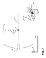
- FIG 2 shows the lithographic apparatus 1 in more detail, including a radiation system 42, an illumination optics unit 44, and a projection system PL.
- the radiation system 42 includes the radiation source SO.
- Embodiments of the source SO are depicted in Figures 3-6 .
- the source SO is configured to produce extreme ultraviolet radiation emitted by a plasma P.
- a plasma P may be produced by irradiating a droplet D (see Figure 3 ) of a fuel material, such as tin (Sn) droplets which may be supplied by a fuel material supply SP ( Figure 3 ) constructed and arranged for this purpose.
- the radiation source SO may include a laser L, for instance a CO 2 laser, to irradiate the droplet D.
- a hot plasma is created, for example by causing a partially ionized plasma to collapse onto an optical axis O.
- the hot plasma created emits radiation in the EUV range of the electromagnetic spectrum.
- This source may be referred to as a laser-produced plasma (LPP) source.
- the radiation source SO may comprise a source chamber 47.
- the source SO may also comprise a contamination trap 49 and a collector 50, however, the contamination trap 49 and collector 50 do not have to be part of the source SO.
- the EUV radiation emitted by plasma P is reflected by the collector 50 to be focused to a focal point 52 via the gas barrier structure or contamination trap 49 which may be positioned in source chamber 47.
- the gas barrier structure/contamination trap 49 includes a channel structure such as described in detail in U.S. Patent Nos. 6,614,505 and 6,359,969 .
- the chamber comprises hydrogen.
- the gas in the chamber substantially only comprises hydrogen.
- the embodiment illustrated in Figure 2 includes a spectral filter 51.
- radiation reflected by the collector 50 may be reflected off a grating spectral filter 51 to be focused in the focal point 52.
- a transmissive spectral filter may be applied, configured to transmit the EUV radiation.
- the radiation beam 56 thus formed is reflected in illumination optics unit 44 via normal incidence reflectors 53, 54 onto a patterning device (e.g. reticle or mask) positioned on patterning device support (e.g. reticle or mask table) MT.
- a patterned beam 57 is formed which is imaged in projection system PL via reflective elements 58, 59 onto substrate table WT. More elements than shown may generally be present in illumination optics unit 44 and projection system PL.
- the radiation collector 50 may be a collector as described in European Patent Application Publication No. EP1394612 , which is incorporated herein by reference.
- the radiation collector is one or more collectors selected from the group of: a collector configured to focus collected radiation into the radiation beam emission aperture, a collector having a first focal point that coincides with the source and a second focal point that coincides with the radiation beam emission aperture, a normal incidence collector, a collector having a single substantially ellipsoid radiation collecting surface section, and/or a Schwarzschild collector having two radiation collecting surfaces.
- the radiation source SO may be a discharge-produced plasma (DPP) source.
- DPP discharge-produced plasma
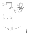
- FIG 3 depicts a more detailed view of the radiation source SO of Figure 2 .
- the supply SP provides droplets D, while the laser irradiates these droplets thereby forming a plasma P thus creating EUV radiation.
- the plasma P may produce debris in the form of atoms, ions or micro-particles MP.
- Micro-particles although generally several orders of magnitude smaller than droplet D, are liquid material themselves and can thus be regarded as further droplets.
- the micro-particles can have a diameter in the range of about 0.01- 5 ⁇ m, for example 0.01-0.1 ⁇ m).
- the radiation source SO of Figures 2 and 3 is further provided with an evaporating element 60, for example a plate 60, having an evaporation surface 62.
- the evaporating element can have various shapes and dimensions, and may be located in various positions and orientations. Some advantageous examples of the evaporating element 60 will be described below.
- the surface 62 may be provided by several materials, for example molybdenum (Mo), tungsten (W), and rhenium (Re), or other materials.
- the evaporation surface 62 may be a substantially smooth surface, however, the surface is preferably a rough surface.
- the surface 62 can be provided with a surface enlarging structure or configuration, for example by having surface enlargement fins or a roughening structure.
- the surface 62 is provided with a particle capturing structure, for example by providing a porous surface 62, or a surface having a particle capturing mesh.
- the surface 62 can be provided with a divider structure, for example having sharp edges, to split relative large incoming particles into smaller ones, before being evaporated. In this way, a very efficient particle evaporation is expected to be achieved.
- the evaporation surface 62 is configured to mitigate the debris particles during operation by evaporating the particles upon impact.
- a heating system 64 is provided, for example comprising a heating device, for example a resistor 68 or another suitable heating device, located inside the plate 60.
- the heating system 64 is provided with a temperature sensor 70 arranged to measure the temperature of the evaporation surface and a pressure sensor 72 constructed and arranged to measure a pressure in a direct vicinity of the surface.
- a power supply 66 can be provided, to power the heating device 68.
- an outlet 74 is provided which is in a fluid connection with a pump 76.
- heat can be supplied to the evaporating surface utilizing a heating device 68 that is located near the surface (for example by being integrated in the constructional element 60 that provides the surface 62).
- a heating device 68 that is located near the surface (for example by being integrated in the constructional element 60 that provides the surface 62).
- an external heating device can be applied, for example a heat radiating device configured to transmit heat radiation to the evaporating surface, or to the element 60.
- the surface 60 (or another part of the element 60) can be configured to substantially absorb such radiation, in order to heat up the evaporation surface 62.
- the temperature sensor can be located near the evaporating surface 62 (for example by being integrated in the constructional element 60).
- one or more external sensors can be applied, for example a pyrometer, to detect the temperature at or near the evaporating surface 62.
- the heating system is constructed and arranged to maintain the evaporation surface 62 at a surface temperature, such that a pressure in a direct vicinity of the surface 62 is below a vapor pressure for the surface temperature, the vapor pressure being the vapor pressure of the particle material MP which, in use, is emitted by the plasma P as a by-product (towards the surface 62).
- the heating system 64 heats the element 60 such that the temperature of the evaporation surface 62 is at a temperature, wherein the pressure measured by the pressure sensor is below a vapor pressure for the evaporation surface temperature.
- the evaporation surface 62 is maintained at a high temperature to evaporate the inbound particles MP.
- a micro-particle incident on the evaporation surface may be evaporated substantially instantaneously.
- the resulting gas, resulting from the evaporation of the particle MP is desirably diverted away from the collector chamber 47, for example by pump 76 via outlet 74.
- a typical Sn droplet diameter may be 50 ⁇ m. Because the specific heat capacity and the evaporation enthalpy are known for liquid Sn, it can be calculated that about 1.5 mJ per droplet is desired to evaporate Sn. At a rate of 50,000 droplets per second, this results in a power of 75 W.
- Particles created in the plasma P will be emitted in all directions, for example by scattering in the full 4 Pi. However, more particles are typically emitted in a certain direction than in others. For example, most particles have a preferred scattering direction. This direction is determined by the superposition of forces caused by gas flow, gravitation, and a laser pointing vector (for example the laser direction and intensity). Adding this to the initial droplet momentum results in a vector indicating the direction from the plasma in which more of the material is emitted than in other directions. Desirably, the evaporation surface 62 is located in this direction when viewed from the plasma P.
- Table 1 discloses several vapor pressures for certain surface temperatures, indicating that the tin (Sn) boiling temperature reduces with lower vapour pressure.
- the table indicates variation of the temperature of the evaporation surface 62 from about 1475 K to about 2900 K, and respective Sn vapour pressures varying between about 1 Pa and 100 kPa, i.e. several orders of magnitude.
- Suitable evaporation surface materials that can be heated to temperatures within this range are molybdenum (Mo), tungsten (W), and rhenium (Re).
- Mo molybdenum
- W tungsten
- Re rhenium
- FIG. 4 A modification of the radiation source is depicted in Figure 4 .
- a cone-shaped outlet 74 is provided.
- one or more cooling rings 78 are provided inside the cone-shaped outlet 74, also referred to as an extraction cone.
- an additional or other cooling device may be provided instead of a cooling ring 78.
- a cooling spiral may be provided on the inside of the cone-shaped outlet 74.
- Operation of the Figure 4 embodiment includes a cooling of the gas flow flowing through the outlet 74, such, that evaporated debris (present in the gas flow) can condense. Resulting liquid debris material can be caught by the outlet 74 itself (for example by the cooling rings 78), for example to recycle the material.
- the rings 78 can prevent liquefied debris material to flow back towards the source vessel.
- a device to recycle the evaporated debris particles MP can also be configured in a different manner.
- a liquefying system to liquefy (and preferably collect) the evaporated particle material can be located upstream with respect to the outlet 74, for example between the pump 76 and the outlet 74, or in a different location.
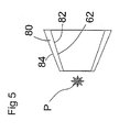
- FIG. 5 Another modification of the radiation source is disclosed referring to Figure 5 , and desirably comprises double sided walls.
- the radiation source disclosed referring to Figure 5 is quite similar.
- the evaporation surface 62 is provided on a conically-shaped body 80 having an inner surface 82 and an outer surface 84.
- the evaporation surface 62 of the conically-shaped body is located on the inner surface 82 of the conically-shaped body 80.
- the inner surface 82 may be provided with a low-emissivity material and/or the outer surface 84 may be provided with a high- emissivity material.
- a well-polished metal such as polished molybdenum (Mo) or tungsten (W), may be used as the low-emitting material.
- a ceramic material may be used as the high-emitting material.
- the outside wall 84 is preferably cooled. In this way the side wall heat transfer can be significantly limited, thus decreasing the power needed to put in (to heat the evaporation surface).
- the evaporation surface 62 may at least partially be a rough surface.
- the surface 62 can be made micro rough, to increase sticking and residence time of incoming debris particles.
- the surface 62 may have a root mean square (RMS) roughness of between about 10 nm and about 1 mm, desirably between about 50 nm and about 10 ⁇ m.
- RMS root mean square
- the surface can be both macro and micro rough. The rough surface can increase sticking and residence time significantly.
- the evaporation surface 62 may be a surface of the gas barrier structure/contamination trap 49.
- the conically-shaped body 80 with the evaporation surface 62 may be part of the gas barrier structure/contamination trap 49.
- hydrogen radicals may be generated and provided at a location proximate a surface (e.g., a surface of the plate 60, a surface of a collector mirror) such that the hydrogen radicals react with debris deposited on the surface.
- a surface e.g., a surface of the plate 60, a surface of a collector mirror
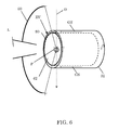
- Figure 6 depicts another example of the radiation source. Compared to the radiation source of Figures 3 and 4 , the radiation source disclosed referring to Figure 6 is, again, quite similar.
- the embodiment according to Figure 6 provides reduced reflection of particles, especially on the edges EV of the vaporizer, located near a plasma creation region (see drawing). Particularly, the Figure 6 embodiment can reduce chances that particles scattered on these locations are stopped by a regular buffer gas flow, preventing such particles to reach the collector.
- the source may be provided with a gas injector arranged to inject a gas flow into the source chamber at an edge EV of the evaporation surface 62.
- the gas injector can be arranged in various ways.
- the injector is configured to feed gas along an outer surface of the debris particle vaporizer element 80, towards and along a proximal (in this case circular) edge of that element 80.
- the gas injector can be configured to inject a ring-shaped gas curtain, into the source chamber.
- a pump may be provided (not shown in Figure 6 ) to remove evaporated particles from the interior of the vaporizer 80; a respective pumping flow (towards the pump, and away from the collector 50) is indicated by arrows PD in Figure 6 .
- the pumping flow PD draws the gas curtain, injected by the injector, inwardly, towards the plasma P and into the vaporizer, to be exhausted via the vaporizer towards the pump.
- the gas curtain can substantially enclose the proximal edge EV of the vaporizer element 80, to shield the edge from the opposite collector's surface.
- debris captured and/or decelerated by the gas curtain can be pumped away as well (via the vaporizer interior).
- the gas injector can include a secondary element 92, extending around a debris particle vaporizer element (for example cone) 80. With this secondary element 92, backfill gas can be supplied to the edge region where the particles have a relatively high scattering chance.
- a respective gas flow of the backfill gas is indicated by arrows GS in Figure 6 .
- the gas is desirably an inert gas with a high mass (comparable to tin), e.g. Argon, Krypton, Xenon.
- the injector is configured to supply the case to all parts of the edge EV, for example in the form of a gas curtain.
- lithographic apparatus in the manufacture of ICs
- the lithographic apparatus described herein may have other applications, such as the manufacture of integrated optical systems, guidance and detection patterns for magnetic domain memories, flat-panel displays, liquid-crystal displays (LCDs), thin-film magnetic heads, etc.
- any use of the terms “wafer” or “die” herein may be considered as synonymous with the more general terms “substrate” or “target portion”, respectively.
- the substrate referred to herein may be processed, before or after exposure, in for example a track (a tool that typically applies a layer of resist to a substrate and develops the exposed resist), a metrology tool and/or an inspection tool. Where applicable, the disclosure herein may be applied to such and other substrate processing tools. Further, the substrate may be processed more than once, for example in order to create a multi-layer IC, so that the term substrate used herein may also refer to a substrate that already contains multiple processed layers.
Claims (9)
- Eine Strahlungsquelle (SO), die konfiguriert ist, um extrem ultraviolette Strahlung zu produzieren, wobei die Strahlungsquelle (SO) Folgendes beinhaltet:eine Kammer (47), in der bei Gebrauch ein Plasma (P) erzeugt wird und das Plasma (P) Debris in Form von Teilchen als ein Nebenprodukt produziert;einen Kollektorspiegel (50), der konfiguriert ist, um von dem Plasma emittierte Strahlung auf einen Brennpunkt (52) zu fokussieren; undein Heizsystem (64) und eine Verdampfungsoberfläche (62), wobei das Heizsystem (64) konstruiert und eingerichtet ist, um die Verdampfungsoberfläche (62) bei einer Oberflächentemperatur zu halten, so dass ein Druck in einer direkten Nachbarschaft der Verdampfungsoberfläche (62) unter einem Dampfdruck für die Oberflächentemperatur liegt, wobei der Dampfdruck der Dampfdruck von Zinn ist, das von dem Plasma (P) bei Gebrauch als ein Nebenprodukt emittiert wird, wobei das Heizsystem (64) Folgendes beinhaltet:einen Temperatursensor (70), der konfiguriert ist, um die Temperatur auf der Verdampfungsoberfläche (62) zu messen; undeinen Drucksensor (72), der konfiguriert ist, um den Druck in einer direkten Nachbarschaft der Verdampfungsoberfläche (62) zu messen, und die Verdampfungsoberfläche (62) konfiguriert ist, um die Debristeilchen während des Betriebs durch Verdampfen der Teilchen bei Aufprall abzuschwächen, wobei das Heizsystem (64) konfiguriert ist, um die Verdampfungsoberfläche (62) zu erhitzen, wenn der von dem Drucksensor (72) gemessene Druck über dem Dampfdruck bei der von dem Temperatursensor (70) gemessenen Temperatur liegt.
- Strahlungsquelle (SO) gemäß Anspruch 1, wobei der Kollektorspiegel (50) das erste optische Element in einem optischen Weg der von dem Plasma emittierten Strahlung ist.
- Strahlungsquelle (SO) gemäß einem der vorhergehenden Ansprüche, wobei die Oberfläche (62) ein oder mehrere Materialen beinhaltet, die aus der aus Mo, W und Re bestehenden Gruppe ausgewählt sind.
- Strahlungsquelle (SO) gemäß einem der vorhergehenden Ansprüche, die ferner einen mindestens teilweise konisch geformten Körper (80) beinhaltet.
- Strahlungsquelle (SO) gemäß Anspruch 4, wobei der mindestens teilweise konisch geformte Körper (80) die Verdampfungsoberfläche (62) beinhaltet.
- Strahlungsquelle (SO) gemäß Anspruch 5, wobei sich die Verdampfoberfläche (62) auf einer inneren Oberfläche des konisch geformten Körpers (80) befindet.
- Strahlungsquelle (SO) gemäß Anspruch 4, wobei eine äußere Oberfläche des konisch geformten Körpers (80) gekühlt wird.
- Ein lithographisches Gerät, das eine Strahlungsquelle (SO) gemäß einem der vorhergehenden Ansprüche beinhaltet.
- Ein Verfahren zum Entfernen von Debris in Form von Teilchen als einem Nebenproduktmaterial in oder aus einer extrem ultravioletten Plasma-Strahlungsquelle (SO) eines lithographischen Geräts, wobei das Verfahren Folgendes beinhaltet:Verwenden eines Heizsystems (64) und einer Verdampfungsoberfläche (62), wobei das Heizsystem (64) konstruiert und eingerichtet ist, um die Verdampfungsoberfläche (62) bei einer Oberflächentemperatur zu halten, wobei ein Druck in einer direkten Nachbarschaft der Oberfläche (62) unter einem Dampfdruck für die Oberflächentemperatur liegt, wobei der Dampfdruck der Dampfdruck des Nebenproduktmaterials Zinn ist und das Verfahren das Messen der Temperatur auf der Verdampfungsoberfläche (62) mit einem Temperatursensor (70) unddas Messen des Drucks in einer direkten Nachbarschaft der Verdampfungsoberfläche (62) mit einem Drucksensor (72) beinhaltet, um mit der Verdampfungsoberfläche (62) die Debristeilchen während des Betriebs durch Verdampfen der Teilchen bei Aufprall abzuschwächen, und das Heizsystem (64) konfiguriert ist, um die Verdampfungsoberfläche (62) zu erhitzen, wenn der von dem Drucksensor (72) gemessene Druck über dem Dampfdruck bei der von dem Temperatursensor (70) gemessenen Temperatur liegt.
Applications Claiming Priority (3)
| Application Number | Priority Date | Filing Date | Title |
|---|---|---|---|
| US13642808P | 2008-09-04 | 2008-09-04 | |
| US13645108P | 2008-09-05 | 2008-09-05 | |
| US19381408P | 2008-12-24 | 2008-12-24 |
Publications (3)
| Publication Number | Publication Date |
|---|---|
| EP2161725A2 EP2161725A2 (de) | 2010-03-10 |
| EP2161725A3 EP2161725A3 (de) | 2012-06-13 |
| EP2161725B1 true EP2161725B1 (de) | 2015-07-08 |
Family
ID=41396260
Family Applications (1)
| Application Number | Title | Priority Date | Filing Date |
|---|---|---|---|
| EP09167126.3A Active EP2161725B1 (de) | 2008-09-04 | 2009-08-27 | Strahlungsquelle und entsprechendes Verfahren |
Country Status (3)
| Country | Link |
|---|---|
| US (2) | US8373846B2 (de) |
| EP (1) | EP2161725B1 (de) |
| JP (1) | JP5162546B2 (de) |
Cited By (1)
| Publication number | Priority date | Publication date | Assignee | Title |
|---|---|---|---|---|
| WO2023041306A1 (en) * | 2021-09-15 | 2023-03-23 | Asml Netherlands B.V. | Apparatus and method for actively heating a substrate in an euv light source |
Families Citing this family (10)
| Publication number | Priority date | Publication date | Assignee | Title |
|---|---|---|---|---|
| EP2161725B1 (de) * | 2008-09-04 | 2015-07-08 | ASML Netherlands B.V. | Strahlungsquelle und entsprechendes Verfahren |
| EP2321704B1 (de) * | 2008-09-11 | 2018-06-13 | ASML Netherlands BV | Strahlungsquelle und lithografischer apparat |
| JP5559562B2 (ja) | 2009-02-12 | 2014-07-23 | ギガフォトン株式会社 | 極端紫外光光源装置 |
| DE102010041298A1 (de) | 2010-09-24 | 2012-03-29 | Carl Zeiss Smt Gmbh | EUV-Mikrolithographie-Projektionsbelichtungsanlage mit einer Heizlichtquelle |
| WO2013127587A2 (en) * | 2012-02-27 | 2013-09-06 | Asml Netherlands B.V. | Source collector apparatus, lithographic apparatus and device manufacturing method |
| JP2015528994A (ja) * | 2012-08-01 | 2015-10-01 | エーエスエムエル ネザーランズ ビー.ブイ. | 放射を発生させるための方法及び装置 |
| WO2014121873A1 (en) * | 2013-02-08 | 2014-08-14 | Asml Netherlands B.V. | Radiation source for an euv optical lithographic apparatus, and lithographic apparatus comprising such a power source |
| EP3416180A1 (de) * | 2017-06-18 | 2018-12-19 | Excillum AB | Röntgenstrahlenquelle mit temperatursteuergerät |
| US11272606B2 (en) | 2017-06-27 | 2022-03-08 | Taiwan Semiconductor Manufacturing Co., Ltd. | EUV light source and apparatus for lithography |
| NL2021345A (en) * | 2018-04-12 | 2018-08-22 | Asml Netherlands Bv | Lithographic apparatus |
Citations (4)
| Publication number | Priority date | Publication date | Assignee | Title |
|---|---|---|---|---|
| JPH08159991A (ja) * | 1994-12-08 | 1996-06-21 | Nikon Corp | X線装置 |
| US20040135517A1 (en) * | 2002-10-30 | 2004-07-15 | Xtreme Technologies Gmbh | Radiation source for generating extreme ultraviolet radiation |
| US20050111080A1 (en) * | 2003-10-20 | 2005-05-26 | Asml Netherlands B.V. | Mirror for use in a lithographic apparatus, lithographic apparatus, device manufacturing method, and device manufactured thereby |
| US20060097203A1 (en) * | 2004-11-01 | 2006-05-11 | Cymer, Inc. | Systems and methods for cleaning a chamber window of an EUV light source |
Family Cites Families (17)
| Publication number | Priority date | Publication date | Assignee | Title |
|---|---|---|---|---|
| US6815700B2 (en) * | 1997-05-12 | 2004-11-09 | Cymer, Inc. | Plasma focus light source with improved pulse power system |
| NL1008352C2 (nl) | 1998-02-19 | 1999-08-20 | Stichting Tech Wetenschapp | Inrichting, geschikt voor extreem ultraviolet lithografie, omvattende een stralingsbron en een verwerkingsorgaan voor het verwerken van de van de stralingsbron afkomstige straling, alsmede een filter voor het onderdrukken van ongewenste atomaire en microscopische deeltjes welke door een stralingsbron zijn uitgezonden. |
| US6614505B2 (en) | 2001-01-10 | 2003-09-02 | Asml Netherlands B.V. | Lithographic projection apparatus, device manufacturing method, and device manufactured thereby |
| DE10219173A1 (de) * | 2002-04-30 | 2003-11-20 | Philips Intellectual Property | Verfahren zur Erzeugung von Extrem-Ultraviolett-Strahlung |
| EP1394612B1 (de) | 2002-08-27 | 2008-10-08 | ASML Netherlands B.V. | Lithographischer Projektionsapparat und Reflektoranordnung für die Verwendung in diesem Apparat |
| EP1629268B1 (de) * | 2003-05-22 | 2013-05-15 | Philips Intellectual Property & Standards GmbH | Verfahren und vorrichtung zum reinigen mindestens einer optischen komponente |
| US7098994B2 (en) * | 2004-01-16 | 2006-08-29 | Asml Netherlands B.V. | Lithographic apparatus, device manufacturing method, and device manufactured thereby |
| US8075732B2 (en) * | 2004-11-01 | 2011-12-13 | Cymer, Inc. | EUV collector debris management |
| DE102005020521B4 (de) * | 2005-04-29 | 2013-05-02 | Xtreme Technologies Gmbh | Verfahren und Anordnung zur Unterdrückung von Debris bei der Erzeugung kurzwelliger Strahlung auf Basis eines Plasmas |
| JP2008544448A (ja) * | 2005-06-14 | 2008-12-04 | コーニンクレッカ フィリップス エレクトロニクス エヌ ヴィ | Euv放射線及び/又は軟x線を発生させる放射線源を短絡から保護する方法 |
| US7561247B2 (en) * | 2005-08-22 | 2009-07-14 | Asml Netherlands B.V. | Method for the removal of deposition on an optical element, method for the protection of an optical element, device manufacturing method, apparatus including an optical element, and lithographic apparatus |
| JP2007134166A (ja) * | 2005-11-10 | 2007-05-31 | Ushio Inc | 極端紫外光光源装置 |
| US7696493B2 (en) * | 2006-12-13 | 2010-04-13 | Asml Netherlands B.V. | Radiation system and lithographic apparatus |
| JP5086664B2 (ja) * | 2007-03-02 | 2012-11-28 | ギガフォトン株式会社 | 極端紫外光源装置 |
| JP5277496B2 (ja) * | 2007-04-27 | 2013-08-28 | ギガフォトン株式会社 | 極端紫外光源装置および極端紫外光源装置の光学素子汚染防止装置 |
| US8054446B2 (en) * | 2008-08-21 | 2011-11-08 | Carl Zeiss Smt Gmbh | EUV lithography apparatus and method for determining the contamination status of an EUV-reflective optical surface |
| EP2161725B1 (de) | 2008-09-04 | 2015-07-08 | ASML Netherlands B.V. | Strahlungsquelle und entsprechendes Verfahren |
-
2009
- 2009-08-27 EP EP09167126.3A patent/EP2161725B1/de active Active
- 2009-08-28 JP JP2009197591A patent/JP5162546B2/ja active Active
- 2009-09-03 US US12/553,368 patent/US8373846B2/en active Active
-
2012
- 2012-11-27 US US13/686,633 patent/US8946661B2/en active Active
Patent Citations (4)
| Publication number | Priority date | Publication date | Assignee | Title |
|---|---|---|---|---|
| JPH08159991A (ja) * | 1994-12-08 | 1996-06-21 | Nikon Corp | X線装置 |
| US20040135517A1 (en) * | 2002-10-30 | 2004-07-15 | Xtreme Technologies Gmbh | Radiation source for generating extreme ultraviolet radiation |
| US20050111080A1 (en) * | 2003-10-20 | 2005-05-26 | Asml Netherlands B.V. | Mirror for use in a lithographic apparatus, lithographic apparatus, device manufacturing method, and device manufactured thereby |
| US20060097203A1 (en) * | 2004-11-01 | 2006-05-11 | Cymer, Inc. | Systems and methods for cleaning a chamber window of an EUV light source |
Cited By (1)
| Publication number | Priority date | Publication date | Assignee | Title |
|---|---|---|---|---|
| WO2023041306A1 (en) * | 2021-09-15 | 2023-03-23 | Asml Netherlands B.V. | Apparatus and method for actively heating a substrate in an euv light source |
Also Published As
| Publication number | Publication date |
|---|---|
| US8946661B2 (en) | 2015-02-03 |
| EP2161725A3 (de) | 2012-06-13 |
| US8373846B2 (en) | 2013-02-12 |
| US20130327955A1 (en) | 2013-12-12 |
| JP2010062560A (ja) | 2010-03-18 |
| JP5162546B2 (ja) | 2013-03-13 |
| US20100053576A1 (en) | 2010-03-04 |
| EP2161725A2 (de) | 2010-03-10 |
Similar Documents
| Publication | Publication Date | Title |
|---|---|---|
| EP2161725B1 (de) | Strahlungsquelle und entsprechendes Verfahren | |
| US7639418B2 (en) | Multi-layer spectral purity filter, lithographic apparatus including such a spectral purity filter, device manufacturing method, and device manufactured thereby | |
| US9207548B2 (en) | Radiation source with a debris mitigation system, lithographic apparatus with a debris mitigation system, method for preventing debris from depositing on collector mirror, and device manufacturing method | |
| EP2561407B1 (de) | Kollektorspiegelanordnung und verfahren zur produktion von euv strahlung | |
| JP2010062560A5 (de) | ||
| US9563137B2 (en) | Lithographic apparatus and device manufacturing method | |
| EP2154574A2 (de) | Strahlungsquellen und Verfahren zur Strahlungserzeugung | |
| US10678140B2 (en) | Suppression filter, radiation collector and radiation source for a lithographic apparatus; method of determining a separation distance between at least two reflective surface levels of a suppression filter | |
| EP2310912B1 (de) | Strahlungsquelle, lithographische vorrichtung und vorrichtungsherstellungsverfahren | |
| US20120006258A1 (en) | Hydrogen radical generator | |
| US9846365B2 (en) | Component for a radiation source, associated radiation source and lithographic apparatus | |
| EP2480935A1 (de) | Filter für spektrale reinheit, lithografisches gerät und geräteherstellungsverfahren | |
| US9778574B2 (en) | Apparatus, a device and a device manufacturing method | |
| NL2010236A (en) | Lithographic apparatus and method. | |
| NL2011773A (en) | Component for a radiation source, associated radiation source and lithographic apparatus. | |
| NL2005763A (en) | Lithographic apparatus. |
Legal Events
| Date | Code | Title | Description |
|---|---|---|---|
| PUAI | Public reference made under article 153(3) epc to a published international application that has entered the european phase |
Free format text: ORIGINAL CODE: 0009012 |
|
| AK | Designated contracting states |
Kind code of ref document: A2 Designated state(s): AT BE BG CH CY CZ DE DK EE ES FI FR GB GR HR HU IE IS IT LI LT LU LV MC MK MT NL NO PL PT RO SE SI SK SM TR |
|
| AX | Request for extension of the european patent |
Extension state: AL BA RS |
|
| RIC1 | Information provided on ipc code assigned before grant |
Ipc: G21K 1/06 20060101AFI20120302BHEP Ipc: H05G 2/00 20060101ALI20120302BHEP Ipc: G03F 7/20 20060101ALI20120302BHEP |
|
| PUAL | Search report despatched |
Free format text: ORIGINAL CODE: 0009013 |
|
| AK | Designated contracting states |
Kind code of ref document: A3 Designated state(s): AT BE BG CH CY CZ DE DK EE ES FI FR GB GR HR HU IE IS IT LI LT LU LV MC MK MT NL NO PL PT RO SE SI SK SM TR |
|
| AX | Request for extension of the european patent |
Extension state: AL BA RS |
|
| RIC1 | Information provided on ipc code assigned before grant |
Ipc: G03F 7/20 20060101ALI20120508BHEP Ipc: H05G 2/00 20060101ALI20120508BHEP Ipc: G21K 1/06 20060101AFI20120508BHEP |
|
| 17P | Request for examination filed |
Effective date: 20121210 |
|
| 17Q | First examination report despatched |
Effective date: 20130913 |
|
| GRAP | Despatch of communication of intention to grant a patent |
Free format text: ORIGINAL CODE: EPIDOSNIGR1 |
|
| INTG | Intention to grant announced |
Effective date: 20150320 |
|
| GRAS | Grant fee paid |
Free format text: ORIGINAL CODE: EPIDOSNIGR3 |
|
| GRAA | (expected) grant |
Free format text: ORIGINAL CODE: 0009210 |
|
| AK | Designated contracting states |
Kind code of ref document: B1 Designated state(s): AT BE BG CH CY CZ DE DK EE ES FI FR GB GR HR HU IE IS IT LI LT LU LV MC MK MT NL NO PL PT RO SE SI SK SM TR |
|
| REG | Reference to a national code |
Ref country code: GB Ref legal event code: FG4D |
|
| REG | Reference to a national code |
Ref country code: AT Ref legal event code: REF Ref document number: 735938 Country of ref document: AT Kind code of ref document: T Effective date: 20150715 Ref country code: CH Ref legal event code: EP |
|
| REG | Reference to a national code |
Ref country code: IE Ref legal event code: FG4D |
|
| REG | Reference to a national code |
Ref country code: DE Ref legal event code: R096 Ref document number: 602009032047 Country of ref document: DE Ref country code: FR Ref legal event code: PLFP Year of fee payment: 7 |
|
| REG | Reference to a national code |
Ref country code: AT Ref legal event code: MK05 Ref document number: 735938 Country of ref document: AT Kind code of ref document: T Effective date: 20150708 |
|
| REG | Reference to a national code |
Ref country code: NL Ref legal event code: MP Effective date: 20150708 |
|
| REG | Reference to a national code |
Ref country code: LT Ref legal event code: MG4D |
|
| PG25 | Lapsed in a contracting state [announced via postgrant information from national office to epo] |
Ref country code: FI Free format text: LAPSE BECAUSE OF FAILURE TO SUBMIT A TRANSLATION OF THE DESCRIPTION OR TO PAY THE FEE WITHIN THE PRESCRIBED TIME-LIMIT Effective date: 20150708 Ref country code: LT Free format text: LAPSE BECAUSE OF FAILURE TO SUBMIT A TRANSLATION OF THE DESCRIPTION OR TO PAY THE FEE WITHIN THE PRESCRIBED TIME-LIMIT Effective date: 20150708 Ref country code: GR Free format text: LAPSE BECAUSE OF FAILURE TO SUBMIT A TRANSLATION OF THE DESCRIPTION OR TO PAY THE FEE WITHIN THE PRESCRIBED TIME-LIMIT Effective date: 20151009 Ref country code: NO Free format text: LAPSE BECAUSE OF FAILURE TO SUBMIT A TRANSLATION OF THE DESCRIPTION OR TO PAY THE FEE WITHIN THE PRESCRIBED TIME-LIMIT Effective date: 20151008 Ref country code: LV Free format text: LAPSE BECAUSE OF FAILURE TO SUBMIT A TRANSLATION OF THE DESCRIPTION OR TO PAY THE FEE WITHIN THE PRESCRIBED TIME-LIMIT Effective date: 20150708 |
|
| PG25 | Lapsed in a contracting state [announced via postgrant information from national office to epo] |
Ref country code: HR Free format text: LAPSE BECAUSE OF FAILURE TO SUBMIT A TRANSLATION OF THE DESCRIPTION OR TO PAY THE FEE WITHIN THE PRESCRIBED TIME-LIMIT Effective date: 20150708 Ref country code: PL Free format text: LAPSE BECAUSE OF FAILURE TO SUBMIT A TRANSLATION OF THE DESCRIPTION OR TO PAY THE FEE WITHIN THE PRESCRIBED TIME-LIMIT Effective date: 20150708 Ref country code: PT Free format text: LAPSE BECAUSE OF FAILURE TO SUBMIT A TRANSLATION OF THE DESCRIPTION OR TO PAY THE FEE WITHIN THE PRESCRIBED TIME-LIMIT Effective date: 20151109 Ref country code: SE Free format text: LAPSE BECAUSE OF FAILURE TO SUBMIT A TRANSLATION OF THE DESCRIPTION OR TO PAY THE FEE WITHIN THE PRESCRIBED TIME-LIMIT Effective date: 20150708 Ref country code: IS Free format text: LAPSE BECAUSE OF FAILURE TO SUBMIT A TRANSLATION OF THE DESCRIPTION OR TO PAY THE FEE WITHIN THE PRESCRIBED TIME-LIMIT Effective date: 20151108 Ref country code: ES Free format text: LAPSE BECAUSE OF FAILURE TO SUBMIT A TRANSLATION OF THE DESCRIPTION OR TO PAY THE FEE WITHIN THE PRESCRIBED TIME-LIMIT Effective date: 20150708 Ref country code: AT Free format text: LAPSE BECAUSE OF FAILURE TO SUBMIT A TRANSLATION OF THE DESCRIPTION OR TO PAY THE FEE WITHIN THE PRESCRIBED TIME-LIMIT Effective date: 20150708 |
|
| REG | Reference to a national code |
Ref country code: CH Ref legal event code: PL |
|
| REG | Reference to a national code |
Ref country code: DE Ref legal event code: R097 Ref document number: 602009032047 Country of ref document: DE |
|
| PG25 | Lapsed in a contracting state [announced via postgrant information from national office to epo] |
Ref country code: LI Free format text: LAPSE BECAUSE OF NON-PAYMENT OF DUE FEES Effective date: 20150831 Ref country code: IT Free format text: LAPSE BECAUSE OF FAILURE TO SUBMIT A TRANSLATION OF THE DESCRIPTION OR TO PAY THE FEE WITHIN THE PRESCRIBED TIME-LIMIT Effective date: 20150708 Ref country code: DK Free format text: LAPSE BECAUSE OF FAILURE TO SUBMIT A TRANSLATION OF THE DESCRIPTION OR TO PAY THE FEE WITHIN THE PRESCRIBED TIME-LIMIT Effective date: 20150708 Ref country code: MC Free format text: LAPSE BECAUSE OF FAILURE TO SUBMIT A TRANSLATION OF THE DESCRIPTION OR TO PAY THE FEE WITHIN THE PRESCRIBED TIME-LIMIT Effective date: 20150708 Ref country code: EE Free format text: LAPSE BECAUSE OF FAILURE TO SUBMIT A TRANSLATION OF THE DESCRIPTION OR TO PAY THE FEE WITHIN THE PRESCRIBED TIME-LIMIT Effective date: 20150708 Ref country code: CH Free format text: LAPSE BECAUSE OF NON-PAYMENT OF DUE FEES Effective date: 20150831 Ref country code: CZ Free format text: LAPSE BECAUSE OF FAILURE TO SUBMIT A TRANSLATION OF THE DESCRIPTION OR TO PAY THE FEE WITHIN THE PRESCRIBED TIME-LIMIT Effective date: 20150708 Ref country code: SK Free format text: LAPSE BECAUSE OF FAILURE TO SUBMIT A TRANSLATION OF THE DESCRIPTION OR TO PAY THE FEE WITHIN THE PRESCRIBED TIME-LIMIT Effective date: 20150708 |
|
| PLBE | No opposition filed within time limit |
Free format text: ORIGINAL CODE: 0009261 |
|
| STAA | Information on the status of an ep patent application or granted ep patent |
Free format text: STATUS: NO OPPOSITION FILED WITHIN TIME LIMIT |
|
| PG25 | Lapsed in a contracting state [announced via postgrant information from national office to epo] |
Ref country code: RO Free format text: LAPSE BECAUSE OF FAILURE TO SUBMIT A TRANSLATION OF THE DESCRIPTION OR TO PAY THE FEE WITHIN THE PRESCRIBED TIME-LIMIT Effective date: 20150708 |
|
| REG | Reference to a national code |
Ref country code: IE Ref legal event code: MM4A |
|
| 26N | No opposition filed |
Effective date: 20160411 |
|
| GBPC | Gb: european patent ceased through non-payment of renewal fee |
Effective date: 20151008 |
|
| PG25 | Lapsed in a contracting state [announced via postgrant information from national office to epo] |
Ref country code: GB Free format text: LAPSE BECAUSE OF NON-PAYMENT OF DUE FEES Effective date: 20151008 Ref country code: IE Free format text: LAPSE BECAUSE OF NON-PAYMENT OF DUE FEES Effective date: 20150827 |
|
| REG | Reference to a national code |
Ref country code: FR Ref legal event code: PLFP Year of fee payment: 8 |
|
| PG25 | Lapsed in a contracting state [announced via postgrant information from national office to epo] |
Ref country code: SI Free format text: LAPSE BECAUSE OF FAILURE TO SUBMIT A TRANSLATION OF THE DESCRIPTION OR TO PAY THE FEE WITHIN THE PRESCRIBED TIME-LIMIT Effective date: 20150708 |
|
| PG25 | Lapsed in a contracting state [announced via postgrant information from national office to epo] |
Ref country code: MT Free format text: LAPSE BECAUSE OF FAILURE TO SUBMIT A TRANSLATION OF THE DESCRIPTION OR TO PAY THE FEE WITHIN THE PRESCRIBED TIME-LIMIT Effective date: 20150708 |
|
| PG25 | Lapsed in a contracting state [announced via postgrant information from national office to epo] |
Ref country code: HU Free format text: LAPSE BECAUSE OF FAILURE TO SUBMIT A TRANSLATION OF THE DESCRIPTION OR TO PAY THE FEE WITHIN THE PRESCRIBED TIME-LIMIT; INVALID AB INITIO Effective date: 20090827 Ref country code: BG Free format text: LAPSE BECAUSE OF FAILURE TO SUBMIT A TRANSLATION OF THE DESCRIPTION OR TO PAY THE FEE WITHIN THE PRESCRIBED TIME-LIMIT Effective date: 20150708 Ref country code: SM Free format text: LAPSE BECAUSE OF FAILURE TO SUBMIT A TRANSLATION OF THE DESCRIPTION OR TO PAY THE FEE WITHIN THE PRESCRIBED TIME-LIMIT Effective date: 20150708 |
|
| PG25 | Lapsed in a contracting state [announced via postgrant information from national office to epo] |
Ref country code: CY Free format text: LAPSE BECAUSE OF FAILURE TO SUBMIT A TRANSLATION OF THE DESCRIPTION OR TO PAY THE FEE WITHIN THE PRESCRIBED TIME-LIMIT Effective date: 20150708 Ref country code: NL Free format text: LAPSE BECAUSE OF FAILURE TO SUBMIT A TRANSLATION OF THE DESCRIPTION OR TO PAY THE FEE WITHIN THE PRESCRIBED TIME-LIMIT Effective date: 20150708 |
|
| PG25 | Lapsed in a contracting state [announced via postgrant information from national office to epo] |
Ref country code: BE Free format text: LAPSE BECAUSE OF NON-PAYMENT OF DUE FEES Effective date: 20150831 |
|
| REG | Reference to a national code |
Ref country code: FR Ref legal event code: PLFP Year of fee payment: 9 |
|
| PG25 | Lapsed in a contracting state [announced via postgrant information from national office to epo] |
Ref country code: TR Free format text: LAPSE BECAUSE OF FAILURE TO SUBMIT A TRANSLATION OF THE DESCRIPTION OR TO PAY THE FEE WITHIN THE PRESCRIBED TIME-LIMIT Effective date: 20150708 |
|
| PG25 | Lapsed in a contracting state [announced via postgrant information from national office to epo] |
Ref country code: LU Free format text: LAPSE BECAUSE OF NON-PAYMENT OF DUE FEES Effective date: 20150827 |
|
| PG25 | Lapsed in a contracting state [announced via postgrant information from national office to epo] |
Ref country code: MK Free format text: LAPSE BECAUSE OF FAILURE TO SUBMIT A TRANSLATION OF THE DESCRIPTION OR TO PAY THE FEE WITHIN THE PRESCRIBED TIME-LIMIT Effective date: 20150708 |
|
| REG | Reference to a national code |
Ref country code: FR Ref legal event code: PLFP Year of fee payment: 10 |
|
| P01 | Opt-out of the competence of the unified patent court (upc) registered |
Effective date: 20230403 |
|
| PGFP | Annual fee paid to national office [announced via postgrant information from national office to epo] |
Ref country code: FR Payment date: 20230824 Year of fee payment: 15 Ref country code: DE Payment date: 20230828 Year of fee payment: 15 |