EP2154714A2 - Temperature sensor with buffer layer - Google Patents
Temperature sensor with buffer layer Download PDFInfo
- Publication number
- EP2154714A2 EP2154714A2 EP09009135A EP09009135A EP2154714A2 EP 2154714 A2 EP2154714 A2 EP 2154714A2 EP 09009135 A EP09009135 A EP 09009135A EP 09009135 A EP09009135 A EP 09009135A EP 2154714 A2 EP2154714 A2 EP 2154714A2
- Authority
- EP
- European Patent Office
- Prior art keywords
- buffer layer
- temperature sensor
- chip
- housing
- sensitive structure
- Prior art date
- Legal status (The legal status is an assumption and is not a legal conclusion. Google has not performed a legal analysis and makes no representation as to the accuracy of the status listed.)
- Withdrawn
Links
Images


Classifications
-
- G—PHYSICS
- G01—MEASURING; TESTING
- G01N—INVESTIGATING OR ANALYSING MATERIALS BY DETERMINING THEIR CHEMICAL OR PHYSICAL PROPERTIES
- G01N27/00—Investigating or analysing materials by the use of electric, electrochemical, or magnetic means
- G01N27/02—Investigating or analysing materials by the use of electric, electrochemical, or magnetic means by investigating impedance
- G01N27/22—Investigating or analysing materials by the use of electric, electrochemical, or magnetic means by investigating impedance by investigating capacitance
- G01N27/223—Investigating or analysing materials by the use of electric, electrochemical, or magnetic means by investigating impedance by investigating capacitance for determining moisture content, e.g. humidity
-
- G—PHYSICS
- G01—MEASURING; TESTING
- G01D—MEASURING NOT SPECIALLY ADAPTED FOR A SPECIFIC VARIABLE; ARRANGEMENTS FOR MEASURING TWO OR MORE VARIABLES NOT COVERED IN A SINGLE OTHER SUBCLASS; TARIFF METERING APPARATUS; MEASURING OR TESTING NOT OTHERWISE PROVIDED FOR
- G01D3/00—Indicating or recording apparatus with provision for the special purposes referred to in the subgroups
- G01D3/028—Indicating or recording apparatus with provision for the special purposes referred to in the subgroups mitigating undesired influences, e.g. temperature, pressure
-
- G—PHYSICS
- G01—MEASURING; TESTING
- G01K—MEASURING TEMPERATURE; MEASURING QUANTITY OF HEAT; THERMALLY-SENSITIVE ELEMENTS NOT OTHERWISE PROVIDED FOR
- G01K7/00—Measuring temperature based on the use of electric or magnetic elements directly sensitive to heat ; Power supply therefor, e.g. using thermoelectric elements
- G01K7/01—Measuring temperature based on the use of electric or magnetic elements directly sensitive to heat ; Power supply therefor, e.g. using thermoelectric elements using semiconducting elements having PN junctions
-
- H—ELECTRICITY
- H01—ELECTRIC ELEMENTS
- H01L—SEMICONDUCTOR DEVICES NOT COVERED BY CLASS H10
- H01L21/00—Processes or apparatus adapted for the manufacture or treatment of semiconductor or solid state devices or of parts thereof
- H01L21/02—Manufacture or treatment of semiconductor devices or of parts thereof
- H01L21/04—Manufacture or treatment of semiconductor devices or of parts thereof the devices having at least one potential-jump barrier or surface barrier, e.g. PN junction, depletion layer or carrier concentration layer
- H01L21/50—Assembly of semiconductor devices using processes or apparatus not provided for in a single one of the subgroups H01L21/06 - H01L21/326, e.g. sealing of a cap to a base of a container
- H01L21/56—Encapsulations, e.g. encapsulation layers, coatings
- H01L21/565—Moulds
-
- H—ELECTRICITY
- H01—ELECTRIC ELEMENTS
- H01L—SEMICONDUCTOR DEVICES NOT COVERED BY CLASS H10
- H01L23/00—Details of semiconductor or other solid state devices
- H01L23/28—Encapsulations, e.g. encapsulating layers, coatings, e.g. for protection
- H01L23/31—Encapsulations, e.g. encapsulating layers, coatings, e.g. for protection characterised by the arrangement or shape
- H01L23/3157—Partial encapsulation or coating
- H01L23/3185—Partial encapsulation or coating the coating covering also the sidewalls of the semiconductor body
-
- H—ELECTRICITY
- H01—ELECTRIC ELEMENTS
- H01L—SEMICONDUCTOR DEVICES NOT COVERED BY CLASS H10
- H01L2224/00—Indexing scheme for arrangements for connecting or disconnecting semiconductor or solid-state bodies and methods related thereto as covered by H01L24/00
- H01L2224/01—Means for bonding being attached to, or being formed on, the surface to be connected, e.g. chip-to-package, die-attach, "first-level" interconnects; Manufacturing methods related thereto
- H01L2224/42—Wire connectors; Manufacturing methods related thereto
- H01L2224/47—Structure, shape, material or disposition of the wire connectors after the connecting process
- H01L2224/48—Structure, shape, material or disposition of the wire connectors after the connecting process of an individual wire connector
- H01L2224/4805—Shape
- H01L2224/4809—Loop shape
- H01L2224/48091—Arched
-
- H—ELECTRICITY
- H01—ELECTRIC ELEMENTS
- H01L—SEMICONDUCTOR DEVICES NOT COVERED BY CLASS H10
- H01L2924/00—Indexing scheme for arrangements or methods for connecting or disconnecting semiconductor or solid-state bodies as covered by H01L24/00
- H01L2924/10—Details of semiconductor or other solid state devices to be connected
- H01L2924/11—Device type
- H01L2924/12—Passive devices, e.g. 2 terminal devices
- H01L2924/1204—Optical Diode
- H01L2924/12044—OLED
-
- H—ELECTRICITY
- H01—ELECTRIC ELEMENTS
- H01L—SEMICONDUCTOR DEVICES NOT COVERED BY CLASS H10
- H01L2924/00—Indexing scheme for arrangements or methods for connecting or disconnecting semiconductor or solid-state bodies as covered by H01L24/00
- H01L2924/10—Details of semiconductor or other solid state devices to be connected
- H01L2924/146—Mixed devices
- H01L2924/1461—MEMS
-
- H—ELECTRICITY
- H01—ELECTRIC ELEMENTS
- H01L—SEMICONDUCTOR DEVICES NOT COVERED BY CLASS H10
- H01L2924/00—Indexing scheme for arrangements or methods for connecting or disconnecting semiconductor or solid-state bodies as covered by H01L24/00
- H01L2924/15—Details of package parts other than the semiconductor or other solid state devices to be connected
- H01L2924/181—Encapsulation
- H01L2924/1815—Shape
Definitions
- the invention relates to a temperature sensor and a method for manufacturing the same.
- a temperature sensor comprising a semiconductor chip, a bandgap circuit integrated on a first surface of said chip, and a housing for embedding the chip.
- a buffer layer of a polymer is applied to the semiconductor chip and covers the bandgap circuit.
- the buffer layer is arranged between the bandgap circuit and the material of the housing. This arrangement prevents mechanical strain from being transferred between housing and bandgap circuit. Since the voltage of the bandgap circuit depends not only on temperature, but also on mechanical stress, the buffer layer improves the accuracy of the device.
- the buffer layer is made of a photoresist.
- This is a material that can be structured using photolithography, or the product of such a material after structuring by means of photolithography.
- the buffer layer can comprise an epoxy-based photoresist, in particular SU-8.
- the temperature sensor can further comprise an integrated sensitive structure, such as a polymer film for measuring humidity, in which case the housing can be provided with an access opening extending to the integrated sensitive structure.
- the temperature sensor can further measure humidity or some other parameter of the environment.
- the housing can cover the whole of the first surface of the chip, i.e. of the surface on which the bandgap circuit has been integrated.
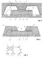
- a first embodiment of the manufacturing process and sensor according to the invention is described by reference to Figs. 1 to 6 .
- This embodiment relates to a sensor that is a temperature sensor as well as a humidity sensor.
- a plurality of sensor chips is manufactured simultaneously on a wafer 1.
- Fig. 1 shows a single chip 5 in detail.
- Each chip may e.g. be a humidity sensor as it is described in US 6 690 569 with a band gap temperature sensor 3 integrated on a first surface 5a thereof.
- Sensitive structure 2 may e.g. be the polymer film of a humidity sensor with underlying electrodes as described in US 6 690 569 .
- further circuitry may be integrated on chip 5, such as analog amplifiers, analog-digital converts and digital processing electronics.
- bond pads 4 are provided on first surface 5a for connecting the band gap circuit and any other circuitry to bond wires.
- Buffer layer 6 is advantageously a photoresist, such as SU-8 by MicroChem Corp., USA. Using a photoresist layer as buffer layer 6 has the advantage that it can be structured easily using standardized processing steps.
- buffer layer 6 is a photoresist, it can be structured directly by means of photolithography in order to remove it at least partially at the location of sensitive structure 2 as well as at the location of the bond pads 4, as shown in Fig. 3 , while leaving it to cover at least band gap circuit 3.
- buffer layer 6 is removed to uncover the contact pads 4 and at least part of sensitive structure 2.
- buffer layer 6 does not cover the contact pads 4 such that the contact pads 4 can later be contacted by the bond wires.
- buffer layer 6 extend over all of sensitive structure 2, but surrounds it, such that said structure can later be exposed to the environment. All steps up to this point can be carried out prior to cutting wafer 1.
- wafer 1 is cut into the chips 5, and a plurality of the chips 5 are placed on a lead frame 7 in known manner, as shown in Fig. 4 .
- the chips 5 may e.g. be glued to the lead frame 7.
- Bond wires 13 are mounted between the contact pads 4 and the leads 7a of lead frame 7.
- lead frame 7 is placed in a mold comprising a lid 8 and a base 9.
- the mold defines an interior space 10 to be filled by a hardening material.
- Lid 8 has a section 11 that extends into interior space 10. Section 11 is located and dimensioned such that, when the mold is closed, it abuts against buffer layer 6 along a circumference of sensitive structure 2, thereby forming a sealed cavity 12 over sensitive structure 2.
- a foil assisted molding process can be used.
- a film 14 is placed over at least one of the parts of mold 8, 9 on the side facing interior space 10.
- Film 14 may e.g. be a ETFE film having a thickness between 50 and 100 ⁇ m.
- a suitable example of such a film is Nowoflon ET6235J by Nowofol, Siegsdorf (Germany) or Fluon by Asahi Glass Co., Japan.
- Such a foil compensates mechanical tolerances, reduces the wear of the mold and simplifies the removal of the mold after the casting process.
- base 9 can be covered by a polyester foil.
- a suitable polyester foil is e.g. RM4100 by Hitachi Chemicals, Japan.
- a hardening material is introduced into the mold to fill interior space 10.
- mold 8 9 is removed, thereby forming the substantially completed device as shown in Fig. 6 .
- section 11 has formed an access opening 15 that connects sensitive structure 2 with the surroundings of the device.
- buffer layer 6 is formed such that it covers bandgap circuit 3 in order to protect it from mechanical stress, such as strain.
- buffer layer 6 advantageously has the following properties:
- buffer layer 6 is advantageously a photoresist, it can also be any other polymer, such as a resin system, e.g. epoxy, in particular a photostructurable resin system such that it can be structured easily. Resin systems have been found to be compatible with the materials that are usually used for injection-molded semiconductor device packaging.
- buffer layer 6 may e.g. also be or comprise a rubber, e.g. silicone rubber, or polyimide. If it is not a photoresist, a separate photoresist layer can e.g. be placed on top of it, which then can be structured to form a mask for subsequently etching the buffer layer at the desired locations.
- a separate photoresist layer can e.g. be placed on top of it, which then can be structured to form a mask for subsequently etching the buffer layer at the desired locations.
- buffer layer 6 may also be applied using printing techniques, such as stencil printing or screen printing, in particular if buffer layer 6 is a silicone rubber.
- buffer layer 6 not only serves to provide a seal with section 11 in the molding process, but it also protects the bandgap circuit 3 from strain. Hence, it is structured such that it covers substantially all of bandgap circuit 3.
- buffer layer 6 can be used not only as a contact surface for section 11 of the mold, but also as a stress relief layer.
- Fig. 7 shows an embodiment of bandgap circuit 3.
- a constant reference voltage can be obtained at output V1, while the voltage difference between outputs V1 and V2 is a measure of the temperature.
- the present invention can also be carried out on temperature sensors without a sensitive structure 2, i.e. on sensors that measure temperature alone.
- the second embodiment shown in Fig. 8 is such a temperature sensor. It differs from the one of Fig. 6 in that all of the first surface 5a of chip 5 is covered by housing 16 and there is no access opening provided therein.
- buffer layer 6 covers substantially all of first surface 5a with the exception of the contact pads 4. At least, it should cover substantially all of bandgap circuit 3.
- the method for manufacturing the second embodiment of Fig. 8 is substantially the same as for manufacturing the first embodiment of Fig. 6 , with the exception that lid 8 has no section 11 extending into interior space 10.
- a temperature sensor with a bandgap circuit 3 is provided.
- Bandgap circuit 3 is covered by a buffer layer 6 of e.g. photoresist.
- Buffer layer 6 is structured and semiconductor chip 5 is packaged in or at least covered by a housing 16.
- mechanical stress as it is e.g. caused by different thermal expansion coefficients of the packaging and the chip, can be reduced.
- the temperature sensor can be an all-solid, monolithic device.
- it advantageously does not comprise a MEMS (a micro electromechanical system), including an IMEMS (an integrated MEMS), as e.g. described in US 6 379 988 .
Abstract
Description
- This application claims the priority of European patent application
08014276.3, filed August 11, 2008 - The invention relates to a temperature sensor and a method for manufacturing the same. In particular it relates to a temperature sensor comprising a semiconductor chip, a bandgap circuit integrated on a first surface of said chip, and a housing for embedding the chip.
- It has been known to provide temperature sensors based on semiconductor chips with bandgap circuits integrated thereon. Such temperature sensors are typically covered by a housing. It has been found that such sensors can be subject to drift and inaccuracies.
- It is an object of the present invention to provide a temperature sensor and a method for its manufacture that provides improved accuracy.
- This object is achieved by the sensor and method of the independent claims. Accordingly, a buffer layer of a polymer is applied to the semiconductor chip and covers the bandgap circuit. Hence, the buffer layer is arranged between the bandgap circuit and the material of the housing. This arrangement prevents mechanical strain from being transferred between housing and bandgap circuit. Since the voltage of the bandgap circuit depends not only on temperature, but also on mechanical stress, the buffer layer improves the accuracy of the device.
- Advantageously, the buffer layer is made of a photoresist. This is a material that can be structured using photolithography, or the product of such a material after structuring by means of photolithography. For example, the buffer layer can comprise an epoxy-based photoresist, in particular SU-8.
- The temperature sensor can further comprise an integrated sensitive structure, such as a polymer film for measuring humidity, in which case the housing can be provided with an access opening extending to the integrated sensitive structure. Thus, the temperature sensor can further measure humidity or some other parameter of the environment.
- Alternatively, the housing can cover the whole of the first surface of the chip, i.e. of the surface on which the bandgap circuit has been integrated.
- Other advantageous embodiments are described in the dependent claims as well as in the following description, wherein the description refers to the attached figures. These show:
-
Fig. 1 a first step in a manufacturing process of a first embodiment of the sensor, prior to applying the buffer layer, -
Fig. 2 a second step, after applying the buffer layer, -
Fig. 3 a third step, after structuring the buffer layer, -
Fig. 4 a fourth step, after cutting the wafer and applying the chip to the lead frame, -
Fig. 5 a fifth step prior to casting, -
Fig. 6 a sixth step, after removing the mold, -
Fig. 7 a reference voltage generator and temperature sensor, and -
Fig. 8 is a second embodiment of a sensor. - In the following, a first embodiment of the manufacturing process and sensor according to the invention is described by reference to
Figs. 1 to 6 . This embodiment relates to a sensor that is a temperature sensor as well as a humidity sensor. - In a first step, a plurality of sensor chips is manufactured simultaneously on a
wafer 1.Fig. 1 shows asingle chip 5 in detail. Each chip may e.g. be a humidity sensor as it is described inUS 6 690 569 with a bandgap temperature sensor 3 integrated on afirst surface 5a thereof. Or it may be any other type of sensor having asensitive structure 2 and aband gap circuit 3 integrated on itsfirst surface 5a.Sensitive structure 2 may e.g. be the polymer film of a humidity sensor with underlying electrodes as described inUS 6 690 569 . In addition to a bandgap temperature sensor 3, further circuitry may be integrated onchip 5, such as analog amplifiers, analog-digital converts and digital processing electronics. - Furthermore,
bond pads 4 are provided onfirst surface 5a for connecting the band gap circuit and any other circuitry to bond wires. - In a next step, a
buffer layer 6 is applied overwafer 1.Buffer layer 6 is advantageously a photoresist, such as SU-8 by MicroChem Corp., USA. Using a photoresist layer asbuffer layer 6 has the advantage that it can be structured easily using standardized processing steps. - If
buffer layer 6 is a photoresist, it can be structured directly by means of photolithography in order to remove it at least partially at the location ofsensitive structure 2 as well as at the location of thebond pads 4, as shown inFig. 3 , while leaving it to cover at leastband gap circuit 3. - Thus,
buffer layer 6 is removed to uncover thecontact pads 4 and at least part ofsensitive structure 2. In other words,buffer layer 6 does not cover thecontact pads 4 such that thecontact pads 4 can later be contacted by the bond wires. Neither doesbuffer layer 6 extend over all ofsensitive structure 2, but surrounds it, such that said structure can later be exposed to the environment. All steps up to this point can be carried out prior to cuttingwafer 1. - Now,
wafer 1 is cut into thechips 5, and a plurality of thechips 5 are placed on alead frame 7 in known manner, as shown inFig. 4 . Thechips 5 may e.g. be glued to thelead frame 7.Bond wires 13 are mounted between thecontact pads 4 and theleads 7a oflead frame 7. - In a next step,
lead frame 7 is placed in a mold comprising alid 8 and abase 9. The mold defines aninterior space 10 to be filled by a hardening material.Lid 8 has asection 11 that extends intointerior space 10.Section 11 is located and dimensioned such that, when the mold is closed, it abuts againstbuffer layer 6 along a circumference ofsensitive structure 2, thereby forming a sealedcavity 12 oversensitive structure 2. - As shown in
Fig. 5 , a foil assisted molding process can be used. In such a process, afilm 14 is placed over at least one of the parts ofmold interior space 10.Film 14 may e.g. be a ETFE film having a thickness between 50 and 100 µm. A suitable example of such a film is Nowoflon ET6235J by Nowofol, Siegsdorf (Germany) or Fluon by Asahi Glass Co., Japan. Such a foil compensates mechanical tolerances, reduces the wear of the mold and simplifies the removal of the mold after the casting process. Similarly,base 9 can be covered by a polyester foil. A suitable polyester foil is e.g. RM4100 by Hitachi Chemicals, Japan. - In a next step, a hardening material is introduced into the mold to fill
interior space 10. - After hardening the material at least partially in order to form a package or
housing 16 that covers and/or surroundschip 5,mold Fig. 6 . As can be seen,section 11 has formed an access opening 15 that connectssensitive structure 2 with the surroundings of the device. - According to the present invention,
buffer layer 6 is formed such that it coversbandgap circuit 3 in order to protect it from mechanical stress, such as strain. - For providing a good mechanical protection during molding and thereafter, and in order to avoid a damage of
sensitive structure 2 during the molding process,buffer layer 6 advantageously has the following properties: - Its height should be sufficient such that
film 14 is prevented from touchingsensitive structure 2 during the molding process. Advantageously, the height ofbuffer layer 6 is at least 10 µm. - It should be sufficiently elastic in order to form a good seal during the molding process and in order to be able to accommodate for mutual movements between
housing 16 and thecircuitry semiconductor chip 5. In particular, and even for embodiments that do not comprise asensitive structure 2, such as the second embodiment described below, it should be more elastic than normal cover layers applied over semiconductor chips, in particular SiN and SiO2. In particular,buffer layer 6 should have a Young's module of less than 10 GPa, which is clearly smaller than the Young's modules of SiN (> 150 GPa) and SiO2 (> 70 GPa). - While, as described above,
buffer layer 6 is advantageously a photoresist, it can also be any other polymer, such as a resin system, e.g. epoxy, in particular a photostructurable resin system such that it can be structured easily. Resin systems have been found to be compatible with the materials that are usually used for injection-molded semiconductor device packaging. - Alternatively,
buffer layer 6 may e.g. also be or comprise a rubber, e.g. silicone rubber, or polyimide. If it is not a photoresist, a separate photoresist layer can e.g. be placed on top of it, which then can be structured to form a mask for subsequently etching the buffer layer at the desired locations. - Alternatively,
buffer layer 6 may also be applied using printing techniques, such as stencil printing or screen printing, in particular ifbuffer layer 6 is a silicone rubber. - As mentioned,
buffer layer 6 not only serves to provide a seal withsection 11 in the molding process, but it also protects thebandgap circuit 3 from strain. Hence, it is structured such that it covers substantially all ofbandgap circuit 3. - This is based on the understanding that mechanical stress strongly affects the properties of semiconductor electronic components, while, at the same time,
buffer layer 6 can be used not only as a contact surface forsection 11 of the mold, but also as a stress relief layer. -
Fig. 7 shows an embodiment ofbandgap circuit 3. A constant reference voltage can be obtained at output V1, while the voltage difference between outputs V1 and V2 is a measure of the temperature. - The present invention can also be carried out on temperature sensors without a
sensitive structure 2, i.e. on sensors that measure temperature alone. The second embodiment shown inFig. 8 is such a temperature sensor. It differs from the one ofFig. 6 in that all of thefirst surface 5a ofchip 5 is covered byhousing 16 and there is no access opening provided therein. - In this embodiment,
buffer layer 6 covers substantially all offirst surface 5a with the exception of thecontact pads 4. At least, it should cover substantially all ofbandgap circuit 3. - The method for manufacturing the second embodiment of
Fig. 8 is substantially the same as for manufacturing the first embodiment ofFig. 6 , with the exception thatlid 8 has nosection 11 extending intointerior space 10. - Hence, in summary, a temperature sensor with a
bandgap circuit 3 is provided.Bandgap circuit 3 is covered by abuffer layer 6 of e.g. photoresist.Buffer layer 6 is structured andsemiconductor chip 5 is packaged in or at least covered by ahousing 16. By providing thebuffer layer 6, mechanical stress, as it is e.g. caused by different thermal expansion coefficients of the packaging and the chip, can be reduced. - The temperature sensor can be an all-solid, monolithic device. In particular, it advantageously does not comprise a MEMS (a micro electromechanical system), including an IMEMS (an integrated MEMS), as e.g. described in
US 6 379 988 - While there are shown and described presently preferred embodiments of the invention, it is to be distinctly understood that the invention is not limited thereto but may be otherwise variously embodied and practised within the scope of the following claims.
Claims (13)
- A temperature sensor comprisinga semiconductor chip (5),a bandgap circuit (3) integrated on a first surface (5a) of said semiconductor chip (5), anda housing (16), with said semiconductor chip (5) being covered by said housing (16),characterized in that said temperature sensor further comprises a polymer buffer layer (6) applied to said semiconductor chip (5) and covering said bandgap circuit (3).
- The temperature sensor of claim 1 wherein said buffer layer is a photoresist.
- The temperature sensor of claim 2 wherein said buffer layer (6) comprises an epoxy-based photoresist.
- The temperature sensor of claim 3 wherein said buffer layer (6) comprises SU-8.
- The temperature sensor of any of the preceding claims wherein said semiconductor chip (5) comprises contact pads (4) wherein said buffer layer (6) does not cover said contact pads (4).
- The temperature sensor of any of the preceding claims further comprising an integrated sensitive structure (2) and wherein said housing (16) comprises an access opening (15) extending to said integrated sensitive structure (2).
- The temperature sensor of claim 6 wherein said integrated sensitive structure is a polymer film for measuring humidity.
- The temperature sensor of any of the claims 6 or 7 wherein said buffer layer (6) does not extend over all of said integrated sensitive structure (2).
- The temperature sensor of any of the claims 2 to 5 wherein said housing (16) covers the whole of said first surface (5a) of said chip (5).
- The temperature sensor of any of the preceding claims not comprising a MEMS device.
- A method for manufacturing a temperature sensor comprising a semiconductor chip (5) with a band gap circuit integrated thereon, said method comprising the steps ofapplying, onto a first surface (5a) of said chip (5), a photoresist buffer layer (6),lithographically structuring said buffer layer (6) in order to remove part of said buffer layer but leaving said buffer layer covering said bandgap circuit (3),casting a housing (16) over said chip (5), with said housing (16) covering said buffer layer (6).
- The method of claim 11 wherein said chip further comprises an integrated sensitive structure (2), and wherein said method further comprises the steps of
structuring said buffer layer (6) such that at least part of said sensitive structure (2) is uncovered,
providing a mold (8, 9) defining an interior space (10) and having a section (11) extending into said interior space (10),
placing said chip (5) in said mold (8, 9) with said section (11) abutting against said buffer layer (6),
introducing a hardening material into said mold (8, 9) for casting said housing (16) over said chip,
after hardening said material at least partially, removing said section (11) thereby forming an access opening (15) extending to said sensitive structure (2). - The method of any of the claims 10 or 12 comprising the steps of
manufacturing a plurality of said chips (5) together on a single wafer (1),
applying said buffer layer (6) to said wafer,
lithographically structuring said buffer layer (6) and, thereafter,
cutting said wafer (1) into said chips (5).
Priority Applications (1)
| Application Number | Priority Date | Filing Date | Title |
|---|---|---|---|
| EP09009135A EP2154714A3 (en) | 2008-08-11 | 2009-07-14 | Temperature sensor with buffer layer |
Applications Claiming Priority (2)
| Application Number | Priority Date | Filing Date | Title |
|---|---|---|---|
| EP08014276A EP2154713B1 (en) | 2008-08-11 | 2008-08-11 | Method for manufacturing a sensor device with a stress relief layer |
| EP09009135A EP2154714A3 (en) | 2008-08-11 | 2009-07-14 | Temperature sensor with buffer layer |
Publications (2)
| Publication Number | Publication Date |
|---|---|
| EP2154714A2 true EP2154714A2 (en) | 2010-02-17 |
| EP2154714A3 EP2154714A3 (en) | 2010-03-24 |
Family
ID=40289356
Family Applications (2)
| Application Number | Title | Priority Date | Filing Date |
|---|---|---|---|
| EP08014276A Active EP2154713B1 (en) | 2008-08-11 | 2008-08-11 | Method for manufacturing a sensor device with a stress relief layer |
| EP09009135A Withdrawn EP2154714A3 (en) | 2008-08-11 | 2009-07-14 | Temperature sensor with buffer layer |
Family Applications Before (1)
| Application Number | Title | Priority Date | Filing Date |
|---|---|---|---|
| EP08014276A Active EP2154713B1 (en) | 2008-08-11 | 2008-08-11 | Method for manufacturing a sensor device with a stress relief layer |
Country Status (4)
| Country | Link |
|---|---|
| US (2) | US20100117185A1 (en) |
| EP (2) | EP2154713B1 (en) |
| JP (1) | JP5623038B2 (en) |
| CN (1) | CN101667548A (en) |
Cited By (1)
| Publication number | Priority date | Publication date | Assignee | Title |
|---|---|---|---|---|
| WO2012100362A1 (en) * | 2011-01-27 | 2012-08-02 | Sensirion Ag | Method for manufacturing a sensor chip |
Families Citing this family (41)
| Publication number | Priority date | Publication date | Assignee | Title |
|---|---|---|---|---|
| EP2154713B1 (en) | 2008-08-11 | 2013-01-02 | Sensirion AG | Method for manufacturing a sensor device with a stress relief layer |
| EP2224218B1 (en) * | 2009-02-25 | 2018-11-28 | Sensirion Automotive Solutions AG | A sensor in a moulded package and a method for manufacturing the same |
| WO2010113712A1 (en) * | 2009-03-31 | 2010-10-07 | アルプス電気株式会社 | Capacitance type humidity sensor and method for manufacturing same |
| DE102010033963A1 (en) * | 2010-08-11 | 2012-02-16 | Osram Opto Semiconductors Gmbh | Optoelectronic component and method for producing an optoelectronic component |
| DE102011004381A1 (en) * | 2011-02-18 | 2012-08-23 | Robert Bosch Gmbh | Mold module with sensor element |
| DE102011013468A1 (en) * | 2011-03-09 | 2012-09-13 | Micronas Gmbh | Semiconductor package and method of manufacturing a semiconductor package |
| EP2573804A1 (en) * | 2011-09-21 | 2013-03-27 | Nxp B.V. | Integrated circuit with sensor and manufacturing method thereof |
| JP5708688B2 (en) * | 2012-08-27 | 2015-04-30 | 株式会社デンソー | Manufacturing method of sensor package |
| JP6018903B2 (en) | 2012-12-17 | 2016-11-02 | 日立オートモティブシステムズ株式会社 | Physical quantity sensor |
| DE102013217892A1 (en) * | 2012-12-20 | 2014-06-26 | Continental Teves Ag & Co. Ohg | Electronic device and method for manufacturing an electronic device |
| DE102012224424A1 (en) | 2012-12-27 | 2014-07-17 | Robert Bosch Gmbh | Sensor system and cover device for a sensor system |
| US9902162B2 (en) | 2013-02-28 | 2018-02-27 | Hewlett-Packard Development Company, L.P. | Molded print bar |
| EP2961612B1 (en) | 2013-02-28 | 2019-08-07 | Hewlett-Packard Development Company, L.P. | Molding a fluid flow structure |
| US10821729B2 (en) | 2013-02-28 | 2020-11-03 | Hewlett-Packard Development Company, L.P. | Transfer molded fluid flow structure |
| US9724920B2 (en) | 2013-03-20 | 2017-08-08 | Hewlett-Packard Development Company, L.P. | Molded die slivers with exposed front and back surfaces |
| EP2871152B1 (en) | 2013-11-06 | 2017-05-24 | Sensirion AG | Sensor device |
| KR20150074427A (en) * | 2013-12-24 | 2015-07-02 | 삼성전기주식회사 | Sensor package and portable terminal having the same |
| CN108615711A (en) * | 2014-01-24 | 2018-10-02 | 清华大学 | A kind of encapsulating structure and packaging method based on template |
| EP2942807B1 (en) * | 2014-05-07 | 2020-08-26 | Sensirion AG | Semiconductor package |
| EP3001186B1 (en) | 2014-09-26 | 2018-06-06 | Sensirion AG | Sensor chip |
| EP3032227B1 (en) | 2014-12-08 | 2020-10-21 | Sensirion AG | Flow sensor package |
| US9355870B1 (en) | 2015-01-15 | 2016-05-31 | Silicon Laboratories Inc. | Integrated circuit with sensor area and resin dam |
| US20160360622A1 (en) * | 2015-06-02 | 2016-12-08 | Microchip Technology Incorporated | Integrated Circuit With Sensor Printed In Situ |
| EP3168866B1 (en) | 2015-11-16 | 2020-12-30 | ams AG | Semiconductor humidity sensor device and manufacturing method thereof |
| US9781324B2 (en) * | 2016-02-18 | 2017-10-03 | Ningbo Sunny Opotech Co., Ltd. | Array imaging module and molded photosensitive assembly, circuit board assembly and manufacturing methods thereof for electronic device |
| EP3429183A4 (en) * | 2016-03-12 | 2019-12-11 | Ningbo Sunny Opotech Co., Ltd. | Camera module, and photosensitive component thereof and manufacturing method therefor |
| US10908324B2 (en) * | 2016-03-12 | 2021-02-02 | Ningbo Sunny Opotech Co., Ltd. | Molded photosensitive assembly of array imaging module |
| US9899290B2 (en) * | 2016-03-23 | 2018-02-20 | Nxp Usa, Inc. | Methods for manufacturing a packaged device with an extended structure for forming an opening in the encapsulant |
| US9799580B2 (en) * | 2016-03-24 | 2017-10-24 | Nxp Usa, Inc. | Semiconductor device package and methods of manufacture thereof |
| US11289521B2 (en) * | 2016-03-28 | 2022-03-29 | Ningbo Sunny Opotech Co., Ltd. | Camera module and molded photosensitive assembly and manufacturing method therefor, and electronic device |
| CN105681640B (en) * | 2016-03-28 | 2019-12-27 | 宁波舜宇光电信息有限公司 | Camera module and manufacturing method thereof |
| EP3493517B1 (en) * | 2016-08-01 | 2023-05-31 | Ningbo Sunny Opotech Co., Ltd. | Photographing module, molded circuit board assembly and molded photosensitive assembly thereof and manufacturing methods |
| TWM557833U (en) * | 2016-08-01 | 2018-04-01 | Ningbo Sunny Opotech Co Ltd | Camera module, molded photosensitive element, molding die, and its electronic equipment |
| US10659664B2 (en) * | 2016-08-01 | 2020-05-19 | Ningbo Sunny Opotech Co., Ltd. | Camera module and molded circuit board assembly and manufacturing method thereof |
| CN108695165A (en) * | 2017-04-07 | 2018-10-23 | 宁波舜宇光电信息有限公司 | Method for packaging semiconductor based on molding process and semiconductor device |
| WO2018184572A1 (en) * | 2017-04-07 | 2018-10-11 | 宁波舜宇光电信息有限公司 | Molding technique-based semiconductor packaging method and semiconductor device |
| JP6780675B2 (en) | 2017-07-24 | 2020-11-04 | 株式会社デンソー | Semiconductor devices and methods for manufacturing semiconductor devices |
| CN109524372A (en) * | 2018-12-29 | 2019-03-26 | 山东盛品电子技术有限公司 | Encapsulating structure, the method for solving sensor chip encapsulation post package body internal stress |
| WO2021004470A1 (en) * | 2019-07-10 | 2021-01-14 | 宁波舜宇光电信息有限公司 | Preparation method for photosensitive assembly, photosensitive assembly, and photographing module |
| JP7442333B2 (en) | 2020-02-12 | 2024-03-04 | エイブリック株式会社 | Semiconductor device and its manufacturing method |
| US11804416B2 (en) | 2020-09-08 | 2023-10-31 | UTAC Headquarters Pte. Ltd. | Semiconductor device and method of forming protective layer around cavity of semiconductor die |
Citations (2)
| Publication number | Priority date | Publication date | Assignee | Title |
|---|---|---|---|---|
| US6379988B1 (en) | 2000-05-16 | 2002-04-30 | Sandia Corporation | Pre-release plastic packaging of MEMS and IMEMS devices |
| US6690569B1 (en) | 1999-12-08 | 2004-02-10 | Sensirion A/G | Capacitive sensor |
Family Cites Families (45)
| Publication number | Priority date | Publication date | Assignee | Title |
|---|---|---|---|---|
| US2154713A (en) * | 1936-04-17 | 1939-04-18 | Shell Dev | Process for extracting ethereal oils |
| US4620502A (en) * | 1986-01-31 | 1986-11-04 | Kimble Erma N | Hand sanitizer |
| JPS62254451A (en) * | 1986-04-28 | 1987-11-06 | Canon Inc | Electronic part device |
| JPH0724287B2 (en) * | 1987-02-12 | 1995-03-15 | 三菱電機株式会社 | Semiconductor device having light transmitting window and method of manufacturing the same |
| US4888988A (en) * | 1987-12-23 | 1989-12-26 | Siemens-Bendix Automotive Electronics L.P. | Silicon based mass airflow sensor and its fabrication method |
| US5026667A (en) * | 1987-12-29 | 1991-06-25 | Analog Devices, Incorporated | Producing integrated circuit chips with reduced stress effects |
| JPH02227485A (en) | 1989-02-28 | 1990-09-10 | Mitsubishi Electric Corp | Sealing material for semiconductor |
| SE469415B (en) * | 1991-11-21 | 1993-07-05 | Rollen Jarl Erik | PROCEDURES AND RESOURCES TO ESTABLISH AND MAKE A MICROBIOLOGY CLEAN SPACE ENVIRONMENT |
| US5332469A (en) * | 1992-11-12 | 1994-07-26 | Ford Motor Company | Capacitive surface micromachined differential pressure sensor |
| NL9400766A (en) * | 1994-05-09 | 1995-12-01 | Euratec Bv | Method for encapsulating an integrated semiconductor circuit. |
| NL1003315C2 (en) * | 1996-06-11 | 1997-12-17 | Europ Semiconductor Assembly E | Method for encapsulating an integrated semiconductor circuit. |
| HUP0004231A2 (en) * | 1997-07-31 | 2001-03-28 | Procter & Gamble | Wet-like cleaning articles |
| US6313049B1 (en) * | 1998-05-04 | 2001-11-06 | Dotty Heady | Disposable fabric-saturated sanitizer wipe(s) for food industry with sealed container packaging therefor |
| NL1011929C2 (en) * | 1999-04-29 | 2000-10-31 | 3P Licensing Bv | Method for encapsulating electronic components, in particular integrated circuits. |
| DE19929025A1 (en) | 1999-06-25 | 2000-12-28 | Bosch Gmbh Robert | Pressures sensor has moulded housing, pressure channel to semiconducting pressure transducer formed by interior vol. of cap formed by cap upper side, cap wall and opening |
| EP1236037B1 (en) * | 1999-11-30 | 2007-10-10 | Sensirion AG | Sensor accommodated in a housing |
| US6489178B2 (en) * | 2000-01-26 | 2002-12-03 | Texas Instruments Incorporated | Method of fabricating a molded package for micromechanical devices |
| AT410727B (en) * | 2000-03-14 | 2003-07-25 | Austria Mikrosysteme Int | METHOD FOR PLACING SENSORS IN A HOUSING |
| CH695166A5 (en) * | 2000-04-25 | 2005-12-30 | Sensirion Ag | Method and apparatus for measuring the flow of a liquid. |
| US6794352B2 (en) * | 2000-06-12 | 2004-09-21 | Jeffrey S. Svendsen | Cleaning towel having a color identifying label and sanitizer release polymer composition |
| US6729181B2 (en) * | 2000-08-23 | 2004-05-04 | Sensiron Ag | Flow sensor in a housing |
| NL1018403C1 (en) | 2000-10-05 | 2002-04-08 | Boschman Tech Bv | Method for cutting a composite structure with one or more electronic components using a laser. |
| EP1211722B9 (en) | 2000-11-30 | 2005-07-13 | STMicroelectronics S.r.l. | Manufacturing method of electronic device package |
| EP1220309A1 (en) * | 2000-12-28 | 2002-07-03 | STMicroelectronics S.r.l. | Manufacturing method of an electronic device package |
| EP1350078B1 (en) * | 2001-01-10 | 2018-02-14 | Sensirion Holding AG | Micromechanical flow sensor with a tensile coating |
| EP1246235A1 (en) * | 2001-03-26 | 2002-10-02 | European Semiconductor Assembly (Eurasem) B.V. | Method for encapsulating a chip having a sensitive surface |
| NL1019042C2 (en) * | 2001-09-26 | 2003-03-27 | Europ Semiconductor Assembly E | Method for encapsulating a chip and / or other object. |
| JP3882592B2 (en) * | 2001-11-26 | 2007-02-21 | 松下電工株式会社 | Semiconductor ion sensor and manufacturing method thereof |
| US20030191692A1 (en) * | 2002-04-05 | 2003-10-09 | Vogel Philip S. | Method for a restaurant to do business including the step of providing hand sanitizer to customers |
| US7109574B2 (en) * | 2002-07-26 | 2006-09-19 | Stmicroelectronics, Inc. | Integrated circuit package with exposed die surfaces and auxiliary attachment |
| GB0307616D0 (en) * | 2003-04-02 | 2003-05-07 | Melexis Nv | Calorimetric flow meter |
| TW200522292A (en) * | 2003-12-31 | 2005-07-01 | Advanced Semiconductor Eng | Chip package sturcture |
| JP2004266844A (en) * | 2004-03-26 | 2004-09-24 | Mitsubishi Electric Corp | Imaging unit and manufacturing method thereof |
| EP1628132B1 (en) * | 2004-08-17 | 2015-01-07 | Sensirion Holding AG | Method and device for calibrating sensors |
| US20060153733A1 (en) * | 2005-01-10 | 2006-07-13 | Simon Sassoon | Door handle sanitizer system and apparatus |
| US7067350B1 (en) * | 2005-01-31 | 2006-06-27 | Taiwan Semiconductor Manufacturing Company, Ltd. | Method of manufacturing a semiconductor device using electrical contacts formed in an isolation layer |
| WO2006114005A1 (en) | 2005-04-27 | 2006-11-02 | Sensirion Ag | A method for packaging integrated sensors |
| US20060289558A1 (en) * | 2005-06-28 | 2006-12-28 | Parker Kimberly A | Publicly-accessible moist hand cleaning wipe station |
| DE102005047856B4 (en) * | 2005-10-05 | 2007-09-06 | Infineon Technologies Ag | Semiconductor component with semiconductor device components embedded in a plastic housing composition, system carrier for accommodating the semiconductor device components and method for producing the system carrier and semiconductor components |
| EP1873499A1 (en) | 2006-06-30 | 2008-01-02 | Sensirion AG | Thermal flow sensor for high flow velocities |
| DE112006004083T5 (en) * | 2006-10-18 | 2009-11-26 | Sensirion Holding Ag | Method for packaging integrated sensors |
| US20080193495A1 (en) * | 2007-02-14 | 2008-08-14 | Maryam Yousefi Kharazmi | Disposable hand sanitizer gel dispenser |
| US20080258318A1 (en) * | 2007-04-20 | 2008-10-23 | Nec Electronics Corporation | Semiconductor device |
| JP2009081346A (en) * | 2007-09-27 | 2009-04-16 | Panasonic Corp | Optical device and method for manufacturing same |
| EP2154713B1 (en) * | 2008-08-11 | 2013-01-02 | Sensirion AG | Method for manufacturing a sensor device with a stress relief layer |
-
2008
- 2008-08-11 EP EP08014276A patent/EP2154713B1/en active Active
-
2009
- 2009-07-14 US US12/460,152 patent/US20100117185A1/en not_active Abandoned
- 2009-07-14 EP EP09009135A patent/EP2154714A3/en not_active Withdrawn
- 2009-08-05 US US12/462,528 patent/US7901971B2/en active Active
- 2009-08-10 JP JP2009185388A patent/JP5623038B2/en active Active
- 2009-08-11 CN CN200910173376A patent/CN101667548A/en active Pending
Patent Citations (2)
| Publication number | Priority date | Publication date | Assignee | Title |
|---|---|---|---|---|
| US6690569B1 (en) | 1999-12-08 | 2004-02-10 | Sensirion A/G | Capacitive sensor |
| US6379988B1 (en) | 2000-05-16 | 2002-04-30 | Sandia Corporation | Pre-release plastic packaging of MEMS and IMEMS devices |
Cited By (1)
| Publication number | Priority date | Publication date | Assignee | Title |
|---|---|---|---|---|
| WO2012100362A1 (en) * | 2011-01-27 | 2012-08-02 | Sensirion Ag | Method for manufacturing a sensor chip |
Also Published As
| Publication number | Publication date |
|---|---|
| JP2010050452A (en) | 2010-03-04 |
| CN101667548A (en) | 2010-03-10 |
| EP2154713B1 (en) | 2013-01-02 |
| EP2154714A3 (en) | 2010-03-24 |
| EP2154713A1 (en) | 2010-02-17 |
| US7901971B2 (en) | 2011-03-08 |
| JP5623038B2 (en) | 2014-11-12 |
| US20100117185A1 (en) | 2010-05-13 |
| US20100035373A1 (en) | 2010-02-11 |
Similar Documents
| Publication | Publication Date | Title |
|---|---|---|
| EP2154714A2 (en) | Temperature sensor with buffer layer | |
| US11192777B2 (en) | MEMS sensor package systems and methods | |
| US7880244B2 (en) | Wafer level CSP sensor | |
| US9105649B2 (en) | Semiconductor component and corresponding production method | |
| WO2011062242A1 (en) | Sensor device and method of manufacture thereof | |
| WO2012100362A1 (en) | Method for manufacturing a sensor chip | |
| US9731959B2 (en) | Integrated device packages having a MEMS die sealed in a cavity by a processor die and method of manufacturing the same | |
| US9981843B2 (en) | Chip package and a method of producing the same | |
| CN105470212A (en) | Packages for semiconductor devices and methods for assembling same | |
| US7617599B2 (en) | Sensor packaging method for a human contact interface | |
| JP4675945B2 (en) | Semiconductor device | |
| JP2007189032A (en) | Manufacturing method of semiconductor device with sealed space | |
| CN111664966B (en) | Pressure sensor for stress decoupling on flexible substrate | |
| US11655142B2 (en) | Method of manufacturing a sensor device and moulding support structure | |
| US10858245B2 (en) | Deposition of protective material at wafer level in front end for early stage particle and moisture protection | |
| EP3601957B1 (en) | Sensor package | |
| Shaw et al. | Package design of pressure sensors for high volume consumer applications | |
| US11823968B2 (en) | Semiconductor device package having stress isolation and method therefor | |
| CN111646424B (en) | Mechanical stress decoupling of microelectromechanical system (MEMS) elements with gel filling | |
| EP2287596A1 (en) | Sensor with glob-top and method for manufacturing the same |
Legal Events
| Date | Code | Title | Description |
|---|---|---|---|
| PUAI | Public reference made under article 153(3) epc to a published international application that has entered the european phase |
Free format text: ORIGINAL CODE: 0009012 |
|
| AK | Designated contracting states |
Kind code of ref document: A2 Designated state(s): AT BE BG CH CY CZ DE DK EE ES FI FR GB GR HR HU IE IS IT LI LT LU LV MC MK MT NL NO PL PT RO SE SI SK SM TR |
|
| AX | Request for extension of the european patent |
Extension state: AL BA RS |
|
| PUAL | Search report despatched |
Free format text: ORIGINAL CODE: 0009013 |
|
| AK | Designated contracting states |
Kind code of ref document: A3 Designated state(s): AT BE BG CH CY CZ DE DK EE ES FI FR GB GR HR HU IE IS IT LI LT LU LV MC MK MT NL NO PL PT RO SE SI SK SM TR |
|
| AX | Request for extension of the european patent |
Extension state: AL BA RS |
|
| STAA | Information on the status of an ep patent application or granted ep patent |
Free format text: STATUS: THE APPLICATION IS DEEMED TO BE WITHDRAWN |
|
| 18D | Application deemed to be withdrawn |
Effective date: 20100925 |