EP2152049A1 - System for transmitting a signal, in particular a differential signal - Google Patents
System for transmitting a signal, in particular a differential signal Download PDFInfo
- Publication number
- EP2152049A1 EP2152049A1 EP08305459A EP08305459A EP2152049A1 EP 2152049 A1 EP2152049 A1 EP 2152049A1 EP 08305459 A EP08305459 A EP 08305459A EP 08305459 A EP08305459 A EP 08305459A EP 2152049 A1 EP2152049 A1 EP 2152049A1
- Authority
- EP
- European Patent Office
- Prior art keywords
- paths
- path
- pair
- distance
- signal
- Prior art date
- Legal status (The legal status is an assumption and is not a legal conclusion. Google has not performed a legal analysis and makes no representation as to the accuracy of the status listed.)
- Granted
Links
Images


Classifications
-
- H—ELECTRICITY
- H05—ELECTRIC TECHNIQUES NOT OTHERWISE PROVIDED FOR
- H05K—PRINTED CIRCUITS; CASINGS OR CONSTRUCTIONAL DETAILS OF ELECTRIC APPARATUS; MANUFACTURE OF ASSEMBLAGES OF ELECTRICAL COMPONENTS
- H05K1/00—Printed circuits
- H05K1/02—Details
- H05K1/0213—Electrical arrangements not otherwise provided for
- H05K1/0237—High frequency adaptations
- H05K1/0245—Lay-out of balanced signal pairs, e.g. differential lines or twisted lines
-
- H—ELECTRICITY
- H01—ELECTRIC ELEMENTS
- H01P—WAVEGUIDES; RESONATORS, LINES, OR OTHER DEVICES OF THE WAVEGUIDE TYPE
- H01P3/00—Waveguides; Transmission lines of the waveguide type
- H01P3/02—Waveguides; Transmission lines of the waveguide type with two longitudinal conductors
- H01P3/026—Coplanar striplines [CPS]
-
- H—ELECTRICITY
- H05—ELECTRIC TECHNIQUES NOT OTHERWISE PROVIDED FOR
- H05K—PRINTED CIRCUITS; CASINGS OR CONSTRUCTIONAL DETAILS OF ELECTRIC APPARATUS; MANUFACTURE OF ASSEMBLAGES OF ELECTRICAL COMPONENTS
- H05K1/00—Printed circuits
- H05K1/02—Details
- H05K1/0213—Electrical arrangements not otherwise provided for
- H05K1/0216—Reduction of cross-talk, noise or electromagnetic interference
- H05K1/0228—Compensation of cross-talk by a mutually correlated lay-out of printed circuit traces, e.g. for compensation of cross-talk in mounted connectors
-
- H—ELECTRICITY
- H05—ELECTRIC TECHNIQUES NOT OTHERWISE PROVIDED FOR
- H05K—PRINTED CIRCUITS; CASINGS OR CONSTRUCTIONAL DETAILS OF ELECTRIC APPARATUS; MANUFACTURE OF ASSEMBLAGES OF ELECTRICAL COMPONENTS
- H05K2201/00—Indexing scheme relating to printed circuits covered by H05K1/00
- H05K2201/09—Shape and layout
- H05K2201/09209—Shape and layout details of conductors
- H05K2201/09218—Conductive traces
- H05K2201/09236—Parallel layout
Definitions
- the invention relates to the systems for transmitting signals, in particular differential signals.
- a differential signal is a signal built from two complementary signals sent on two separate electrically conductive elements, for instance paths of a printed circuit board.
- the two complementary signals are transmitted from an emitting element to a receiving element which reads the difference between the two complementary signals, corresponding to the differential signal.
- the paths that transmit the complementary signals constitute a pair of paths.
- a signal transmitted in a path generates in an other path a noise signal that perturbs the transmission of the main signal - i.e. the signal containing information - by this path.
- This phenomenon is called "crosstalk noise”.
- the noise signal generated by paths of a first pair in paths of a second pair can perturb the differential signal originated from the second pair.
- the arrangement of the paths relative to each other in particular the distance between the path of the first pair and each of the path of the second pair, can be chosen so that the perturbation due to the crosstalk noise of the differential signal transmitted by the second pair is very little, and even null.
- the system of the invention is not aimed at diminishing the noise signal generated by the paths of the first pair in the paths of the second pair but enables to compensate the noise signal generated by the paths of the first pair in each path of the second pair.
- Distances between the paths are preferably chosen so that a noise signal generated by the paths from the first, respectively the second, pair in one of the paths of the second, respectively the first, pair is the same as a noise signal generated by the paths from the first, respectively the second, pair in the other path of the second, respectively the first, pair.
- Each external path and the internal path which is not adjacent to the external path can form a pair of paths able to transmit a differential signal.
- the printed circuit board 10 is realized in an electrically insulating material, such as plastic material, for instance epoxy resin. It comprises four rows of vias 11. These vias 11 are configured to receive connecting pins (not represented) of at least a device, the connecting pins being press-fitted in the vias 11. The connecting pins go through the vias of every layer of the backplane.
- the paths 12, 14 constitute a first pair of paths that transmit a first differential signal, called TX, from a first device (not represented), for instance an Ethernet switch, connected to the second row 16A of connectors to a second device (not represented), for instance a graphic card, connected to the third row 16B of connectors.
- TX first differential signal
- the differential signal TX is constituted by the signal transmitted by the path 12 to which is substracted the signal transmitted by the path 14.
- the signals received from the paths 12, 14 are handled by the second device to reconstitute the differential signal TX.
- the paths 13, 15 constitute a second pair of paths that transmit a second differential signal, called RX, from the second device to the first device.
- the differential signal RX is constituted by the signal transmitted by the path 15 to which is substracted the signal transmitted by the path 13.
- the signals received from the paths 13, 15 are handled by the first device to reconstitute the differential signal RX.
- the path 12 transmits a signal which is null or positive with an amplitude of +Amp1 Volts, whereas the path 14 transmits a signal which is null or negative with an amplitude of -Amp1 Volts.
- the path 15 transmits a signal which is null or positive with an amplitude of +Amp2 Volts, whereas the path 13 transmits a signal which is null or negative with an amplitude of -Amp2 Volts.
- Path 14 corresponds to a first path
- path 13 corresponds to a second path
- path 15 corresponds to a third path
- path 12 corresponds to a fourth path.
- the paths 12, 15 situated at the extremities of the arrangement are called external paths while paths 13, 14 situated between paths 12, 15 are called internal paths.
- a distance between the paths 12 and 13 is referred to as D 1
- a distance between the paths 13 and 14 is referred to as D 2
- a distance between the paths 14 and 15 is referred to as D 3 .
- distances D 1 and D 3 are equal while distance D 2 is smaller than distances D 1 , D 3 .
- the influence of the crosstalk can therefore be cancelled in the differential signal transmitted by the first pair.
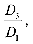
- This arrangement of paths 12 to 15 therefore enables to eliminate the crosstalk noise in the differential signals generated by the pairs of paths 12, 14 and 13, 15. Moreover, as the only parameters to take into account to cancel the crosstalk noise are the ratios of the distances D 2 D 1 and D 3 D 1 , the value of distances D 1 to D 3 does not matter and can be diminished.
- figure 3A is a view analogous to the one of figure 2 , but for a system of the state of the art.
- This system also comprises four paths 20A, 20B, 22A, 22B, which are parallel to each other on most of their length.
- the paths 20A and 20B form a first pair of paths that generates a first differential signal.
- the paths 22A and 22B form a second pair of paths that generates a second differential signal.
- the two paths of a same pair are adjacent and the distance between two paths of a same pair is far smaller than the distance between the path 20B of the first pair and the path 22A of the second pair, these two paths being adjacent.
- the pairs of paths are intentionally spaced away in this system to avoid crosstalk noise in the differential signals generated by these pairs.
- the invention is not limited to the above-mentioned mode of construction.
- the two pairs of paths can lead to distinct devices.
- the ratio of the distance between the two internal paths to the distance between an internal path and an adjacent external path is not set obligatory to 0.5 or between 0.6 to 0.8.
Landscapes
- Engineering & Computer Science (AREA)
- Microelectronics & Electronic Packaging (AREA)
- Physics & Mathematics (AREA)
- Electromagnetism (AREA)
- Cable Transmission Systems, Equalization Of Radio And Reduction Of Echo (AREA)
- Details Of Connecting Devices For Male And Female Coupling (AREA)
Abstract
Description
- The invention relates to the systems for transmitting signals, in particular differential signals.
- A differential signal is a signal built from two complementary signals sent on two separate electrically conductive elements, for instance paths of a printed circuit board. The two complementary signals are transmitted from an emitting element to a receiving element which reads the difference between the two complementary signals, corresponding to the differential signal. The paths that transmit the complementary signals constitute a pair of paths.
- Generally, a system for transmitting differential signals comprises at least two pairs of parallel paths able to transmit a differential signal. For instance, a first pair enables to transmit a differential signal from a first device to a second device and a second pair enables to transmit a differential signal from the second device to the first device.
- It is known that a signal transmitted in a path generates in an other path a noise signal that perturbs the transmission of the main signal - i.e. the signal containing information - by this path. This phenomenon is called "crosstalk noise". In particular, the noise signal generated by paths of a first pair in paths of a second pair can perturb the differential signal originated from the second pair.
- To address this problem, it is known to space away the two pairs of paths on the printed circuit board. The noise signal generated by the first path in the second path indeed diminishes as the distance between these paths increases. As a result, on the printed circuit board, the distance between a path of the first pair and a path of the second pair is far greater than the distance between paths of the same pair.
- The above-mentioned system of the state of the art is satisfying concerning the influence of the crosstalk noise on the differential signals transmitted by the system but not in accordance with the tendency to reduce the dimensions and the complexity of the printed circuit boards. In such a system, the maximum density of interconnection is indeed limited by the great distance that must be set between the paths of each pair.
- An object of the invention is to increase the density of paths on printed circuit boards without increasing the perturbation of the differential signal transmitted in the paths of the first, respectively the second, pair by the signals transmitted by the paths of the second, respectively the first, pair.
- According to the invention, we provide a system for transmitting differential signals, comprising at least first and second pairs of electrically conductive paths, at least a path of the first pair being arranged between the paths of the second pair.
- Thus, the path of the first pair, arranged between the paths of the second pair, generates a noise signal in each path of the second pair. As the differential signal generated by the second pair is constituted by the difference of the signal transmitted by a predetermined path of the second pair, called positive path, and of the signal transmitted by the other path of the second pair, called negative path, the noise signal generated by the path of the first pair in the negative path is substracted from the noise signal generated by the path of the first pair in the positive path.
- The arrangement of the paths relative to each other, in particular the distance between the path of the first pair and each of the path of the second pair, can be chosen so that the perturbation due to the crosstalk noise of the differential signal transmitted by the second pair is very little, and even null.
- As a matter of fact, the system of the invention is not aimed at diminishing the noise signal generated by the paths of the first pair in the paths of the second pair but enables to compensate the noise signal generated by the paths of the first pair in each path of the second pair. Distances between the paths are preferably chosen so that a noise signal generated by the paths from the first, respectively the second, pair in one of the paths of the second, respectively the first, pair is the same as a noise signal generated by the paths from the first, respectively the second, pair in the other path of the second, respectively the first, pair.
- Consequently, the total space taken by the two pairs of paths can be diminished. Thus, the price of the system is also diminished.
- It will be noted that the paths are parallel relative to each other on most of their length, the distances between the paths being easy to measure.
- The system of the invention can also comprise one or more of the characteristics listed below:
- the paths of the first pair are alternated with the paths of the second pair, which enables to diminish the perturbation of the noise signal in both differential signals,
- a first path, belonging to the first pair, is situated between the paths of the second pair and a second path, belonging to the second pair, is situated between the paths of the first pair, a distance between the first and second paths being inferior to a distance between the first path and each of the other paths. Indeed, one of the paths of a pair (for instance, the first path) often transmits a positive signal while the other path (for instance, a path of the first pair referred to as fourth path) transmits a negative signal. The positive noise signal generated by the first path in the second path is greater than the positive noise signal generated by the first path in the other path of the second pair, referred to as third path. The positive noise signal generated in the second path can therefore be partly compensated by the positive noise signal generated in the third path (which is substracted to the noise signal generated in the second path) and partly compensated by the negative noise signal generated by the fourth path in the second path (the influence of the fourth path on the third path being considered as negligible). As a matter of fact, with this kind of arrangement, the influence of the crosstalk noise on the differential signal originated from the second pair can be very little, or even null,
- the distance between the first and second paths can also be inferior to a distance between the second path and each of the other paths. As a matter of fact, with this kind of arrangement, the influence of the crosstalk noise on the differential signal originated from the first pair can be very little, or even null,
- a distance between the first path and a third path, belonging to the second pair, is equal to a distance between the second path and a fourth path, belonging to the first pair. It enables to optimise the cancellation of the crosstalk noise in the differential signals,
- a ratio of the distance between the first and second paths to the distance between the first and third paths is comprised between 0.5 and 1, more particularly between 0.6 and 0.8. This value has been calculated as an ideal value that enables to greatly diminish the crosstalk noise in differential signals, and also to take into account other important parameters of the circuit, such as parameters relative to the controlled impedance,
- a ratio of the distance between the first and second paths to the distance between the second and fourth paths is also preferably comprised between 0.5 and 1, more particularly between 0.6 and 0.8, for the above-mentioned reasons,
- the system comprises at least a printed circuit board presenting the two pairs of paths,
- the system comprises a backplane comprising at least two superposed printed circuit boards, at least one printed circuit board presenting the two pairs of paths. The system is particularly advantageous in this case. Indeed, backplanes comprise several superposed layers of printed board circuit and connectors designed to be associated to complementary elements for connecting devices, such as complementary connection pins. A pin of a device connected to the backplane goes through every layer of printed circuit board. However, the part of the pin that carries current is the part situated between an extremity of the pin connected to the device and the layer of the backplane to which it is connected. The remaining length of the pin is not useful and generates furthermore perturbation in the signals that circulate on the pin, in particular as regards high frequency signals. This phenomenon is called "stub effect" and the techniques to attenuate the stub effect, as counterboring, are complex and cost a lot a time and money. Thanks to the invention, the density of the paths being increased, the number of layers is diminished, as is the total width of the backplane and the length of the complementary connecting pins. The noise generated in the differential signals because of the stub effect is therefore greatly diminished and it is no more worth to use expensive techniques to improve the characteristics of the backplane as regards the stub effect. A backplane of a system according to the invention is therefore much cheaper and easier to make,
- each path of the two pairs is designed to be connected to one device at each of its extremity, all the paths being connected to the same first and second devices, the first pair being more particularly designed to transmit a differential signal from the first device to the second device and the second pair being designed to transmit a differential signal from the second device to the first device.
- According to the invention, we also provide a fabrication process of a printed circuit board, wherein at least four electrically conductive paths are created on the board, the paths being arranged so that:
- a distance between each external path and a corresponding adjacent internal path is the same, and
- a distance between an external path and the adjacent internal path is superior to a distance between the two internal paths, preferably less than twice superior.
- Each external path and the internal path which is not adjacent to the external path can form a pair of paths able to transmit a differential signal.
- The invention will be better understood thanks to the following description of the invention, which describes only examples of systems according to the invention and refers to the drawings, in which :
-
figure 1 is a view of a printed circuit board of a system according to a mode of construction of the invention, -
figure 2 is a schematic section view of a part of the printed circuit board offigure 1 according to II-II, -
figure 3A is a schematic section view of a system of the state of the art, -
figure 3B is a representation of a noise signal generated by crosstalk noise in the system offigure 3A , in function of time, -
figure 4A is a schematic section view of a system according to another mode of construction of the invention, -
figure 4B is a representation of a noise signal generated by crosstalk noise in the system offigure 4A , in function of time. -
Figure 1 represents aprinted circuit board 10 of a backplane of a system according to a mode of construction of the invention. A backplane comprises several superposed circuit board, of general configuration essentially identical to the printed circuit board shown onfigure 1 . - The printed
circuit board 10 is realized in an electrically insulating material, such as plastic material, for instance epoxy resin. It comprises four rows of vias 11. These vias 11 are configured to receive connecting pins (not represented) of at least a device, the connecting pins being press-fitted in the vias 11. The connecting pins go through the vias of every layer of the backplane. - The printed
circuit board 10 also comprises four electricallyconductive paths 12 to 15, each of these paths comprising twoextremities second row 16A with a via of thethird row 16B. Thepaths 12 to 15 carry current between these vias, for instance thepath 12 carries current from the via 11A to the via 11 B. The current carried by these paths enables to transmit signals containing information. - The paths are made of metal , for instance copper. They are parallel to each other on the majority of their length, more precisely on more than 90% of their length. Only at their extremities they are not parallel.
- The
paths 12, 14 constitute a first pair of paths that transmit a first differential signal, called TX, from a first device (not represented), for instance an Ethernet switch, connected to thesecond row 16A of connectors to a second device (not represented), for instance a graphic card, connected to thethird row 16B of connectors. The differential signal TX is constituted by the signal transmitted by thepath 12 to which is substracted the signal transmitted by the path 14. The signals received from thepaths 12, 14 are handled by the second device to reconstitute the differential signal TX. - The paths 13, 15 constitute a second pair of paths that transmit a second differential signal, called RX, from the second device to the first device. The differential signal RX is constituted by the signal transmitted by the path 15 to which is substracted the signal transmitted by the path 13. The signals received from the paths 13, 15 are handled by the first device to reconstitute the differential signal RX.
- The
path 12 transmits a signal which is null or positive with an amplitude of +Amp1 Volts, whereas the path 14 transmits a signal which is null or negative with an amplitude of -Amp1 Volts. The path 15 transmits a signal which is null or positive with an amplitude of +Amp2 Volts, whereas the path 13 transmits a signal which is null or negative with an amplitude of -Amp2 Volts. - The
paths 12, 14 of the first pair are alternated with paths 13, 15 of the second pair. Path 14 corresponds to a first path, path 13 corresponds to a second path, path 15 corresponds to a third path andpath 12 corresponds to a fourth path. - The
paths 12, 15 situated at the extremities of the arrangement are called external paths while paths 13, 14 situated betweenpaths 12, 15 are called internal paths. - The relative arrangement of the paths will be detailed in reference to
figure 2 , which is a section view of a part a layer of the backplane according to II-II. - A distance between the
paths 12 and 13 is referred to as D1, a distance between the paths 13 and 14 is referred to as D2 and a distance between the paths 14 and 15 is referred to as D3. As can be seen onfigure 2 , distances D1 and D3 are equal while distance D2 is smaller than distances D1, D3. - This arrangement enables to cancel the crosstalk noise generated in the differential signals. It is considered that only the signals circulating in an adjacent path of a given path perturb the signal circulating in the given path. The noise signal Sn in the given path generated by a signal circulating in an adjacent path is the expressed as follows:
-

- Concerning the system of
figure 2 , the noise signals generated inpath 12 only originates from the path 13 and is expressed as follows:
- The noise signal generated in path 14 originates from paths 13 and 15. It is expressed as follows:

- Therefore, the influence of the crosstalk noise on the differential signal transmitted by the first pair Sn(pair1) is calculated by substracting the noise signal generated in path 14 to the noise signal generated in
path 12.

- The influence of the crosstalk can therefore be cancelled in the differential signal transmitted by the first pair.
- Concerning the other pair, the noise signals generated in paths 13 and 15 are expressed as follows:


- The influence of the crosstalk noise on the differential signal generated by this second pair is therefore null, too:

- This arrangement of
paths 12 to 15 therefore enables to eliminate the crosstalk noise in the differential signals generated by the pairs ofpaths 12, 14 and 13, 15. Moreover, as the only parameters to take into account to cancel the crosstalk noise are the ratios of the distances
- The comparison of the system according to the invention and of a system of the state of the art will be done in reference to
Figures 3A, 3B and 4A, 4B . - As can be seen,
figure 3A is a view analogous to the one offigure 2 , but for a system of the state of the art. This system also comprises fourpaths paths 20A and 20B form a first pair of paths that generates a first differential signal. Thepaths - The two paths of a same pair are adjacent and the distance between two paths of a same pair is far smaller than the distance between the
path 20B of the first pair and thepath 22A of the second pair, these two paths being adjacent. The pairs of paths are intentionally spaced away in this system to avoid crosstalk noise in the differential signals generated by these pairs. -
Figure 4A is also a view analogous to the one offigure 2 , representing a system according to another mode of construction of the invention. - The system represented on
figure 4A is the same as the one represented onfigure 2 , thepaths figure 2 and the system offigure 4A is that the ratio
paths paths - It will be noted that the total breadth of the arrangement of paths is far greater as regards the system of the state of the art.
-
Figures 3B and 4B represent the noise signal measured in one of the pairs of the system, generated by the signals circulating in the paths of the other pair. The signal circulating in the other pair is the same for the system of the state of the art and for the system according to the invention. This signal is obtained by measuring the differential signal received by an inactive pair. If this pair was active, this noise signal superposes itself to the main signal, containing information, and perturbs it. As can be seen onfigure 3B and 4B , the noise signal has approximatively the same evolution in the system of the state of the art and in the system according to the invention, but the amplitude of the noise signal is four to five times superior in the system of the state of the art. - As a matter of fact, the system according to the invention enables to diminish the crosstalk noise in differential signals generated by pairs of paths of the system and, as a matter of fact, to maximize the density of interconnection on the printed circuit board.
- It will be noted that the invention is not limited to the above-mentioned mode of construction. For instance, the two pairs of paths can lead to distinct devices. Moreover, the ratio of the distance between the two internal paths to the distance between an internal path and an adjacent external path is not set obligatory to 0.5 or between 0.6 to 0.8.
Claims (13)
- A system (10) for transmitting differential signals, characterized in that it comprises at least first and second pairs of electrically conductive paths (12 - 15; 24A, 24B, 26A, 26B), at least one of the paths (13; 14; 26A; 24B) of the first pair being arranged between the paths (12, 14; 13, 15; 24A, 24B; 26A, 26B) of the second pair.
- The system according to claim 1, in which paths of the first pair are alternated with paths of the second pair.
- The system according to claims 1 or 2, wherein a first path (14; 24B), belonging to the first pair (12, 14; 24A, 24B) is situated between the paths (13, 15; 26A, 26B) of the second pair and a second path (13 ; 26A) belonging to the second pair is situated between the paths (12, 14; 24A, 24B) of the first pair, a distance between the first (14; 24B) and second (13 ; 26A) paths being inferior to a distance between the first path (14; 24B) and each of the other paths (12, 13, 15; 24A, 26A, 26B).
- The system according to claim 3, wherein the distance between the first (14; 24B) and second (13 ; 26A) paths is inferior to a distance between the second path (13 ; 26A) and each of the other paths (12, 14, 15; 24A, 24B, 26B).
- The system according to claim 3 or 4, wherein a distance between the first path (14; 24B) and a third path (15, 26B), belonging to the second pair (13, 15; 26A, 26B) and distinct from the second path, is equal to a distance between the second path and a fourth path (12, 24A), belonging to the first pair and distinct from the first path.
- The system according to any of claims 3 to 5, wherein a ratio of the distance between the first (14; 24B) and second (13 ; 26A) paths to the distance between the first (14; 24B) and third (15, 26B) paths is comprised between 0.5 and 1, more particularly between 0.6 and 0.8.
- The system according to any of claims 3 to 6, wherein a ratio of the distance between the first (14; 24B) and second (13 ; 26A) paths to the distance between the second (13 ; 26A) and fourth (12, 24A) paths is comprised between 0.5 and 1, more particularly between 0.6 and 0.8.
- The system according to any of claims 1 to 7, wherein distances between the paths are chosen so that a noise signal generated by the paths from the first, respectively the second, pair in one of the paths of the second, respectively the first, pair is the same as a noise signal generated by the paths from the first, respectively the second, pair in the other path of the second, respectively the first, pair.
- The system according to any of the claims 1 to 8, comprising at least a printed circuit board (10) presenting the two pairs of paths (12 -15; 24A, 24B, 26A, 26B).
- A system according to any of claims 1 to 9, comprising a backplane comprising at least two superposed printed circuit boards, at least one printed circuit (10) board presenting the two pairs of paths (12 -15; 24A, 24B, 26A, 26B).
- A system according to any of claims 1 to 10, wherein each path (12 -15; 24A, 24B, 26A, 26B) of the two pairs is designed to be connected to one device at each of its extremity, all the paths being connected to the same first and second devices, the first pair (12, 14; 24A, 24B) being more particularly designed to transmit a differential signal from the first device to the second device and the second pair (13, 15; 26A, 26B) being designed to transmit a differential signal from the second device to the first device.
- A manufacturing process of a printed circuit board (10), characterized in that at least four electrically conductive paths (12 -15; 24A, 24B, 26A, 26B) are created on the board, the paths being arranged so that:- a distance between each external path (12, 15; 24A, 26B) and a corresponding adjacent internal path (13, 14; 26A, 24B) is the same, and- a distance between an external path (12, 15; 24A, 26B) and the adjacent internal path (13, 14; 26A, 24B) is superior to a distance between the two internal paths, preferably less than twice superior.
- The manufacturing process of claim 12, in which each external (12; 15) path and the internal path (14; 13) which is not adjacent to the external path form a pair of paths able to transmit a differential signal.
Priority Applications (1)
| Application Number | Priority Date | Filing Date | Title |
|---|---|---|---|
| EP20080305459 EP2152049B1 (en) | 2008-08-08 | 2008-08-08 | System for transmitting a signal, in particular a differential signal |
Applications Claiming Priority (1)
| Application Number | Priority Date | Filing Date | Title |
|---|---|---|---|
| EP20080305459 EP2152049B1 (en) | 2008-08-08 | 2008-08-08 | System for transmitting a signal, in particular a differential signal |
Publications (2)
| Publication Number | Publication Date |
|---|---|
| EP2152049A1 true EP2152049A1 (en) | 2010-02-10 |
| EP2152049B1 EP2152049B1 (en) | 2013-07-17 |
Family
ID=40227833
Family Applications (1)
| Application Number | Title | Priority Date | Filing Date |
|---|---|---|---|
| EP20080305459 Active EP2152049B1 (en) | 2008-08-08 | 2008-08-08 | System for transmitting a signal, in particular a differential signal |
Country Status (1)
| Country | Link |
|---|---|
| EP (1) | EP2152049B1 (en) |
Families Citing this family (1)
| Publication number | Priority date | Publication date | Assignee | Title |
|---|---|---|---|---|
| CN111770626B (en) * | 2020-06-30 | 2021-06-29 | 苏州浪潮智能科技有限公司 | high-speed signal link |
Citations (7)
| Publication number | Priority date | Publication date | Assignee | Title |
|---|---|---|---|---|
| EP0601829A2 (en) * | 1992-12-07 | 1994-06-15 | Mod-Tap W Corporation | Electrical connectors |
| US6420778B1 (en) * | 2001-06-01 | 2002-07-16 | Aralight, Inc. | Differential electrical transmission line structures employing crosstalk compensation and related methods |
| US20040085149A1 (en) * | 2002-02-26 | 2004-05-06 | Mikihiro Shimada | Wired transmission path |
| US20050067187A1 (en) * | 2003-09-30 | 2005-03-31 | Shou-Kuo Hsu | Printed circuit board and interleaving routing scenario thereof |
| US20050077977A1 (en) * | 2003-10-09 | 2005-04-14 | William Beale | System and method for crosstalk reduction |
| US20050099240A1 (en) * | 2003-11-11 | 2005-05-12 | Lin Yu H. | Arrangements of differential pairs in multi-layer printed circuit board for eliminating crosstalk |
| US20060160428A1 (en) * | 2004-12-07 | 2006-07-20 | Amid Hashim | Communications jack with compensation for differential to differential and differential to common mode crosstalk |
-
2008
- 2008-08-08 EP EP20080305459 patent/EP2152049B1/en active Active
Patent Citations (7)
| Publication number | Priority date | Publication date | Assignee | Title |
|---|---|---|---|---|
| EP0601829A2 (en) * | 1992-12-07 | 1994-06-15 | Mod-Tap W Corporation | Electrical connectors |
| US6420778B1 (en) * | 2001-06-01 | 2002-07-16 | Aralight, Inc. | Differential electrical transmission line structures employing crosstalk compensation and related methods |
| US20040085149A1 (en) * | 2002-02-26 | 2004-05-06 | Mikihiro Shimada | Wired transmission path |
| US20050067187A1 (en) * | 2003-09-30 | 2005-03-31 | Shou-Kuo Hsu | Printed circuit board and interleaving routing scenario thereof |
| US20050077977A1 (en) * | 2003-10-09 | 2005-04-14 | William Beale | System and method for crosstalk reduction |
| US20050099240A1 (en) * | 2003-11-11 | 2005-05-12 | Lin Yu H. | Arrangements of differential pairs in multi-layer printed circuit board for eliminating crosstalk |
| US20060160428A1 (en) * | 2004-12-07 | 2006-07-20 | Amid Hashim | Communications jack with compensation for differential to differential and differential to common mode crosstalk |
Also Published As
| Publication number | Publication date |
|---|---|
| EP2152049B1 (en) | 2013-07-17 |
Similar Documents
| Publication | Publication Date | Title |
|---|---|---|
| EP2355629B1 (en) | Differential pair inversion for reduction of crosstalk in a backplane system | |
| US8027391B2 (en) | Differential transmission line connector | |
| US7667138B2 (en) | Electronic apparatus with flexible flat cable for high-speed signal transmission | |
| EP2654387B1 (en) | Printed circuit board | |
| JP6140989B2 (en) | Multilayer substrate, circuit board, information processing device, sensor device, and communication device | |
| US20090298344A1 (en) | Connector system | |
| US20100032195A1 (en) | Printed wiring board | |
| KR101944379B1 (en) | Plug connector with shielding | |
| JP5201206B2 (en) | Multilayer printed circuit board | |
| EP2785155B1 (en) | Circuit board and electronic device | |
| KR20130103375A (en) | Sensor of electromagnetic induction type coordinate input device | |
| US20150200502A1 (en) | Cable with connector | |
| KR20100054722A (en) | High-frequency circuit module | |
| US7545652B2 (en) | Printed circuit board and differential signaling structure | |
| EP2152049A1 (en) | System for transmitting a signal, in particular a differential signal | |
| US9603275B2 (en) | Blackplane board and wiring method of backplane board | |
| JP2005123520A (en) | Printed circuit | |
| JP2013004506A (en) | Flat cable | |
| EP4250497B1 (en) | Impedance matching structure for a high-speed connector and connector | |
| US6265655B1 (en) | Signal-transmitting connection with protection against magnetic field interference | |
| CN115499998A (en) | Printed substrates and electronic devices | |
| CN101668385B (en) | Delay line suitable for printed circuit board | |
| JP6133024B2 (en) | Optical module | |
| JP7124007B2 (en) | Printed Circuit Boards, Printed Wiring Boards, Electronic Devices, and Image Forming Devices | |
| US10667395B2 (en) | Interposer substrate and multilayer printed substrate |
Legal Events
| Date | Code | Title | Description |
|---|---|---|---|
| PUAI | Public reference made under article 153(3) epc to a published international application that has entered the european phase |
Free format text: ORIGINAL CODE: 0009012 |
|
| AK | Designated contracting states |
Kind code of ref document: A1 Designated state(s): AT BE BG CH CY CZ DE DK EE ES FI FR GB GR HR HU IE IS IT LI LT LU LV MC MT NL NO PL PT RO SE SI SK TR |
|
| AX | Request for extension of the european patent |
Extension state: AL BA MK RS |
|
| 17P | Request for examination filed |
Effective date: 20100810 |
|
| 17Q | First examination report despatched |
Effective date: 20100902 |
|
| AKX | Designation fees paid |
Designated state(s): AT BE BG CH CY CZ DE DK EE ES FI FR GB GR HR HU IE IS IT LI LT LU LV MC MT NL NO PL PT RO SE SI SK TR |
|
| RAP1 | Party data changed (applicant data changed or rights of an application transferred) |
Owner name: ALCATEL LUCENT |
|
| GRAP | Despatch of communication of intention to grant a patent |
Free format text: ORIGINAL CODE: EPIDOSNIGR1 |
|
| GRAS | Grant fee paid |
Free format text: ORIGINAL CODE: EPIDOSNIGR3 |
|
| GRAA | (expected) grant |
Free format text: ORIGINAL CODE: 0009210 |
|
| AK | Designated contracting states |
Kind code of ref document: B1 Designated state(s): AT BE BG CH CY CZ DE DK EE ES FI FR GB GR HR HU IE IS IT LI LT LU LV MC MT NL NO PL PT RO SE SI SK TR |
|
| REG | Reference to a national code |
Ref country code: GB Ref legal event code: FG4D |
|
| REG | Reference to a national code |
Ref country code: CH Ref legal event code: EP |
|
| REG | Reference to a national code |
Ref country code: IE Ref legal event code: FG4D |
|
| REG | Reference to a national code |
Ref country code: AT Ref legal event code: REF Ref document number: 622848 Country of ref document: AT Kind code of ref document: T Effective date: 20130815 |
|
| REG | Reference to a national code |
Ref country code: DE Ref legal event code: R096 Ref document number: 602008026038 Country of ref document: DE Effective date: 20130912 |
|
| 111Z | Information provided on other rights and legal means of execution |
Free format text: AT BE BG CH CY CZ DE DK EE ES FI FR GB GR HR HU IE IS IT LI LT LU LV MC MT NL NO PL PT RO SE SI SK TR Effective date: 20130410 |
|
| REG | Reference to a national code |
Ref country code: AT Ref legal event code: MK05 Ref document number: 622848 Country of ref document: AT Kind code of ref document: T Effective date: 20130717 |
|
| REG | Reference to a national code |
Ref country code: NL Ref legal event code: VDEP Effective date: 20130717 |
|
| REG | Reference to a national code |
Ref country code: LT Ref legal event code: MG4D |
|
| PG25 | Lapsed in a contracting state [announced via postgrant information from national office to epo] |
Ref country code: HR Free format text: LAPSE BECAUSE OF FAILURE TO SUBMIT A TRANSLATION OF THE DESCRIPTION OR TO PAY THE FEE WITHIN THE PRESCRIBED TIME-LIMIT Effective date: 20130717 Ref country code: PT Free format text: LAPSE BECAUSE OF FAILURE TO SUBMIT A TRANSLATION OF THE DESCRIPTION OR TO PAY THE FEE WITHIN THE PRESCRIBED TIME-LIMIT Effective date: 20131118 Ref country code: NO Free format text: LAPSE BECAUSE OF FAILURE TO SUBMIT A TRANSLATION OF THE DESCRIPTION OR TO PAY THE FEE WITHIN THE PRESCRIBED TIME-LIMIT Effective date: 20131017 Ref country code: CY Free format text: LAPSE BECAUSE OF FAILURE TO SUBMIT A TRANSLATION OF THE DESCRIPTION OR TO PAY THE FEE WITHIN THE PRESCRIBED TIME-LIMIT Effective date: 20130821 Ref country code: SE Free format text: LAPSE BECAUSE OF FAILURE TO SUBMIT A TRANSLATION OF THE DESCRIPTION OR TO PAY THE FEE WITHIN THE PRESCRIBED TIME-LIMIT Effective date: 20130717 Ref country code: LT Free format text: LAPSE BECAUSE OF FAILURE TO SUBMIT A TRANSLATION OF THE DESCRIPTION OR TO PAY THE FEE WITHIN THE PRESCRIBED TIME-LIMIT Effective date: 20130717 Ref country code: BE Free format text: LAPSE BECAUSE OF FAILURE TO SUBMIT A TRANSLATION OF THE DESCRIPTION OR TO PAY THE FEE WITHIN THE PRESCRIBED TIME-LIMIT Effective date: 20130717 Ref country code: AT Free format text: LAPSE BECAUSE OF FAILURE TO SUBMIT A TRANSLATION OF THE DESCRIPTION OR TO PAY THE FEE WITHIN THE PRESCRIBED TIME-LIMIT Effective date: 20130717 Ref country code: IS Free format text: LAPSE BECAUSE OF FAILURE TO SUBMIT A TRANSLATION OF THE DESCRIPTION OR TO PAY THE FEE WITHIN THE PRESCRIBED TIME-LIMIT Effective date: 20131117 |
|
| PG25 | Lapsed in a contracting state [announced via postgrant information from national office to epo] |
Ref country code: ES Free format text: LAPSE BECAUSE OF FAILURE TO SUBMIT A TRANSLATION OF THE DESCRIPTION OR TO PAY THE FEE WITHIN THE PRESCRIBED TIME-LIMIT Effective date: 20131028 Ref country code: GR Free format text: LAPSE BECAUSE OF FAILURE TO SUBMIT A TRANSLATION OF THE DESCRIPTION OR TO PAY THE FEE WITHIN THE PRESCRIBED TIME-LIMIT Effective date: 20131018 Ref country code: FI Free format text: LAPSE BECAUSE OF FAILURE TO SUBMIT A TRANSLATION OF THE DESCRIPTION OR TO PAY THE FEE WITHIN THE PRESCRIBED TIME-LIMIT Effective date: 20130717 Ref country code: PL Free format text: LAPSE BECAUSE OF FAILURE TO SUBMIT A TRANSLATION OF THE DESCRIPTION OR TO PAY THE FEE WITHIN THE PRESCRIBED TIME-LIMIT Effective date: 20130717 Ref country code: LV Free format text: LAPSE BECAUSE OF FAILURE TO SUBMIT A TRANSLATION OF THE DESCRIPTION OR TO PAY THE FEE WITHIN THE PRESCRIBED TIME-LIMIT Effective date: 20130717 Ref country code: NL Free format text: LAPSE BECAUSE OF FAILURE TO SUBMIT A TRANSLATION OF THE DESCRIPTION OR TO PAY THE FEE WITHIN THE PRESCRIBED TIME-LIMIT Effective date: 20130717 Ref country code: SI Free format text: LAPSE BECAUSE OF FAILURE TO SUBMIT A TRANSLATION OF THE DESCRIPTION OR TO PAY THE FEE WITHIN THE PRESCRIBED TIME-LIMIT Effective date: 20130717 |
|
| PG25 | Lapsed in a contracting state [announced via postgrant information from national office to epo] |
Ref country code: CY Free format text: LAPSE BECAUSE OF FAILURE TO SUBMIT A TRANSLATION OF THE DESCRIPTION OR TO PAY THE FEE WITHIN THE PRESCRIBED TIME-LIMIT Effective date: 20130717 |
|
| REG | Reference to a national code |
Ref country code: CH Ref legal event code: PL |
|
| PG25 | Lapsed in a contracting state [announced via postgrant information from national office to epo] |
Ref country code: EE Free format text: LAPSE BECAUSE OF FAILURE TO SUBMIT A TRANSLATION OF THE DESCRIPTION OR TO PAY THE FEE WITHIN THE PRESCRIBED TIME-LIMIT Effective date: 20130717 Ref country code: LI Free format text: LAPSE BECAUSE OF NON-PAYMENT OF DUE FEES Effective date: 20130831 Ref country code: MC Free format text: LAPSE BECAUSE OF FAILURE TO SUBMIT A TRANSLATION OF THE DESCRIPTION OR TO PAY THE FEE WITHIN THE PRESCRIBED TIME-LIMIT Effective date: 20130717 Ref country code: CH Free format text: LAPSE BECAUSE OF NON-PAYMENT OF DUE FEES Effective date: 20130831 Ref country code: SK Free format text: LAPSE BECAUSE OF FAILURE TO SUBMIT A TRANSLATION OF THE DESCRIPTION OR TO PAY THE FEE WITHIN THE PRESCRIBED TIME-LIMIT Effective date: 20130717 Ref country code: RO Free format text: LAPSE BECAUSE OF FAILURE TO SUBMIT A TRANSLATION OF THE DESCRIPTION OR TO PAY THE FEE WITHIN THE PRESCRIBED TIME-LIMIT Effective date: 20130717 Ref country code: CZ Free format text: LAPSE BECAUSE OF FAILURE TO SUBMIT A TRANSLATION OF THE DESCRIPTION OR TO PAY THE FEE WITHIN THE PRESCRIBED TIME-LIMIT Effective date: 20130717 Ref country code: DK Free format text: LAPSE BECAUSE OF FAILURE TO SUBMIT A TRANSLATION OF THE DESCRIPTION OR TO PAY THE FEE WITHIN THE PRESCRIBED TIME-LIMIT Effective date: 20130717 |
|
| REG | Reference to a national code |
Ref country code: IE Ref legal event code: MM4A |
|
| PLBE | No opposition filed within time limit |
Free format text: ORIGINAL CODE: 0009261 |
|
| STAA | Information on the status of an ep patent application or granted ep patent |
Free format text: STATUS: NO OPPOSITION FILED WITHIN TIME LIMIT |
|
| PG25 | Lapsed in a contracting state [announced via postgrant information from national office to epo] |
Ref country code: IT Free format text: LAPSE BECAUSE OF FAILURE TO SUBMIT A TRANSLATION OF THE DESCRIPTION OR TO PAY THE FEE WITHIN THE PRESCRIBED TIME-LIMIT Effective date: 20130717 |
|
| 26N | No opposition filed |
Effective date: 20140422 |
|
| PG25 | Lapsed in a contracting state [announced via postgrant information from national office to epo] |
Ref country code: IE Free format text: LAPSE BECAUSE OF NON-PAYMENT OF DUE FEES Effective date: 20130808 |
|
| REG | Reference to a national code |
Ref country code: DE Ref legal event code: R097 Ref document number: 602008026038 Country of ref document: DE Effective date: 20140422 |
|
| PG25 | Lapsed in a contracting state [announced via postgrant information from national office to epo] |
Ref country code: MT Free format text: LAPSE BECAUSE OF FAILURE TO SUBMIT A TRANSLATION OF THE DESCRIPTION OR TO PAY THE FEE WITHIN THE PRESCRIBED TIME-LIMIT Effective date: 20130717 Ref country code: TR Free format text: LAPSE BECAUSE OF FAILURE TO SUBMIT A TRANSLATION OF THE DESCRIPTION OR TO PAY THE FEE WITHIN THE PRESCRIBED TIME-LIMIT Effective date: 20130717 |
|
| PG25 | Lapsed in a contracting state [announced via postgrant information from national office to epo] |
Ref country code: HU Free format text: LAPSE BECAUSE OF FAILURE TO SUBMIT A TRANSLATION OF THE DESCRIPTION OR TO PAY THE FEE WITHIN THE PRESCRIBED TIME-LIMIT; INVALID AB INITIO Effective date: 20080808 Ref country code: BG Free format text: LAPSE BECAUSE OF FAILURE TO SUBMIT A TRANSLATION OF THE DESCRIPTION OR TO PAY THE FEE WITHIN THE PRESCRIBED TIME-LIMIT Effective date: 20130717 Ref country code: LU Free format text: LAPSE BECAUSE OF NON-PAYMENT OF DUE FEES Effective date: 20130808 |
|
| REG | Reference to a national code |
Ref country code: FR Ref legal event code: PLFP Year of fee payment: 8 |
|
| REG | Reference to a national code |
Ref country code: FR Ref legal event code: PLFP Year of fee payment: 9 |
|
| REG | Reference to a national code |
Ref country code: FR Ref legal event code: PLFP Year of fee payment: 10 |
|
| REG | Reference to a national code |
Ref country code: DE Ref legal event code: R082 Ref document number: 602008026038 Country of ref document: DE Representative=s name: METACOM LEGAL RECHTSANWAELTE, DE Ref country code: DE Ref legal event code: R082 Ref document number: 602008026038 Country of ref document: DE Representative=s name: METACOM LEGAL, DE Ref country code: DE Ref legal event code: R081 Ref document number: 602008026038 Country of ref document: DE Owner name: WSOU INVESTMENTS, LLC, LOS ANGELES, US Free format text: FORMER OWNER: ALCATEL LUCENT, PARIS, FR Ref country code: DE Ref legal event code: R082 Ref document number: 602008026038 Country of ref document: DE Representative=s name: BARKHOFF REIMANN VOSSIUS, DE |
|
| REG | Reference to a national code |
Ref country code: GB Ref legal event code: 732E Free format text: REGISTERED BETWEEN 20200924 AND 20200930 |
|
| REG | Reference to a national code |
Ref country code: DE Ref legal event code: R082 Ref document number: 602008026038 Country of ref document: DE Representative=s name: METACOM LEGAL RECHTSANWAELTE, DE Ref country code: DE Ref legal event code: R082 Ref document number: 602008026038 Country of ref document: DE Representative=s name: METACOM LEGAL, DE Ref country code: DE Ref legal event code: R082 Ref document number: 602008026038 Country of ref document: DE Representative=s name: METACOM LEGAL NAGEL MARKOWSKY VOSSIUS RECHTSAN, DE |
|
| P01 | Opt-out of the competence of the unified patent court (upc) registered |
Effective date: 20230606 |
|
| PGFP | Annual fee paid to national office [announced via postgrant information from national office to epo] |
Ref country code: GB Payment date: 20260127 Year of fee payment: 18 |
|
| PGFP | Annual fee paid to national office [announced via postgrant information from national office to epo] |
Ref country code: DE Payment date: 20260128 Year of fee payment: 18 |
|
| PGFP | Annual fee paid to national office [announced via postgrant information from national office to epo] |
Ref country code: FR Payment date: 20260126 Year of fee payment: 18 |