EP2149915A2 - Method of manufacturing photovoltaic device - Google Patents
Method of manufacturing photovoltaic device Download PDFInfo
- Publication number
- EP2149915A2 EP2149915A2 EP09004691A EP09004691A EP2149915A2 EP 2149915 A2 EP2149915 A2 EP 2149915A2 EP 09004691 A EP09004691 A EP 09004691A EP 09004691 A EP09004691 A EP 09004691A EP 2149915 A2 EP2149915 A2 EP 2149915A2
- Authority
- EP
- European Patent Office
- Prior art keywords
- protrusions
- semiconductor substrate
- incidence surface
- light incidence
- etching
- Prior art date
- Legal status (The legal status is an assumption and is not a legal conclusion. Google has not performed a legal analysis and makes no representation as to the accuracy of the status listed.)
- Withdrawn
Links
Images


Classifications
-
- H—ELECTRICITY
- H10—SEMICONDUCTOR DEVICES; ELECTRIC SOLID-STATE DEVICES NOT OTHERWISE PROVIDED FOR
- H10F—INORGANIC SEMICONDUCTOR DEVICES SENSITIVE TO INFRARED RADIATION, LIGHT, ELECTROMAGNETIC RADIATION OF SHORTER WAVELENGTH OR CORPUSCULAR RADIATION
- H10F10/00—Individual photovoltaic cells, e.g. solar cells
-
- H—ELECTRICITY
- H10—SEMICONDUCTOR DEVICES; ELECTRIC SOLID-STATE DEVICES NOT OTHERWISE PROVIDED FOR
- H10F—INORGANIC SEMICONDUCTOR DEVICES SENSITIVE TO INFRARED RADIATION, LIGHT, ELECTROMAGNETIC RADIATION OF SHORTER WAVELENGTH OR CORPUSCULAR RADIATION
- H10F77/00—Constructional details of devices covered by this subclass
- H10F77/10—Semiconductor bodies
- H10F77/14—Shape of semiconductor bodies; Shapes, relative sizes or dispositions of semiconductor regions within semiconductor bodies
- H10F77/147—Shapes of bodies
-
- H—ELECTRICITY
- H10—SEMICONDUCTOR DEVICES; ELECTRIC SOLID-STATE DEVICES NOT OTHERWISE PROVIDED FOR
- H10F—INORGANIC SEMICONDUCTOR DEVICES SENSITIVE TO INFRARED RADIATION, LIGHT, ELECTROMAGNETIC RADIATION OF SHORTER WAVELENGTH OR CORPUSCULAR RADIATION
- H10F71/00—Manufacture or treatment of devices covered by this subclass
-
- H—ELECTRICITY
- H10—SEMICONDUCTOR DEVICES; ELECTRIC SOLID-STATE DEVICES NOT OTHERWISE PROVIDED FOR
- H10F—INORGANIC SEMICONDUCTOR DEVICES SENSITIVE TO INFRARED RADIATION, LIGHT, ELECTROMAGNETIC RADIATION OF SHORTER WAVELENGTH OR CORPUSCULAR RADIATION
- H10F77/00—Constructional details of devices covered by this subclass
- H10F77/70—Surface textures, e.g. pyramid structures
- H10F77/703—Surface textures, e.g. pyramid structures of the semiconductor bodies, e.g. textured active layers
-
- Y—GENERAL TAGGING OF NEW TECHNOLOGICAL DEVELOPMENTS; GENERAL TAGGING OF CROSS-SECTIONAL TECHNOLOGIES SPANNING OVER SEVERAL SECTIONS OF THE IPC; TECHNICAL SUBJECTS COVERED BY FORMER USPC CROSS-REFERENCE ART COLLECTIONS [XRACs] AND DIGESTS
- Y02—TECHNOLOGIES OR APPLICATIONS FOR MITIGATION OR ADAPTATION AGAINST CLIMATE CHANGE
- Y02E—REDUCTION OF GREENHOUSE GAS [GHG] EMISSIONS, RELATED TO ENERGY GENERATION, TRANSMISSION OR DISTRIBUTION
- Y02E10/00—Energy generation through renewable energy sources
- Y02E10/50—Photovoltaic [PV] energy
Definitions
- the present disclosure relates to a method of manufacturing a photovoltaic device. More particularly, the present disclosure relates to a method of manufacturing a photovoltaic device capable of improving photoelectric conversion efficiency.
- a photovoltaic device may convert optical energy into electric energy.
- the photovoltaic device includes a semiconductor layer which may induce photovoltaic effect by absorbing external optical energy, and first and second electrodes between which the semiconductor layer is interposed.
- photoelectric conversion efficiency of the photovoltaic device may be determined by characteristics such as, for example, open circuit voltage, a fill factor, and a short circuit current density.
- the short circuit current density may increase by increasing light absorbing efficiency representing quantity of current generated from the photovoltaic device in relation to quantity of light supplied from an exterior to the semiconductor layer.
- the photoelectric conversion efficiency of the photovoltaic device may increase by enlarging the thickness of the semiconductor layer to lengthen a path of light traveling in the semiconductor layer, the manufacturing costs and manufacturing time of the photovoltaic device may increase if the thickness of the semiconductor layer increases.
- the characteristic of the fill factor may degraded, improvement in the photoelectric conversion efficiency may be difficult to obtain.
- An exemplary embodiment of the present invention may provide a method of manufacturing a photovoltaic device capable of improving photoelectric conversion efficiency.
- a method of manufacturing a photovoltaic device includes preparing a semiconductor substrate having a light incidence surface receiving light and including single crystalline silicon, wet-etching the light incidence surface to form a plurality of first protrusions on the light incidence surface, dry etching a plurality of surfaces of the plurality of first protrusions to form a plurality of second protrusions on the plurality of surfaces of the first protrusion, and forming a semiconductor layer on the light incidence surface.
- the method further includes forming a first electrode on the semiconductor layer and forming a second electrode on a rear surface of the semiconductor substrate facing the light incidence surface.
- a light introduced into the semiconductor substrate from an exterior through the light incidence surface may be scattered on the light incidence surface by the plurality of first and second protrusions, so that an optical path of the light is lengthened in the semiconductor substrate, thereby improving photoelectric conversion efficiency.
- the photoelectric conversion efficiency of the photovoltaic device can be improved.
- FIG. 1 is a sectional view showing an exemplary embodiment of a photovoltaic device according to the present invention.
- a photovoltaic device 500 includes a semiconductor substrate 100, a semiconductor layer 110, a first electrode 120, and a second electrode 130.
- the semiconductor substrate 100 includes single crystalline silicon, and is formed by doping a 5-group element such as, for example, phosphorus (P) into a silicon wafer, so that the semiconductor substrate 100 has an electric characteristic of an N-type semiconductor.
- the semiconductor substrate 100 has a light incidence surface 101 receiving light from an exterior.
- photovoltaic effect may be induced. Through the photovoltaic effect, electrons are created in the semiconductor substrate 100, and emitted to an exterior through the first electrode 120 or the second electrode 130.
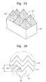
- the light incidence surface 101 includes first protrusions 105.
- the first protrusions 105 have a pyramid shape, and have a triangular shape when viewed in a sectional view.
- the first protrusions 105 may scatter light introduced into the semiconductor substrate 100 from an exterior through the light incidence surface 101 to lengthen an optical path of the light in the semiconductor substrate 100.
- the second optical path L2 of the second light 11 may be longer than the first optical path L1 of the first light 10. This is because the direction of the second optical path L2 of the second light 11 is inclined with respect to the semiconductor substrate 100 due to one of the first protrusions 105 differently from the direction of the first optical path L1 of the first light 10 that is perpendicular to the semiconductor substrate 100.
- a thickness of the semiconductor substrate 100 increases, a short circuit current density of the photovoltaic device 500 may increase, so that the photoelectric conversion efficiency of the photovoltaic device 500 can be improved.
- an optical path is lengthened in the semiconductor substrate 100, optical energy may be more smoothly absorbed into the semiconductor substrate 100, and thus the photoelectric conversion efficiency of the photovoltaic device 500 can be improved.
- Second protrusions 108 are provided on the surface of the first protrusions 105.
- the second protrusions 108 may randomly protrude from the surface of the first protrusions 105.
- the second protrusions 108 have the same function as that of the first protrusions 105.
- the second protrusions 108 may scatter light received introduced into the semiconductor substrate 100 from an exterior through the light incidence surface 101. Accordingly, the light introduced into the semiconductor substrate 100 from an exterior through the light incidence surface 101 can be more dispersed by the second protrusions 108 provided on the surface of the first protrusions 105, so that the photoelectric conversion efficiency of the photovoltaic device 500 can be more improved.
- the semiconductor layer 110 is provided above the semiconductor substrate 100.
- the semiconductor layer 110 includes non-single crystalline silicon such as, for example, amorphous silicon (a-Si) or microcrystalline silicon ( ⁇ c-Si).
- the semiconductor layer 110 is doped with a 3-group element such as, for example, boron (B) to have an electric characteristic of a P-type semiconductor. Accordingly, the semiconductor layer 110 makes P-N junction with the semiconductor substrate 100 having an electric characteristic of an N-type semiconductor.
- an intrinsic non-single crystalline silicon layer having a thin thickness of, for example, about 20 ⁇ to about 100 ⁇ may be interposed between the semiconductor substrate 100 having an N-type semiconductor characteristic and the semiconductor layer 110 having a P-type semiconductor characteristic.
- the structure of a photovoltaic device, in which an intrinsic non-single crystalline silicon layer is interposed between the semiconductor substrate 100 and the semiconductor layer 110, will be described in more detail with reference to FIG. 3 .
- the first electrode 120 is provided on the semiconductor layer 110.
- the first electrode 120 includes a transparent conductive material such as, for example, indium tin oxide (ITO), indium zinc oxide (IZO), zinc oxide (ZnO), or tin oxide (SnO 2 ) such that external light can smoothly reach the semiconductor layer 110 and the semiconductor substrate 100.
- ITO indium tin oxide
- IZO indium zinc oxide
- ZnO zinc oxide
- SnO 2 tin oxide
- the second electrode 130 is provided on a rear surface of the semiconductor substrate 100.
- the second electrode 130 may include metal, such as, for example, aluminum (Al) or silver (Ag), having high reflectance.
- the second electrode 130 may include the same material as that of the first electrode 120. Electrons, which are created from the semiconductor substrate 100 and the semiconductor layer 110 due to photovoltaic effect, may be emitted to an exterior through the first and second electrodes 120 and 130.
- the photovoltaic device 500 may further include an N+ non-single crystalline silicon layer, which is interposed between the semiconductor substrate 100 and the second electrode 130, and an intrinsic non-single crystalline silicon layer, which is interposed between the semiconductor substrate 100 and the N+ non-single crystalline silicon layer.
- the N+ non-single crystalline silicon layer serves as a back surface field (BSF) to improve collection of electrons.
- BSF back surface field
- a photovoltaic device further including the N+ non-single crystalline silicon layer and the intrinsic non-single crystalline silicon layer will be described in more detail with reference to FIG. 3 .
- FIG. 2A is an enlarged view of the first protrusions 105 shown in FIG. 1
- FIG. 2B is an enlarged view of a portion of a sectional surface of the photovoltaic device 500 shown in FIG. 1 .
- the first protrusions 105 have a pyramid shape. This is because the etching rate of the semiconductor substrate 100 including single crystalline silicon is higher in a ⁇ 100> direction than in a ⁇ 111> direction.
- the second protrusions 108 are provided on the surface of the first protrusions 105.
- the size of the first protrusions 105 is greater than that of the second protrusion 108.
- the size of the first protrusions 105 is greater than that of the second protrusions 108.
- a ratio of a first height H1 of the first protrusions 105 to a second height H2 of the second protrusion 108 is in the range of, for example, about 20:1 to about 200:1.
- the first height H1 is in the range of about 2 ⁇ m to about 7 ⁇ m
- the second height H2 is in the range of about 50nm to about 100nm.
- a reflective index of the light is reduced on the light incidence surface 101 due to the first and second protrusions 105 and 108.
- quantity of absorbed light used to induce photovoltaic effect may increase in the semiconductor substrate 100, so that the photoelectric conversion efficiency of the photovoltaic device 500 (see FIG. 1 ) may increase. This will be described in more detail with reference to FIG 7 .
- FIG. 3 is a sectional view showing another exemplary embodiment of a photovoltaic device according to the present invention.
- the same reference numerals denote the same elements in FIG 1 , and thus detailed descriptions of the same elements will be omitted.
- a photovoltaic device 501 further includes a first intrinsic non-single crystalline silicon layer 115, a second intrinsic non-single crystalline silicon layer 116, and a silicon layer 119 including heavily doped impurities, as compared with the photovoltaic device 500 (see FIG. 1 ) according to the previous embodiment of the present invention.
- the first intrinsic non-single crystalline silicon layer 115 includes intrinsic non-single crystalline silicon such as, for example, amorphous silicon (a-Si) or microcrystalline silicon ( ⁇ c-Si), and may have a thickness of, for example, about 20 ⁇ to about 100 ⁇ .
- the first intrinsic non-single crystalline silicon layer 115 is interposed between the semiconductor substrate 100 and the semiconductor layer 110 to increase photoelectric conversion efficiency of the photovoltaic device 501 and to reduce contact resistance between the semiconductor substrate 100 and the semiconductor layer 110.
- the silicon layer 119 including heavily doped impurities is interposed between the second intrinsic non-single crystalline silicon layer 116 and the second electrode 130.
- the silicon layer 119 including heavily doped impurities includes silicon (such as, for example, N+ non-single crystalline silicon) with impurity concentration greater than that of the semiconductor substrate 100, so that electrons created due to photovoltaic effect are more smoothly emitted to an exterior through the second electrode 130.
- the second intrinsic non-single crystalline silicon layer 116 includes intrinsic non-single crystalline silicon such as, for example, amorphous silicon (a-Si) or microcrystalline silicon ( ⁇ c-Si).
- the second intrinsic non-single crystalline silicon layer 116 is formed on a rear surface 104 of the semiconductor substrate 100 to reduce contact resistance between the semiconductor substrate 100 and the silicon layer 119 including heavily doped impurities.
- third protrusions 106 are provided on the rear surface 104, and fourth protrusions 109 are provided on the surface of the third protrusions 106.
- the third protrusions 106 may have the same shape as that of the first protrusions 105, and the fourth protrusions 109 may have the same shape as that of the second protrusions 108.
- the third and fourth protrusions 106 and 109 increase an optical path in the semiconductor substrate 100 to raise photoelectric conversion efficiency of the photovoltaic device 501.
- the second electrode 130 includes a material (e.g., aluminum (Al) or silver (Ag)) reflecting light according to the present exemplary embodiments
- a material e.g., aluminum (Al) or silver (Ag) reflecting light
- light which is incident through the light incidence surface 101, but not absorbed in the semiconductor substrate 100, is reflected on the second electrode 130.
- the light reflected on the second electrode 130 is again scattered by the third and fourth protrusions 106 and 109 Accordingly, an optical path of the light may be increased in the semiconductor substrate 100, so that photoelectric conversion efficiency of the photovoltaic device 501 can be improved.
- FIGS. 4A and 5A are sectional views illustrating an exemplary embodiment of a method of manufacturing the photovoltaic device 501 shown in FIG. 3
- FIGS. 4B and 5B are photographs showing the light incidence surface 101 of the semiconductor substrate 100 in the manufacturing step of the photovoltaic device 501 of FIGS. 4A and 5A
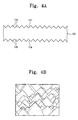
- FIG. 4A is a sectional view showing a process of wet-etching the semiconductor substrate 100
- FIG. 4B is a photograph showing the light incidence surface 101 of the semiconductor substrate 100 after the semiconductor substrate 100 is wet-etched
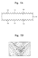
- FIG. 5A is a sectional view showing a process of dry-etching the semiconductor substrate 100
- FIG. 5B is a photograph showing the light incidence surface 101 of the semiconductor substrate 100 after the semiconductor substrate 100 is dry-etched.
- the semiconductor substrate 100 having the light incidence surface 101 is wet-etched, so that the first protrusions 105 are formed on the light incidence surface 101.
- the semiconductor substrate 100 is immersed into a vessel receiving etchant solution such that the semiconductor substrate 100 is etched.
- the light incidence surface 101 and the rear surface 104 of the semiconductor substrate 100 facing the light incidence surface 101 are etched by the etchant solution.
- the third protrusions 106 having the same shape as that of the first protrusions 105 are formed on the rear surface 104.
- the etchant solution used to wet-etch the semiconductor substrate 100 may include, for example, an alkaline solution.
- the etchant solution may include, for example, potassium hydroxide (KOH) and isopropyl alcohol (IPA).
- KOH potassium hydroxide
- IPA isopropyl alcohol
- the etchant solution includes potassium hydroxide (KOH)
- KOH potassium hydroxide
- NaOH sodium hydroxide
- the first protrusions 105 which are formed by etching the light incidence surface 101, can have a more uniform size.
- the etchant solution includes the potassium hydroxide (KOH)
- KOH potassium hydroxide
- the potassium ions (K+) are less bonded with electrons when compared to other ions (e.g., sodium ions (Na+)).
- the etchant solution includes potassium hydroxide (KOH)
- positive ions generated from the etchant solution are bonded with electrons created due to the photovoltaic effect, so that the reduction of quantity of current in the photovoltaic device 501 can be minimized.
- the semiconductor substrate 100 is etched by immersing the semiconductor substrate 100 into etchant solution to form the first protrusions 105
- the semiconductor substrate 100 may be etched by spraying the etchant solution to the semiconductor substrate 100.
- the semiconductor substrate 100 including the first and third protrusions 105 and 106 is dry-etched. Accordingly, the second protrusions 108 are formed on the surface of the first protrusions 105, and the fourth protrusions 109 are formed on the surface of the third protrusions 106.
- the dry-etching is performed by using, for example, a gas mixture of first gas including fluorine (F) and second gas including chlorine (Cl).
- the first gas may include, for example, sulfur hexafluoride (SF 6 )
- the second gas may include, for example, chlorine gas (Cl 2 ).
- the flow rate ratio of the first gas and the second gas is, for example, about 1: 1 to about 3:1.
- the flow rate ratio of the first gas and the second gas is, for example, about 1: 1. The reason to employ the flow rate ratio of about 1:1 will be described with reference to FIGS. 6A to 6C .
- edges of the first protrusions 105 are rounded by the second protrusions 108 as shown in FIG. 5B . Accordingly, if the second protrusions 108 are formed on the first protrusions 105, thin films formed on the first protrusions 105 are prevented from being cut by sharp edges of inclined surfaces defining the first protrusions 105 in a region at which the inclined surfaces meet each other.
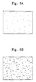
- FIGS. 6A to 6C are photographs showing the light incidence surface 101 (see FIG. 5A ) of the semiconductor substrate 100 according to types of etchant gas used for the dry-etching.
- FIG. 6A is a photograph showing a state of the light incidence surface 101 after etching the light incidence surface 101 by applying, for example, chlorine gas (Cl 2 ) into a plasma dry etching device, which is supplied with RF power of about 2000W under an internal pressure of about 100mT, at a flow rate of about 200 sccm, in which "sccm" represents standard cubic centimeters per minute.
- Cl 2 chlorine gas
- FIG. 6B is a photograph showing a state of the light incidence surface 101 after etching the light incidence surface 101 by applying, for example, sulfur hexafluoride (SF 6 ) into the plasma dry etching device, which is supplied with RF power of about 2000W under an internal pressure of about 100mT, at a flow rate of 200 sccm.
- FIG. 6C is a photograph showing a state of the light incidence surface 101 after etching the light incidence surface 101 by applying, for example, chlorine gas (Cl 2 ) and sulfur hexafluoride (SF 6 ) into the plasma dry etching device, which is supplied with RF power of about 2000W under an internal pressure of about 100mT, at a flow rate of about 200 sccm.
- SF 6 sulfur hexafluoride
- the second protrusions 108 are rarely formed on the light incidence surface 101 of the semiconductor substrate 100.
- the second protrusions 108 are formed on the light incidence surface 101.
- the number of the second protrusions 108 per unit area shown in FIG. 6C is greater than the number of the second protrusions 108 per unit area shown in FIG. 6B .
- the semiconductor substrate 100 is dry-etched by using, for example, gas obtained by mixing chlorine gas (Cl 2 ) and sulfur hexafluoride (SF 6 ) at the same flow rate, the texturing effect for the light incidence surface 101 may be maximized.
- Cl 2 chlorine gas
- SF 6 sulfur hexafluoride
- the dry-etching is preferably performed for, example, about 15 seconds to about 120 seconds, in more detail, about 30 seconds. This is because the semiconductor substrate 100 should be subjected to the dry-etching process for at least 15 seconds by taking stabilization time of plasma into consideration.
- the semiconductor substrate 100 when the semiconductor substrate 100 is dry-etched for more than about 120 seconds, even if light absorbance of the semiconductor substrate 100 increases with respect to light having a wavelength of about 1000nm or more, the light absorbance of the semiconductor substrate 100 may be reduced with respect to light having a wavelength of about 400nm to about 1000nm, so that the light absorbance is rarely increased over the whole wavelength band of light.
- an oxide layer which is formed on the semiconductor substrate 100 after the first and third protrusions 105 and 106 are formed, is removed from the surface of the semiconductor substrate 100.
- the oxide layer may include, for example, silicon oxide (SiOx) formed by combining external oxygen (O) with silicon (Si) of the semiconductor substrate 100.
- the oxide layer may be etched by using, for example, boron trichloride (BCl 3 ) or a gas mixture of boron trichloride (BCl 3 ) and chlorine gas (Cl 2 ).
- the first intrinsic non-single crystalline silicon layer 115 is formed on the light incidence surface 101 of the semiconductor substrate 100, the semiconductor layer 110 having a P-type semiconductor characteristic is formed on the first intrinsic non-single crystalline silicon layer 115, and the first electrode 120 is formed on the semiconductor layer 110.
- the second intrinsic non-single crystalline silicon layer 116 is formed on the rear surface 104 of the semiconductor substrate 100, the silicon layer 119 including heavily doped impurities is formed on the second intrinsic non-single crystalline silicon layer 116, and the second electrode 130 is formed on the silicon layer 119 including heavily doped impurities, thereby manufacturing the photovoltaic device 501.
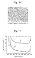
- FIG. 7 shows first to third curves G1, G2, and G3 representing reflective indexes of the semiconductor substrate 100.
- FIG. 7 shows the first to third curves G1, G2, and G3 showing the reflective indexes of the semiconductor substrate 100 obtained from experiment according to three states of the light incidence surface 101 of the semiconductor substrate 100.
- the reflective indexes of the semiconductor substrate 100 (see FIG. 1 ) according to wavelengths of light are classified according to three states of the light incidence surface 101 (see FIG. 1 ) of the semiconductor substrate 100 (see FIG. 1 ).
- the three states are classified into first to third surface states.
- the first to third curves G1 to G3 represent reflective indexes of the semiconductor substrate 100 having the first to third surface states, respectively.
- the first surface state represents a flat surface of the light incidence surface 101 when the light incidence surface 101 is not subject to any etching processes.
- the second surface state represents a state of the light incidence surface 101 when the light incidence surface 101 is wet-etched to form the first protrusions 105 (see FIG. 4A ) on the light incidence surface 101.
- the third surface state represents a state of the light incidence surface 101 when the light incidence surface 101 is wet-etched and dry-etched, so that the first protrusions 105 are formed on the light incidence surface 101, and the second protrusions 108 (see FIG. 5B ) are formed on the surface of the first protrusions 105.
- the reflective index of the semiconductor substrate 100 having the second surface state is lower than the reflective index of the semiconductor substrate 100 having the first surface state over the whole wavelength region of light.
- the reflective index of the semiconductor substrate 100 having the third surface state is lower than the reflective index of the semiconductor substrate 100 having the second surface state over the whole wavelength region of the light.
- the reflective index of the semiconductor substrate 100 having the third surface state is significantly lower than the reflective index of the semiconductor substrate 100 having the second surface state.
- the semiconductor substrate 100 can absorb much more of the light in a specific wavelength band.
Landscapes
- Photovoltaic Devices (AREA)
Abstract
Description
- This application relies for priority upon Korean Patent Application No.
2008-75261 filed on July 31, 2008 - The present disclosure relates to a method of manufacturing a photovoltaic device. More particularly, the present disclosure relates to a method of manufacturing a photovoltaic device capable of improving photoelectric conversion efficiency.
- A photovoltaic device may convert optical energy into electric energy. Generally, the photovoltaic device includes a semiconductor layer which may induce photovoltaic effect by absorbing external optical energy, and first and second electrodes between which the semiconductor layer is interposed.
- Meanwhile, photoelectric conversion efficiency of the photovoltaic device may be determined by characteristics such as, for example, open circuit voltage, a fill factor, and a short circuit current density. Among them, the short circuit current density may increase by increasing light absorbing efficiency representing quantity of current generated from the photovoltaic device in relation to quantity of light supplied from an exterior to the semiconductor layer. Although the photoelectric conversion efficiency of the photovoltaic device may increase by enlarging the thickness of the semiconductor layer to lengthen a path of light traveling in the semiconductor layer, the manufacturing costs and manufacturing time of the photovoltaic device may increase if the thickness of the semiconductor layer increases. In addition, as the characteristic of the fill factor may degraded, improvement in the photoelectric conversion efficiency may be difficult to obtain.
- An exemplary embodiment of the present invention may provide a method of manufacturing a photovoltaic device capable of improving photoelectric conversion efficiency.
- In accordance with an exemplary embodiment of the present invention, a method of manufacturing a photovoltaic device is provided. The method includes preparing a semiconductor substrate having a light incidence surface receiving light and including single crystalline silicon, wet-etching the light incidence surface to form a plurality of first protrusions on the light incidence surface, dry etching a plurality of surfaces of the plurality of first protrusions to form a plurality of second protrusions on the plurality of surfaces of the first protrusion, and forming a semiconductor layer on the light incidence surface. The method further includes forming a first electrode on the semiconductor layer and forming a second electrode on a rear surface of the semiconductor substrate facing the light incidence surface.
- Accordingly, a light introduced into the semiconductor substrate from an exterior through the light incidence surface may be scattered on the light incidence surface by the plurality of first and second protrusions, so that an optical path of the light is lengthened in the semiconductor substrate, thereby improving photoelectric conversion efficiency. As a result, as optical energy is more smoothly absorbed into the semiconductor substrate, the photoelectric conversion efficiency of the photovoltaic device can be improved.
- Exemplary embodiments of the present invention can be understood in more detail from the following description when considered in conjunction with the accompanying drawings wherein:
-
FIG. 1 is a sectional view showing an exemplary embodiment of a photovoltaic device according to an exemplary embodiment of the present invention; -
FIG. 2A is an enlarged view of first protrusions shown inFIG. 1 ; -
FIG. 2B is an enlarged view of a portion of a sectional surface of the photovoltaic device shown inFIG. 1 ; -
FIG. 3 is a sectional view showing an exemplary embodiment of a photovoltaic device according to the present invention; -
FIGS. 4A and5A are sectional views illustrating an exemplary embodiment of a method of manufacturing the photovoltaic device shown inFIG. 3 ; -
FIG. 4B is a photograph showing a light incidence surface of a semiconductor substrate in the manufacturing step of the photovoltaic device shown inFIG. 4A ; -
FIG. 5B is a photograph showing a light incidence surface of a semiconductor substrate in the manufacturing step of the photovoltaic device shown inFIG. 5A ; -
FIGS. 6A to 6C are photographs showing a light incidence surface of a semiconductor substrate according to types of etchant gas used for a dry-etching process; and -
FIG. 7 is a graph representing reflective indexes of a semiconductor substrate. - Hereinafter, exemplary embodiments of the present invention will be described in detail with reference to accompanying drawings. It is understood that the present invention should not be limited to the following exemplary embodiments but various changes and modifications can be made by one ordinary skilled in the art within the spirit and scope of the present invention. The present invention is defined only by the scope of the appended claims. Meanwhile, elements shown in the drawings can be simplified or magnified for the purpose of clear explanation. In addition, the same reference numerals are used to designate the same elements throughout the drawings.
-
FIG. 1 is a sectional view showing an exemplary embodiment of a photovoltaic device according to the present invention. - Referring to
FIG. 1 , aphotovoltaic device 500 includes asemiconductor substrate 100, asemiconductor layer 110, afirst electrode 120, and asecond electrode 130. - The
semiconductor substrate 100 includes single crystalline silicon, and is formed by doping a 5-group element such as, for example, phosphorus (P) into a silicon wafer, so that thesemiconductor substrate 100 has an electric characteristic of an N-type semiconductor. In addition, thesemiconductor substrate 100 has alight incidence surface 101 receiving light from an exterior. When thesemiconductor substrate 100 receives light from an exterior through thelight incidence surface 101, photovoltaic effect may be induced. Through the photovoltaic effect, electrons are created in thesemiconductor substrate 100, and emitted to an exterior through thefirst electrode 120 or thesecond electrode 130. - The
light incidence surface 101 includesfirst protrusions 105. Thefirst protrusions 105 have a pyramid shape, and have a triangular shape when viewed in a sectional view. Thefirst protrusions 105 may scatter light introduced into thesemiconductor substrate 100 from an exterior through thelight incidence surface 101 to lengthen an optical path of the light in thesemiconductor substrate 100. - For example, when a
first light 10 and asecond light 11 reach thelight incidence surface 101 from an exterior perpendicularly to thesemiconductor substrate 100, if the direction of a first optical path L1 of afirst light 10 is not changed on thelight incidence surface 101, but the direction of a second optical path L2 of asecond light 11 is changed on thelight incidence surface 101, the second optical path L2 of thesecond light 11 may be longer than the first optical path L1 of thefirst light 10. This is because the direction of the second optical path L2 of thesecond light 11 is inclined with respect to thesemiconductor substrate 100 due to one of thefirst protrusions 105 differently from the direction of the first optical path L1 of thefirst light 10 that is perpendicular to thesemiconductor substrate 100. - If a thickness of the
semiconductor substrate 100 increases, a short circuit current density of thephotovoltaic device 500 may increase, so that the photoelectric conversion efficiency of thephotovoltaic device 500 can be improved. Similarly, if an optical path is lengthened in thesemiconductor substrate 100, optical energy may be more smoothly absorbed into thesemiconductor substrate 100, and thus the photoelectric conversion efficiency of thephotovoltaic device 500 can be improved. -
Second protrusions 108 are provided on the surface of thefirst protrusions 105. Thesecond protrusions 108 may randomly protrude from the surface of thefirst protrusions 105. Thesecond protrusions 108 have the same function as that of thefirst protrusions 105. In other words, thesecond protrusions 108 may scatter light received introduced into thesemiconductor substrate 100 from an exterior through thelight incidence surface 101. Accordingly, the light introduced into thesemiconductor substrate 100 from an exterior through thelight incidence surface 101 can be more dispersed by thesecond protrusions 108 provided on the surface of thefirst protrusions 105, so that the photoelectric conversion efficiency of thephotovoltaic device 500 can be more improved. - The
semiconductor layer 110 is provided above thesemiconductor substrate 100. Thesemiconductor layer 110 includes non-single crystalline silicon such as, for example, amorphous silicon (a-Si) or microcrystalline silicon (µ c-Si). In addition, thesemiconductor layer 110 is doped with a 3-group element such as, for example, boron (B) to have an electric characteristic of a P-type semiconductor. Accordingly, thesemiconductor layer 110 makes P-N junction with thesemiconductor substrate 100 having an electric characteristic of an N-type semiconductor. In addition, to increase photoelectric conversion efficiency, an intrinsic non-single crystalline silicon layer having a thin thickness of, for example, about 20Å to about 100Å may be interposed between thesemiconductor substrate 100 having an N-type semiconductor characteristic and thesemiconductor layer 110 having a P-type semiconductor characteristic. The structure of a photovoltaic device, in which an intrinsic non-single crystalline silicon layer is interposed between thesemiconductor substrate 100 and thesemiconductor layer 110, will be described in more detail with reference toFIG. 3 . - The
first electrode 120 is provided on thesemiconductor layer 110. Thefirst electrode 120 includes a transparent conductive material such as, for example, indium tin oxide (ITO), indium zinc oxide (IZO), zinc oxide (ZnO), or tin oxide (SnO2) such that external light can smoothly reach thesemiconductor layer 110 and thesemiconductor substrate 100. - The
second electrode 130 is provided on a rear surface of thesemiconductor substrate 100. Thesecond electrode 130 may include metal, such as, for example, aluminum (Al) or silver (Ag), having high reflectance. Thesecond electrode 130 may include the same material as that of thefirst electrode 120. Electrons, which are created from thesemiconductor substrate 100 and thesemiconductor layer 110 due to photovoltaic effect, may be emitted to an exterior through the first andsecond electrodes - Meanwhile, the
photovoltaic device 500 may further include an N+ non-single crystalline silicon layer, which is interposed between thesemiconductor substrate 100 and thesecond electrode 130, and an intrinsic non-single crystalline silicon layer, which is interposed between thesemiconductor substrate 100 and the N+ non-single crystalline silicon layer. The N+ non-single crystalline silicon layer serves as a back surface field (BSF) to improve collection of electrons. A photovoltaic device further including the N+ non-single crystalline silicon layer and the intrinsic non-single crystalline silicon layer will be described in more detail with reference toFIG. 3 . -
FIG. 2A is an enlarged view of thefirst protrusions 105 shown inFIG. 1 , andFIG. 2B is an enlarged view of a portion of a sectional surface of thephotovoltaic device 500 shown inFIG. 1 . - Referring to
FIGS. 2A and 2B , thefirst protrusions 105 have a pyramid shape. This is because the etching rate of thesemiconductor substrate 100 including single crystalline silicon is higher in a <100> direction than in a <111> direction. - The
second protrusions 108 are provided on the surface of thefirst protrusions 105. The size of thefirst protrusions 105 is greater than that of thesecond protrusion 108. For example , when comparing the size of thefirst protrusions 105 with the size of thesecond protrusions 108 by using parameters (e.g., height, width, and length) capable of determining the size of a protrusion in general, the size of thefirst protrusions 105 is greater than that of thesecond protrusions 108. - A ratio of a first height H1 of the
first protrusions 105 to a second height H2 of thesecond protrusion 108 is in the range of, for example, about 20:1 to about 200:1. For example, the first height H1 is in the range of about 2µm to about 7µm, and the second height H2 is in the range of about 50nm to about 100nm. - Meanwhile, when light is supplied to the
semiconductor substrate 100 through thelight incidence surface 101, a reflective index of the light is reduced on thelight incidence surface 101 due to the first andsecond protrusions light incidence surface 101, quantity of absorbed light used to induce photovoltaic effect may increase in thesemiconductor substrate 100, so that the photoelectric conversion efficiency of the photovoltaic device 500 (seeFIG. 1 ) may increase. This will be described in more detail with reference toFIG 7 . -
FIG. 3 is a sectional view showing another exemplary embodiment of a photovoltaic device according to the present invention. InFIG. 3 , the same reference numerals denote the same elements inFIG 1 , and thus detailed descriptions of the same elements will be omitted. - Referring to
FIG. 3 , aphotovoltaic device 501 further includes a first intrinsic non-singlecrystalline silicon layer 115, a second intrinsic non-singlecrystalline silicon layer 116, and asilicon layer 119 including heavily doped impurities, as compared with the photovoltaic device 500 (seeFIG. 1 ) according to the previous embodiment of the present invention. - The first intrinsic non-single
crystalline silicon layer 115 includes intrinsic non-single crystalline silicon such as, for example, amorphous silicon (a-Si) or microcrystalline silicon (µ c-Si), and may have a thickness of, for example, about 20Å to about 100Å. The first intrinsic non-singlecrystalline silicon layer 115 is interposed between thesemiconductor substrate 100 and thesemiconductor layer 110 to increase photoelectric conversion efficiency of thephotovoltaic device 501 and to reduce contact resistance between thesemiconductor substrate 100 and thesemiconductor layer 110. - The
silicon layer 119 including heavily doped impurities is interposed between the second intrinsic non-singlecrystalline silicon layer 116 and thesecond electrode 130. When thesemiconductor substrate 100 and thesemiconductor layer 110 have N-type and P-type semiconductor characteristics, respectively, thesilicon layer 119 including heavily doped impurities includes silicon (such as, for example, N+ non-single crystalline silicon) with impurity concentration greater than that of thesemiconductor substrate 100, so that electrons created due to photovoltaic effect are more smoothly emitted to an exterior through thesecond electrode 130. - The second intrinsic non-single
crystalline silicon layer 116 includes intrinsic non-single crystalline silicon such as, for example, amorphous silicon (a-Si) or microcrystalline silicon (µ c-Si). The second intrinsic non-singlecrystalline silicon layer 116 is formed on arear surface 104 of thesemiconductor substrate 100 to reduce contact resistance between thesemiconductor substrate 100 and thesilicon layer 119 including heavily doped impurities. - Meanwhile,
third protrusions 106 are provided on therear surface 104, andfourth protrusions 109 are provided on the surface of thethird protrusions 106. Thethird protrusions 106 may have the same shape as that of thefirst protrusions 105, and thefourth protrusions 109 may have the same shape as that of thesecond protrusions 108. In addition, similarly to the first andsecond protrusions fourth protrusions semiconductor substrate 100 to raise photoelectric conversion efficiency of thephotovoltaic device 501. - For example , when the
second electrode 130 includes a material (e.g., aluminum (Al) or silver (Ag)) reflecting light according to the present exemplary embodiments, light, which is incident through thelight incidence surface 101, but not absorbed in thesemiconductor substrate 100, is reflected on thesecond electrode 130. The light reflected on thesecond electrode 130 is again scattered by the third andfourth protrusions semiconductor substrate 100, so that photoelectric conversion efficiency of thephotovoltaic device 501 can be improved. -
FIGS. 4A and5A are sectional views illustrating an exemplary embodiment of a method of manufacturing thephotovoltaic device 501 shown inFIG. 3 , andFIGS. 4B and5B are photographs showing thelight incidence surface 101 of thesemiconductor substrate 100 in the manufacturing step of thephotovoltaic device 501 ofFIGS. 4A and5A . For example ,FIG. 4A is a sectional view showing a process of wet-etching thesemiconductor substrate 100, andFIG. 4B is a photograph showing thelight incidence surface 101 of thesemiconductor substrate 100 after thesemiconductor substrate 100 is wet-etched. In addition,FIG. 5A is a sectional view showing a process of dry-etching thesemiconductor substrate 100, andFIG. 5B is a photograph showing thelight incidence surface 101 of thesemiconductor substrate 100 after thesemiconductor substrate 100 is dry-etched. - Referring to
FIGS. 4A and 4B , thesemiconductor substrate 100 having thelight incidence surface 101 is wet-etched, so that thefirst protrusions 105 are formed on thelight incidence surface 101. In the present exemplary embodiment, thesemiconductor substrate 100 is immersed into a vessel receiving etchant solution such that thesemiconductor substrate 100 is etched. As a result, thelight incidence surface 101 and therear surface 104 of thesemiconductor substrate 100 facing thelight incidence surface 101 are etched by the etchant solution. Accordingly, thethird protrusions 106 having the same shape as that of thefirst protrusions 105 are formed on therear surface 104. - The etchant solution used to wet-etch the
semiconductor substrate 100 may include, for example, an alkaline solution. In more detail, the etchant solution may include, for example, potassium hydroxide (KOH) and isopropyl alcohol (IPA). When the etchant solution includes potassium hydroxide (KOH), as the potassium hydroxide (KOH) provides an etching rate for thesemiconductor substrate 100 slower than an etching rate provided by another etchant solution (e.g., sodium hydroxide (NaOH)), thefirst protrusions 105, which are formed by etching thelight incidence surface 101, can have a more uniform size. In addition, when the etchant solution includes the potassium hydroxide (KOH), even if potassium ions (K+) remain on the surface of thesemiconductor substrate 100 after thesemiconductor substrate 100 is wet-etched, the potassium ions (K+) are less bonded with electrons when compared to other ions (e.g., sodium ions (Na+)). Accordingly, if the etchant solution includes potassium hydroxide (KOH), positive ions generated from the etchant solution are bonded with electrons created due to the photovoltaic effect, so that the reduction of quantity of current in thephotovoltaic device 501 can be minimized. - Meanwhile, according to the present exemplary embodiment, although the
semiconductor substrate 100 is etched by immersing thesemiconductor substrate 100 into etchant solution to form thefirst protrusions 105, thesemiconductor substrate 100 may be etched by spraying the etchant solution to thesemiconductor substrate 100. - Referring to
FIGS. 5A and 5B , thesemiconductor substrate 100 including the first andthird protrusions second protrusions 108 are formed on the surface of thefirst protrusions 105, and thefourth protrusions 109 are formed on the surface of thethird protrusions 106. - The dry-etching is performed by using, for example, a gas mixture of first gas including fluorine (F) and second gas including chlorine (Cl). In more detail, the first gas may include, for example, sulfur hexafluoride (SF6), and the second gas may include, for example, chlorine gas (Cl2). In the mixed gas, the flow rate ratio of the first gas and the second gas is, for example, about 1: 1 to about 3:1. In more detail, preferably, the flow rate ratio of the first gas and the second gas is, for example, about 1: 1. The reason to employ the flow rate ratio of about 1:1 will be described with reference to
FIGS. 6A to 6C . - Meanwhile, when the
second protrusions 108 are formed by dry-etching thesemiconductor substrate 100, edges of thefirst protrusions 105 are rounded by thesecond protrusions 108 as shown inFIG. 5B . Accordingly, if thesecond protrusions 108 are formed on thefirst protrusions 105, thin films formed on thefirst protrusions 105 are prevented from being cut by sharp edges of inclined surfaces defining thefirst protrusions 105 in a region at which the inclined surfaces meet each other. -
FIGS. 6A to 6C are photographs showing the light incidence surface 101 (seeFIG. 5A ) of thesemiconductor substrate 100 according to types of etchant gas used for the dry-etching. In more detail,FIG. 6A is a photograph showing a state of thelight incidence surface 101 after etching thelight incidence surface 101 by applying, for example, chlorine gas (Cl2) into a plasma dry etching device, which is supplied with RF power of about 2000W under an internal pressure of about 100mT, at a flow rate of about 200 sccm, in which "sccm" represents standard cubic centimeters per minute.FIG. 6B is a photograph showing a state of thelight incidence surface 101 after etching thelight incidence surface 101 by applying, for example, sulfur hexafluoride (SF6) into the plasma dry etching device, which is supplied with RF power of about 2000W under an internal pressure of about 100mT, at a flow rate of 200 sccm.FIG. 6C is a photograph showing a state of thelight incidence surface 101 after etching thelight incidence surface 101 by applying, for example, chlorine gas (Cl2) and sulfur hexafluoride (SF6) into the plasma dry etching device, which is supplied with RF power of about 2000W under an internal pressure of about 100mT, at a flow rate of about 200 sccm. - Referring to
FIG. 6A , when thesemiconductor substrate 100 is dry-etched by using, for example, only chlorine gas (Cl2), thesecond protrusions 108 are rarely formed on thelight incidence surface 101 of thesemiconductor substrate 100. Referring toFIGS. 6B and6C , thesecond protrusions 108 are formed on thelight incidence surface 101. However, the number of thesecond protrusions 108 per unit area shown inFIG. 6C is greater than the number of thesecond protrusions 108 per unit area shown inFIG. 6B . In other words, when thesemiconductor substrate 100 is dry-etched by using, for example, gas obtained by mixing chlorine gas (Cl2) and sulfur hexafluoride (SF6) at the same flow rate, the texturing effect for thelight incidence surface 101 may be maximized. - Referring again to
FIGS. 5A and 5B , when thesemiconductor substrate 100 is dry-etched to form the second andfourth protrusions semiconductor substrate 100 should be subjected to the dry-etching process for at least 15 seconds by taking stabilization time of plasma into consideration. In addition, when thesemiconductor substrate 100 is dry-etched for more than about 120 seconds, even if light absorbance of thesemiconductor substrate 100 increases with respect to light having a wavelength of about 1000nm or more, the light absorbance of thesemiconductor substrate 100 may be reduced with respect to light having a wavelength of about 400nm to about 1000nm, so that the light absorbance is rarely increased over the whole wavelength band of light. - Meanwhile, before the second and
fourth protrusions semiconductor substrate 100, an oxide layer, which is formed on thesemiconductor substrate 100 after the first andthird protrusions semiconductor substrate 100. The oxide layer may include, for example, silicon oxide (SiOx) formed by combining external oxygen (O) with silicon (Si) of thesemiconductor substrate 100. The oxide layer may be etched by using, for example, boron trichloride (BCl3) or a gas mixture of boron trichloride (BCl3) and chlorine gas (Cl2). - Referring again to
FIG. 3 , the first intrinsic non-singlecrystalline silicon layer 115 is formed on thelight incidence surface 101 of thesemiconductor substrate 100, thesemiconductor layer 110 having a P-type semiconductor characteristic is formed on the first intrinsic non-singlecrystalline silicon layer 115, and thefirst electrode 120 is formed on thesemiconductor layer 110. In addition, the second intrinsic non-singlecrystalline silicon layer 116 is formed on therear surface 104 of thesemiconductor substrate 100, thesilicon layer 119 including heavily doped impurities is formed on the second intrinsic non-singlecrystalline silicon layer 116, and thesecond electrode 130 is formed on thesilicon layer 119 including heavily doped impurities, thereby manufacturing thephotovoltaic device 501. -
FIG. 7 shows first to third curves G1, G2, and G3 representing reflective indexes of thesemiconductor substrate 100. In more detail,FIG. 7 shows the first to third curves G1, G2, and G3 showing the reflective indexes of thesemiconductor substrate 100 obtained from experiment according to three states of thelight incidence surface 101 of thesemiconductor substrate 100. - Referring to
FIG. 7 , the reflective indexes of the semiconductor substrate 100 (seeFIG. 1 ) according to wavelengths of light are classified according to three states of the light incidence surface 101 (seeFIG. 1 ) of the semiconductor substrate 100 (seeFIG. 1 ). For the convenience of the explanation, the three states are classified into first to third surface states. The first to third curves G1 to G3 represent reflective indexes of thesemiconductor substrate 100 having the first to third surface states, respectively. - The first surface state represents a flat surface of the
light incidence surface 101 when thelight incidence surface 101 is not subject to any etching processes. The second surface state represents a state of thelight incidence surface 101 when thelight incidence surface 101 is wet-etched to form the first protrusions 105 (seeFIG. 4A ) on thelight incidence surface 101. The third surface state represents a state of thelight incidence surface 101 when thelight incidence surface 101 is wet-etched and dry-etched, so that thefirst protrusions 105 are formed on thelight incidence surface 101, and the second protrusions 108 (seeFIG. 5B ) are formed on the surface of thefirst protrusions 105. - Referring to the first to third curves G1 to G3, the reflective index of the
semiconductor substrate 100 having the second surface state is lower than the reflective index of thesemiconductor substrate 100 having the first surface state over the whole wavelength region of light. In addition, the reflective index of thesemiconductor substrate 100 having the third surface state is lower than the reflective index of thesemiconductor substrate 100 having the second surface state over the whole wavelength region of the light. In particular, regarding light having wavelengths in the range of about 250nm to about 400nm and the range of about 900nm to about 1100nm, the reflective index of thesemiconductor substrate 100 having the third surface state is significantly lower than the reflective index of thesemiconductor substrate 100 having the second surface state. In other words, when the second protrusions 108 (seeFIG. 5B ) are additionally formed by dry-etching thesemiconductor substrate 100 after the first protrusions 105 (seeFIG. 4 ) are formed by wet-etching thesemiconductor substrate 100, thesemiconductor substrate 100 can absorb much more of the light in a specific wavelength band. - Having described the exemplary embodiments of the present invention, it is further noted that it is readily apparent to those of reasonable skill in the art that various modifications may be made without departing from the spirit and scope of the invention which is defined by the metes and bounds of the appended claims.
Claims (14)
- A method of manufacturing a photovoltaic device, the method comprising:preparing a semiconductor substrate having a light incidence surface receiving a light, and including single crystalline silicon;wet-etching the light incidence surface to form a plurality of first protrusions on the light incidence surface;dry-etching a plurality of surfaces of the plurality of first protrusions to form a plurality of second protrusions on the plurality of surfaces of the plurality of first protrusions;forming a semiconductor layer on the light incidence surface;forming a first electrode on the semiconductor layer; andforming a second electrode on a rear surface of the semiconductor substrate facing the light incidence surface.
- The method of claim 1, wherein a height ratio of the plurality of first protrusions to the plurality of second protrusions is in a range of about 20:1 1 to about 200:1.
- The method of claim 2, wherein a height of the plurality of first protrusions is in a range of about 2µm to about 7µm.
- The method of claim 3, wherein a height of the plurality of second protrusions are in a range of about 50nm to about 100nm.
- The method of claim 1, wherein an etchant used for the wet-etching comprises potassium hydroxide (KOH).
- The method of claim 1, further comprising:forming a plurality of third protrusions on a rear surface of the semiconductor substrate , wherein the plurality of third protrusions have a same shape as a shape of the plurality of first protrusions; anddry-etching the surfaces of the plurality of third protrusions to form a plurality of fourth protrusions on the plurality of surfaces of the plurality of third protrusions,wherein the plurality of third protrusions are formed together with the plurality of first protrusions.
- The method of claim 1, wherein an etchant used for the dry-etching comprises a gas mixture of a first gas comprising fluorine (F) and a second gas comprising chlorine (Cl).
- The method of claim 7, wherein the first gas comprises sulfur hexafluoride (SF6), and the second gas comprises chlorine (Cl).
- The method of claim 8, wherein a flow rate ratio of the first gas to the second gas is in a range of about 1: 1 to about 3:1.
- The method of claim 9, wherein the dry-etching is performed for about 15 seconds to 120 seconds.
- The method of claim 1, wherein the semiconductor layer comprises non-single crystalline silicon, and is formed through a chemical vapor deposition scheme.
- The method of claim 1, wherein the semiconductor substrate is an N-type semiconductor, and the semiconductor layer is a P-type semiconductor.
- The method of claim 1, further comprising:forming a first intrinsic non-single crystalline silicon layer between the semiconductor substrate and the semiconductor layer;forming a second intrinsic non-single crystalline silicon layer between the semiconductor substrate and the second electrode; andforming a silicon layer comprising heavily doped impurities between the second intrinsic non-single crystalline silicon layer and the second electrode, the silicon layer having an impurity concentration greater than an impurity concentration of the semiconductor substrate.
- The method of claim 1, further comprising removing an oxide layer formed on the semiconductor substrate by using an etchant comprising one of boron trichloride (BCl3) or a gas mixture of boron trichloride (BCl3) and chlorine gas (Cl2), before the dry-etching is performed.
Applications Claiming Priority (1)
| Application Number | Priority Date | Filing Date | Title |
|---|---|---|---|
| KR1020080075261A KR20100013649A (en) | 2008-07-31 | 2008-07-31 | Photovoltaic device and method of manufacturing the same |
Publications (2)
| Publication Number | Publication Date |
|---|---|
| EP2149915A2 true EP2149915A2 (en) | 2010-02-03 |
| EP2149915A3 EP2149915A3 (en) | 2012-10-31 |
Family
ID=41376309
Family Applications (1)
| Application Number | Title | Priority Date | Filing Date |
|---|---|---|---|
| EP09004691A Withdrawn EP2149915A3 (en) | 2008-07-31 | 2009-03-31 | Method of manufacturing photovoltaic device |
Country Status (4)
| Country | Link |
|---|---|
| US (1) | US20100024871A1 (en) |
| EP (1) | EP2149915A3 (en) |
| JP (1) | JP2010041032A (en) |
| KR (1) | KR20100013649A (en) |
Cited By (6)
| Publication number | Priority date | Publication date | Assignee | Title |
|---|---|---|---|---|
| EP2429003A1 (en) * | 2010-09-10 | 2012-03-14 | Byung-Jun Kim | Surface processing method of silicon substrate for solar cell, and method for manufacturing solar cell |
| EP2439791A1 (en) * | 2010-10-08 | 2012-04-11 | Byung-Jun Kim | Method for manufacturing solar cell and solar cell manufactured by the same method |
| EP2645421A1 (en) * | 2012-03-28 | 2013-10-02 | LG Electronics Inc. | Solar cell and method for manufacturing the same |
| CN103681903A (en) * | 2012-09-21 | 2014-03-26 | 财团法人工业技术研究院 | Solar cell |
| EP4131425A1 (en) * | 2021-08-04 | 2023-02-08 | Shanghai Jinko Green Energy Enterprise Management Co., Ltd. | Solar cell, manufacturing method thereof, and photovoltaic module |
| US11843071B2 (en) | 2021-08-04 | 2023-12-12 | Shanghai Jinko Green Energy Enterprise Management Co., Ltd. | Solar cell, manufacturing method thereof, and photovoltaic module |
Families Citing this family (28)
| Publication number | Priority date | Publication date | Assignee | Title |
|---|---|---|---|---|
| US7442629B2 (en) | 2004-09-24 | 2008-10-28 | President & Fellows Of Harvard College | Femtosecond laser-induced formation of submicrometer spikes on a semiconductor substrate |
| US7057256B2 (en) | 2001-05-25 | 2006-06-06 | President & Fellows Of Harvard College | Silicon-based visible and near-infrared optoelectric devices |
| US9911781B2 (en) | 2009-09-17 | 2018-03-06 | Sionyx, Llc | Photosensitive imaging devices and associated methods |
| US9673243B2 (en) | 2009-09-17 | 2017-06-06 | Sionyx, Llc | Photosensitive imaging devices and associated methods |
| CN102222722B (en) * | 2010-04-14 | 2014-06-18 | 圆益Ips股份有限公司 | Solar cell element manufacturing method and solar cell element manufactured by the method |
| KR101052059B1 (en) * | 2010-04-14 | 2011-07-27 | 김병준 | Surface treatment method and solar cell manufacturing method of crystalline silicon substrate for solar cell |
| US8692198B2 (en) | 2010-04-21 | 2014-04-08 | Sionyx, Inc. | Photosensitive imaging devices and associated methods |
| CN103081128B (en) | 2010-06-18 | 2016-11-02 | 西奥尼克斯公司 | High-speed photosensitive device and related method |
| KR101665722B1 (en) | 2010-09-27 | 2016-10-24 | 엘지전자 주식회사 | Solar cell and manufacturing method thereof |
| US8680458B2 (en) | 2010-10-07 | 2014-03-25 | Empire Technology Development, Llc | Data transmission through optical vias |
| TWI455329B (en) * | 2010-10-26 | 2014-10-01 | Au Optronics Corp | Solar cell and manufacturing method thereof |
| CN102064211B (en) * | 2010-11-04 | 2013-10-09 | 友达光电股份有限公司 | Solar cell and manufacturing method thereof |
| US9337361B2 (en) * | 2010-11-26 | 2016-05-10 | Semiconductor Energy Laboratory Co., Ltd. | Photoelectric conversion device and manufacturing method thereof |
| KR101132279B1 (en) * | 2010-12-07 | 2012-04-02 | 미리넷솔라 주식회사 | A manufacturing method of solar cell with bended layer on surface |
| US9437758B2 (en) * | 2011-02-21 | 2016-09-06 | Semiconductor Energy Laboratory Co., Ltd. | Photoelectric conversion device |
| US9496308B2 (en) | 2011-06-09 | 2016-11-15 | Sionyx, Llc | Process module for increasing the response of backside illuminated photosensitive imagers and associated methods |
| JP2014525091A (en) | 2011-07-13 | 2014-09-25 | サイオニクス、インク. | Biological imaging apparatus and related method |
| KR101404249B1 (en) * | 2012-02-28 | 2014-06-09 | 주식회사 엘지실트론 | Method of evaluating subsrtate |
| US9064764B2 (en) | 2012-03-22 | 2015-06-23 | Sionyx, Inc. | Pixel isolation elements, devices, and associated methods |
| KR20140029563A (en) | 2012-08-28 | 2014-03-11 | 엘지전자 주식회사 | Manufacturing method of solar cell |
| WO2014127376A2 (en) | 2013-02-15 | 2014-08-21 | Sionyx, Inc. | High dynamic range cmos image sensor having anti-blooming properties and associated methods |
| US9939251B2 (en) | 2013-03-15 | 2018-04-10 | Sionyx, Llc | Three dimensional imaging utilizing stacked imager devices and associated methods |
| WO2014162979A1 (en) * | 2013-04-01 | 2014-10-09 | シャープ株式会社 | Photoelectric conversion device |
| WO2014209421A1 (en) | 2013-06-29 | 2014-12-31 | Sionyx, Inc. | Shallow trench textured regions and associated methods |
| JP2016001633A (en) | 2014-06-11 | 2016-01-07 | ソニー株式会社 | Solid-state imaging device and electronic device |
| JP6474618B2 (en) * | 2015-01-06 | 2019-02-27 | シャープ株式会社 | Photoelectric conversion element |
| EP3182468B1 (en) * | 2015-12-18 | 2025-10-29 | JingAo Solar Co., Ltd. | Method of manufacturing solar cell |
| CN118116979B (en) * | 2024-02-07 | 2024-10-18 | 隆基绿能科技股份有限公司 | A solar cell and a photovoltaic module |
Family Cites Families (5)
| Publication number | Priority date | Publication date | Assignee | Title |
|---|---|---|---|---|
| JPS6074635A (en) * | 1983-09-30 | 1985-04-26 | Fujitsu Ltd | Manufacture of semiconductor device |
| JP2984595B2 (en) * | 1996-03-01 | 1999-11-29 | キヤノン株式会社 | Photovoltaic element |
| EP1005095B1 (en) * | 1997-03-21 | 2003-02-19 | Sanyo Electric Co., Ltd. | Method of manufacturing a photovoltaic element |
| JP2004235274A (en) * | 2003-01-28 | 2004-08-19 | Kyocera Corp | Polycrystalline silicon substrate and roughening method thereof |
| US7947893B2 (en) * | 2005-09-30 | 2011-05-24 | Sanyo Electric Co., Ltd. | Solar cell and solar cell module |
-
2008
- 2008-07-31 KR KR1020080075261A patent/KR20100013649A/en not_active Withdrawn
-
2009
- 2009-03-06 US US12/399,441 patent/US20100024871A1/en not_active Abandoned
- 2009-03-31 EP EP09004691A patent/EP2149915A3/en not_active Withdrawn
- 2009-05-18 JP JP2009119933A patent/JP2010041032A/en not_active Withdrawn
Cited By (19)
| Publication number | Priority date | Publication date | Assignee | Title |
|---|---|---|---|---|
| EP2429003A1 (en) * | 2010-09-10 | 2012-03-14 | Byung-Jun Kim | Surface processing method of silicon substrate for solar cell, and method for manufacturing solar cell |
| US8673676B2 (en) | 2010-09-10 | 2014-03-18 | Wonik Ips Co., Ltd. | Surface processing method of silicon substrate for solar cell, and manufacturing method of solar cell |
| US8741160B2 (en) | 2010-10-08 | 2014-06-03 | Wonik Ips Co., Ltd. | Method for manufacturing solar cell and solar cell manufactured by the same method |
| EP2439791A1 (en) * | 2010-10-08 | 2012-04-11 | Byung-Jun Kim | Method for manufacturing solar cell and solar cell manufactured by the same method |
| CN102447003A (en) * | 2010-10-08 | 2012-05-09 | 金炳埈 | Method for producing solar cell and solar cell produced by the method |
| CN102447003B (en) * | 2010-10-08 | 2014-10-01 | 圆益Ips股份有限公司 | Method for manufacturing solar cell and solar cell manufactured by the same method |
| US9130078B2 (en) | 2012-03-28 | 2015-09-08 | Lg Electronics Inc. | Solar cell and method for manufacturing the same |
| EP2645421A1 (en) * | 2012-03-28 | 2013-10-02 | LG Electronics Inc. | Solar cell and method for manufacturing the same |
| CN103681903A (en) * | 2012-09-21 | 2014-03-26 | 财团法人工业技术研究院 | Solar cell |
| EP4131425A1 (en) * | 2021-08-04 | 2023-02-08 | Shanghai Jinko Green Energy Enterprise Management Co., Ltd. | Solar cell, manufacturing method thereof, and photovoltaic module |
| US11581454B1 (en) | 2021-08-04 | 2023-02-14 | Shanghai Jinko Green Energy Enterprise Management Co., Ltd. | Solar cell, manufacturing method thereof, and photovoltaic module |
| US11824136B2 (en) | 2021-08-04 | 2023-11-21 | Shanghai Jinko Green Energy Enterprise Management Co., Ltd. | Solar cell, manufacturing method thereof, and photovoltaic module |
| US11843071B2 (en) | 2021-08-04 | 2023-12-12 | Shanghai Jinko Green Energy Enterprise Management Co., Ltd. | Solar cell, manufacturing method thereof, and photovoltaic module |
| US11929449B2 (en) | 2021-08-04 | 2024-03-12 | Shanghai Jinko Green Energy Enterprise Management Co., Ltd. | Solar cell, manufacturing method thereof, and photovoltaic module |
| EP4372829A3 (en) * | 2021-08-04 | 2024-08-07 | Shanghai Jinko Green Energy Enterprise Management Co., Ltd. | Solar cell, manufacturing method thereof, and photovoltaic module |
| US12132138B2 (en) | 2021-08-04 | 2024-10-29 | Shanghai Jinko Green Energy Enterprise Management Co., Ltd. | Solar cell, manufacturing method thereof, and photovoltaic module |
| EP4535961A3 (en) * | 2021-08-04 | 2025-04-23 | Shanghai Jinko Green Energy Enterprise Management Co., Ltd. | Solar cell, manufacturing method thereof, and photovoltaic module |
| AU2024264689B2 (en) * | 2021-08-04 | 2025-12-11 | Shanghai Jinko Green Energy Enterprise Management Co. Ltd. | Solar cell, manufacturing method thereof, and photovoltaic module |
| US12514021B2 (en) | 2021-08-04 | 2025-12-30 | Shanghai Jinko Green Energy Enterprise Management Co., Ltd. | Solar cell, manufacturing method thereof, and photovoltaic module |
Also Published As
| Publication number | Publication date |
|---|---|
| JP2010041032A (en) | 2010-02-18 |
| EP2149915A3 (en) | 2012-10-31 |
| US20100024871A1 (en) | 2010-02-04 |
| KR20100013649A (en) | 2010-02-10 |
Similar Documents
| Publication | Publication Date | Title |
|---|---|---|
| EP2149915A2 (en) | Method of manufacturing photovoltaic device | |
| JP5868503B2 (en) | Solar cell and method for manufacturing the same | |
| US8759140B2 (en) | Solar cell and method for manufacturing the same | |
| US10741706B2 (en) | Transparent conductive electrode for three dimensional photovoltaic device | |
| US9761749B2 (en) | Photoelectric conversion device | |
| KR101897723B1 (en) | Photovoltaic device and manufacturing method thereof | |
| WO2016052635A1 (en) | Method for making crystalline silicon-based solar cell, and method for making solar cell module | |
| KR101985835B1 (en) | Photovoltaic device | |
| JP5948148B2 (en) | Photoelectric conversion device | |
| US7972883B2 (en) | Method of manufacturing photoelectric device | |
| JP6091458B2 (en) | Photoelectric conversion device and manufacturing method thereof | |
| US8865510B2 (en) | Method of manufacturing solar cell | |
| TWI401810B (en) | Solar battery | |
| US11158748B2 (en) | Solar cell, solar cell module, and solar cell manufacturing method | |
| KR101833941B1 (en) | Thin flim solar cell | |
| JP5843734B2 (en) | Photoelectric conversion element and manufacturing method thereof | |
| KR20120106259A (en) | Solar cell and method of manufacturing the same | |
| KR101178445B1 (en) | Solar cell and manufacturing method thereof | |
| KR101307204B1 (en) | Solar cell and manufacturing method thereof | |
| KR20120059371A (en) | Thin film type solar cell using glass substrate with surface texture and preparation method thereof |
Legal Events
| Date | Code | Title | Description |
|---|---|---|---|
| PUAI | Public reference made under article 153(3) epc to a published international application that has entered the european phase |
Free format text: ORIGINAL CODE: 0009012 |
|
| AK | Designated contracting states |
Kind code of ref document: A2 Designated state(s): AT BE BG CH CY CZ DE DK EE ES FI FR GB GR HR HU IE IS IT LI LT LU LV MC MK MT NL NO PL PT RO SE SI SK TR |
|
| AX | Request for extension of the european patent |
Extension state: AL BA RS |
|
| RAP1 | Party data changed (applicant data changed or rights of an application transferred) |
Owner name: SAMSUNG SDI CO., LTD. Owner name: SAMSUNG ELECTRONICS CO., LTD. |
|
| RAP1 | Party data changed (applicant data changed or rights of an application transferred) |
Owner name: SAMSUNG SDI CO., LTD. Owner name: SAMSUNG ELECTRONICS CO., LTD. |
|
| PUAL | Search report despatched |
Free format text: ORIGINAL CODE: 0009013 |
|
| AK | Designated contracting states |
Kind code of ref document: A3 Designated state(s): AT BE BG CH CY CZ DE DK EE ES FI FR GB GR HR HU IE IS IT LI LT LU LV MC MK MT NL NO PL PT RO SE SI SK TR |
|
| AX | Request for extension of the european patent |
Extension state: AL BA RS |
|
| RIC1 | Information provided on ipc code assigned before grant |
Ipc: H01L 31/18 20060101AFI20120925BHEP Ipc: H01L 31/0236 20060101ALI20120925BHEP |
|
| STAA | Information on the status of an ep patent application or granted ep patent |
Free format text: STATUS: THE APPLICATION HAS BEEN WITHDRAWN |
|
| 18W | Application withdrawn |
Effective date: 20130321 |