EP2145855A2 - Substrate bonding method and MEMS component - Google Patents
Substrate bonding method and MEMS component Download PDFInfo
- Publication number
- EP2145855A2 EP2145855A2 EP09165177A EP09165177A EP2145855A2 EP 2145855 A2 EP2145855 A2 EP 2145855A2 EP 09165177 A EP09165177 A EP 09165177A EP 09165177 A EP09165177 A EP 09165177A EP 2145855 A2 EP2145855 A2 EP 2145855A2
- Authority
- EP
- European Patent Office
- Prior art keywords
- bonding
- substrate
- wafer
- electrode
- film
- Prior art date
- Legal status (The legal status is an assumption and is not a legal conclusion. Google has not performed a legal analysis and makes no representation as to the accuracy of the status listed.)
- Granted
Links
- 239000000758 substrate Substances 0.000 title claims abstract description 143
- 238000000034 method Methods 0.000 title claims abstract description 77
- VYPSYNLAJGMNEJ-UHFFFAOYSA-N Silicium dioxide Chemical compound O=[Si]=O VYPSYNLAJGMNEJ-UHFFFAOYSA-N 0.000 claims abstract description 108
- 229910052681 coesite Inorganic materials 0.000 claims abstract description 70
- 229910052906 cristobalite Inorganic materials 0.000 claims abstract description 70
- 239000000377 silicon dioxide Substances 0.000 claims abstract description 70
- 229910052682 stishovite Inorganic materials 0.000 claims abstract description 70
- 229910052905 tridymite Inorganic materials 0.000 claims abstract description 70
- BOTDANWDWHJENH-UHFFFAOYSA-N Tetraethyl orthosilicate Chemical compound CCO[Si](OCC)(OCC)OCC BOTDANWDWHJENH-UHFFFAOYSA-N 0.000 claims abstract description 20
- 238000005229 chemical vapour deposition Methods 0.000 claims description 22
- 230000003213 activating effect Effects 0.000 claims description 5
- 238000000151 deposition Methods 0.000 claims description 5
- 239000002184 metal Substances 0.000 claims description 5
- 229910052751 metal Inorganic materials 0.000 claims description 5
- 235000012431 wafers Nutrition 0.000 abstract description 152
- 230000008569 process Effects 0.000 abstract description 20
- 238000005268 plasma chemical vapour deposition Methods 0.000 abstract description 3
- 238000004544 sputter deposition Methods 0.000 description 21
- 238000004519 manufacturing process Methods 0.000 description 17
- 230000003647 oxidation Effects 0.000 description 10
- 238000007254 oxidation reaction Methods 0.000 description 10
- 238000005498 polishing Methods 0.000 description 10
- 230000015572 biosynthetic process Effects 0.000 description 9
- 238000004806 packaging method and process Methods 0.000 description 6
- 238000005240 physical vapour deposition Methods 0.000 description 6
- 239000002994 raw material Substances 0.000 description 6
- 230000003746 surface roughness Effects 0.000 description 6
- 150000002500 ions Chemical class 0.000 description 5
- 230000006872 improvement Effects 0.000 description 4
- 238000007789 sealing Methods 0.000 description 4
- 230000001133 acceleration Effects 0.000 description 3
- 230000008021 deposition Effects 0.000 description 3
- 238000005259 measurement Methods 0.000 description 3
- 230000004913 activation Effects 0.000 description 2
- 229910052782 aluminium Inorganic materials 0.000 description 2
- 239000000470 constituent Substances 0.000 description 2
- 229910052802 copper Inorganic materials 0.000 description 2
- 238000005520 cutting process Methods 0.000 description 2
- 230000001419 dependent effect Effects 0.000 description 2
- 239000000428 dust Substances 0.000 description 2
- 238000005304 joining Methods 0.000 description 2
- 239000011295 pitch Substances 0.000 description 2
- 230000009467 reduction Effects 0.000 description 2
- 239000004065 semiconductor Substances 0.000 description 2
- 229910052709 silver Inorganic materials 0.000 description 2
- 229910018557 Si O Inorganic materials 0.000 description 1
- 239000002253 acid Substances 0.000 description 1
- 239000004840 adhesive resin Substances 0.000 description 1
- 229920006223 adhesive resin Polymers 0.000 description 1
- QVGXLLKOCUKJST-UHFFFAOYSA-N atomic oxygen Chemical compound [O] QVGXLLKOCUKJST-UHFFFAOYSA-N 0.000 description 1
- 230000002457 bidirectional effect Effects 0.000 description 1
- 238000001816 cooling Methods 0.000 description 1
- 230000008878 coupling Effects 0.000 description 1
- 238000010168 coupling process Methods 0.000 description 1
- 238000005859 coupling reaction Methods 0.000 description 1
- 238000006073 displacement reaction Methods 0.000 description 1
- 238000010292 electrical insulation Methods 0.000 description 1
- 230000002349 favourable effect Effects 0.000 description 1
- 229910052737 gold Inorganic materials 0.000 description 1
- 238000009499 grossing Methods 0.000 description 1
- 238000009413 insulation Methods 0.000 description 1
- 239000007788 liquid Substances 0.000 description 1
- 239000000463 material Substances 0.000 description 1
- 239000003960 organic solvent Substances 0.000 description 1
- 230000001590 oxidative effect Effects 0.000 description 1
- 229910052760 oxygen Inorganic materials 0.000 description 1
- 239000001301 oxygen Substances 0.000 description 1
- 230000000149 penetrating effect Effects 0.000 description 1
- 230000002093 peripheral effect Effects 0.000 description 1
- 238000007747 plating Methods 0.000 description 1
- 238000002360 preparation method Methods 0.000 description 1
- LIVNPJMFVYWSIS-UHFFFAOYSA-N silicon monoxide Inorganic materials [Si-]#[O+] LIVNPJMFVYWSIS-UHFFFAOYSA-N 0.000 description 1
- 239000000126 substance Substances 0.000 description 1
Images


Classifications
-
- B—PERFORMING OPERATIONS; TRANSPORTING
- B81—MICROSTRUCTURAL TECHNOLOGY
- B81C—PROCESSES OR APPARATUS SPECIALLY ADAPTED FOR THE MANUFACTURE OR TREATMENT OF MICROSTRUCTURAL DEVICES OR SYSTEMS
- B81C1/00—Manufacture or treatment of devices or systems in or on a substrate
- B81C1/00015—Manufacture or treatment of devices or systems in or on a substrate for manufacturing microsystems
- B81C1/00222—Integrating an electronic processing unit with a micromechanical structure
- B81C1/0023—Packaging together an electronic processing unit die and a micromechanical structure die
-
- B—PERFORMING OPERATIONS; TRANSPORTING
- B81—MICROSTRUCTURAL TECHNOLOGY
- B81C—PROCESSES OR APPARATUS SPECIALLY ADAPTED FOR THE MANUFACTURE OR TREATMENT OF MICROSTRUCTURAL DEVICES OR SYSTEMS
- B81C1/00—Manufacture or treatment of devices or systems in or on a substrate
- B81C1/00015—Manufacture or treatment of devices or systems in or on a substrate for manufacturing microsystems
- B81C1/00222—Integrating an electronic processing unit with a micromechanical structure
- B81C1/00238—Joining a substrate with an electronic processing unit and a substrate with a micromechanical structure
-
- H—ELECTRICITY
- H01—ELECTRIC ELEMENTS
- H01L—SEMICONDUCTOR DEVICES NOT COVERED BY CLASS H10
- H01L21/00—Processes or apparatus adapted for the manufacture or treatment of semiconductor or solid state devices or of parts thereof
- H01L21/02—Manufacture or treatment of semiconductor devices or of parts thereof
- H01L21/02104—Forming layers
- H01L21/02107—Forming insulating materials on a substrate
- H01L21/02109—Forming insulating materials on a substrate characterised by the type of layer, e.g. type of material, porous/non-porous, pre-cursors, mixtures or laminates
- H01L21/02112—Forming insulating materials on a substrate characterised by the type of layer, e.g. type of material, porous/non-porous, pre-cursors, mixtures or laminates characterised by the material of the layer
- H01L21/02123—Forming insulating materials on a substrate characterised by the type of layer, e.g. type of material, porous/non-porous, pre-cursors, mixtures or laminates characterised by the material of the layer the material containing silicon
- H01L21/02164—Forming insulating materials on a substrate characterised by the type of layer, e.g. type of material, porous/non-porous, pre-cursors, mixtures or laminates characterised by the material of the layer the material containing silicon the material being a silicon oxide, e.g. SiO2
-
- H—ELECTRICITY
- H01—ELECTRIC ELEMENTS
- H01L—SEMICONDUCTOR DEVICES NOT COVERED BY CLASS H10
- H01L21/00—Processes or apparatus adapted for the manufacture or treatment of semiconductor or solid state devices or of parts thereof
- H01L21/02—Manufacture or treatment of semiconductor devices or of parts thereof
- H01L21/02104—Forming layers
- H01L21/02107—Forming insulating materials on a substrate
- H01L21/02225—Forming insulating materials on a substrate characterised by the process for the formation of the insulating layer
- H01L21/0226—Forming insulating materials on a substrate characterised by the process for the formation of the insulating layer formation by a deposition process
- H01L21/02263—Forming insulating materials on a substrate characterised by the process for the formation of the insulating layer formation by a deposition process deposition from the gas or vapour phase
- H01L21/02271—Forming insulating materials on a substrate characterised by the process for the formation of the insulating layer formation by a deposition process deposition from the gas or vapour phase deposition by decomposition or reaction of gaseous or vapour phase compounds, i.e. chemical vapour deposition
- H01L21/02274—Forming insulating materials on a substrate characterised by the process for the formation of the insulating layer formation by a deposition process deposition from the gas or vapour phase deposition by decomposition or reaction of gaseous or vapour phase compounds, i.e. chemical vapour deposition in the presence of a plasma [PECVD]
-
- H—ELECTRICITY
- H01—ELECTRIC ELEMENTS
- H01L—SEMICONDUCTOR DEVICES NOT COVERED BY CLASS H10
- H01L21/00—Processes or apparatus adapted for the manufacture or treatment of semiconductor or solid state devices or of parts thereof
- H01L21/02—Manufacture or treatment of semiconductor devices or of parts thereof
- H01L21/04—Manufacture or treatment of semiconductor devices or of parts thereof the devices having at least one potential-jump barrier or surface barrier, e.g. PN junction, depletion layer or carrier concentration layer
- H01L21/50—Assembly of semiconductor devices using processes or apparatus not provided for in a single one of the subgroups H01L21/06 - H01L21/326, e.g. sealing of a cap to a base of a container
-
- H—ELECTRICITY
- H01—ELECTRIC ELEMENTS
- H01L—SEMICONDUCTOR DEVICES NOT COVERED BY CLASS H10
- H01L21/00—Processes or apparatus adapted for the manufacture or treatment of semiconductor or solid state devices or of parts thereof
- H01L21/70—Manufacture or treatment of devices consisting of a plurality of solid state components formed in or on a common substrate or of parts thereof; Manufacture of integrated circuit devices or of parts thereof
- H01L21/71—Manufacture of specific parts of devices defined in group H01L21/70
- H01L21/76—Making of isolation regions between components
- H01L21/762—Dielectric regions, e.g. EPIC dielectric isolation, LOCOS; Trench refilling techniques, SOI technology, use of channel stoppers
- H01L21/7624—Dielectric regions, e.g. EPIC dielectric isolation, LOCOS; Trench refilling techniques, SOI technology, use of channel stoppers using semiconductor on insulator [SOI] technology
- H01L21/76251—Dielectric regions, e.g. EPIC dielectric isolation, LOCOS; Trench refilling techniques, SOI technology, use of channel stoppers using semiconductor on insulator [SOI] technology using bonding techniques
-
- H—ELECTRICITY
- H01—ELECTRIC ELEMENTS
- H01L—SEMICONDUCTOR DEVICES NOT COVERED BY CLASS H10
- H01L23/00—Details of semiconductor or other solid state devices
- H01L23/02—Containers; Seals
- H01L23/10—Containers; Seals characterised by the material or arrangement of seals between parts, e.g. between cap and base of the container or between leads and walls of the container
-
- H—ELECTRICITY
- H01—ELECTRIC ELEMENTS
- H01L—SEMICONDUCTOR DEVICES NOT COVERED BY CLASS H10
- H01L24/00—Arrangements for connecting or disconnecting semiconductor or solid-state bodies; Methods or apparatus related thereto
- H01L24/80—Methods for connecting semiconductor or other solid state bodies using means for bonding being attached to, or being formed on, the surface to be connected
- H01L24/81—Methods for connecting semiconductor or other solid state bodies using means for bonding being attached to, or being formed on, the surface to be connected using a bump connector
-
- H—ELECTRICITY
- H01—ELECTRIC ELEMENTS
- H01L—SEMICONDUCTOR DEVICES NOT COVERED BY CLASS H10
- H01L24/00—Arrangements for connecting or disconnecting semiconductor or solid-state bodies; Methods or apparatus related thereto
- H01L24/93—Batch processes
- H01L24/94—Batch processes at wafer-level, i.e. with connecting carried out on a wafer comprising a plurality of undiced individual devices
-
- B—PERFORMING OPERATIONS; TRANSPORTING
- B81—MICROSTRUCTURAL TECHNOLOGY
- B81B—MICROSTRUCTURAL DEVICES OR SYSTEMS, e.g. MICROMECHANICAL DEVICES
- B81B2207/00—Microstructural systems or auxiliary parts thereof
- B81B2207/05—Arrays
- B81B2207/053—Arrays of movable structures
-
- B—PERFORMING OPERATIONS; TRANSPORTING
- B81—MICROSTRUCTURAL TECHNOLOGY
- B81C—PROCESSES OR APPARATUS SPECIALLY ADAPTED FOR THE MANUFACTURE OR TREATMENT OF MICROSTRUCTURAL DEVICES OR SYSTEMS
- B81C2203/00—Forming microstructural systems
- B81C2203/01—Packaging MEMS
- B81C2203/0118—Bonding a wafer on the substrate, i.e. where the cap consists of another wafer
-
- B—PERFORMING OPERATIONS; TRANSPORTING
- B81—MICROSTRUCTURAL TECHNOLOGY
- B81C—PROCESSES OR APPARATUS SPECIALLY ADAPTED FOR THE MANUFACTURE OR TREATMENT OF MICROSTRUCTURAL DEVICES OR SYSTEMS
- B81C2203/00—Forming microstructural systems
- B81C2203/01—Packaging MEMS
- B81C2203/0172—Seals
- B81C2203/019—Seals characterised by the material or arrangement of seals between parts
-
- H—ELECTRICITY
- H01—ELECTRIC ELEMENTS
- H01L—SEMICONDUCTOR DEVICES NOT COVERED BY CLASS H10
- H01L2224/00—Indexing scheme for arrangements for connecting or disconnecting semiconductor or solid-state bodies and methods related thereto as covered by H01L24/00
- H01L2224/01—Means for bonding being attached to, or being formed on, the surface to be connected, e.g. chip-to-package, die-attach, "first-level" interconnects; Manufacturing methods related thereto
- H01L2224/10—Bump connectors; Manufacturing methods related thereto
- H01L2224/12—Structure, shape, material or disposition of the bump connectors prior to the connecting process
- H01L2224/13—Structure, shape, material or disposition of the bump connectors prior to the connecting process of an individual bump connector
- H01L2224/13001—Core members of the bump connector
- H01L2224/13005—Structure
- H01L2224/13009—Bump connector integrally formed with a via connection of the semiconductor or solid-state body
-
- H—ELECTRICITY
- H01—ELECTRIC ELEMENTS
- H01L—SEMICONDUCTOR DEVICES NOT COVERED BY CLASS H10
- H01L2224/00—Indexing scheme for arrangements for connecting or disconnecting semiconductor or solid-state bodies and methods related thereto as covered by H01L24/00
- H01L2224/01—Means for bonding being attached to, or being formed on, the surface to be connected, e.g. chip-to-package, die-attach, "first-level" interconnects; Manufacturing methods related thereto
- H01L2224/10—Bump connectors; Manufacturing methods related thereto
- H01L2224/12—Structure, shape, material or disposition of the bump connectors prior to the connecting process
- H01L2224/13—Structure, shape, material or disposition of the bump connectors prior to the connecting process of an individual bump connector
- H01L2224/13001—Core members of the bump connector
- H01L2224/13099—Material
- H01L2224/131—Material with a principal constituent of the material being a metal or a metalloid, e.g. boron [B], silicon [Si], germanium [Ge], arsenic [As], antimony [Sb], tellurium [Te] and polonium [Po], and alloys thereof
- H01L2224/13138—Material with a principal constituent of the material being a metal or a metalloid, e.g. boron [B], silicon [Si], germanium [Ge], arsenic [As], antimony [Sb], tellurium [Te] and polonium [Po], and alloys thereof the principal constituent melting at a temperature of greater than or equal to 950°C and less than 1550°C
- H01L2224/13144—Gold [Au] as principal constituent
-
- H—ELECTRICITY
- H01—ELECTRIC ELEMENTS
- H01L—SEMICONDUCTOR DEVICES NOT COVERED BY CLASS H10
- H01L2224/00—Indexing scheme for arrangements for connecting or disconnecting semiconductor or solid-state bodies and methods related thereto as covered by H01L24/00
- H01L2224/01—Means for bonding being attached to, or being formed on, the surface to be connected, e.g. chip-to-package, die-attach, "first-level" interconnects; Manufacturing methods related thereto
- H01L2224/42—Wire connectors; Manufacturing methods related thereto
- H01L2224/44—Structure, shape, material or disposition of the wire connectors prior to the connecting process
- H01L2224/45—Structure, shape, material or disposition of the wire connectors prior to the connecting process of an individual wire connector
- H01L2224/45001—Core members of the connector
- H01L2224/45099—Material
- H01L2224/451—Material with a principal constituent of the material being a metal or a metalloid, e.g. boron (B), silicon (Si), germanium (Ge), arsenic (As), antimony (Sb), tellurium (Te) and polonium (Po), and alloys thereof
- H01L2224/45117—Material with a principal constituent of the material being a metal or a metalloid, e.g. boron (B), silicon (Si), germanium (Ge), arsenic (As), antimony (Sb), tellurium (Te) and polonium (Po), and alloys thereof the principal constituent melting at a temperature of greater than or equal to 400°C and less than 950°C
- H01L2224/45124—Aluminium (Al) as principal constituent
-
- H—ELECTRICITY
- H01—ELECTRIC ELEMENTS
- H01L—SEMICONDUCTOR DEVICES NOT COVERED BY CLASS H10
- H01L2224/00—Indexing scheme for arrangements for connecting or disconnecting semiconductor or solid-state bodies and methods related thereto as covered by H01L24/00
- H01L2224/80—Methods for connecting semiconductor or other solid state bodies using means for bonding being attached to, or being formed on, the surface to be connected
- H01L2224/81—Methods for connecting semiconductor or other solid state bodies using means for bonding being attached to, or being formed on, the surface to be connected using a bump connector
- H01L2224/8119—Arrangement of the bump connectors prior to mounting
- H01L2224/81192—Arrangement of the bump connectors prior to mounting wherein the bump connectors are disposed only on another item or body to be connected to the semiconductor or solid-state body
-
- H—ELECTRICITY
- H01—ELECTRIC ELEMENTS
- H01L—SEMICONDUCTOR DEVICES NOT COVERED BY CLASS H10
- H01L2224/00—Indexing scheme for arrangements for connecting or disconnecting semiconductor or solid-state bodies and methods related thereto as covered by H01L24/00
- H01L2224/93—Batch processes
- H01L2224/94—Batch processes at wafer-level, i.e. with connecting carried out on a wafer comprising a plurality of undiced individual devices
-
- H—ELECTRICITY
- H01—ELECTRIC ELEMENTS
- H01L—SEMICONDUCTOR DEVICES NOT COVERED BY CLASS H10
- H01L24/00—Arrangements for connecting or disconnecting semiconductor or solid-state bodies; Methods or apparatus related thereto
- H01L24/01—Means for bonding being attached to, or being formed on, the surface to be connected, e.g. chip-to-package, die-attach, "first-level" interconnects; Manufacturing methods related thereto
- H01L24/10—Bump connectors ; Manufacturing methods related thereto
- H01L24/12—Structure, shape, material or disposition of the bump connectors prior to the connecting process
- H01L24/13—Structure, shape, material or disposition of the bump connectors prior to the connecting process of an individual bump connector
-
- H—ELECTRICITY
- H01—ELECTRIC ELEMENTS
- H01L—SEMICONDUCTOR DEVICES NOT COVERED BY CLASS H10
- H01L2924/00—Indexing scheme for arrangements or methods for connecting or disconnecting semiconductor or solid-state bodies as covered by H01L24/00
- H01L2924/0001—Technical content checked by a classifier
- H01L2924/00011—Not relevant to the scope of the group, the symbol of which is combined with the symbol of this group
-
- H—ELECTRICITY
- H01—ELECTRIC ELEMENTS
- H01L—SEMICONDUCTOR DEVICES NOT COVERED BY CLASS H10
- H01L2924/00—Indexing scheme for arrangements or methods for connecting or disconnecting semiconductor or solid-state bodies as covered by H01L24/00
- H01L2924/0001—Technical content checked by a classifier
- H01L2924/00014—Technical content checked by a classifier the subject-matter covered by the group, the symbol of which is combined with the symbol of this group, being disclosed without further technical details
-
- H—ELECTRICITY
- H01—ELECTRIC ELEMENTS
- H01L—SEMICONDUCTOR DEVICES NOT COVERED BY CLASS H10
- H01L2924/00—Indexing scheme for arrangements or methods for connecting or disconnecting semiconductor or solid-state bodies as covered by H01L24/00
- H01L2924/01—Chemical elements
- H01L2924/01005—Boron [B]
-
- H—ELECTRICITY
- H01—ELECTRIC ELEMENTS
- H01L—SEMICONDUCTOR DEVICES NOT COVERED BY CLASS H10
- H01L2924/00—Indexing scheme for arrangements or methods for connecting or disconnecting semiconductor or solid-state bodies as covered by H01L24/00
- H01L2924/01—Chemical elements
- H01L2924/01006—Carbon [C]
-
- H—ELECTRICITY
- H01—ELECTRIC ELEMENTS
- H01L—SEMICONDUCTOR DEVICES NOT COVERED BY CLASS H10
- H01L2924/00—Indexing scheme for arrangements or methods for connecting or disconnecting semiconductor or solid-state bodies as covered by H01L24/00
- H01L2924/01—Chemical elements
- H01L2924/01013—Aluminum [Al]
-
- H—ELECTRICITY
- H01—ELECTRIC ELEMENTS
- H01L—SEMICONDUCTOR DEVICES NOT COVERED BY CLASS H10
- H01L2924/00—Indexing scheme for arrangements or methods for connecting or disconnecting semiconductor or solid-state bodies as covered by H01L24/00
- H01L2924/01—Chemical elements
- H01L2924/01024—Chromium [Cr]
-
- H—ELECTRICITY
- H01—ELECTRIC ELEMENTS
- H01L—SEMICONDUCTOR DEVICES NOT COVERED BY CLASS H10
- H01L2924/00—Indexing scheme for arrangements or methods for connecting or disconnecting semiconductor or solid-state bodies as covered by H01L24/00
- H01L2924/01—Chemical elements
- H01L2924/01029—Copper [Cu]
-
- H—ELECTRICITY
- H01—ELECTRIC ELEMENTS
- H01L—SEMICONDUCTOR DEVICES NOT COVERED BY CLASS H10
- H01L2924/00—Indexing scheme for arrangements or methods for connecting or disconnecting semiconductor or solid-state bodies as covered by H01L24/00
- H01L2924/01—Chemical elements
- H01L2924/01033—Arsenic [As]
-
- H—ELECTRICITY
- H01—ELECTRIC ELEMENTS
- H01L—SEMICONDUCTOR DEVICES NOT COVERED BY CLASS H10
- H01L2924/00—Indexing scheme for arrangements or methods for connecting or disconnecting semiconductor or solid-state bodies as covered by H01L24/00
- H01L2924/01—Chemical elements
- H01L2924/01047—Silver [Ag]
-
- H—ELECTRICITY
- H01—ELECTRIC ELEMENTS
- H01L—SEMICONDUCTOR DEVICES NOT COVERED BY CLASS H10
- H01L2924/00—Indexing scheme for arrangements or methods for connecting or disconnecting semiconductor or solid-state bodies as covered by H01L24/00
- H01L2924/01—Chemical elements
- H01L2924/01051—Antimony [Sb]
-
- H—ELECTRICITY
- H01—ELECTRIC ELEMENTS
- H01L—SEMICONDUCTOR DEVICES NOT COVERED BY CLASS H10
- H01L2924/00—Indexing scheme for arrangements or methods for connecting or disconnecting semiconductor or solid-state bodies as covered by H01L24/00
- H01L2924/01—Chemical elements
- H01L2924/01074—Tungsten [W]
-
- H—ELECTRICITY
- H01—ELECTRIC ELEMENTS
- H01L—SEMICONDUCTOR DEVICES NOT COVERED BY CLASS H10
- H01L2924/00—Indexing scheme for arrangements or methods for connecting or disconnecting semiconductor or solid-state bodies as covered by H01L24/00
- H01L2924/01—Chemical elements
- H01L2924/01079—Gold [Au]
-
- H—ELECTRICITY
- H01—ELECTRIC ELEMENTS
- H01L—SEMICONDUCTOR DEVICES NOT COVERED BY CLASS H10
- H01L2924/00—Indexing scheme for arrangements or methods for connecting or disconnecting semiconductor or solid-state bodies as covered by H01L24/00
- H01L2924/01—Chemical elements
- H01L2924/01082—Lead [Pb]
-
- H—ELECTRICITY
- H01—ELECTRIC ELEMENTS
- H01L—SEMICONDUCTOR DEVICES NOT COVERED BY CLASS H10
- H01L2924/00—Indexing scheme for arrangements or methods for connecting or disconnecting semiconductor or solid-state bodies as covered by H01L24/00
- H01L2924/01—Chemical elements
- H01L2924/01088—Radium [Ra]
-
- H—ELECTRICITY
- H01—ELECTRIC ELEMENTS
- H01L—SEMICONDUCTOR DEVICES NOT COVERED BY CLASS H10
- H01L2924/00—Indexing scheme for arrangements or methods for connecting or disconnecting semiconductor or solid-state bodies as covered by H01L24/00
- H01L2924/10—Details of semiconductor or other solid state devices to be connected
- H01L2924/102—Material of the semiconductor or solid state bodies
- H01L2924/1025—Semiconducting materials
- H01L2924/10251—Elemental semiconductors, i.e. Group IV
- H01L2924/10253—Silicon [Si]
-
- H—ELECTRICITY
- H01—ELECTRIC ELEMENTS
- H01L—SEMICONDUCTOR DEVICES NOT COVERED BY CLASS H10
- H01L2924/00—Indexing scheme for arrangements or methods for connecting or disconnecting semiconductor or solid-state bodies as covered by H01L24/00
- H01L2924/10—Details of semiconductor or other solid state devices to be connected
- H01L2924/146—Mixed devices
- H01L2924/1461—MEMS
Definitions
- the present invention relates to a substrate bonding method and an electronic component. More specifically, the invention relates to a substrate bonding method for layering a first substrate and a second substrate preferably comprising at least one device, preferably a MEMS device, provided thereon. More specifically, the invention relates to a substrate bonding method for layering a substrate having a device provided thereon, preferably an IC device, and a substrate having a device, preferably a MEMS device, provided thereon. In particular, the invention concerns a substrate bonding method for performing wafer level packaging on wafer substrates layered vertically as they are after assembling.
- a wafer having a plurality of MEMS devices provided thereon is diced into a plurality of chips, each chip (i.e., each MEMS device) is incorporated in a package housing, and an opening of the package housing is sealed with a cover.
- MEMS Micro Electro-Mechanical System
- each MEMS device is subjected to packaging using a package housing and a cover, resulting in complication of the step of manufacturing the MEMS.
- dust and dirt are attached to the MEMS device, resulting in reduction of yields.
- restriction to the package housing hinders miniaturization of the MEMS device.
- wafer level bonding technique for packaging a MEMS device and the like in a state of a wafer, or a technique called wafer level packaging.
- wafers each having a plurality of devices provided thereon for example, a wafer having a plurality of IC devices such as CMOS provided thereon and a wafer having a plurality of MEMS devices provided thereon are layered (superimposed) vertically and then are bonded.
- CMOS complementary metal oxide
- MEMS devices a wafer having a plurality of MEMS devices provided thereon
- a wafer having a plurality of MEMS devices provided thereon are layered (superimposed) vertically and then are bonded.
- each MEMS device and each IC device are confined in a pair within a cell formed between the wafers.
- the bonded wafers are separated into cells by dicing or the like to obtain a MEMS having a configuration that the MEMS device and the IC device are accommodated in the package formed by the wafers.
- the wafers are cut with the MEMS device and the IC device being confined therebetween, dust and dirt are less prone to be attached to the MEMS device and the like.
- the MEMS device having a movable part is not handled in a bare chip state, leading to enhancement of yields of MEMSs.
- the resultant MEMS is reduced in size and the number of MEMSs to be obtained from one wafer increases, leading to reduction of manufacturing costs.
- a wafer having an IC device such as CMOS provided thereon and a wafer having a MEMS device provided thereon are layered vertically and wafer level bonding (i.e., packaging) is performed on the wafers so layered, it is necessary to achieve electrical insulation and electrical conduction simultaneously between the vertically layered wafers.
- bonding surfaces of the wafers must be electrically insulated whereas electrodes of the respective devices must be electrically connected.
- the wafers are bonded with an insulating film being interposed therebetween (e.g., refer to JP 2007-184546 A ).
- the insulating film on the bonding surface requires satisfactory smoothness in order to increase bonding strength between the wafers and to ensure reliability.
- the insulating film also requires satisfactory smoothness in order to ensure hermeticity and sealability between the wafers.
- An SiO 2 film is a typical insulating film for use in a bonding surface (e.g., refer to JP 2007-184546 A ).
- Examples of a method for forming such an SiO 2 film include a film forming method using thermal oxidation (e.g., refer to JP 2004-160607 A ) and a film forming method using PVD (Physical Vapor Deposition) such as sputtering (e.g., refer to JP 2007-509578 A ).
- the thermal oxidation method for thermally oxidizing a surface of an Si wafer to form an insulating film (i.e., an SiO 2 film)
- this formed SiO 2 film has satisfactory surface smoothness and thickness evenness.
- the thermal oxidation method is a high-temperature process of applying heat at about 1000°C to a wafer in an oxygen atmosphere in order to form a film. Consequently, the heat causes damage on a wiring pattern formed on the wafer, resulting in breaks of the wiring pattern.
- an SiO 2 film can be formed by a process at a low temperature of about 100°C.
- a wiring pattern on a wafer is prevented from being damaged thermally.
- the formed SiO 2 film is unsatisfactory in surface smoothness and thickness evenness. Consequently, there is a problem that it is impossible to satisfactorily increase bonding strength between the SiO 2 film and the wafer and to satisfactorily ensure reliability.
- a bonding surface is occasionally subjected to CMP (Chemical Mechanical Polishing) in manufacture of LSI and the like.
- CMP Chemical Mechanical Polishing
- a MEMS device has such a complicated structure that structural components, electrodes and the like are formed on both sides of a wafer. For this reason, there is a possibility that the polishing causes damage on the MEMS device. Consequently, it is impossible to attain the smoothness by the polishing, that is, it is impossible to smooth the SiO 2 film formed by the PVD method, by the polishing.
- the present invention has been devised in view of the disadvantages described above, and an object thereof is to provide a substrate bonding method capable of forming a smooth SiO 2 film by a process at a relatively low temperature and capable of reliably bonding substrates with the smooth SiO 2 film being interposed between the substrates.
- a substrate bonding method comprises the steps of forming an insulating film for bonding including depositing an SiO 2 film made of TEOS by a CVD method on at least one of a first substrate and a second substrate; and bonding the first substrate and the second substrate with the insulating film for bonding being interposed between the first substrate and the second substrate.
- an insulating film for bonding is formed by deposition of an SiO 2 film made of TEOS.
- the insulating film i.e., the TEOS-SiO 2 film
- the insulating film for bonding which is formed on one of two substrates, is brought into surface contact with the other substrate, so that the substrates can be bonded firmly in a state that an insulating property between the substrates is ensured.
- the insulating film for bonding is excellent in surface smoothness and thickness evenness and, therefore, requires no polishing after being formed unlike an insulating film formed by sputtering.
- the polishing causes damage on a device, leading to facilitation of a process carried out prior to bonding of substrates and improvement of a degree of freedom concerning the process.
- the TEOS-SiO 2 film can be formed at a temperature of about not more than 500°C by use of a film forming device operable at a relatively low temperature.
- Examples of a manner of bonding first and second substrates with an insulating film for bonding being interposed between the first and second substrates include a case where an insulating film for bonding formed on a first substrate is bonded to a surface of a second substrate, and a case where an insulating film for bonding formed on a first substrate is bonded to an insulating film for bonding formed on a second substrate.
- the method further comprises the step of forming an electrode for bonding made of a plastically deformable metal on one of an electrode of the first substrate and an electrode of the second substrate, and the bonding step preferably comprises the step of abutting the electrode for bonding against the electrode of the substrate on which the electrode for bonding is not formed, before the insulating film for bonding is abutted against a surface of the substrate on which the insulating film for bonding is not formed, and then press-fitting to the electrode of the substrate on which the electrode for bonding is not formed.
- the plastically deformable metal refers to a metal which is lower in hardness than the substrate, and examples thereof include Au, Al, Cu, Ag and the like.
- the substrates can be bonded while being electrically insulated by the insulating film for bonding and, simultaneously, the electrodes of the substrates can be bonded while being electrically connected by the electrode for bonding.
- the bonding step comprises activating a bonding surface of the insulating film for bonding and bonding the first substrate and the second substrate with the insulating film for bonding being interposed therebetween
- the bonding method for activating the bonding surface refers to a method for activating bonding surfaces for example by use of an ion gun or plasma and then bonding the bonding surfaces, and examples thereof include direct bonding, plasma bonding and the like.
- the substrates can be bonded at a relatively low temperature (more preferably, a normal temperature). In this joining, therefore, there is no possibility that a wiring pattern and the like of a device are damaged. Moreover, a product is not necessarily cooled after the bonding, leading to enhancement of productivity.
- the first substrate is a wafer substrate
- the second substrate is a wafer substrate comprising at least one device, preferably a plurality of devices, provided thereon, and the first substrate and the second substrate are bonded and then are cut for each region where the at least one device, preferably the plurality of devices, is(are) provided.
- the wafer substrates are preferably bonded and then are cut for each device in order to prepare a product. Therefore, the device can be handled in a wafer state until a final stage for preparation of a product, leading to enhancement of yields of products.
- the bonded wafer substrates may be cut at a position between the adjacent insulating films for bonding.
- a load is less prone to be placed on the insulating film for bonding.
- the bonded wafer substrates may be cut at a position where the insulating film for bonding is divided. According to such a cutting method, a film formation pattern of the insulating film for bonding can be facilitated.
- the number of substrates to be bonded is not less than three.
- the method for bonding two substrates is preferably applied to the respective substrates, so that at least three substrates can be layered and integrated.
- an electronic component includes: a first substrate; a second substrate comprising at least one device, preferably a plurality of devices, provided thereon; and an insulating film for bonding formed on at least one of the first and second substrates, the insulating film being an SiO 2 film made of TEOS.
- the first and second substrates are bonded with the insulating film for bonding being interposed therebetween.
- the device is preferably sealed between the first and second substrates in such a manner that the first and second substrates are bonded with the insulating film for bonding being interposed therebetween.
- an insulating film for bonding is formed by deposition of an SiO 2 film made of TEOS.
- the insulating film i.e., the TEOS-SiO 2 film
- the insulating film for bonding which is formed on one of two substrates, is brought into surface contact with the other substrate, so that the substrates can be bonded firmly.
- the insulating film for bonding is excellent in surface smoothness and thickness evenness and, therefore, requires no polishing after being formed unlike an insulating film formed by sputtering.
- the present invention permits to overcome the disadvantages described above, and provides a solution based on the features defined in claim 1 and preferred embodiments based on the dependent claims or other appropriate combinations of the constituent elements described above.
- the present invention allows numerous variations based on the combinations of the constituent elements.
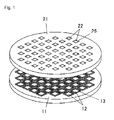
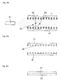
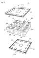
- Fig. 1 shows two wafers which are layered vertically and then are subjected to wafer level bonding.
- Each wafer has a plurality of minute devices provided thereon using a MEMS manufacturing technique or a semiconductor manufacturing technique.
- the devices to be provided on the two wafers may be a combination of any devices, for example, a combination of a MEMS device such as a sensor or a transducer and an IC device such as an IC, an LSI or an ASIC, a combination of an IC device and an IC device, or a combination of a MEMS device and a MEMS device.
- one of the two wafers may be simply a wafer for sealing having no device.
- description will be given of the combination mentioned first, that is, the case where one of the wafers has a plurality of MEMS devices provided thereon and the other wafer has a plurality of IC devices provided thereon.
- a wafer 11 (an Si wafer) has a plurality of IC devices 12 provided thereon with regular pitches, and each IC device 12 is surrounded with an insulating seal 13 (an insulating film for bonding) which is a TEOS-SiO 2 film.
- a wafer 21 (an Si wafer) has a plurality of MEMS devices 22 provided thereon with regular pitches in correspondence with the IC devices 12.
- Fig. 2 shows an exploded perspective view of a MEMS 31 obtained in such a manner that the wafer 11 and the wafer 12 are layered vertically, are integrated by bonding, and are cut by dicing.
- the MEMS device 22 is located on a substrate 21 a which is part of the wafer 21.
- the MEMS device 22 is shown as a uniaxial acceleration sensor in which a weight 32 located inside a recess 34 of the substrate 21 a is supported by a cantilever 33.
- the weight 32 is displaced vertically by sensing an acceleration, and this displacement is measured by an electrostatic capacitance method or a piezoelectric resistance method.
- measurement signals can be partly output to an electrode 23.
- the IC device 12 is located on a cover substrate 11 a which is part of the wafer 11, and processes the measurement signals from the MEMS device 22.
- the cover substrate 11 a has an inner peripheral portion surrounded with the insulating seal 13 in a frame shape.
- a plurality of electrodes 14 are formed on a periphery of a bottom surface of the cover substrate 11 a and are electrically connected to the IC device 12.
- a plurality of electrodes 23 is formed on a periphery of a top surface of the substrate 21 a.
- each of the electrodes 14 and 23 is formed in such a manner that a surface of a Cr electrode film is subjected to Au plating.
- a position of each electrode 14 corresponds to a position of each electrode 23.
- Each electrode 23 is electrically connected to a bump 25 formed on a bottom surface of the substrate 21 a through a via hole 24 which penetrates through the substrate 21 a.
- a protruding electrode 26 (an electrode for bonding) , for example made of Au, is formed on each electrode 23.
- the electrode 23 is electrically connected to the electrode 14 in such a manner that the Au protruding electrode 26 is press-fitted to the electrode 14. Therefore, the electrode 14 of the cover substrate 11 a is also electrically connected to the bump 25 formed on the bottom surface of the substrate 21 a.
- the material for the protruding electrode 26 may preferably be a metal having a hardness which is lower than that of Si, that is, 6.5 GPa, and examples thereof may include Al, Cu, Ag and the like in addition to Au.
- the insulating seal 13 formed on the cover substrate 11 a is bonded to the top surface of the substrate 21 a by a bonding method such as direct bonding or plasma bonding for activating a bonding surface as the insulating seal 13 in the wafer state shown in Fig. 1 , so that the cover substrate 11 a and the substrate 21 a are integrated.
- a bonding method such as direct bonding or plasma bonding for activating a bonding surface as the insulating seal 13 in the wafer state shown in Fig. 1 , so that the cover substrate 11 a and the substrate 21 a are integrated.
- the MEMS 31 connected to a circuit board through the bump, moreover, electric power is supplied to the IC device 12 by a route passing through any bump 25, the corresponding via hole 24, the corresponding electrode 23, the corresponding Au protruding electrode 26 and the corresponding electrode 14. Further, the measurement signals are sent from the MEMS device 22 to the IC device 12 by a route passing through any electrode 23, the corresponding Au protruding electrode 26 and the corresponding electrode 14. The signals subjected to signal processing in the IC device 12 are output to the outside by a route passing through any electrode 14, the corresponding Au protruding electrode 26, the corresponding electrode 23, the corresponding via hole 24 and the corresponding bump 25.
- Figs. 3A to 3D show schematic sectional views of steps to be carried out for forming the Au protruding electrode 26 on the wafer 21.
- Figs. 4A to 4D show schematic sectional views of steps to be carried out for forming the insulating seal 13 on the wafer 11.
- Fig. 5 shows a schematic sectional view of the state that the wafer 21 having the Au protruding electrode 26 formed thereon and the wafer 11 having the insulating seal 13 formed thereon are layered vertically and then are integrated by bonding.
- Fig. 6 shows a schematic sectional view of the MEMS 31 obtained from the vertically layered wafers 11 and 12 by dicing.
- a wafer 21 is obtained in such a manner that a plurality of MEMS devices 22 are provided on an Si wafer by use of a MEMS manufacturing technique and a plurality of via holes 24 are formed at required positions on the Si wafer.
- the wafer 21 is washed and then a TEOS-SiO 2 film is formed on a top surface of the wafer 21 by a CVD (Chemical Vapor Deposition) method, so that a substrate insulating film 27 is formed on the top surface of the wafer 21.
- CVD Chemical Vapor Deposition
- a region serving as a surface to be bonded to a wafer 11 i.e., a periphery of each MEMS device 22
- a plurality of electrodes 23 each having a two-layer structure consisting of a lower Cr layer and an upper Au layer are formed at predetermined positions on the substrate insulating film 27.
- an Au protruding electrode 26 is formed on each electrode 23.
- the wafer 11 is obtained in such a manner that a plurality of IC devices 12 are provided on an Si wafer by a semiconductor manufacturing process.
- the wafer 11 is washed and then a TEOS-SiO 2 film is formed on a top surface of the wafer 11 by a CVD method, so that a lower-layer insulating film 15 is formed on the entire top surface of the wafer 11.
- a plurality of electrodes 14 each having a two-layer structure consisting of a lower Cr layer and an upper Au layer are formed at predetermined positions on the lower-layer insulating film 15. As shown in Fig.
- a TEOS-SiO 2 film is formed on the lower-layer insulating film 15 by the CVD method in order to form an upper-layer insulating film 16. Furthermore, a TEOS-SiO 2 film is formed by the CVD method in order to form an insulating seal 13 on a region serving as a surface to be bonded to the wafer 21.
- each IC device 12 is surrounded with the insulating seal 13.
- the electrode 14 is bared from the upper-layer insulating film 16.
- the insulating seal 13 has a thickness which is considerably larger than that of the upper-layer insulating film 16.
- a total thickness H of the substrate insulating film 27, the electrode 23 and the Au protruding electrode 26 is larger than a height h of the insulating seal 13 which is measured from a surface of the electrode 14 to a top surface of the insulating seal 13.
- the IC device wafer 11 and the MEMS device wafer 21 are ready for bonding as described above, and then are washed with an organic solvent or an acid.
- the wafer 11 is turned upside down and is superimposed on the wafer 21 such that the insulating seal 13 of the wafer 11 is opposed to the bonding surface of the wafer 21 and the Au protruding electrode 26 of the wafer 21 is opposed to the electrode 14 of the wafer 11.
- the total thickness H of the substrate insulating film 27, the electrode 23 and the Au protruding electrode 26 is larger than the height h of the insulating seal 13 which is measured from the surface of the electrode 14 to the top surface of the insulating seal 13.
- the Au protruding electrode 26 is abutted against the electrode 14 of the wafer 11.
- the Au protruding electrode 26 is soft and, when the wafer 11 is pressed against the wafer 21 until the insulating seal 13 is abutted against the surface of the wafer 21, the Au protruding electrode 26 is crushed and press-fitted to the electrode 14, so that the electrode 14 is electrically connected to the electrode 23.
- the insulating seal 13 as the TEOS-SiO 2 film is bonded to the surface of the wafer 21 by direct bonding or plasma bonding such that the wafers 11 and 21 are integrated. This bonding ensures the electrical connection and, simultaneously, provides complete blockage of external atmosphere because of the complete sealing using the insulating seal 13.
- a plurality of bumps 25 are formed on a back surface of the wafer 21, and then the wafers 11 and 21, which are layered vertically, are cut with a dicing blade or the like at a position between the adjacent insulating seals 13 (along a line c-c in Fig. 5 ).
- a MEMS 31 in which the MEMS device 22 and the IC device 12 are sealed with the package formed by a substrate 21 a and a cover substrate 11 a.
- the wafers 11 and 21 are cut at the position between the adjacent insulating seals 13.
- a width of the insulating seal 13 may be made sufficiently larger than a thickness of the dicing blade such that the wafer 11 and 21 can be cut at a position where the insulating seal 13 is divided.
- the TEOS-SiO 2 film described in the manufacturing process is made of TEOS, that is, "tetraethoxysilane" Si(OC 2 H 5 ) 4 .
- SiO 2 generated from TEOS is deposited on a film formation surface, and a CVD method is employed for generating SiO 2 from TEOS.
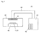
- Fig. 7 shows a plasma CVD device 41 for forming a TEOS-SiO 2 film.
- the plasma CVD device 41 includes a chamber 42 for film formation, a raw material container 43, and a supply duct 44 for coupling the chamber 42 to the raw material container 43.
- the raw material container 43 retains liquid TEOS which is supplied from a TEOS tank 45.
- the raw material container 43 is kept at a temperature of about 50°C, and vaporized TEOS in the raw material container 43 is supplied into the chamber 42 through the supply duct 44.
- the chamber 42 is kept at a low pressure of 1 to 10 Torr, and the wafer 11 or 21 is placed on a table 46.
- the wafer 11 or 21 on the table 46 is heated with a heater or the like and is kept at a substrate temperature of 200°C to 500°C (preferably, about 300°C).
- the vaporized TEOS supplied from the supply duct 44 is ejected from a shower head 47 in the chamber 42.
- the TEOS ejected from the shower head 47 is decomposed by energy of plasma discharge (i.e., bonds other than an Si-O bond are disengaged) to generate SiO 2 molecules.
- the SiO 2 molecules are deposited on the wafer 11 or 21, so that a TEOS-SiO 2 film is formed on the wafer 11 or 21.
- the wafers each having the TEOS-SiO 2 film formed thereon are bonded by the direct bonding or the like.
- This bonding method called direct bonding is implemented in accordance with a principle shown in Figs. 8A to 8C .
- the wafers 11 and 21 to be bonded are put into a chamber of a bonding device.
- the chamber is kept at a normal temperature, and a degree of vacuum (i.e., a degree of vacuum prior to activation) in the chamber is set at a high vacuum of about 1.0 ⁇ 10 -5 Pa.
- a degree of vacuum i.e., a degree of vacuum prior to activation
- the joining surfaces each having the TEOS-SiO 2 film formed thereon are subjected to the direct bonding.
- a TEOS-SiO 2 film e.g., the insulating seal 13
- Si wafer surface bared on a bonding surface of a second wafer may be subjected to the direct bonding (in a case where only one of the two bonding surfaces is activated) as in the manufacturing process shown in Fig. 5 .
- an SiO 2 film may be formed on a bonding surface of such a wafer for sealing by thermal oxidation.
- an SiO 2 film formed by sputtering may be smoothed by polishing (e.g., CMP).
- the bonding method according to one embodiment of the present invention is described. According to this method, it is possible to obtain an insulating film for bonding which has satisfactory surface smoothness and thickness evenness. That is, according to a method for forming a TEOS-SiO 2 film by a CVD method, it is possible to obtain an SiO 2 film having satisfactory surface smoothness and thickness evenness by a film forming process at a relatively low temperature.
- the relatively low temperature refers to a temperature to prevent damage to devices (e.g., IC devices) and wiring patterns provided on a wafer.
- the relatively low temperature is not more than 500°C.
- the relatively low temperature is not more than 400°C.
- Table 1 to be described below provides a result of comparison regarding surface smoothness, thickness evenness and a temperature in a film forming process among a TEOS-SiO 2 film formed by a CVD method, an SiO 2 film formed by a thermal oxidation method and an SiO 2 film formed by a sputtering method.
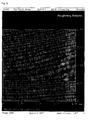
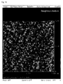
- Fig. 9 shows an enlarged microscopic photograph of the TEOS-SiO 2 film formed by the CVD method.
- Fig. 10 shows an enlarged microscopic photograph of the SiO 2 film formed by the sputtering method.
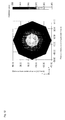
- Fig. 11 shows a variation in in-plane thickness of a TEOS-SiO 2 film formed by a CVD method on a wafer having a diameter of eight inches.
- Fig. 12 shows a variation in in-plane thickness of an SiO 2 film formed by sputtering on a wafer having a diameter of eight inches. Each wafer is normalized such that a maximum thickness is 1.000.
- the variation in in-plane thickness is not less than 5%. In Table 1, therefore, the thickness evenness in the sputtering method was evaluated as "Bad”.
- the variation in in-plane thickness is suppressed except a slight portion of an edge and the resultant thickness evenness is considerably favorable. Specifically, the variation in in-plane thickness is not more than 1%. In Table 1, therefore, the thickness evenness in the CVD method for forming the TEOS-SiO 2 film was evaluated as "Excellent" as in the thermal oxidation method.
- a substrate temperature is 200 to 500°C, preferably about 300°C. For this reason, there is no possibility that the wiring pattern and the like are damaged although this temperature is higher than that in the sputtering method.
- the process temperature in the CVD method for forming the TEOS-SiO 2 film was evaluated as "Good".
- the wafer level bonding method allows formation of an insulating film for bonding, which is excellent in surface smoothness and thickness evenness, by a low-temperature process.
- the temperature can be set at not more than 500°C, so that a step of manufacturing a MEMS 31 can be carried out as the low-temperature process by combination with direct bonding and the like.
- wiring patterns made of Al and the like and MEMS structural components are less prone to be damaged.
- use of the direct bonding and the like eliminates necessity of cooling the MEMS 31, leading to improvement of manufacturing efficiency.
- the excellent surface smoothness and thickness evenness can be attained since the TEOS-SiO 2 film formed by the CVD method is used as the insulating film for bonding. Therefore, excellent bonding strength can be attained when wafers are bonded with this insulating film for bonding being interposed therebetween in a state that insulation between the wafers is maintained. Further, use of this insulating film for bonding improves reliability at the bonded portion. Moreover, the bonding of the wafers also allows attainment of excellent sealability and hermeticity.
- the insulating film for bonding is not necessarily polished unlike an insulating film formed by a PVD method such as sputtering, and can be used as deposition, leading to improvement of a degree of freedom concerning the manufacturing process of the MEMS 31.
- the foregoing embodiment describes the case of the direct bonding shown in Figs. 8A to 8C .
- the bonding method according to this embodiment allows formation of an SiO 2 film having satisfactory smoothness and thickness evenness by a low-temperature process. Therefore, plasma bonding may be employed in place of the direct bonding.
- a weight 62 is arranged in a through hole 64 penetrating vertically through a substrate 21 a and is supported by a bidirectional cantilever 63.
- a biaxial acceleration sensor is provided as a MEMS device 22 in the substrate 21 a.
- Such a MEMS 61 has the through hole 64 which is also opened at a bottom surface thereof.
- a top surface is sealed with a cover substrate 11 a and, additionally, the bottom surface must be sealed. Therefore, the bottom surface is sealed with a cover substrate 71a.
- the cover substrate 71 a is similar in structure to the cover substrate 11a. That is, the cover substrate 71 a includes an IC device 72 and an electrode 74. Moreover, a substrate seal 73 (an insulating film for bonding) which is a TEOS-SiO 2 film is formed at a periphery of the cover substrate 71 a. On a bottom surface of the substrate 21 a, an electrode 65 and an Au protruding electrode are formed so as to be opposed to the electrode 74.
- the MEMS 61 having the three-layer structure described above is manufactured as in the MEMS having the two-layer structure. More specifically, a wafer 11 having a plurality of IC devices 12 provided thereon and a wafer 21 having a plurality of MEMS devices 22 provided thereon are subjected to direct bonding with an insulating seal 13 being interposed therebetween. Moreover, a wafer having a plurality of IC devices 72 provided thereon (i.e., a host substrate for a cover substrate 71 a) and the wafer 21 are also subjected to direct bonding with a substrate seal 73 being interposed therebetween. Thus, the MEMS 61 is obtained by dicing from the three wafers layered as described above.
- the foregoing embodiment describes the wafer level bonding (the wafer level packaging) in which substrates in a wafer state are bonded and then are cut.
- the present invention is also applicable to bonding at a chip level.
- the wafer 11 is cut to prepare a plurality of chip-like substrates 11 a
- the wafer 21 is cut to prepare a plurality of chip-like substrates 21 a.
- the chip-like substrates 11a and 21 a may be subjected to direct bonding or the like with a TEOS-SiO 2 film being interposed therebetween.
Abstract
Description
- The present invention relates to a substrate bonding method and an electronic component. More specifically, the invention relates to a substrate bonding method for layering a first substrate and a second substrate preferably comprising at least one device, preferably a MEMS device, provided thereon. More specifically, the invention relates to a substrate bonding method for layering a substrate having a device provided thereon, preferably an IC device, and a substrate having a device, preferably a MEMS device, provided thereon. In particular, the invention concerns a substrate bonding method for performing wafer level packaging on wafer substrates layered vertically as they are after assembling.
- In a step of manufacturing a MEMS (Micro Electro-Mechanical System), typically, a wafer having a plurality of MEMS devices provided thereon is diced into a plurality of chips, each chip (i.e., each MEMS device) is incorporated in a package housing, and an opening of the package housing is sealed with a cover.
- In such a manufacturing method, however, each MEMS device is subjected to packaging using a package housing and a cover, resulting in complication of the step of manufacturing the MEMS. In course of the manufacture of the MEMS, further, dust and dirt are attached to the MEMS device, resulting in reduction of yields. Moreover, restriction to the package housing hinders miniaturization of the MEMS device.
- In order to solve these problems, attention has been given to a wafer level bonding technique for packaging a MEMS device and the like in a state of a wafer, or a technique called wafer level packaging. According to this method, wafers each having a plurality of devices provided thereon, for example, a wafer having a plurality of IC devices such as CMOS provided thereon and a wafer having a plurality of MEMS devices provided thereon are layered (superimposed) vertically and then are bonded. Thus, each MEMS device and each IC device are confined in a pair within a cell formed between the wafers. Thereafter, the bonded wafers are separated into cells by dicing or the like to obtain a MEMS having a configuration that the MEMS device and the IC device are accommodated in the package formed by the wafers.
- According to this manufacturing method, since the wafers are cut with the MEMS device and the IC device being confined therebetween, dust and dirt are less prone to be attached to the MEMS device and the like. Moreover, the MEMS device having a movable part is not handled in a bare chip state, leading to enhancement of yields of MEMSs. Further, the resultant MEMS is reduced in size and the number of MEMSs to be obtained from one wafer increases, leading to reduction of manufacturing costs.
- However, there remain the following problems to be solved in order to put such a wafer level bonding technique to practical use.
- When a wafer having an IC device such as CMOS provided thereon and a wafer having a MEMS device provided thereon are layered vertically and wafer level bonding (i.e., packaging) is performed on the wafers so layered, it is necessary to achieve electrical insulation and electrical conduction simultaneously between the vertically layered wafers. For example, bonding surfaces of the wafers must be electrically insulated whereas electrodes of the respective devices must be electrically connected. For this reason, the wafers are bonded with an insulating film being interposed therebetween (e.g., refer to
JP 2007-184546 A - An SiO2 film is a typical insulating film for use in a bonding surface (e.g., refer to
JP 2007-184546 A JP 2004-160607 A JP 2007-509578 A - According to the thermal oxidation method for thermally oxidizing a surface of an Si wafer to form an insulating film (i.e., an SiO2 film), this formed SiO2 film has satisfactory surface smoothness and thickness evenness. However, the thermal oxidation method is a high-temperature process of applying heat at about 1000°C to a wafer in an oxygen atmosphere in order to form a film. Consequently, the heat causes damage on a wiring pattern formed on the wafer, resulting in breaks of the wiring pattern.
- According to the PVD method such as sputtering, on the other hand, an SiO2 film can be formed by a process at a low temperature of about 100°C. As a result, a wiring pattern on a wafer is prevented from being damaged thermally. According to the PVD method, however, the formed SiO2 film is unsatisfactory in surface smoothness and thickness evenness. Consequently, there is a problem that it is impossible to satisfactorily increase bonding strength between the SiO2 film and the wafer and to satisfactorily ensure reliability.
- In order to attain smoothness, a bonding surface is occasionally subjected to CMP (Chemical Mechanical Polishing) in manufacture of LSI and the like. However, a MEMS device has such a complicated structure that structural components, electrodes and the like are formed on both sides of a wafer. For this reason, there is a possibility that the polishing causes damage on the MEMS device. Consequently, it is impossible to attain the smoothness by the polishing, that is, it is impossible to smooth the SiO2 film formed by the PVD method, by the polishing.
- The present invention has been devised in view of the disadvantages described above, and an object thereof is to provide a substrate bonding method capable of forming a smooth SiO2 film by a process at a relatively low temperature and capable of reliably bonding substrates with the smooth SiO2 film being interposed between the substrates.
- A substrate bonding method according to the present invention comprises the steps of forming an insulating film for bonding including depositing an SiO2 film made of TEOS by a CVD method on at least one of a first substrate and a second substrate; and bonding the first substrate and the second substrate with the insulating film for bonding being interposed between the first substrate and the second substrate.
- In the substrate bonding method according to the present invention, an insulating film for bonding is formed by deposition of an SiO2 film made of TEOS. The insulating film (i.e., the TEOS-SiO2 film) formed as described above is excellent in surface smoothness and thickness evenness. Thus, the insulating film for bonding, which is formed on one of two substrates, is brought into surface contact with the other substrate, so that the substrates can be bonded firmly in a state that an insulating property between the substrates is ensured. Moreover, the insulating film for bonding is excellent in surface smoothness and thickness evenness and, therefore, requires no polishing after being formed unlike an insulating film formed by sputtering. As a result, there is no possibility that the polishing causes damage on a device, leading to facilitation of a process carried out prior to bonding of substrates and improvement of a degree of freedom concerning the process. In a method of forming an SiO2 film made of TEOS by a CVD method, moreover, the TEOS-SiO2 film can be formed at a temperature of about not more than 500°C by use of a film forming device operable at a relatively low temperature. As a result, there is no possibility that an Al wiring pattern is melted and damaged, leading to enhancement of yields of finished products and improvement of reliability.
Examples of a manner of bonding first and second substrates with an insulating film for bonding being interposed between the first and second substrates include a case where an insulating film for bonding formed on a first substrate is bonded to a surface of a second substrate, and a case where an insulating film for bonding formed on a first substrate is bonded to an insulating film for bonding formed on a second substrate. - Preferred embodiments of the method are defined by dependent claims 2-7. Preferably, the method further comprises the step of forming an electrode for bonding made of a plastically deformable metal on one of an electrode of the first substrate and an electrode of the second substrate, and the bonding step preferably comprises the step of abutting the electrode for bonding against the electrode of the substrate on which the electrode for bonding is not formed, before the insulating film for bonding is abutted against a surface of the substrate on which the insulating film for bonding is not formed, and then press-fitting to the electrode of the substrate on which the electrode for bonding is not formed. Herein, the plastically deformable metal refers to a metal which is lower in hardness than the substrate, and examples thereof include Au, Al, Cu, Ag and the like. According to this preferred embodiment, the substrates can be bonded while being electrically insulated by the insulating film for bonding and, simultaneously, the electrodes of the substrates can be bonded while being electrically connected by the electrode for bonding.
- In accordance with another preferred embodiment of the present invention, the bonding step comprises activating a bonding surface of the insulating film for bonding and bonding the first substrate and the second substrate with the insulating film for bonding being interposed therebetweenHerein, the bonding method for activating the bonding surface refers to a method for activating bonding surfaces for example by use of an ion gun or plasma and then bonding the bonding surfaces, and examples thereof include direct bonding, plasma bonding and the like. According to this preferred embodiment, the substrates can be bonded at a relatively low temperature (more preferably, a normal temperature). In this joining, therefore, there is no possibility that a wiring pattern and the like of a device are damaged. Moreover, a product is not necessarily cooled after the bonding, leading to enhancement of productivity.
- In accordance with still another preferred embodiment of the present invention, the first substrate is a wafer substrate, the second substrate is a wafer substrate comprising at least one device, preferably a plurality of devices, provided thereon, and the first substrate and the second substrate are bonded and then are cut for each region where the at least one device, preferably the plurality of devices, is(are) provided. According to this preferred embodiment, the wafer substrates are preferably bonded and then are cut for each device in order to prepare a product. Therefore, the device can be handled in a wafer state until a final stage for preparation of a product, leading to enhancement of yields of products. Herein, the bonded wafer substrates may be cut at a position between the adjacent insulating films for bonding. In such a cutting method, a load is less prone to be placed on the insulating film for bonding. Moreover, the bonded wafer substrates may be cut at a position where the insulating film for bonding is divided. According to such a cutting method, a film formation pattern of the insulating film for bonding can be facilitated.
- In accordance with yet another preferred embodiment of the present invention, the number of substrates to be bonded is not less than three. The method for bonding two substrates is preferably applied to the respective substrates, so that at least three substrates can be layered and integrated.
- According to a further aspect of the invention, an electronic component is provided. The electronic component according to the present invention includes: a first substrate; a second substrate comprising at least one device, preferably a plurality of devices, provided thereon; and an insulating film for bonding formed on at least one of the first and second substrates, the insulating film being an SiO2 film made of TEOS. The first and second substrates are bonded with the insulating film for bonding being interposed therebetween. The device is preferably sealed between the first and second substrates in such a manner that the first and second substrates are bonded with the insulating film for bonding being interposed therebetween.
- In the electronic component according to the present invention, an insulating film for bonding is formed by deposition of an SiO2 film made of TEOS. The insulating film (i.e., the TEOS-SiO2 film) formed as described above is excellent in surface smoothness and thickness evenness. Thus, the insulating film for bonding, which is formed on one of two substrates, is brought into surface contact with the other substrate, so that the substrates can be bonded firmly. Moreover, the insulating film for bonding is excellent in surface smoothness and thickness evenness and, therefore, requires no polishing after being formed unlike an insulating film formed by sputtering. As a result, there is no possibility that the polishing causes damage on a device, leading to facilitation of a process for bonding substrates. In a method of forming an SiO2 film made of TEOS, moreover, a film forming device operable at a relatively low temperature can be used. As a result, a wiring pattern and the like on a device are less prone to be damaged.
- The present invention permits to overcome the disadvantages described above, and provides a solution based on the features defined in claim 1 and preferred embodiments based on the dependent claims or other appropriate combinations of the constituent elements described above. Thus, the present invention allows numerous variations based on the combinations of the constituent elements.
-
-
Fig. 1 shows a perspective view of a manner of wafer level bonding according to one embodiment of the present invention and, more specifically, shows a manner of bonding a wafer having a MEMS device provided thereon and a wafer having an IC device provided thereon; -
Fig. 2 shows an exploded perspective view of a MEMS obtained from the bonded wafers shown inFig. 1 by dicing; -
Figs. 3A to 3D show schematic sectional views of steps to be carried out for forming an Au protruding electrode on one of the wafers; -
Figs. 4A to 4D show schematic sectional views of steps to be carried out for forming an insulating seal on the other wafer; -
Fig. 5 shows a schematic sectional view of a state that the wafer having the Au protruding electrode formed thereon and the wafer having the insulating seal formed thereon are layered vertically and then are integrated by bonding; -
Fig. 6 shows a schematic sectional view of the MEMS obtained from the vertically layered wafers by dicing; -
Fig. 7 shows a schematic view for describing a configuration of a CVD device for forming a TEOS-SiO2 film; -
Figs. 8A to 8C show schematic views for describing steps to be carried out for bonding wafers at a normal temperature; -
Fig. 9 shows a TEOS-SiO2 film observed with a microscope; -
Fig. 10 shows an SiO2 film formed by sputtering and observed with the microscope; -
Fig. 11 shows a variation in in-plane thickness of a TEOS-SiO2 film formed on a wafer; -
Fig. 12 shows a variation in in-plane thickness of an SiO2 film formed by sputtering on a wafer; and -
Fig. 13 shows an exploded perspective view of a MEMS according to another embodiment of the present invention. - With reference to the accompanying drawings, hereinafter, description will be given of preferred embodiments of the present invention.
- With reference to the drawings, first, description will be given of one embodiment of the present invention.
Fig. 1 shows two wafers which are layered vertically and then are subjected to wafer level bonding. Each wafer has a plurality of minute devices provided thereon using a MEMS manufacturing technique or a semiconductor manufacturing technique. The devices to be provided on the two wafers may be a combination of any devices, for example, a combination of a MEMS device such as a sensor or a transducer and an IC device such as an IC, an LSI or an ASIC, a combination of an IC device and an IC device, or a combination of a MEMS device and a MEMS device. Moreover, one of the two wafers may be simply a wafer for sealing having no device. In the following, description will be given of the combination mentioned first, that is, the case where one of the wafers has a plurality of MEMS devices provided thereon and the other wafer has a plurality of IC devices provided thereon. - As shown in
Fig. 1 , a wafer 11 (an Si wafer) has a plurality ofIC devices 12 provided thereon with regular pitches, and eachIC device 12 is surrounded with an insulating seal 13 (an insulating film for bonding) which is a TEOS-SiO2 film. On the other hand, a wafer 21 (an Si wafer) has a plurality ofMEMS devices 22 provided thereon with regular pitches in correspondence with theIC devices 12. -
Fig. 2 shows an exploded perspective view of aMEMS 31 obtained in such a manner that thewafer 11 and thewafer 12 are layered vertically, are integrated by bonding, and are cut by dicing. TheMEMS device 22 is located on asubstrate 21 a which is part of thewafer 21. InFig. 2 , theMEMS device 22 is shown as a uniaxial acceleration sensor in which aweight 32 located inside arecess 34 of thesubstrate 21 a is supported by acantilever 33. Theweight 32 is displaced vertically by sensing an acceleration, and this displacement is measured by an electrostatic capacitance method or a piezoelectric resistance method. Herein, measurement signals can be partly output to anelectrode 23. - The
IC device 12 is located on acover substrate 11 a which is part of thewafer 11, and processes the measurement signals from theMEMS device 22. Thecover substrate 11 a has an inner peripheral portion surrounded with the insulatingseal 13 in a frame shape. - A plurality of
electrodes 14 are formed on a periphery of a bottom surface of thecover substrate 11 a and are electrically connected to theIC device 12. On the other hand, a plurality ofelectrodes 23 is formed on a periphery of a top surface of thesubstrate 21 a. Herein, each of theelectrodes electrode 14 corresponds to a position of eachelectrode 23. Eachelectrode 23 is electrically connected to abump 25 formed on a bottom surface of thesubstrate 21 a through a viahole 24 which penetrates through thesubstrate 21 a. - Moreover, a protruding electrode 26 (an electrode for bonding) , for example made of Au, is formed on each
electrode 23. Theelectrode 23 is electrically connected to theelectrode 14 in such a manner that theAu protruding electrode 26 is press-fitted to theelectrode 14. Therefore, theelectrode 14 of thecover substrate 11 a is also electrically connected to thebump 25 formed on the bottom surface of thesubstrate 21 a. Herein, the material for the protrudingelectrode 26 may preferably be a metal having a hardness which is lower than that of Si, that is, 6.5 GPa, and examples thereof may include Al, Cu, Ag and the like in addition to Au. - Thus, the insulating
seal 13 formed on thecover substrate 11 a is bonded to the top surface of thesubstrate 21 a by a bonding method such as direct bonding or plasma bonding for activating a bonding surface as the insulatingseal 13 in the wafer state shown inFig. 1 , so that thecover substrate 11 a and thesubstrate 21 a are integrated. - In the
MEMS 31 connected to a circuit board through the bump, moreover, electric power is supplied to theIC device 12 by a route passing through anybump 25, the corresponding viahole 24, the correspondingelectrode 23, the correspondingAu protruding electrode 26 and the correspondingelectrode 14. Further, the measurement signals are sent from theMEMS device 22 to theIC device 12 by a route passing through anyelectrode 23, the correspondingAu protruding electrode 26 and the correspondingelectrode 14. The signals subjected to signal processing in theIC device 12 are output to the outside by a route passing through anyelectrode 14, the correspondingAu protruding electrode 26, the correspondingelectrode 23, the corresponding viahole 24 and thecorresponding bump 25. - With reference to
Figs. 3A to 3D throughFig. 6 , next, detailed description will be given of steps to be carried out for obtaining theMEMS 31 shown inFig. 2 from the wafer state shown inFig. 1 .Figs. 3A to 3D show schematic sectional views of steps to be carried out for forming theAu protruding electrode 26 on thewafer 21.Figs. 4A to 4D show schematic sectional views of steps to be carried out for forming the insulatingseal 13 on thewafer 11.Fig. 5 shows a schematic sectional view of the state that thewafer 21 having theAu protruding electrode 26 formed thereon and thewafer 11 having the insulatingseal 13 formed thereon are layered vertically and then are integrated by bonding.Fig. 6 shows a schematic sectional view of theMEMS 31 obtained from the vertically layeredwafers - As shown in
Fig. 3A , awafer 21 is obtained in such a manner that a plurality ofMEMS devices 22 are provided on an Si wafer by use of a MEMS manufacturing technique and a plurality of viaholes 24 are formed at required positions on the Si wafer. As shown inFig. 3B , next, thewafer 21 is washed and then a TEOS-SiO2 film is formed on a top surface of thewafer 21 by a CVD (Chemical Vapor Deposition) method, so that asubstrate insulating film 27 is formed on the top surface of thewafer 21. Herein, a region serving as a surface to be bonded to a wafer 11 (i.e., a periphery of each MEMS device 22) is masked for preventing thesubstrate insulating film 27 from being formed thereon such that the surface of thewafer 21 is bared. As shown inFig. 3C , next, a plurality ofelectrodes 23 each having a two-layer structure consisting of a lower Cr layer and an upper Au layer are formed at predetermined positions on thesubstrate insulating film 27. As shown inFig. 3D , next, anAu protruding electrode 26 is formed on eachelectrode 23. - As shown in
Fig. 4A , thewafer 11 is obtained in such a manner that a plurality ofIC devices 12 are provided on an Si wafer by a semiconductor manufacturing process. As shown inFig. 4B , next, thewafer 11 is washed and then a TEOS-SiO2 film is formed on a top surface of thewafer 11 by a CVD method, so that a lower-layer insulating film 15 is formed on the entire top surface of thewafer 11. As shown inFig. 4C , next, a plurality ofelectrodes 14 each having a two-layer structure consisting of a lower Cr layer and an upper Au layer are formed at predetermined positions on the lower-layer insulating film 15. As shown inFig. 4D , next, a TEOS-SiO2 film is formed on the lower-layer insulating film 15 by the CVD method in order to form an upper-layer insulating film 16. Furthermore, a TEOS-SiO2 film is formed by the CVD method in order to form an insulatingseal 13 on a region serving as a surface to be bonded to thewafer 21. Herein, eachIC device 12 is surrounded with the insulatingseal 13. Moreover, theelectrode 14 is bared from the upper-layer insulating film 16. The insulatingseal 13 has a thickness which is considerably larger than that of the upper-layer insulating film 16. A total thickness H of thesubstrate insulating film 27, theelectrode 23 and theAu protruding electrode 26 is larger than a height h of the insulatingseal 13 which is measured from a surface of theelectrode 14 to a top surface of the insulatingseal 13. - The
IC device wafer 11 and theMEMS device wafer 21 are ready for bonding as described above, and then are washed with an organic solvent or an acid. As shown inFig. 5 , next, thewafer 11 is turned upside down and is superimposed on thewafer 21 such that the insulatingseal 13 of thewafer 11 is opposed to the bonding surface of thewafer 21 and theAu protruding electrode 26 of thewafer 21 is opposed to theelectrode 14 of thewafer 11. Herein, the total thickness H of thesubstrate insulating film 27, theelectrode 23 and theAu protruding electrode 26 is larger than the height h of the insulatingseal 13 which is measured from the surface of theelectrode 14 to the top surface of the insulatingseal 13. Therefore, when thewafers Au protruding electrode 26 is abutted against theelectrode 14 of thewafer 11. TheAu protruding electrode 26 is soft and, when thewafer 11 is pressed against thewafer 21 until the insulatingseal 13 is abutted against the surface of thewafer 21, theAu protruding electrode 26 is crushed and press-fitted to theelectrode 14, so that theelectrode 14 is electrically connected to theelectrode 23. Next, the insulatingseal 13 as the TEOS-SiO2 film is bonded to the surface of thewafer 21 by direct bonding or plasma bonding such that thewafers seal 13. - Next, a plurality of
bumps 25 are formed on a back surface of thewafer 21, and then thewafers Fig. 5 ). As shown inFig. 6 , thus, there is obtained aMEMS 31 in which theMEMS device 22 and theIC device 12 are sealed with the package formed by asubstrate 21 a and acover substrate 11 a. InFig. 5 , thewafers seal 13 may be made sufficiently larger than a thickness of the dicing blade such that thewafer seal 13 is divided. - The TEOS-SiO2 film described in the manufacturing process is made of TEOS, that is, "tetraethoxysilane" Si(OC2H5)4. Herein, SiO2 generated from TEOS is deposited on a film formation surface, and a CVD method is employed for generating SiO2 from TEOS.
-
Fig. 7 shows aplasma CVD device 41 for forming a TEOS-SiO2 film. Theplasma CVD device 41 includes achamber 42 for film formation, araw material container 43, and asupply duct 44 for coupling thechamber 42 to theraw material container 43. Theraw material container 43 retains liquid TEOS which is supplied from aTEOS tank 45. Theraw material container 43 is kept at a temperature of about 50°C, and vaporized TEOS in theraw material container 43 is supplied into thechamber 42 through thesupply duct 44. - The
chamber 42 is kept at a low pressure of 1 to 10 Torr, and thewafer wafer - The vaporized TEOS supplied from the
supply duct 44 is ejected from ashower head 47 in thechamber 42. The TEOS ejected from theshower head 47 is decomposed by energy of plasma discharge (i.e., bonds other than an Si-O bond are disengaged) to generate SiO2 molecules. The SiO2 molecules are deposited on thewafer wafer - The foregoing film formation conditions and other film formation conditions are summarized as follows.
- Temperature in raw material chamber: about 50°C
- Pressure for film formation: 1-10 Torr
- Temperature for film formation: 200-500°C
- Plasma power: about 400 W
- Distance to susceptor: 5-20 mm
- In the manufacturing process described above, the wafers each having the TEOS-SiO2 film formed thereon are bonded by the direct bonding or the like. This bonding method called direct bonding is implemented in accordance with a principle shown in
Figs. 8A to 8C . First, thewafers Fig. 8A , when anion gun 51 emits Ar+ ions 52 toward the wafers in the chamber, the Ar+ ions 52 are sputtered to flick SiO2 molecules 53. As shown inFig. 8B , by the emission of the Ar+ ions 52 for one to 10 minute(s), the SiO2 molecules 53 are blown off andbond lines 54 are exposed in the entire bonding surface, so that the surfaces (the bonding surfaces) of thewafers Fig. 8C , the activated bonding surfaces can be bonded firmly at a normal temperature without an adhesive resin or the like being interposed therebetween. - In the description of the principle shown in
Figs. 8A to 8C , the joining surfaces each having the TEOS-SiO2 film formed thereon are subjected to the direct bonding. Alternatively, a TEOS-SiO2 film (e.g., the insulating seal 13) formed on a bonding surface of a first wafer and an Si wafer surface bared on a bonding surface of a second wafer may be subjected to the direct bonding (in a case where only one of the two bonding surfaces is activated) as in the manufacturing process shown inFig. 5 . In a case where one of the wafers is simply a wafer for sealing having no device formed thereon, an SiO2 film may be formed on a bonding surface of such a wafer for sealing by thermal oxidation. Alternatively, an SiO2 film formed by sputtering may be smoothed by polishing (e.g., CMP). - Hereinabove, the bonding method according to one embodiment of the present invention is described. According to this method, it is possible to obtain an insulating film for bonding which has satisfactory surface smoothness and thickness evenness. That is, according to a method for forming a TEOS-SiO2 film by a CVD method, it is possible to obtain an SiO2 film having satisfactory surface smoothness and thickness evenness by a film forming process at a relatively low temperature.
- Herein, the relatively low temperature refers to a temperature to prevent damage to devices (e.g., IC devices) and wiring patterns provided on a wafer. In a case of using Cu wires, for example, the relatively low temperature is not more than 500°C. In a case of using Al wires, moreover, the relatively low temperature is not more than 400°C.
- Table 1 to be described below provides a result of comparison regarding surface smoothness, thickness evenness and a temperature in a film forming process among a TEOS-SiO2 film formed by a CVD method, an SiO2 film formed by a thermal oxidation method and an SiO2 film formed by a sputtering method.
-
Table 1 CVD method (TEOS) Thermal oxidation method Sputtering method Surface smoothness Excellent Excellent Bad Thickness evenness Excellent Excellent Bad Process temperature Good Incapable Excellent -
Fig. 9 shows an enlarged microscopic photograph of the TEOS-SiO2 film formed by the CVD method.Fig. 10 shows an enlarged microscopic photograph of the SiO2 film formed by the sputtering method. - As can be observed from
Fig. 10 , in the sputtering method, surface roughness is considerably large, and an average surface roughness Ra is 3.7 nm whereas a maximum level difference Rmax is 34.3 nm. In order to bond wafers by direct bonding, desirably, the average surface roughness is not more than 1 nm whereas the maximum level difference is not more than 10 nm. For this reason, the SiO2 film formed by the sputtering method must be subjected to polishing for smoothing a surface of the SiO2 film. However, the sputtering method can not be used because the wafer can not be polished in view of presence of structural components such as an MEMS device. In Table 1, therefore, the surface smoothness in the sputtering method was evaluated as "Bad". - As can be observed from
Fig. 9 , in the CVD method for forming the TEOS-SiO2 film, surface roughness is considerably small, and an average surface roughness Ra is 0.2 nm whereas a maximum level difference Rmax is 5.7 nm. These values satisfy the requirements that the average surface roughness is not more than 1 nm and the maximum level difference is not more than 10 nm. In Table 1, therefore, the surface smoothness in the CVD method for forming the TEOS-SiO2 film was evaluated as "Excellent" as in the thermal oxidation method. -
Fig. 11 shows a variation in in-plane thickness of a TEOS-SiO2 film formed by a CVD method on a wafer having a diameter of eight inches.Fig. 12 shows a variation in in-plane thickness of an SiO2 film formed by sputtering on a wafer having a diameter of eight inches. Each wafer is normalized such that a maximum thickness is 1.000. - As shown in
Fig. 12 , according to the sputtering method, the variation in in-plane thickness is not less than 5%. In Table 1, therefore, the thickness evenness in the sputtering method was evaluated as "Bad". - As shown in
Fig. 11 , according to the CVD method for forming the TEOS-SiO2 film, the variation in in-plane thickness is suppressed except a slight portion of an edge and the resultant thickness evenness is considerably favorable. Specifically, the variation in in-plane thickness is not more than 1%. In Table 1, therefore, the thickness evenness in the CVD method for forming the TEOS-SiO2 film was evaluated as "Excellent" as in the thermal oxidation method. - In the sputtering method, moreover, a substrate temperature in a film forming process is about 100°C which is considerably low. For this reason, there is a considerably low possibility that the wiring pattern and the like are damaged. In Table 1, accordingly, the process temperature in the sputtering method was evaluated as "Excellent".
- In the thermal oxidation method, on the other hand, a substrate temperature is about 1000°C. For this reason, there is a high possibility that the wiring pattern and the like are damaged. In Table 1, accordingly, the process temperature in the thermal oxidation method was evaluated as "Incapable".
- In the CVD method for forming the TEOS-SiO2 film, a substrate temperature is 200 to 500°C, preferably about 300°C. For this reason, there is no possibility that the wiring pattern and the like are damaged although this temperature is higher than that in the sputtering method. In Table 1, accordingly, the process temperature in the CVD method for forming the TEOS-SiO2 film was evaluated as "Good".
- As described above, the wafer level bonding method according to this embodiment allows formation of an insulating film for bonding, which is excellent in surface smoothness and thickness evenness, by a low-temperature process. In the film forming process, the temperature can be set at not more than 500°C, so that a step of manufacturing a
MEMS 31 can be carried out as the low-temperature process by combination with direct bonding and the like. In this low-temperature process, wiring patterns made of Al and the like and MEMS structural components are less prone to be damaged. Moreover, use of the direct bonding and the like eliminates necessity of cooling theMEMS 31, leading to improvement of manufacturing efficiency. - The excellent surface smoothness and thickness evenness can be attained since the TEOS-SiO2 film formed by the CVD method is used as the insulating film for bonding. Therefore, excellent bonding strength can be attained when wafers are bonded with this insulating film for bonding being interposed therebetween in a state that insulation between the wafers is maintained. Further, use of this insulating film for bonding improves reliability at the bonded portion. Moreover, the bonding of the wafers also allows attainment of excellent sealability and hermeticity. In addition, the insulating film for bonding is not necessarily polished unlike an insulating film formed by a PVD method such as sputtering, and can be used as deposition, leading to improvement of a degree of freedom concerning the manufacturing process of the
MEMS 31. - The foregoing embodiment describes the case of the direct bonding shown in
Figs. 8A to 8C . The bonding method according to this embodiment allows formation of an SiO2 film having satisfactory smoothness and thickness evenness by a low-temperature process. Therefore, plasma bonding may be employed in place of the direct bonding. - The foregoing embodiment describes the case where the two wafers are bonded. Alternatively, a plurality (e.g., not less than three) of wafers may be bonded. In a
MEMS 61 shown inFig. 13 , for example, aweight 62 is arranged in a throughhole 64 penetrating vertically through asubstrate 21 a and is supported by abidirectional cantilever 63. In other words, a biaxial acceleration sensor is provided as aMEMS device 22 in thesubstrate 21 a. - Such a
MEMS 61 has the throughhole 64 which is also opened at a bottom surface thereof. In order to seal theMEMS device 22, a top surface is sealed with acover substrate 11 a and, additionally, the bottom surface must be sealed. Therefore, the bottom surface is sealed with acover substrate 71a. - The
cover substrate 71 a is similar in structure to thecover substrate 11a. That is, thecover substrate 71 a includes anIC device 72 and anelectrode 74. Moreover, a substrate seal 73 (an insulating film for bonding) which is a TEOS-SiO2 film is formed at a periphery of thecover substrate 71 a. On a bottom surface of thesubstrate 21 a, anelectrode 65 and an Au protruding electrode are formed so as to be opposed to theelectrode 74. - The
MEMS 61 having the three-layer structure described above is manufactured as in the MEMS having the two-layer structure. More specifically, awafer 11 having a plurality ofIC devices 12 provided thereon and awafer 21 having a plurality ofMEMS devices 22 provided thereon are subjected to direct bonding with an insulatingseal 13 being interposed therebetween. Moreover, a wafer having a plurality ofIC devices 72 provided thereon (i.e., a host substrate for acover substrate 71 a) and thewafer 21 are also subjected to direct bonding with asubstrate seal 73 being interposed therebetween. Thus, theMEMS 61 is obtained by dicing from the three wafers layered as described above. - The foregoing embodiment describes the wafer level bonding (the wafer level packaging) in which substrates in a wafer state are bonded and then are cut. However, the present invention is also applicable to bonding at a chip level. For example, the
wafer 11 is cut to prepare a plurality of chip-like substrates 11 a whereas thewafer 21 is cut to prepare a plurality of chip-like substrates 21 a. Thereafter, the chip-like substrates
Claims (9)
- A substrate bonding method comprising the steps of:forming an insulating film for bonding (13) including depositing an SiO2 film made of TEOS by a CVD method on at least one of a first substrate (11a) and a second substrate(21 a); andbonding the first substrate (11a) and the second substrate (21 a) with the insulating film for bonding (13) being interposed between the first substrate (11a) and the second substrate (21 a).
- The substrate bonding method according to claim 1, further comprising the step of forming an electrode for bonding (26) made of a plastically deformable metal on one of an electrode of the first substrate and an electrode (23) of the second substrate (21 a), wherein the bonding step comprises the step of abutting the electrode for bonding (26) against the electrode (14) of the substrate (11a) on which the electrode for bonding (26) is not formed, before the insulating film for bonding (13) is abutted against a surface of the substrate (11a) on which the insulating film for bonding (13) is not formed, and then press-fitting to the electrode (14) of the substrate (11a) on which the electrode for bonding (26) is not formed.
- The substrate bonding method according to claim 1, wherein the bonding step comprises activating a bonding surface of the insulating film for bonding (13) and bonding the first substrate (11a) and the second substrate (21 a) with the insulating film for bonding (13) being interposed therebetween.
- The substrate bonding method according to claim 1, wherein the first substrate (11a) is a wafer (11) substrate,the second substrate (21 a) is a wafer (21) substrate comprising at least one device (22) provided thereon, andthe first substrate (11a) and the second substrate (21 a) are bonded and then are cut for each region where the at least one device (22) is provided.
- The substrate bonding method according to claim 4, wherein
the bonded substrates (11a, 21 a) are cut at a position between the adjacent insulating film for bonding (13). - The substrate bonding method according to claim 4, wherein
the bonded substrates (11a, 21 a) are cut at a position where the insulating film for bonding (13) is divided. - The substrate bonding method according to claim 1, wherein
the number of substrates to be bonded is not less than three. - An electronic component comprising:a first substrate (11a);a second substrate (21 a) comprising at least one device (22) provided thereon; andan insulating film for bonding (13) formed on at least one of the first and second substrates (11a, 21 a), the insulating film for bonding (13) being an SiO2 film made of TEOS, whereinthe first and second substrates (11a, 21 a) are bonded with the insulating film for bonding (13) being interposed therebetween.
- The electronic component according to claim 8, wherein the at least one device (22) is sealed between the first and second substrates (11a, 21 a).
Applications Claiming Priority (1)
| Application Number | Priority Date | Filing Date | Title |
|---|---|---|---|
| JP2008182577A JP5391599B2 (en) | 2008-07-14 | 2008-07-14 | Substrate bonding method and electronic component |
Publications (3)
| Publication Number | Publication Date |
|---|---|
| EP2145855A2 true EP2145855A2 (en) | 2010-01-20 |
| EP2145855A3 EP2145855A3 (en) | 2012-08-22 |
| EP2145855B1 EP2145855B1 (en) | 2020-02-26 |
Family
ID=41133260
Family Applications (1)
| Application Number | Title | Priority Date | Filing Date |
|---|---|---|---|
| EP09165177.8A Active EP2145855B1 (en) | 2008-07-14 | 2009-07-10 | Substrate bonding method and MEMS component |
Country Status (4)
| Country | Link |
|---|---|
| US (1) | US8048772B2 (en) |
| EP (1) | EP2145855B1 (en) |
| JP (1) | JP5391599B2 (en) |
| CN (1) | CN101628705B (en) |
Families Citing this family (4)
| Publication number | Priority date | Publication date | Assignee | Title |
|---|---|---|---|---|
| CN103832970B (en) * | 2012-11-27 | 2016-06-15 | 中国科学院微电子研究所 | A kind of low-temperature wafer bonding method |
| CN104973562A (en) * | 2014-04-03 | 2015-10-14 | 中芯国际集成电路制造(上海)有限公司 | Wafer cutting method and MEMS wafer cutting method |
| CN108726470B (en) * | 2017-04-21 | 2020-02-21 | 华为技术有限公司 | MEMS chip and electrical packaging method thereof |
| WO2020149349A1 (en) * | 2019-01-16 | 2020-07-23 | 日本製鉄株式会社 | Grain-oriented electromagnetic steel sheet and method for manufacturing same |
Citations (6)
| Publication number | Priority date | Publication date | Assignee | Title |
|---|---|---|---|---|
| US5559444A (en) * | 1991-06-04 | 1996-09-24 | Micron Technology, Inc. | Method and apparatus for testing unpackaged semiconductor dice |
| EP1526567A2 (en) * | 2003-10-22 | 2005-04-27 | Sharp Kabushiki Kaisha | Bonded semiconductor device having alignment mark and fabrication method for the same |
| US20060237810A1 (en) * | 2005-04-21 | 2006-10-26 | Kirby Sand | Bonding interface for micro-device packaging |
| US20070026559A1 (en) * | 2005-07-29 | 2007-02-01 | Hewlett-Packard Development Company, L.P. | System and method for direct-bonding of substrates |
| US20070062285A1 (en) * | 2005-09-20 | 2007-03-22 | Mitsubishi Denki Kabushiki Kaisha | Electrostatic-capacitance-type acceleration sensor |
| US20070134887A1 (en) * | 2004-09-16 | 2007-06-14 | Konstantin Bourdelle | Method of manufacturing a silicon dioxide layer |
Family Cites Families (11)
| Publication number | Priority date | Publication date | Assignee | Title |
|---|---|---|---|---|
| JPH0997754A (en) * | 1995-09-29 | 1997-04-08 | Hitachi Ltd | Aligning method of single crystal laminated structure |
| JP3733933B2 (en) * | 1996-08-27 | 2006-01-11 | オムロン株式会社 | Electronic components |
| JPH10233413A (en) * | 1997-02-21 | 1998-09-02 | Nec Kansai Ltd | Semiconductor device and its manufacture and wiring board |
| JP2004160607A (en) | 2002-11-14 | 2004-06-10 | Sony Corp | Manufacturing method for micro machine |
| CN100379015C (en) | 2003-08-13 | 2008-04-02 | 胜华科技股份有限公司 | Organic luminous dual-display element |
| JP4226037B2 (en) | 2003-10-20 | 2009-02-18 | ユニバーシティ・オブ・デイトン | Ferroelectric varactor suitable for capacitive shunt switch |
| US20070023850A1 (en) * | 2005-07-30 | 2007-02-01 | Chien-Hua Chen | Bonding surfaces together via plasma treatment on both surfaces with wet treatment on only one surface |
| US7601271B2 (en) * | 2005-11-28 | 2009-10-13 | S.O.I.Tec Silicon On Insulator Technologies | Process and equipment for bonding by molecular adhesion |
| KR20070071965A (en) * | 2005-12-30 | 2007-07-04 | 삼성전자주식회사 | Silicon direct bonding method |
| US7767542B2 (en) * | 2007-04-20 | 2010-08-03 | Semiconductor Energy Laboratory Co., Ltd | Manufacturing method of SOI substrate |
| US20100015782A1 (en) * | 2008-07-18 | 2010-01-21 | Chen-Hua Yu | Wafer Dicing Methods |
-
2008
- 2008-07-14 JP JP2008182577A patent/JP5391599B2/en active Active
-
2009
- 2009-07-10 CN CN200910159812XA patent/CN101628705B/en active Active
- 2009-07-10 EP EP09165177.8A patent/EP2145855B1/en active Active
- 2009-07-14 US US12/502,735 patent/US8048772B2/en active Active
Patent Citations (6)
| Publication number | Priority date | Publication date | Assignee | Title |
|---|---|---|---|---|
| US5559444A (en) * | 1991-06-04 | 1996-09-24 | Micron Technology, Inc. | Method and apparatus for testing unpackaged semiconductor dice |
| EP1526567A2 (en) * | 2003-10-22 | 2005-04-27 | Sharp Kabushiki Kaisha | Bonded semiconductor device having alignment mark and fabrication method for the same |
| US20070134887A1 (en) * | 2004-09-16 | 2007-06-14 | Konstantin Bourdelle | Method of manufacturing a silicon dioxide layer |
| US20060237810A1 (en) * | 2005-04-21 | 2006-10-26 | Kirby Sand | Bonding interface for micro-device packaging |
| US20070026559A1 (en) * | 2005-07-29 | 2007-02-01 | Hewlett-Packard Development Company, L.P. | System and method for direct-bonding of substrates |
| US20070062285A1 (en) * | 2005-09-20 | 2007-03-22 | Mitsubishi Denki Kabushiki Kaisha | Electrostatic-capacitance-type acceleration sensor |
Non-Patent Citations (1)
| Title |
|---|
| ZHAO H. ET AL.: "Buried polysilicon hot-wire anemometer with integrated bulk micromachined channel", JOURNAL OF MICRO/NANOLITHOGRAPHY, MEMS AND MOEMS, vol. 3, no. 3, July 2004 (2004-07), pages 493-500, XP040194809, SPIE, PO Box 10 Bellingham WA 98227-0010 USA * |
Also Published As
| Publication number | Publication date |
|---|---|
| US8048772B2 (en) | 2011-11-01 |
| US20100006999A1 (en) | 2010-01-14 |
| CN101628705B (en) | 2012-10-31 |
| CN101628705A (en) | 2010-01-20 |
| EP2145855A3 (en) | 2012-08-22 |
| EP2145855B1 (en) | 2020-02-26 |
| JP5391599B2 (en) | 2014-01-15 |
| JP2010021466A (en) | 2010-01-28 |
Similar Documents
| Publication | Publication Date | Title |
|---|---|---|
| JP2024504035A (en) | Direct bonded structure | |
| CN101295691B (en) | Semiconductor packaging structure | |
| US7951649B2 (en) | Process for the collective fabrication of 3D electronic modules | |
| JP4937842B2 (en) | Semiconductor device and manufacturing method thereof | |
| US7626258B2 (en) | Cap wafer, semiconductor chip having the same, and fabrication method thereof | |
| US6822336B2 (en) | Semiconductor device | |
| US9349673B2 (en) | Substrate, method of manufacturing substrate, semiconductor device, and electronic apparatus | |
| WO2005119776A1 (en) | Semiconductor device having three-dimensional stack structure and method for manufacturing the same | |
| JP2009181981A (en) | Manufacturing process of semiconductor device, and the semiconductor device | |
| TWI594369B (en) | Cmos compatible wafer bonding layer and process | |
| JP2011527512A (en) | Semiconductor device manufacturing method and semiconductor device | |
| WO2006080337A1 (en) | Semiconductor device and method for manufacturing same, and stacked type semiconductor integrated circuit | |
| US20070013058A1 (en) | Packaging chip having interconnection electrodes directly connected to plural wafers and fabrication method therefor | |
| CN107963609A (en) | A kind of total silicon MEMS wafer-grade vacuum encapsulation methods based on anode linkage | |
| US8048772B2 (en) | Substrate bonding method and electronic component thereof | |
| US20200083190A1 (en) | Method for producing structure, and structure | |
| JP5423399B2 (en) | Manufacturing method of device with built-in capacitor and manufacturing method of package with built-in capacitor | |
| JP2002208632A (en) | Semiconductor device and method for manufacturing the same | |
| CN114188316A (en) | Packaging method and packaging structure of fan-out type stacked chip | |
| CN111799188B (en) | Thinning wafer packaging technology utilizing TSV and TGV | |
| US20060083904A1 (en) | Wiring apparatus, protecting cap for device package using the same, and a method for manufacturing them | |
| CN114171413A (en) | Packaging method and packaging structure of fan-out type stacked chip | |
| CN114455536A (en) | Wafer-level three-dimensional packaging method and structure of MEMS gas sensor | |
| CN114171406A (en) | Packaging method and packaging structure of fan-out type stacked chip | |
| CN217933781U (en) | Wiring layer structure |
Legal Events
| Date | Code | Title | Description |
|---|---|---|---|
| PUAI | Public reference made under article 153(3) epc to a published international application that has entered the european phase |
Free format text: ORIGINAL CODE: 0009012 |
|
| AK | Designated contracting states |
Kind code of ref document: A2 Designated state(s): AT BE BG CH CY CZ DE DK EE ES FI FR GB GR HR HU IE IS IT LI LT LU LV MC MK MT NL NO PL PT RO SE SI SK SM TR |
|
| AX | Request for extension of the european patent |
Extension state: AL BA RS |
|
| PUAL | Search report despatched |
Free format text: ORIGINAL CODE: 0009013 |
|
| AK | Designated contracting states |
Kind code of ref document: A3 Designated state(s): AT BE BG CH CY CZ DE DK EE ES FI FR GB GR HR HU IE IS IT LI LT LU LV MC MK MT NL NO PL PT RO SE SI SK SM TR |
|
| AX | Request for extension of the european patent |
Extension state: AL BA RS |
|
| RIC1 | Information provided on ipc code assigned before grant |
Ipc: B81C 1/00 20060101AFI20120716BHEP |
|
| 17P | Request for examination filed |
Effective date: 20121217 |
|
| STAA | Information on the status of an ep patent application or granted ep patent |
Free format text: STATUS: EXAMINATION IS IN PROGRESS |
|
| 17Q | First examination report despatched |
Effective date: 20171017 |
|
| RIC1 | Information provided on ipc code assigned before grant |
Ipc: H01L 23/00 20060101ALI20191007BHEP Ipc: H01L 21/762 20060101ALI20191007BHEP Ipc: B81C 1/00 20060101AFI20191007BHEP Ipc: H01L 23/10 20060101ALI20191007BHEP Ipc: H01L 21/50 20060101ALI20191007BHEP Ipc: H01L 21/02 20060101ALI20191007BHEP |
|
| GRAP | Despatch of communication of intention to grant a patent |
Free format text: ORIGINAL CODE: EPIDOSNIGR1 |
|
| STAA | Information on the status of an ep patent application or granted ep patent |
Free format text: STATUS: GRANT OF PATENT IS INTENDED |
|
| INTG | Intention to grant announced |
Effective date: 20191203 |
|
| GRAS | Grant fee paid |
Free format text: ORIGINAL CODE: EPIDOSNIGR3 |
|
| GRAA | (expected) grant |
Free format text: ORIGINAL CODE: 0009210 |
|
| STAA | Information on the status of an ep patent application or granted ep patent |
Free format text: STATUS: THE PATENT HAS BEEN GRANTED |
|
| AK | Designated contracting states |
Kind code of ref document: B1 Designated state(s): AT BE BG CH CY CZ DE DK EE ES FI FR GB GR HR HU IE IS IT LI LT LU LV MC MK MT NL NO PL PT RO SE SI SK SM TR |
|
| REG | Reference to a national code |
Ref country code: GB Ref legal event code: FG4D |
|
| REG | Reference to a national code |
Ref country code: CH Ref legal event code: EP |
|
| REG | Reference to a national code |
Ref country code: AT Ref legal event code: REF Ref document number: 1237416 Country of ref document: AT Kind code of ref document: T Effective date: 20200315 |
|
| REG | Reference to a national code |
Ref country code: IE Ref legal event code: FG4D |
|
| REG | Reference to a national code |
Ref country code: DE Ref legal event code: R096 Ref document number: 602009061261 Country of ref document: DE |
|
| PG25 | Lapsed in a contracting state [announced via postgrant information from national office to epo] |
Ref country code: FI Free format text: LAPSE BECAUSE OF FAILURE TO SUBMIT A TRANSLATION OF THE DESCRIPTION OR TO PAY THE FEE WITHIN THE PRESCRIBED TIME-LIMIT Effective date: 20200226 Ref country code: NO Free format text: LAPSE BECAUSE OF FAILURE TO SUBMIT A TRANSLATION OF THE DESCRIPTION OR TO PAY THE FEE WITHIN THE PRESCRIBED TIME-LIMIT Effective date: 20200526 |
|
| REG | Reference to a national code |
Ref country code: NL Ref legal event code: MP Effective date: 20200226 |
|
| REG | Reference to a national code |
Ref country code: LT Ref legal event code: MG4D |
|
| PG25 | Lapsed in a contracting state [announced via postgrant information from national office to epo] |
Ref country code: GR Free format text: LAPSE BECAUSE OF FAILURE TO SUBMIT A TRANSLATION OF THE DESCRIPTION OR TO PAY THE FEE WITHIN THE PRESCRIBED TIME-LIMIT Effective date: 20200527 Ref country code: IS Free format text: LAPSE BECAUSE OF FAILURE TO SUBMIT A TRANSLATION OF THE DESCRIPTION OR TO PAY THE FEE WITHIN THE PRESCRIBED TIME-LIMIT Effective date: 20200626 Ref country code: BG Free format text: LAPSE BECAUSE OF FAILURE TO SUBMIT A TRANSLATION OF THE DESCRIPTION OR TO PAY THE FEE WITHIN THE PRESCRIBED TIME-LIMIT Effective date: 20200526 Ref country code: LV Free format text: LAPSE BECAUSE OF FAILURE TO SUBMIT A TRANSLATION OF THE DESCRIPTION OR TO PAY THE FEE WITHIN THE PRESCRIBED TIME-LIMIT Effective date: 20200226 Ref country code: SE Free format text: LAPSE BECAUSE OF FAILURE TO SUBMIT A TRANSLATION OF THE DESCRIPTION OR TO PAY THE FEE WITHIN THE PRESCRIBED TIME-LIMIT Effective date: 20200226 Ref country code: HR Free format text: LAPSE BECAUSE OF FAILURE TO SUBMIT A TRANSLATION OF THE DESCRIPTION OR TO PAY THE FEE WITHIN THE PRESCRIBED TIME-LIMIT Effective date: 20200226 |
|
| PG25 | Lapsed in a contracting state [announced via postgrant information from national office to epo] |
Ref country code: NL Free format text: LAPSE BECAUSE OF FAILURE TO SUBMIT A TRANSLATION OF THE DESCRIPTION OR TO PAY THE FEE WITHIN THE PRESCRIBED TIME-LIMIT Effective date: 20200226 |
|
| PG25 | Lapsed in a contracting state [announced via postgrant information from national office to epo] |
Ref country code: ES Free format text: LAPSE BECAUSE OF FAILURE TO SUBMIT A TRANSLATION OF THE DESCRIPTION OR TO PAY THE FEE WITHIN THE PRESCRIBED TIME-LIMIT Effective date: 20200226 Ref country code: DK Free format text: LAPSE BECAUSE OF FAILURE TO SUBMIT A TRANSLATION OF THE DESCRIPTION OR TO PAY THE FEE WITHIN THE PRESCRIBED TIME-LIMIT Effective date: 20200226 Ref country code: SK Free format text: LAPSE BECAUSE OF FAILURE TO SUBMIT A TRANSLATION OF THE DESCRIPTION OR TO PAY THE FEE WITHIN THE PRESCRIBED TIME-LIMIT Effective date: 20200226 Ref country code: SM Free format text: LAPSE BECAUSE OF FAILURE TO SUBMIT A TRANSLATION OF THE DESCRIPTION OR TO PAY THE FEE WITHIN THE PRESCRIBED TIME-LIMIT Effective date: 20200226 Ref country code: LT Free format text: LAPSE BECAUSE OF FAILURE TO SUBMIT A TRANSLATION OF THE DESCRIPTION OR TO PAY THE FEE WITHIN THE PRESCRIBED TIME-LIMIT Effective date: 20200226 Ref country code: EE Free format text: LAPSE BECAUSE OF FAILURE TO SUBMIT A TRANSLATION OF THE DESCRIPTION OR TO PAY THE FEE WITHIN THE PRESCRIBED TIME-LIMIT Effective date: 20200226 Ref country code: PT Free format text: LAPSE BECAUSE OF FAILURE TO SUBMIT A TRANSLATION OF THE DESCRIPTION OR TO PAY THE FEE WITHIN THE PRESCRIBED TIME-LIMIT Effective date: 20200719 Ref country code: CZ Free format text: LAPSE BECAUSE OF FAILURE TO SUBMIT A TRANSLATION OF THE DESCRIPTION OR TO PAY THE FEE WITHIN THE PRESCRIBED TIME-LIMIT Effective date: 20200226 Ref country code: RO Free format text: LAPSE BECAUSE OF FAILURE TO SUBMIT A TRANSLATION OF THE DESCRIPTION OR TO PAY THE FEE WITHIN THE PRESCRIBED TIME-LIMIT Effective date: 20200226 |
|
| REG | Reference to a national code |
Ref country code: AT Ref legal event code: MK05 Ref document number: 1237416 Country of ref document: AT Kind code of ref document: T Effective date: 20200226 |
|
| REG | Reference to a national code |
Ref country code: DE Ref legal event code: R097 Ref document number: 602009061261 Country of ref document: DE |
|
| PLBE | No opposition filed within time limit |
Free format text: ORIGINAL CODE: 0009261 |
|
| STAA | Information on the status of an ep patent application or granted ep patent |
Free format text: STATUS: NO OPPOSITION FILED WITHIN TIME LIMIT |
|
| PG25 | Lapsed in a contracting state [announced via postgrant information from national office to epo] |
Ref country code: AT Free format text: LAPSE BECAUSE OF FAILURE TO SUBMIT A TRANSLATION OF THE DESCRIPTION OR TO PAY THE FEE WITHIN THE PRESCRIBED TIME-LIMIT Effective date: 20200226 Ref country code: IT Free format text: LAPSE BECAUSE OF FAILURE TO SUBMIT A TRANSLATION OF THE DESCRIPTION OR TO PAY THE FEE WITHIN THE PRESCRIBED TIME-LIMIT Effective date: 20200226 |
|
| 26N | No opposition filed |
Effective date: 20201127 |
|
| PG25 | Lapsed in a contracting state [announced via postgrant information from national office to epo] |
Ref country code: PL Free format text: LAPSE BECAUSE OF FAILURE TO SUBMIT A TRANSLATION OF THE DESCRIPTION OR TO PAY THE FEE WITHIN THE PRESCRIBED TIME-LIMIT Effective date: 20200226 Ref country code: SI Free format text: LAPSE BECAUSE OF FAILURE TO SUBMIT A TRANSLATION OF THE DESCRIPTION OR TO PAY THE FEE WITHIN THE PRESCRIBED TIME-LIMIT Effective date: 20200226 Ref country code: MC Free format text: LAPSE BECAUSE OF FAILURE TO SUBMIT A TRANSLATION OF THE DESCRIPTION OR TO PAY THE FEE WITHIN THE PRESCRIBED TIME-LIMIT Effective date: 20200226 |
|
| REG | Reference to a national code |
Ref country code: CH Ref legal event code: PL |
|
| GBPC | Gb: european patent ceased through non-payment of renewal fee |
Effective date: 20200710 |
|
| REG | Reference to a national code |
Ref country code: BE Ref legal event code: MM Effective date: 20200731 |
|
| PG25 | Lapsed in a contracting state [announced via postgrant information from national office to epo] |
Ref country code: FR Free format text: LAPSE BECAUSE OF NON-PAYMENT OF DUE FEES Effective date: 20200731 Ref country code: GB Free format text: LAPSE BECAUSE OF NON-PAYMENT OF DUE FEES Effective date: 20200710 Ref country code: LU Free format text: LAPSE BECAUSE OF NON-PAYMENT OF DUE FEES Effective date: 20200710 Ref country code: LI Free format text: LAPSE BECAUSE OF NON-PAYMENT OF DUE FEES Effective date: 20200731 Ref country code: CH Free format text: LAPSE BECAUSE OF NON-PAYMENT OF DUE FEES Effective date: 20200731 |
|
| PG25 | Lapsed in a contracting state [announced via postgrant information from national office to epo] |
Ref country code: BE Free format text: LAPSE BECAUSE OF NON-PAYMENT OF DUE FEES Effective date: 20200731 |
|
| PG25 | Lapsed in a contracting state [announced via postgrant information from national office to epo] |
Ref country code: IE Free format text: LAPSE BECAUSE OF NON-PAYMENT OF DUE FEES Effective date: 20200710 |
|
| REG | Reference to a national code |
Ref country code: DE Ref legal event code: R081 Ref document number: 602009061261 Country of ref document: DE Owner name: MMI SEMICONDUCTOR CO., LTD., JP Free format text: FORMER OWNER: OMRON CORPORATION, KYOTO, JP Ref country code: DE Ref legal event code: R081 Ref document number: 602009061261 Country of ref document: DE Owner name: MMI SEMICONDUCTOR CO., LTD., JP Free format text: FORMER OWNER: SHIGA SEMICONDUCTOR CO., LTD., YASU-SHI, SHIGA, JP |
|
| PG25 | Lapsed in a contracting state [announced via postgrant information from national office to epo] |
Ref country code: TR Free format text: LAPSE BECAUSE OF FAILURE TO SUBMIT A TRANSLATION OF THE DESCRIPTION OR TO PAY THE FEE WITHIN THE PRESCRIBED TIME-LIMIT Effective date: 20200226 Ref country code: MT Free format text: LAPSE BECAUSE OF FAILURE TO SUBMIT A TRANSLATION OF THE DESCRIPTION OR TO PAY THE FEE WITHIN THE PRESCRIBED TIME-LIMIT Effective date: 20200226 Ref country code: CY Free format text: LAPSE BECAUSE OF FAILURE TO SUBMIT A TRANSLATION OF THE DESCRIPTION OR TO PAY THE FEE WITHIN THE PRESCRIBED TIME-LIMIT Effective date: 20200226 |
|
| PG25 | Lapsed in a contracting state [announced via postgrant information from national office to epo] |
Ref country code: MK Free format text: LAPSE BECAUSE OF FAILURE TO SUBMIT A TRANSLATION OF THE DESCRIPTION OR TO PAY THE FEE WITHIN THE PRESCRIBED TIME-LIMIT Effective date: 20200226 |
|
| PGFP | Annual fee paid to national office [announced via postgrant information from national office to epo] |
Ref country code: DE Payment date: 20230531 Year of fee payment: 15 |